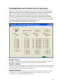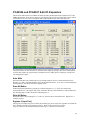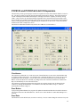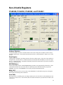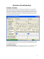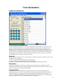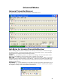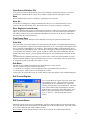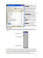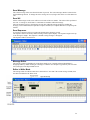
1
Win-I2CNT
I²C and SMBus Control Software
User’s Manual
Date: 01/11/2004
Information provided in this document is solely for use with Win-I2CNT. SB Solutions reserves the right to
make changes or improvements to this document at any time without notice. We assume no liability
whatsoever in the sale or use of this product, including infringement of any patent or copyright. No part of
this document may be reproduced or transmitted in any form or by any means, electronic or mechanical, for
any purpose, without the express written permission of SB Solutions.
Microsoft and Windows are registered trademarks of Microsoft Corporation.
Other brand names are trademarks or registered trademarks of their respective owners.
Questions or comments regarding this document should be emailed to support@demoboard.com.
© 1999-2004 SB Solutions. All rights reserved.
Jan 2004
2
I²C PROTOCOL................................................................................................................8
GENERAL CHARACTERISTICS .................................................................................................... 8
BIT TRANSFER ..................................................................................................................... 8
START AND STOP CONDITIONS................................................................................................ 8
I²C ADDRESS ...................................................................................................................... 8
I²C BUS DOCUMENTATION...................................................................................................... 8
DEVICES SUPPORTED IN WIN-I2CNT ............................................................................9
MAIN SCREEN.................................................................................................................9
Device Menu ............................................................................................................... 10
Message Panel ............................................................................................................ 10
Messages:................................................................................................................... 10
File Menu.................................................................................................................... 10
Save Data ................................................................................................................... 10
Load Data ................................................................................................................... 10
Options Menu.............................................................................................................. 10
I²C Frequency Menu Item ............................................................................................ 10
Calibration Menu Item.................................................................................................. 11
Parallel Port Selection Menu Item.................................................................................. 11
Mode Selection (Normal/ Slow) Menu Item .................................................................... 11
Ignore Acknowledge Menu Item ................................................................................... 11
Windows Menu............................................................................................................ 12
Help Menu .................................................................................................................. 12
Help ........................................................................................................................... 12
About ......................................................................................................................... 12
Help Hints................................................................................................................... 12
Frequency Indicator..................................................................................................... 12
Parallel Port Indicator .................................................................................................. 12
Mode Indicator ............................................................................................................ 12
System Registry Information ........................................................................................ 12
Device Driver Files ....................................................................................................... 12
CLOCK BUFFERS ...........................................................................................................13
PCK2001 / PCK2001M...................................................................................................... 13
Device Type Selection .................................................................................................. 13
Disable All Button ........................................................................................................ 13
Enable All Button ......................................................................................................... 13
Write All Button ........................................................................................................... 13
Byte 0, 1, and 2 Register.............................................................................................. 14
Automatic Write .......................................................................................................... 14
EEPROM AND RAM DEVICES ........................................................................................15
I²C Address ................................................................................................................ 15
Data Grid .................................................................................................................... 15
Set Data ..................................................................................................................... 15
Subaddress (Word Address) ......................................................................................... 16
Read Byte Button ........................................................................................................ 16
Read All Button ........................................................................................................... 16
Write Byte Button ........................................................................................................ 16
Write All Button ........................................................................................................... 16
Verify Button............................................................................................................... 16
Erase/Write Cycle Time ................................................................................................ 16
3
Page Write Size Selection ............................................................................................. 16
EEPROM Selection ....................................................................................................... 16
Goto Byte Button......................................................................................................... 16
Edit Menu ................................................................................................................... 17
I/O EXPANDERS ...........................................................................................................18
PCA9500 / PCA9501 I/O EXPANDER & EEPROM..................................................................... 18
Changing I/O Expander Data with Checkboxes............................................................... 18
Read I/O Button .......................................................................................................... 18
Set Data ..................................................................................................................... 19
Word Address ............................................................................................................. 19
Read Byte Button ........................................................................................................ 19
Read All Button ........................................................................................................... 19
Write Byte Button ........................................................................................................ 19
Write All Button ........................................................................................................... 19
PCA9554/9554A AND PCA9534 8-BIT I/O EXPANDERS ............................................................. 20
Register 0 (Input)........................................................................................................ 20
Register 1 (Output)...................................................................................................... 20
Register 2 (Polarity)..................................................................................................... 20
Register 4 (Configuration) ............................................................................................ 21
Automatic Write Enable................................................................................................ 21
Checkboxes................................................................................................................. 21
Edit Boxes................................................................................................................... 21
Read Buttons .............................................................................................................. 21
Write Button ............................................................................................................... 21
PCA9555 / PCA9535 16-BIT I/O EXPANDER ........................................................................... 22
Input Registers (subaddress 0x00 and 0x01) ................................................................. 22
Output Registers (subaddress 0x02 and 0x03) ............................................................... 22
Polarity Registers (subaddress 0x04 and 0x05)............................................................... 22
Configuration Register (subaddress 0x06 and 0x07) ....................................................... 22
Automatic Write Enable................................................................................................ 23
Checkboxes................................................................................................................. 23
Edit Boxes................................................................................................................... 23
PCA9556 AND PCA9557 8-BIT I/O EXPANDERS ........................................................................ 24
Auto Write .................................................................................................................. 24
Read All Button ........................................................................................................... 24
Write All Button ........................................................................................................... 24
Register 0 (Input Port) ................................................................................................. 24
Register 1 (Output port)............................................................................................... 25
Register 2 (Polarity)..................................................................................................... 25
Register 3 (Configuration) ............................................................................................ 25
PCF8574 AND PCF8574A 8-BIT I/O EXPANDERS ...................................................................... 26
Checkboxes................................................................................................................. 26
Read Button................................................................................................................ 26
Read Data................................................................................................................... 26
Data Byte ................................................................................................................... 27
Write Button ............................................................................................................... 27
Automatic Write Enable................................................................................................ 27
Auto Readback ............................................................................................................ 27
PCF8575 16-BIT I/O EXPANDER ........................................................................................... 28
Read Checkboxes ........................................................................................................ 28
Write Checkboxes........................................................................................................ 28
Read Button................................................................................................................ 28
Write Button ............................................................................................................... 28
Read Data Boxes ......................................................................................................... 29
Write Data Boxes......................................................................................................... 29
4
Auto Write .................................................................................................................. 29
LED BLINKERS/DIMMERS/DRIVERS ...........................................................................30
PCA9550/30 PCA9551/31 PCA9552/32 PCA9553/33....................................................... 30
Device Address............................................................................................................ 30
Auto Write On/Off Button ............................................................................................. 30
LED Mode Selector ...................................................................................................... 30
PWM Period Slide bar................................................................................................... 31
PWM Duty Cycle .......................................................................................................... 31
Write All Button ........................................................................................................... 31
Read Input Register..................................................................................................... 31
Read All Button ........................................................................................................... 31
SAA1064 LED DRIVER ....................................................................................................... 32
Control Register .......................................................................................................... 32
Automatic Write .......................................................................................................... 32
Digits 1, 2, 3, and 4 ..................................................................................................... 33
Instruction Byte........................................................................................................... 33
Read Address .............................................................................................................. 33
Status Register............................................................................................................ 33
Read Status Button...................................................................................................... 33
Write Button ............................................................................................................... 33
I2C MULTIPLEXERS.......................................................................................................34
PCA9540, PCA9542, AND PCA9544..................................................................................... 34
Control Register .......................................................................................................... 34
Interrupts ................................................................................................................... 34
Multiplexer Control ...................................................................................................... 35
Auto Write .................................................................................................................. 35
I²C SWITCHES ..............................................................................................................36
PCA9543, PCA9545, PCA9546, AND PCA9548 ...................................................................... 36
Control Register .......................................................................................................... 36
Interrupts ................................................................................................................... 36
Channel Selection ........................................................................................................ 36
Auto Write .................................................................................................................. 37
NON-VOLATILE REGISTERS .........................................................................................38
PCA8550, PCA9559, PCA9560, AND PCA9561 ...................................................................... 38
Address Selection ........................................................................................................ 38
Data Register .............................................................................................................. 38
EEPROM Byte x ........................................................................................................... 38
MUX_OUT ................................................................................................................... 38
Auto Write .................................................................................................................. 38
REAL-TIME CLOCK/CALENDARS ..................................................................................40
PCF8583 / PCF8593......................................................................................................... 40
Control/Status Register ................................................................................................ 40
Alarm Control Register ................................................................................................. 41
Write All Button ........................................................................................................... 41
Read All Button ........................................................................................................... 42
Cyclic Read ................................................................................................................. 42
Clock Registers............................................................................................................ 42
Alarm Registers ........................................................................................................... 42
Clock Controls ............................................................................................................. 43
Clock Date Controls ..................................................................................................... 43
Alarm clock controls..................................................................................................... 43
5
Alarm Date Controls..................................................................................................... 43
THERMAL MONITORS ...................................................................................................44
NE1617.......................................................................................................................... 44
Read-Only Registers .................................................................................................... 44
Write Only Registers .................................................................................................... 44
Auto Write .................................................................................................................. 44
LM75A THERMAL MONITOR .................................................................................................. 45
Device Address............................................................................................................ 45
Automatic Write (Checkbox) ......................................................................................... 45
Write All ..................................................................................................................... 45
Read All...................................................................................................................... 45
Temperature Register (Temp) ...................................................................................... 45
Thyst (Hysteresis) Register........................................................................................... 46
TOS (Overtemp shut-down threshold) Register .............................................................. 46
Configuration Register.................................................................................................. 46
Start Read Button........................................................................................................ 46
TONE GENERATORS......................................................................................................47
PCD3311/PCD3312 ......................................................................................................... 47
Tone/Frequency Selection Grid ..................................................................................... 47
Data Byte ................................................................................................................... 47
Write Button ............................................................................................................... 47
Automatic Write .......................................................................................................... 47
UNIVERSAL MODES ......................................................................................................48
UNIVERSAL TRANSMITTER/RECEIVER ....................................................................................... 48
DATA BYTES FOR UNIVERSAL TRANSMITTER/RECEIVER ................................................................. 48
Progress Bar ............................................................................................................... 49
Single Button .............................................................................................................. 49
Repeat Button ............................................................................................................. 49
Stop Button................................................................................................................. 49
Sequence Editor .......................................................................................................... 49
Delay.......................................................................................................................... 49
Send Button................................................................................................................ 49
Read/Write Bit............................................................................................................. 49
USER DEFINABLE DEVICE...................................................................................................... 50
Define New Device ...................................................................................................... 50
Open Device Definition File........................................................................................... 51
Save........................................................................................................................... 51
Save As….................................................................................................................... 51
Save Registers in text format........................................................................................ 51
Print Device Data......................................................................................................... 51
Data Grid .................................................................................................................... 51
Edit Menu ................................................................................................................... 51
Edit Current Register.................................................................................................... 51
Edit Current Device...................................................................................................... 51
Slider Control .............................................................................................................. 52
Spin Control ................................................................................................................ 53
Bit-wise Control ........................................................................................................... 53
Byte Mode .................................................................................................................. 53
EXPERT MODE ................................................................................................................... 54
Open New Page .......................................................................................................... 54
Open Data File ............................................................................................................ 54
Save Data ................................................................................................................... 54
Close Expert Mode....................................................................................................... 54
6
Add a Row .................................................................................................................. 54
Delete a Row .............................................................................................................. 54
Clear the current row................................................................................................... 55
Copy the Current Row.................................................................................................. 55
Paste Data .................................................................................................................. 55
Compress Data............................................................................................................ 55
Send Message ............................................................................................................. 56
Send All ...................................................................................................................... 56
Send Sequence ........................................................................................................... 56
Message Editor............................................................................................................ 56
Editor in Write Mode .................................................................................................... 56
Message Editor in Read Mode ....................................................................................... 57
Message Number......................................................................................................... 57
Delay after message .................................................................................................... 57
Device Address............................................................................................................ 57
Read/Write Selection ................................................................................................... 57
Send Stop ................................................................................................................... 57
Message Data ............................................................................................................. 57
Number of Bytes to Read ............................................................................................. 57
7
I²C Protocol
General Characteristics
The I²C protocol allows data to be transferred between devices using two open-drain (or open-collector) bidirectional lines. One line is the serial clock (SCL) and the other is the serial data (SDA). The bus master
generates the Start conditions, the clock signals on SCL, as well as the Stop condition. An acknowledge is
transmitted on the bus after each byte is sent over the bus.
Bit Transfer
Data on SDA must be stable while SCL is high. The state of SDA when SCL is high determines the logic
level of the transmitted data bit.
Start and STOP Conditions
Within the procedure of the I²C bus, unique situations arise which are defined as START and STOP
conditions. A HIGH to LOW transition on the SDA line while SCL is HIGH is one such unique case. This
situation indicates a START condition. A LOW to HIGH transition on the SDA line while SCL is HIGH
defines a STOP condition. The master always generates START and STOP conditions. The bus is
considered to be busy after the START condition. The bus is considered to be free again a certain time after
the STOP condition.
I²C Address
The first seven bits of an I²C transmission make up the slave address. The eighth bit (or the least significant
bit) is the R/W bit that determines the direction of the message.
A '0' in the least significant position of the first byte means that the master will WRITE information to the
selected slave. A '0' in this position means that the master will READ information from the slave.
When an I²C address is sent, each device in a system compares the first seven bits after the START
condition with its own address. If they match, the device considers itself addressed by the master as a slavereceiver or slave-transmitter, depending on the R/W bit.
When selecting addresses within Win-I2CNT, the software assumes the least significant bit is zero (write).
If the I²C message is a write transmission, the least significant bit will be sent as a ‘0’ while if it is a read,
the software will append a ‘1’ in the LSB position.
I²C Bus Documentation
The complete I²C Bus specification can be found at http://www.semiconductors.philips.com.
8
Devices supported in Win-I2CNT
Clock Buffers
PCK2001
PCK2001M
Clock / Calendar
PCF8583
PCF8593
EEPROMs
16 x 8 (128 bits)
128 x 8 (1K bits)
256 x 8 (2K bits)
512 x 8 (4K bits)
1K x 8 (8K bits)
2K x 8 (16K bits)
4K x 8 (32K bits)
8K x 8 (64K bits)
16Kx8 (128K bits)
32Kx8 (256K bits)
64Kx8 (512K bits)
I/O Expanders
PCA9534
PCA9535
PCA9554
PCA9554A
PCA9555
PCA9556
PCA9557
PCF8574
PCF8574A
PCF8575
PCA9500
PCA9501
LED Blinkers/Dimmers/Drivers
PCA9530
PCA9531
PCA9532
PCA9533
PCA9550
PCA9551
PCA9552
PCA9553
SAA1064
Master Selector
PCA9541
Multiplexers/Switches
PCA9540
PCA9542
PCA9543
PCA9544
PCA9545
PCA9546
PCA9548
Non-volatile Registers
PCA8550
PCA9559
PCA9560
PCA9561
Static RAM
PCF8570
Tone Generators
PCD3311
PCD3312
Thermal Management
LM75A
NE1617
Universal Transmitter/Receiver
From 1 to 16 registers
User Definable Device
From 1 to 256 registers
Universal Expert Mode
Main Screen
When the Win-I2CNT program starts, a screen, as shown below, will be displayed on the screen.
9
Device Menu
The device menu contains a list of I²C devices supported by the Win-I2CNT software. Selecting the device
from this menu may start any of the listed devices. You can have any combination of devices open at one
time, although only one instance of a particular device will be allowed to be active at one time. Switching
between active devices may be accomplished via the Window menu on the main toolbar.
Message Panel
The main screen has a panel that displays messages from the program. It will indicate if the I²C
transmission was successful or if there was a problem encountered. A list of messages is shown below.
Messages:
Transmission successful - the last I²C transmission was successfully completed.
Address not acknowledged - an I²C address was successfully transmitted but no slave device
acknowledged the address. A STOP condition is sent after the acknowledge clock pulse if no acknowledge
is received.
Data not acknowledged - an I²C address was previously acknowledged but one of the following data bytes
was not acknowledged. . A STOP condition is sent after the acknowledge clock pulse if no acknowledge is
received.
Read acknowledged corrupted - the master tried to send a NACK (no acknowledge) for the last read byte
in a transmission, but it was corrupted by a low level on SDA by another device on the bus.
SDA stuck low - before a START condition is initiated, the software verifies that both the SDA and SCL
lines are high. If SDA is stuck low, then an SDA stuck low message will be displayed.
SCL stuck low - before a START condition is initiated, the software verifies that both the SDA and SCL
lines are high. If SCL is stuck low, then an SCL stuck low message will be displayed.
Win-I2CNT hardware not detected- when the Win-I2CNT software is first started, it verifies that the
Win-I2CNT hardware exists at LPT1. If it is not found at LPT1, it will check LPT2, and then LPT3.
Detection is terminated when Win-I2CNT hardware is found.
The user may manually select a different port from the one selected by the program but Win-I2CNT will
again verify that hardware is available at the selected parallel port. The software will not attempt to
proceed with any transmissions until the hardware has been detected. Auto-write settings are cleared to
Auto Write Off.
File Menu
Upon starting the Win-I2C software, the file menu contains the exit and close commands. When a device
has been selected from the Device Menu, it is possible that the File Menu will also display device specific
commands such as Save As and Load. In User Device mode, previously created device files may be
conveniently loaded.
Save Data
Many devices contain the menu item 'Save Data' under the File Menu. The data may be recalled by
selecting the Load Data item under the File Menu.
Load Data
After data has been stored using the 'Save Data' item in the File Menu, it can be recalled by selecting the
Load Data item.
Options Menu
The options menu allows you to change the I²C frequency and to choose the parallel port you will use to
communicate with the I²C hardware.
I²C Frequency Menu Item
The Options Menu contains an item labeled ‘I²C Frequency’. By choosing this menu item, you will
activate a dialog box, which shows the current I²C frequency and the maximum I²C clock speed
available on the current parallel port. The speed/type of processor, as well as the chipset, used in your
computer and the mode (‘slow’ or ‘normal’) determine the maximum frequency.
Pressing the OK button will close the dialog box and will update the I²C frequency panel on the main
screen. The frequency information will be stored in the Registry and will be recalled when the
program starts again at a later time.
10
You can expect data rates over 100 kHz with a Pentium class computer, however, many factors
influence the maximum data rate and your results may vary significantly. Many I²C devices are not
designed to operate at frequencies above 100 kHz and may cause communication errors if operated
beyond 100 kHz. Lower I²C frequencies may be needed for long cable runs or excessive bus
capacitance situations. We have tested the software using the Win-I2CNT hardware at the end of
printer cables, as long as 25 feet, with no problems at frequencies over 100 kHz, however, your results
may vary.
Although the accuracy of the I²C clock frequency measurement is typically better than ±5%, it is up to
the user to verify the actual clock frequency. The frequency shown assumes no clock stretching or
long rise times. The I²C clock frequency cannot be guaranteed.
Calibration Menu Item
When Win-I2CNT is first started, it will attempt to calibrate the parallel port. Recalibration is also
performed when a new parallel port is selected as well as changing between the 'slow' and 'normal'
modes. This calibration is generally accurate to within ±5%, however, if the frequency is not as
accurate as desired, try selecting the 'Calibrate' item in the Options menu.
Parallel Port Selection Menu Item
The Options menu contains a list of three potential parallel port selections: LPT1, LPT2, and LPT3.
The parallel port's address is listed beside the port name (for example: LPT1: 0378h). Only available
ports will be listed as selectable. Parallel ports, which are not available, will be dimmed (gray).
Therefore, if you only have one parallel port in your computer, you will not have the ability to switch
to a different parallel port.
When the program starts, it scans the available ports for the I²C hardware. The user is notified if it
cannot be found, otherwise, the when it is found, the selected parallel port will have a check mark
placed beside it in the Options menu. When a new parallel port is selected from the Options menu, the
change takes effect immediately.
The selected port will also be displayed in the Parallel Port Indicator in the lower right corner of the
screen.
Mode Selection (Normal/ Slow) Menu Item
The Mode Selection defines the present state of the parallel port kernel-mode driver. ‘Normal’ access
provides higher performance access to the parallel port, but may fail if the port is already in use by
another kernel-mode driver. While slower, ‘Slow’ access provides more reliable access to ports that
have already been opened by another kernel-mode driver. If the driver fails while in ‘Normal’ access
mode, a ‘Privileged Instruction’ error may be encountered. In this situation, it is recommended to keep
the driver in ‘Slow’ mode on that computer.
The mode may be changed either by choosing the Normal Access item in the Options menu or by
clicking on the Mode Indicator.
Ignore Acknowledge Menu Item
Normally, the software checks the acknowledge bit, after every byte written, to ensure that the slavereceiver has pulled the SDA line low. When the Ignore Acknowledge item is checked in the Options
menu, the software ignores the acknowledge bit state during writes, so it is important to note that the
user will not have any feedback whether or not a device is actually receiving the message.
11
Windows Menu
The Windows Menu contains screen commands such as cascade, tile, arrange all icons, and minimize all.
If there are devices active in the program, you will find them listed in this menu. When multiple device
types are open, it is easy to move between the device types by clicking on the desired item in this menu.
Help Menu
Help
Help may be activated at any time in the program by choosing Help from the Help Menu. Pressing the
F1 key may also activate context-sensitive help.
About
Selecting the About menu item will activate the About Box. This box gives information such as
program revision level and date. It also displays the email address for contacting The Boardshop for
technical assistance with this product.
Help Hints
The main screen contains a panel at the bottom that gives a short description of the item the cursor is
currently above. By moving the cursor around the screen with the mouse, you will find that almost all
buttons, boxes, and other controls have these hints.
Frequency Indicator
The frequency at which the program is sending I²C messages over the parallel port is shown in this box on
the main screen. You can change the frequency by activating the I²C Frequency item in the Options menu.
Although the typical accuracy of the clock frequency measurement is better than +/-5%, it is up to the user
to verify the actual clock frequency. The displayed I²C clock frequency cannot be guaranteed.
Parallel Port Indicator
The main screen has an area in the bottom right hand part of the screen that shows the active parallel port.
This port can be changed by selecting a different port from the Options menu. This box is empty if no
hardware has been found.
Mode Indicator
The Mode Indicator shows the present state of the parallel port kernel-mode driver. ‘Fast’ access provides
higher performance access to the parallel port, but may fail if the port is already in use by another kernelmode driver. While slower, ‘Slow’ access provides more reliable access to ports that have already been
opened by another kernel-mode driver. If the driver fails while in ‘Fast’ access mode, a ‘Privileged
Instruction’ error may be encountered and it is recommended to keep the driver in ‘Slow’ mode on that
computer.
The mode can be switched by clicking on the Mode Indicator or by clicking on the appropriate item in the
Options menu.
System Registry Information
During the installation, important data is added to the system registry for Windows NT/2000/XP
installations in order for the port driver to function correctly. If this data is not properly installed, the driver
will not start and you will not be able to send data to the parallel port.
If the data was not found, it is very likely that there was a problem during the installation of the WinI2CNT software. If the driver is not functioning correctly, due to invalid/incorrect registry information or
missing device driver files, you will not be allowed to access the Options menu.
Device Driver Files
When the program begins, it checks to make sure that the device driver is working properly. If it is not, it
will check for the presence of the driver in the appropriate directory. If the driver is not started, you will not
be allowed to access the Options menu. The following files are required for proper operation of the WinI2CNT program:
Windows 95, Windows 98, and Windows ME: files Tvichw32.vxd and TVicHW32.dll must be located in
the Windows/System folder. No special entries are required in the System Registry for Windows
95/98/ME.
Windows NT and Windows 2000: file Tvichw32.sys must be located in the WinNT/System32/Drivers
folder.
12
Clock Buffers
PCK2001 / PCK2001M
The PCK2001 is a 1–18 fan-out buffer used for 133/100 MHz CPU, 66/33 MHz PCI, 14.318 MHz REF, or
133/100/66 MHz SDRAM clock distribution. Eighteen outputs are typically used to support up to 4
SDRAM DIMMS commonly found in desktop, workstation or server applications.
All clock outputs meet Intel's drive, rise/fall time, accuracy, and skew requirements. An I²C interface is
included to allow each output to be enabled/disabled individually. An output disabled via the I²C interface
will be held in the LOW state. In addition, there is an OE input which 3-States all outputs.
Device Type Selection
A drop down selection box allows the user to choose one of two available clock buffers:
The PCK2001 1:18 clock buffer
The PCK2001M 1:10 clock buffer
Disable All Button
All buffer outputs are put into a disabled state (shown as dark green boxes). Note that the actual data will
only be sent via the I²C bus if ‘Auto Write’ has been enabled. If ‘Auto Write’ is not enabled, then the user
should push the ‘Write All’ button to send the data to the PCK2001(M).
Enable All Button
All buffer outputs are put into an enabled state (shown as light green boxes). Note that the actual data will
only be sent via the I²C bus if ‘Auto Write’ has been enabled. If ‘Auto Write’ is not enabled, then the user
should push the ‘Write All’ button to send the data to the PCK2001(M).
Write All Button
The current state of Byte 0, Byte 1, and Byte 2 registers, shown on-screen, will be sent to the PCK2001(M)
when the Write All button is pressed.
13
Byte 0, 1, and 2 Register
Clicking on the LEDs will change the state of the output. An enabled output is shown light green while a
disabled output is shown dark green. The contents of the registers are shown in hexadecimal above the
checkboxes.
Automatic Write
If ‘Auto Write On’ is enabled (light green), any changes to the PCK2001(M) data bytes will immediately
be sent via the I²C bus. ‘Auto Write Off’ is shown in red when it is disabled.
14
EEPROM and RAM Devices
Upon starting any memory device, such as an EEPROM or RAM, you will see a screen similar to the one
shown below.
I²C Address
A drop-down menu is provided which allows the user to select a valid address for the selected device type.
Data Grid
The data grid consists of rows and columns. Each cell within the grid contains a two digit hexadecimal
number. Each cell corresponds to a physical byte location within the memory device. For example, in the
diagram below, cell 0x13 is highlighted (row 1, column 3).
This translates to address 19 (decimal) in the device. The program calculates the physical address for you
and displays it at the left side of the screen in the box labeled ‘Word Address’ or ‘Subaddress’.
Set Data
All the cells of the memory grid will be filled with the two digit hexadecimal number found in the Preset
edit box when the Set Data button is pressed. No information will be sent over the I²C bus.
15
Subaddress (Word Address)
The subaddress (sometimes called word address) is a pointer to a register or memory location within the
I²C device. To access this location, the software will send out the device I²C address, followed by this
subaddress, followed by the read or write data. The program displays the subaddress of the active cell of
the memory grid in both hexadecimal and decimal notation.
Read Byte Button
Pressing the 'Read Byte' button initiates a read from the I²C device. The program begins the transmission
by writing the word address, found in the Word Address or Subaddress box, to the device. The word
address of the currently selected cell is shown in the Word Address box on the screen. A Repeated Start is
then generated, followed by a read of the single byte. The result of each byte read is immediately entered
in the appropriate cell in the grid. In addition to pressing the 'Read Byte' button, you may press the <Alt>
and <b> keys simultaneously to achieve the same results.
Read All Button
Pressing the 'Read All' button initiates a read from the I²C device. The program begins the transmission by
writing the word address 0 to the device. A Repeated Start is then generated, followed by sequential reads
of the entire device. In addition to pressing the 'Read All' button, you may press the <Alt> and <r> keys
simultaneously to achieve the same results.
Write Byte Button
Pressing the 'Write Byte' button initiates a Write to the I²C device. The program begins the transmission by
writing the slave address and then the word address of the currently active cell in the grid. The selected
data byte is then sent. In addition to pressing the 'Write Byte' button, you may press the <Alt> and <y>
keys simultaneously and achieve the same results.
Write All Button
Pressing the 'Write All' button initiates a Write to the I²C device. The program begins the transmission by
writing the word address 0 to the device and sequentially writes the entire device.
For a RAM type device, the data is sent in one long message. In the case of an EEPROM, the software will
send one page of data (usually 8 bytes but check the datasheet for the particular device you are addressing)
followed by a STOP condition. Following the STOP condition, the program waits a length of time,
determined by the Erase/Write cycle time of the device (again check the datasheet for the device you are
programming), before writing another page to the device. In addition to pressing the 'Write All' button, you
may press the <Alt> and <w> keys simultaneously to achieve the same results.
After the completion of the write cycle, Win-I2CNT will read the entire device to verify that the contents of
the device match the data that was sent. An error message will be displayed if the data is not verified.
Verify Button
The verify button will cause Win-I2CNT to begin reading the contents of the EEPROM. After completion
of the read cycle, it will compare the contents of the EEPROM with the contents of the data grid. A
message will be displayed, if an error is found, showing the address of the failed location.
Erase/Write Cycle Time
Programming software must allow a certain period of time to elapse after writing a block of data to an
EEPROM. This time is device dependent but is normally between 10ms and 40ms. A STOP condition
must be performed before the erase/write cycle commences. Most EEPROMs will not respond to their
address until the erase/write cycle has been completed.
Page Write Size Selection
The Page Write Size defines the number of bytes which may be written in a single erase/write cycle.
Smaller devices generally use an 8 or 16 byte page while larger devices use up to 64 bytes per page. Check
the device datasheet to find the supported page size. If you do not know the page size, use a small page
size such as 8 bytes. A smaller page size will require a longer total programming time for a device.
EEPROM Selection
For the larger EEPROM sizes (>32K bits), you can choose between five EEPROM sizes from a drop-down
list. Only one type can be active within Win-I2CNT at a time.
Goto Byte Button
The Goto Byte button contains a plus sign (+) which allows the user to change the function of the button.
16
Pressing the plus (+) will show cause the button to expand as shown below:
Changing the function of the button does not cause that function to be performed. After a change, the user
must press the button to complete the function.
Goto Byte brings up a dialog box which allows
the user to input an address to jump to.
Fill Grid with… brings up a dialog box that
allows the user to fill a block of the EEPROM with a
byte of data
Copy Block will copy one block of data in the
grid from one address to another
Fill with Checkerboard fills alternating
rows with 0x55 and 0xAA
Fill with Inverse Checkerboard fills the
grid with alternating rows of 0xAA and 0x55
Edit Menu
The edit menu contains the same functions as the Goto Button described above.
17
I/O Expanders
PCA9500 / PCA9501 I/O Expander & EEPROM
The PCA9500 and PCA9501 (note that these devices were previously released as the PTN3500 and
PTN3501) provides general-purpose remote I/O expansion for most microcontroller families via the I²C
bus. The device consists of an 8-bit quasi bi-directional port and an I²C interface. The PCA950x has low
current consumption and includes latched outputs with high current drive capability for directly driving
LEDs.
The I/O expander and the EEPROM in these devices respond to different addresses. For example, the
PCA9500’s I/O expander will respond to addresses in the 0x40 to 0x4F range while the EEPROM responds
to addresses 0xA0 to 0xAF range.
Changing I/O Expander Data with Checkboxes
The ports, labeled P7 – P0 can be set high or low by clicking on them with a mouse. A high logic level is
indicated with a light green color while a low logic level is shown as a dark green color. If a port state is
changed, the data byte box in the write area will be updated to reflect the changes. The new data can be
sent to the PCA950x by pressing the Write Button. If the Auto Write On is enabled (light green), any
change in the state of the Write checkboxes or Write Data Byte will immediately be sent to the PCA950x.
Read I/O Button
Upon pressing the Read Button, the program will update the hexadecimal data shown beside the Write I/O
button as well as show the state of the individual I/Os. The I/O port is low if the port is shown in dark
green and is high if it is light green.
18
Set Data
All the cells of the memory grid will be filled with the two digit hexadecimal number found in the Preset
edit box when the Set Data button is pressed. No information will be sent over the I²C bus.
Word Address
The Word Address (also called subaddress) is a pointer to a register or memory location within the I²C
device. To access this location, the software will send out the device I²C address, followed by this
subaddress, followed by the read or write data. The program displays the subaddress of the active cell of
the memory grid in both hexadecimal and decimal notation.
Read Byte Button
Pressing the 'Read Byte' button initiates a read from the I²C device. The program begins the transmission
by writing the word address, found in the Word Address or Subaddress box, to the device. The word
address of the currently selected cell is shown in the Word Address box on the screen. A Repeated Start is
then generated, followed by a read of the single byte. The result of each byte read is immediately entered
in the appropriate cell in the grid. In addition to pressing the 'Read Byte' button, you may press the <Alt>
and <b> keys simultaneously to achieve the same results.
Read All Button
Pressing the 'Read All' button initiates a read from the I²C device. The program begins the transmission by
writing the word address 0 to the device. A Repeated Start is then generated, followed by sequential reads
of the entire device. In addition to pressing the 'Read All' button, you may press the <Alt> and <r> keys
simultaneously to achieve the same results.
Write Byte Button
Pressing the 'Write Byte' button initiates a Write to the I²C device. The program begins the transmission by
writing the slave address and then the word address of the currently active cell in the grid. The selected
data byte is then sent. In addition to pressing the 'Write Byte' button, you may press the <Alt> and <y>
keys simultaneously and achieve the same results.
Write All Button
Pressing the 'Write All' button initiates a Write to the I²C device. The program begins the transmission by
writing the word address 0 to the device and sequentially writes the entire device.
The software will send one page of data (4 bytes) followed by a STOP condition. In addition to pressing
the 'Write All' button, you may press the <Alt> and <w> keys simultaneously to achieve the same results.
After the completion of the write cycle, Win-I2CNT will read the entire device to verify that the contents of
the device match the data that was sent. An error message will be displayed if the data is not verified.
19
PCA9554/9554A and PCA9534 8-bit I/O Expanders
The PCA9554 and PCA9554A are 16-pin CMOS devices that provide 8 bits of General Purpose parallel
Input/Output (GPIO) expansion for I2C/SMBus applications and were developed to enhance the Philips
family of I2C I/O expanders. The improvements include higher drive capability, 5V I/O tolerance, lower
supply current, individual I/O configuration, 400 kHz clock frequency, and smaller packaging.
The PCA9554/54A consist of an 8-bit Configuration register (Input or Output selection); 8-bit Input
register, 8-bit Output register and an 8-bit Polarity inversion register. The system master can enable the
I/Os as either inputs or outputs by writing to the I/O configuration bits. The data for each Input or Output is
kept in the corresponding Input or Output register. The polarity of the read register can be inverted with the
Polarity Inversion Register. All registers can be read by the system master.
The PCA9554 and PCA9554A differ only in their slave addresses.
Register 0 (Input)
This register is a read only port. It reflects the incoming logic levels of the pins, regardless of whether the
pin is defined as an input or an output by Register 3. Writes to this register have no effect.
Register 1 (Output)
This register reflects the outgoing logic levels of the pins defined as outputs by Register 3. Bit values in this
register have no effect on pins defined as inputs. Reads from this register return the value that is in the flipflop controlling the output selection, NOT the actual pin value.
Register 2 (Polarity)
This register allows the user to invert the polarity of the Input Port Register data. If a bit in this register is
set (written with ‘1’), the corresponding Input Port data is inverted. If a bit in this register is cleared
(written with a ‘0’), the Input Port data polarity is retained.
20
Register 4 (Configuration)
This register configures the directions of the I/O pins. If a bit in this register is set, the corresponding port
pin is enabled as an input with high impedance output driver. If a bit in this register is cleared, the
corresponding port pin is enabled as an output. At reset, the I/Os are configured as inputs with a weak pullup to VDD.
Automatic Write Enable
When Auto Write is enabled (light green), any changes made to Registers 1, 2, or 3 checkboxes will cause
the program to write the new data to the PCA9554(A). The display will read 'Auto Write Off' in when it is
disabled and 'Auto Write On' in when enabled.
Checkboxes
The checkboxes indicate the logic level of the various bits in the registers. A checked box is equivalent to
logic ‘1’ while an unchecked box is equivalent to logic ‘0’. The logic level can be changed by single
clicking on the checkbox. If Auto Write is enabled (checked), Win-I2CNT will write the new value to the
PCA9554.
Edit Boxes
The edit boxes show the current hexadecimal value for each of the 4 registers. Register 0 is a Read-Only
register so the user cannot change this value. If the hexadecimal value is changed by the user, it will be
transmitted by Win-I2CNT if the Auto Write is on (checked).
The checkboxes will also be updated to reflect the new value of the Edit Box.
Read Buttons
Upon pressing one of the Read Buttons, Win-I2CNT will read the appropriate register and place the
hexadecimal value in the edit box. The checkboxes are updated to reflect the individual bit logic levels.
Pressing the Read All button reads all four registers.
Because the PCA9554 and PCA9554A do not automatically increment the register address between
operations, only one register may be read for each Start condition sent. Therefore, after Register 0 has been
read by Win-I2CNT, a Restart will be sent so that Register 1 can be read. This will continue until all four
registers have been read and then a Stop condition will be transmitted.
Write Button
Upon pressing one of the Write Buttons, Win-I2CNT will write to the appropriate register. Pressing the
Write All button writes to Registers 1, 2, and 3.
Since there is no automatic increment of the register subaddress between writes, only one register may be
written for each Start condition. Therefore, after Register 1 has been written by Win-I2CNT, a Restart will
be sent out so that Register 2 can be written. Register 3 is then written followed by a Stop condition.
21
PCA9555 / PCA9535 16-bit I/O Expander
The PCA9555 is a 24-pin CMOS device that provide 16 bits of General Purpose parallel Input/Output
(GPIO) expansion for I2C/SMBus applications and was developed to enhance the Philips family of I2C I/O
expanders. The improvements include higher drive capability, 5V I/O tolerance, lower supply current,
individual I/O configuration, and smaller packaging. I/O expanders provide a simple solution when
additional I/O is needed for ACPI power switches, sensors, pushbuttons, LEDs, fans, etc.
The PCA9555 consist of two 8-bit Configuration (Input or Output selection); Input, Output and Polarity
inversion (Active high or Active low operation) registers. The system master can enable the I/Os as either
inputs or outputs by writing to the I/O configuration bits. The data for each Input or Output is kept in the
corresponding Input or Output register. The polarity of the read register can be inverted with the Polarity
Inversion Register. All registers can be read by the system master.
Input Registers (subaddress 0x00 and 0x01)
These registers are read-only. They reflect the incoming logic levels of the pins, regardless of whether the
pin is defined as an input or an output by the Configuration Registers. Writes to this register have no effect.
Output Registers (subaddress 0x02 and 0x03)
These registers reflect the outgoing logic levels of the pins defined as outputs by the Configuration
Registers. Bit values in this register have no effect on pins defined as inputs. Reads from this register return
the value that is in the flip-flop controlling the output selection, NOT the actual pin value.
Polarity Registers (subaddress 0x04 and 0x05)
These registers allow the user to invert the polarity of the Input Port Register data. If a bit in this register is
set (written with ‘1’), the corresponding Input Port data is inverted. If a bit in this register is cleared
(written with a ‘0’), the Input Port data polarity is retained.
Configuration Register (subaddress 0x06 and 0x07)
The Configuration Registers define the directions of the I/O pins. If a bit in these register is set, the
corresponding port pin is enabled as an input with high impedance output driver. If a bit in these registers is
22
cleared, the corresponding port pin is enabled as an output. At reset, the I/Os are configured as inputs with
a weak pull-up to VDD.
Automatic Write Enable
When Auto Write On is enabled (green), any changes made to Registers 1 through 7 checkboxes will cause
the program to write the new data to the PCA9555. The display will read 'Auto Write Off' when it is
disabled and 'Auto Write On' when enabled.
Checkboxes
The checkboxes indicate the logic level of the various bits in the registers. A checked box is equivalent to
logic ‘1’ while an unchecked box is equivalent to logic ‘0’. The logic level can be changed by single
clicking on the checkbox. If Auto Write is enabled (green LED), Win-I2CNT will write the new value to
the PCA9555 immediately after a change is made.
Edit Boxes
The edit boxes show the current hexadecimal value for each of the 4 registers. Register 0 is a Read-Only
register so the user cannot change this value. If the hexadecimal value is changed by the user, it will be
transmitted by Win-I2CNT if the Auto Write is on (checked). The checkboxes will also be updated to
reflect the new value of the Edit Box.
Read Buttons
Upon pressing one of the Read Buttons, Win-I2CNT will
read the appropriate register and place the hexadecimal
value in the edit box. The checkboxes are updated to reflect
the individual bit logic levels.
In the top left corner of the button, there is a plus (+) sign.
Clicking on the (+) brings up a menu above button. The
menu allows the user to change the function of the button so
that either the low or high register can be read or both can
be read.
Write Button
Upon pressing one of the Write Buttons, Win-I2CNT will
write to the appropriate register. The function of the
button can be changed by pressing on the (+) symbol in the
top left corner of the button. When pressed, a menu will
pop up allowing the user to write the lower, upper, or both
registers.
23
PCA9556 and PCA9557 8-bit I/O Expanders
The PCA9556 and PCA9557 are CMOS circuit that provides parallel input/output expansion for I2C and
SMBus applications. These devices consist of an 8-bit input port register, 8-bit output port register, and an
I2C interface. It has low current consumption and a high impedance open drain output pin, I/O0.
T
he system master can reset the PCA9556 in the event of a timeout by asserting a LOW on the reset input.
The system master can also invert the PCA9556/PCA9557 inputs by writing to their active HIGH polarity
inversion bits. Finally, the system master can enable the I/Os as either inputs or outputs by writing to the
I/O configuration register.
Auto Write
When the Auto Write On is enabled (green), any changes made by the user to the PCA9556/PCA9557
Registers 1, 2, and 3 will immediately be sent to the PCA9556/PCA9557. If an error is encountered during
this transmission, Auto Write Off will be displayed (red).
Read All Button
Each time the Read All button is pressed, the contents of Registers 0, 1, 2, and 3 are read from the
PCA9556/PCA9557. The register data will be reflected in the state of the checkboxes, with an unchecked
box indicating logic '0' and a checked box indicating logic '1'.
Write All Button
When this button is pressed, Registers 1, 2, and 3 are written to the PCA9556/PCA9557. Register 0 is a
read-only register.
Register 0 (Input Port)
This register is an input-only port. It reflects the incoming logic levels of the pins, regardless of whether the
pin is defined as an input or an output by register 3. Writes to this register have no effect.
Logic '0' is shown as an unchecked checkbox while logic '1' is shown as a checked box.
24
Register 1 (Output port)
This register is an output-only port. It reflects the outgoing logic levels of the pins defined as outputs by
register 3. Bit values in this register have no effect on pins defined as inputs. In turn, reads from this
register reflect the value that is in the flip-flop controlling the output selection, NOT the actual pin value.
Register 2 (Polarity)
This register enables polarity inversion of pins defined as inputs by register 3. If a bit in this register is set
(written with ‘1’), the corresponding port pin’s polarity is inverted. If a bit in this register is cleared (written
with a ‘0’), the corresponding port pin’s original polarity is retained.
Register 3 (Configuration)
This register is an input-only port. It reflects the incoming logic levels of the pins, regardless of whether the
pin is defined as an input or an output by register 3. Writes to this register have no effect. This register
configures the directions of the I/O pins. If a bit in this register is set (written with ‘1’), the corresponding
port pin is enabled as an input with high impedance output driver. If a bit in this register is cleared (written
with ‘0’), the corresponding port pin is enabled as an output.
25
PCF8574 and PCF8574A 8-bit I/O Expanders
The PCF8574 provides general-purpose remote I/O expansion for most microcontroller families via the I²C
bus. The device consists of an 8-bit quasi bi-directional port and an I²C interface. The PCF8574 has low
current consumption and includes latched outputs with high current drive capability for directly driving
LEDs. It also possesses an open-drain interrupt output that can be connected to the interrupt logic of the
microcontroller. By sending an interrupt signal on this line, the remote I/O can inform the microcontroller
if there is incoming data on its ports without having to communicate via the I²C bus. This means that the
PCF8574 can remain a simple slave device.
The PCF8574 and PCF8574A differ only in their slave addresses (as shown below).
Checkboxes
The checkboxes, labeled P0 - P7, in the write areas of the PCF8574(A) screen can be checked/unchecked
by clicking on them with a mouse. If a checkbox state is changed, the data byte box in the write area will
be updated to reflect the changes. The new data can be sent to the PCF8574(A) by pressing the Write
Button. If the Auto Write On is checked, any change in the state of the Write checkboxes or Write Data
Byte will immediately be sent to the PCF8574(A).
The checkboxes found in the Read PCF8574(A) panels are read only and can only be changed by the
software by clicking the Read buttons. If a checkbox is checked, this indicates a logic '1', while an
unchecked box indicates a logic '0'.
Read Button
Upon pressing the Read Button, the program will update the hexadecimal data shown beside the button as
well as show the state of the individual I/Os. The I/O is low if the checkbox is unchecked and high if it is
checked.
Read Data
The Read boxes on the PCF8574(A) screens are read-only. The user cannot change the contents of any edit
26
boxes or checkboxes in this area. The information is updated only by pressing the Read Button.
Data read from the PCF8574(A) will be shown in the box beside the Read Button. The checkboxes are
then changed to show the value of each individual I/O of the device. If the checkbox is checked, then the
I/O pin is high while an unchecked box means that the I/O pin is low.
It is important to remember that before any I/Os in the PCF8574(A) can be used as inputs, they must be set
high first. The program does not do this for you.
Data Byte
Any two digit hexadecimal number may be entered in this data box. When it is changed, the checkboxes
labeled P0 - P7 will also change showing the current value of the data which will be written to the
PCF8574(A).
Write Button
Pressing the Write Button will send an I²C message to the PCF8574(A) consisting of: a Start condition, the
I²C address, the data byte, followed by the Stop condition. Note that if Automatic Write Enable is checked,
any changes to the data box will be sent any time a change is made.
Automatic Write Enable
When Auto Write On is enabled (light green), any changes made to the P0-P7 checkboxes will cause the
program to write the new data to the PCF8574(A). The display will read 'Auto Write Off' when it is
disabled and 'Auto Write On' when enabled.
Auto Readback
When this function is enabled (light green), the software will immediately read the PCF8574 after it has
performed a write. The result of the read will be displayed in the Read groupbox.
27
PCF8575 16-bit I/O Expander
The PCF8575 is a CMOS circuit which provides general purpose remote I/O expansion for most microcontroller
families via the two-line bi-directional bus (I²C-bus).
The device consists of a 16-bit quasi bi-directional port and an I²C-bus interface. The PCF8575 has a low current
consumption and includes latched outputs with high current drive capability for directly driving LEDs. It also possesses
an interrupt line (INT) which can be connected to the interrupt logic of a microcontroller. By sending an interrupt
signal on this line, the remote I/O can inform the microcontroller if there is incoming data on its ports without having to
communicate via the I²C bus. This means that the PCF8575 is an I²C-bus slave transmitter/receiver.
Every data transmission from the PCF8575 must consist of an even number of bytes; the first byte will be referred to as
P07 to P00 and the second byte as P17 to P10. The third will be referred to as P07 to P00 and so on.
Read Checkboxes
There are sixteen checkboxes in the Read box. The contents of the PCF8575 are read by pressing the Read
button. A checked item indicates logic '1' while an unchecked item means logic '0'. The user cannot change
the checkboxes since these are read-only.
Write Checkboxes
Clicking on the checkboxes will invert the current state of the bit. Logic '0' is shown as an unchecked box
while logic '1' is shown as a checked box. If Auto Write is on, then any changes made to these checkboxes
will immediately be sent to the PCF8575.
Read Button
When this button is pressed, the two eight bit registers are read via the I²C bus.
Data from Port 0 is read first, followed by Port 1. The data bytes are displayed in the area beside the Read
button and the checkboxes are updated.
Write Button
When the Write button is pressed, the contents of the High and Low data boxes are sent to the PCF8575 via
the I²C bus.
28
Read Data Boxes
These two boxes show the port state of the PCF8575 in hexadecimal format.
These boxes cannot be directly modified by the user but must be changed by pressing the read button.
Write Data Boxes
The user can change the contents of the register by entering a two digit hexadecimal number into the upper
and/or lower edit boxes. If the Auto Write is enabled, both data registers are sent, even if only one is
changed.
Auto Write
When the Auto Write is enabled (light green), any changes made by the user to the PCF8575 checkboxes
on the screen will immediately be sent to the PCF8575 via the I²C bus.
29
LED Blinkers/Dimmers/Drivers
PCA9550/30 PCA9551/31 PCA9552/32 PCA9553/33
The PCA955x LED Blinker blinks LEDs in I2C applications where it is necessary to limit bus traffic or free
up the I2C Master’s (MCU, MPU, DSP, chipset, etc.) timer. The uniqueness of this device is the internal
oscillator with two programmable blink rates. To blink LEDs using normal I/O Expanders like the
PCF8574 or PCA9554, the bus master must send repeated commands to turn the LED on and off. This
greatly increases the amount of traffic on the I2C bus and uses up one of the master’s timers. The PCA955x
LED Blinker instead requires only the initial set up command to program BLINK RATE 1 and BLINK
RATE 2 (i.e., the frequency and duty cycle) for each individual output.
Device Address
The device I2C address can be selected by choosing one of the hexadecimal selections from the drop down
list. The default address at start-up is 0xC0.
Auto Write On/Off Button
When Auto Write is disabled (LED off), the software can be modified without transmitting data to through
the parallel port. When the Auto Write LED is on, any changes made to the software is immediately
transmitted to the PCA955x.
LED Mode Selector
Each LED can be set in one of four modes: ON, OFF, PWM0, and PWM1. The mode is selected by
moving the switches to the appropriate mode for the LED. All LEDs set to PWMx will blink at the same
frequency, duty cycle, and phase.
30
PWM Period Slide bar
The period of the PCA955x can be changed by moving the PWM0 or PWM1 slide bars. The period (in
seconds) and frequency (in Hertz) is displayed below the slide bar. The actual value of the PCA955x
register is displayed in the Registers groupbox.
PWM Duty Cycle
The duty cycle for PWM0 and PWM1 can be changed by moving the PWM0 or PWM1 slide bars. The
duty cycle is displayed (in percent) below the slide bar. The actual value of the PCA955x register is
displayed in the Registers groupbox.
Write All Button
Pressing the Write All button causes Registers 1 through 6 to be programmed.
Read Input Register
When the Read Input register button is pressed, the Input register is read and the data is presented in the
Registers groupbox.
Read All Button
Pressing the Read All button will read all the device registers from the PCA955x using the auto-increment
feature. Since the PCA955x devices don’t allow auto-increment starting from Register 0, the reads start
with the register with the highest address which causes the auto-increment pointer to roll-over to Register 0
(Input Register). The reads continue until the all the registers have been read.
The data will be displayed in the Registers groupbox and the controls (sliders, switches) will be updated.
31
SAA1064 LED Driver
When the SAA1064 is chosen from the device menu, the following screen will appear on your monitor.
Control Register
The Control Register is responsible for determining the mode of operation of the SAA1064. It can control
which digits are blanked, static versus dynamic operation, and the current supplied to the LEDs.
In order to change the value of the Control Register in the SAA1064, the state of the checkboxes in the
Control Register box on the screen can be toggled (checked/unchecked) and the slider can be used to
change the current sinking of the device.
The figure below shows the contents of the Control Register.
C6 = 1
C5 = 1
C4 = 1
C3 = 1
C2 = 0/1
C1 = 0/1
C0 = 0
C0 = 1
adds 12mA to segment output current
adds 6mA to segment output current
adds 3mA to segment output current
all segment outputs are switched on for segment test
digits 2 and 4 are blanked/not blanked
digits 1 and 3 are blanked/not blanked
static mode (continuous display of digits 1 and 2)
dynamic mode (alternating display of digit 1 + 3 and 2 + 4)
Automatic Write
If the Automatic Write is enabled (green), any changes to the SAA1064 Control Register or Digits will
32
immediately be sent via the I²C bus.
The data sent to the SAA1064 consists of a Start condition, the I²C address, Instruction byte, then the data
for the changed Control Register or Data byte, followed by the Stop condition. Therefore, a total of three
bytes will be sent any time a change is made and Automatic Write is enabled.
Digits 1, 2, 3, and 4
The SAA1064 can drive up to four 8-segment LEDs. The data for these digits is contained in four registers
within the SAA1064. In order to change the contents of these registers, you can click on the LEDs within
the Digit groupboxes. If an LED is on (light green), then the LED segment is on while a dark green LED
causes the LED segment to turn off. Changes in the on-screen LEDs are reflected in the hexadecimal
values shown above the on-screen LEDs.
If the Automatic Write is enabled (light green), any changes to the SAA1064 Control Register or LED
Digits will immediately be sent to the device through I²C bus.
Instruction Byte
The instruction byte is equivalent to a subaddress. The instruction byte is configured as shown below:
The bits SC, SB and SA of the instruction byte form a pointer and determine to which register the data byte
following the instruction byte will be written. All other bytes will then be stored in the registers with
consecutive subaddresses. This feature is called Auto-Increment (AI) of the subaddress and enables a quick
initialization by the master. The subaddress pointer will wrap around from 7 to 0.
The Win-I2CNT software does not allow the user to modify the instruction byte. The software points to 00h
when the write button is pressed since it will be writing all the registers. When Automatic Write is enabled,
the instruction byte will point to the register that is affected by the changes. For example, if the user clicks
on Bit 5 in Digit 4, then the software will set the instruction byte to 04h for the write sequence.
Read Address
This box reflects the I²C address that is sent to the SAA1064 when a read operation is performed. The
contents of this box cannot be changed directly by the user, but can only be changed by clicking on a
different address in the Device Address box.
Status Register
Only one bit is present in the status byte: the Power Reset flag. If the most significant bit is a logic ‘1’, this indicates
the occurrence of a power failure since the last time it was read out. After completion of the READ action, this flag
will be set to logic ‘0’. The LED beside the read button will illuminate if the Power Reset flag is set.
Read Status Button
When the Read Button is pressed, the contents of the Status Register is read from the SAA1064. The LED
beside the read button will illuminate if the Power Reset flag is set.
Write Button
When the Write Button is pressed, seven bytes are sent over the I²C bus, equivalent to the Address,
Instruction byte, Control byte, and then the four Digit bytes.
33
I2C Multiplexers
PCA9540, PCA9542, and PCA9544
The PCA954x is a family of bi-directional translating multiplexers, controlled via the I²C bus. The
SCL/SDA upstream pair fans out to SCx/SDx downstream pairs, or channels. Only one SCx/SDx channel
is selected at a time, determined by the contents of the programmable control register. Interrupt inputs (not
available in the PCA9540), one for each of the SCx/SDx downstream pair, are provided. One interrupt
output, which acts as an AND of the four interrupt inputs, is provided. All I/O pins are 5 V tolerant.
The pass gates of the multiplexer are constructed such that the Vdd pin can be used to limit the maximum
high voltage that will be passed by the PCA954x. This allows the use of different bus voltages on each
SCx/SDx pair, so that 3.3V parts can communicate with 5V parts without any additional protection.
External pull-up resistors can pull the bus up to the desired voltage level for this channel.
Control Register
This register selects the active multiplexer channel as well as indicating any interrupting inputs.
The control register edit box is read-only. The contents of the control register can be changed by selecting
a new channel in the Channel Select box or reading the status with the Read Button.
Interrupts
The PCA9544 and PCA9542 provide interrupt inputs; one for each channel and one open drain interrupt
output. When an interrupt is generated by any device, it will be detected by the PCA954x and the interrupt
output will be driven LOW. The channel need not be active for detection of the interrupt. A bit is also set in
the control byte. Bits 4 – 7 of the control byte correspond to channels 0 – 3 of the PCA9544, respectively,
while bits 4 and 5 are used by the PCA9542. Therefore, if an interrupt is generated by any device connected
34
to channel 2, then bit 6 will be set in the control register. Likewise, an interrupt on any device connected to
channel 3 would cause bit 7 of the control register to be set. The master can then address the PCA954x and
read the contents of the control byte to determine which channel contains the device generating the
interrupt.
The master can then reconfigure the PCA954x to select this channel, and locate the device generating the
interrupt and clear it. The interrupt clears when the device originating the interrupt clears.
It should be noted that more than one device could be providing an interrupt on a channel, so it is up to the
master to ensure that all devices on a channel are interrogated for an interrupt.
Multiplexer Control
The user can change the selected channel by clicking the appropriate radio button. At start-up, no channel
is selected.
Auto Write
When the Auto Write On is enabled (illuminated), any changes made by the user to the PCA954x channel
selection radio buttons will immediately be sent to the device via the I²C bus.
35
I²C Switches
PCA9543, PCA9545, PCA9546, and PCA9548
The PCA9543/9545/9546/9548 are a family of bi-directional translating switches, controlled via the I²C
bus. The SCL/SDA upstream pair fans out to SCx/SDx downstream pairs, or channels. Multiple SCx/SDx
channels may be selected at a time, determined by the contents of the programmable control register.
Interrupt inputs, one for each of the SCx/SDx downstream pair, are provided. One interrupt output, which
acts as an AND of the four interrupt inputs, is provided. The interrupt inputs can also be used as general
purpose inputs. All I/O pins are 5V tolerant.
The pass gates of the switches are constructed such that the Vdd pin can be used to limit the maximum high
voltage that will be passed by the PCA954x.
Control Register
This register selects the active switch channel(s) as well as indicating any interrupting inputs.
Selecting a new channel in the Channel Select box or reading the status with the Read Button can change
the contents of the control register.
Interrupts
When an interrupt is generated by a downstream device, it will be detected by the PCA954x and the
interrupt output will be driven LOW. The channel need not be active for detection of the interrupt.
Interrupts are indicated with an illuminated LED on the screen. The interrupt bits are read-only.
Channel Selection
The user can change the selected channel(s) by clicking the appropriate checkboxes in the Channel Select
box.
36
Auto Write
When the Auto Write On is enabled (checked), any changes made by the user to the PCA954x channel
selection radio buttons will immediately be sent to the device via the I²C bus. If not checked, the write
button will need to be pressed before the data is sent to the PCA954x.
37
Non-Volatile Registers
PCA8550, PCA9559, PCA9560, and PCA9561
Address Selection
A drop down address selection is available which can be used to change the I²C address of the PCA9559,
PCA9560, and PCA9561. Note that the PCA8550 does not have a programmable I²C address as it is fixed
at 0x9C.
Data Register
Clicking on the checkboxes will change the state of the non-volatile register. If the state of the checkbox is
changed while ‘Automatic Write’ is enabled (checked), then the data will immediately be sent to the target
device. If ‘Automatic Write’ is disabled (unchecked), then the Write button must be pressed to send the I²C
message to the target device.
EEPROM Byte x
The PCA9560 and PCA9561 contain EEPROM data bytes that can be programmed by Win-I2CNT. Enter
a hexadecimal number into each of the edit boxes and then press the Write EEx button to program the
EEPROM. The value of the EEPROM can be read by pressing the Read EEx button.
MUX_OUT
The MUX_OUT pins can be set to the values in the EEPROM or from the MUX_IN pins by selecting the
desired state from the drop-down combo box.
Auto Write
When Auto Write is enabled (green), any changes made by the user to the devices will immediately be sent
to the device via the I²C bus. If not checked, the write button will need to be pressed before the data is sent
to the device.
38
39
Real-time Clock/Calendars
PCF8583 / PCF8593
The PCF8583 and PCF8593 are CMOS clock/calendar circuits, optimized for low power consumption.
Addresses and data are transferred serially via the two-line bi-directional I²C bus. The built-in word
address register is incremented automatically after each written or read data byte. The built-in 32.768 kHz
oscillator circuit and the first 8 bytes of RAM are used for the clock/calendar and counter functions. The
next 8 bytes may be programmed as alarm registers (note that Win-I2CNT will not allow you to use the
alarm registers as general purpose RAM - therefore you cannot change this data directly but must use the
on-screen alarm controls to make the changes).
Note: only the clock/calendar function of the PCF8583 are supported. The additional RAM above address
0x15 is not directly addressable by this screen. You can always use the User Definable Device Screen if
you need the RAM contents as well.
Control/Status Register
The control/status register is defined as memory location 0x00 with free access for reading and writing via
the I²C bus. All functions and options are controlled by the contents of the control/status register.
40
Alarm Control Register
When the alarm enable bit of the control/status register is set (address 0x00, bit 2), the alarm control
register (address 0x08) is activated. All alarm, timer, and interrupt output functions are controlled by the
contents of the alarm control register.
Write All Button
The write all button sends the contents of the sixteen registers to the devices via the I²C bus.
41
Read All Button
The read all button sends the appropriate commands via the I²C bus to read the contents of the sixteen
registers within the PCF8583/8593. The on-screen controls will be updated with the register data.
When the PCF8583 and PCF8593 are first started, the register data is random so it is recommended that the
registers be initialized with valid data before a read is performed.
Cyclic Read
Win-I2CNT will read registers 0x00 through 0x15 constantly when this button is pressed. The button will
indicate it is reading by showing 'On'. It will not be possible to close the program while the software is in a
cyclic read mode. Pressing the button a second time will stop Win-I2CNT from performing further reads
and the button will show 'Off'.
Clock Registers
In the clock modes 24 hour or 12 hour format can be selected by setting the most significant bit of the hours
counter register. The year and date are packed into memory location 0x05. The weekdays and months are
packed into memory location 0x06. When reading these memory locations the year and weekdays are
masked out when the mask flag of the control/status register is set. This allows the user to read the date
and month count directly. In the event counter mode, events are stored in BCD format. D5 is the most
significant and D0 the least significant digit. The divider is bypassed.
Alarm Registers
An alarm signal is generated when the contents of the alarm registers match the contents of the involved
counter registers bit-by-bit. The year and weekday bits are ignored in a dated alarm. A daily alarm ignores
the month and date bits. When a weekday alarm is selected, the contents of the alarm weekday/month
register will select the weekdays on which an alarm is activated.
In the 12 hour mode, bits 6 and 7 of the alarm hours register must be the same as the hours counter.
Note: the alarm registers cannot be changed directly by the user (with the exception of 0x07 and 0x0F).
They can only be updated by changing the appropriate controls on the PCF8583/8593 screen.
42
Clock Controls
The various spin controls, within in the Clock Time panel, can be used to change the clock time. Changes
made here will be reflected in the Clock Registers edit boxes shown near the top of the screen. The
AM/PM radio buttons determine the state of the AM/PM flag within the hours counter (register 0x04). The
12 Hour checkbox determines the format of the time. If it is checked (logic '1'), the clock is in 12-hour
format and the AM/PM flag will be updated by the PCF8583/8593. If it is unchecked (logic '0'), then the
AM/PM flag remains unchanged.
Clock Date Controls
The three controls within the 'Clock Date' box determine the register values of the PCF8583/8593. When
Win-I2CNT first displays the PCF8583/8593, it shows the current date. The user can modify the date by
changing the controls within this box. Note that the clock/calendar devices don't actually show a year.
Years are defined as 0 through 3, with year 0 being a leap year. Win-I2CNT takes the current year and
substitutes the appropriate integer (0 to 3) in the clock registers.
Alarm clock controls
Use the various spin controls to change the alarm time. Changes made here will be reflected in the Alarm
Registers edit boxes shown near the top of the screen. The AM/PM radio buttons determine the state of the
AM/PM flag within the hours counter (register 0x0C). The 12 Hour checkbox determine the format of the
time. If it is checked (logic '1'), the clock is in 12 hour format and the AM/PM flag will be updated by the
PCF8583/8593. If it is unchecked (logic '0'), then the AM/PM flag remains unchanged.
Alarm Date Controls
The three controls within the 'Alarm Date' box determine the register values of the PCF8583/8593. When
Win-I2CNT first displays the PCF8583/8593, it shows the current date. The user can modify the date by
changing the controls within this box. Note that the clock/calendar devices don't actually define a specific
year. Years are defined as 0 through 3, with year 0 being a leap year. Win-I2CNT takes the current year
and substitutes the appropriate integer (0 to 3) in the clock registers.
If weekday alarms are chosen, the calendar is substituted with checkboxes beside the days of the week. A
checkbox indicates that the alarm is set for that day while it is not set if the checkbox is unchecked.
43
Thermal Monitors
NE1617
The figure below shows the screen of the NE1617.
Read-Only Registers
The following data registers can be read by Win-I2CNT:
0x00 RIT Read Internal Temperature
0x01 RET Read External Temperature
0x02 Status Byte
0x03 RC Read Configuration
0x04 RCR Read Conversion Rate
0x05 RIHL Read Internal High Limit Temperature
0x06 RILL Read Internal Low Limit Temperature
0x07 REHL Read External High Limit Temperature
0x08 RELL Read External Low Limit Temperature
Write Only Registers
The following data registers can be written to by Win-I2CNT:
0x09 WC Write Configuration Register
0x0A WCR Write Conversion Rate Register
0x0B WIHL Write Internal High Limit Temperature
0x0C WILL Write Internal Low Level Temperature
0x0D WEHL Write External High Level Temperature
0x0E WELL Write External Low Limit Temperature
Auto Write
The Write-Only registers can automatically be sent to the NE1617 upon changing the on-screen state when
this function is enabled.
44
LM75A Thermal Monitor
The LM75A is a temperature-to-digital converter using an on-chip band-gap temperature sensor and
Sigma-delta A-to-D conversion technique. The device is also a thermal detector providing an over-temp
detection output. The LM75A contains a number of data registers: Configuration register (Conf) to store
the device settings such as device operation mode, OS operation mode, OS polarity and OS fault queue;
temperature register (Temp) to store the digital temp reading, and set-point registers (Tos & Thyst) to store
programmable over-temperature shutdown and hysteresis limits, that can be communicated by a controller
via the 2-wire serial I2C-bus interface. The device also includes an open-drain output (OS) which becomes
active when the temperature exceeds the programmed limits. There are three selectable logic address pins
allowing eight devices can be connected on the same bus without address conflict.
Device Address
A drop-down menu is provided which allows the user to select a valid address for the selected device type.
Automatic Write (Checkbox)
When this item is enabled (indicator shown in green), any changes to the Thyst, TOS, or Configuration
Register will immediately be sent to the LM75A.
Write All
Pressing this button will send data to the Thyst, TOS, and Configuration Registers.
Read All
Pressing this button will read all the registers in the LM75A.
Temperature Register (Temp)
The Temp register holds the digital result of temperature measurement or monitor at the end each A-to-D
conversion. This register is read only and contains two 8-bit data bytes consisting of one most significant
45
(MS) data byte and one least significant (LS) data byte. However, only 11 bits of those two bytes are used
to store the Temp data in 2’s complement format with the resolution of 0.125°C
Notice that when the Temp register is read, all 16 bits are provided to the bus and must all be collected by
the controller to complete the bus transaction. However, only the 11 most significant bits should be used,
and the 5 LSB bits of the LS byte are zero and should be ignored.
Thyst (Hysteresis) Register
The Thyst register defines the hysteresis for the device Watchdog operation. At the end of each conversion
the Temp data will be compared with the data stored in this register.
The Thyst register contains two 8-bit data bytes consisting of one MS data byte and one LS data byte the
same as the Temp register. However, only 9 bits of the Thyst register are used to store the set-point data in
2’s complement format with the resolution of 0.5°C.
The Thyst Register data may be changed by pressing the up/down arrows and then pressing the Write
button. The data can also be sent automatically by pressing the up/down arrow while the Auto Write
checkbox is checked.
TOS (Overtemp shut-down threshold) Register
The TOS register is used to store the user-defined overtemp shut-down threshold (Tos) for the device
Watchdog operation. At the end of each temperature conversion the Temp data will be compared with the
data stored in this register in order to set the state of the device OS output.
The TOS register contains two 8-bit data bytes consisting of one MS data byte and one LS data byte the
same as the Temp register. However, only 9 bits of the two bytes are used to store the set-point data in 2’s
complement format with the resolution of 0.5 °C.
The TOS Register data may be changed by pressing the up/down arrows and then pressing the Write
button. The data can also be sent automatically by pressing the up/down arrow while the Auto Write
checkbox is checked.
Configuration Register
The Configuration register is a write/read register and contains an 8-bit non-complement data byte that is
used to configure the device for different operation conditions. The Configuration register table shows the
bit assignments of this register.
Bit
Name
R/W POR
Description
B7–B5 Reserved
R/W
000
Reserved for the manufacturers use.
B4–B3 OS Fault Queue
R/W
00
For OS Fault Queue programming.
Programmable queue data = 0, 1 , 2, 3 for queue value =
1, 2, 4, 6 respectively. Default = 0.
B2
OS Polarity
R/W
0
For OS Polarity selection.
1 = OS active HIGH, 0 = OS active LOW (default).
B1
OS Comp/Interrupt R/W
0
For OS operation Mode selection.
1 = OS interrupt, 0 = OS comparator (default).
B0
Shut-down
R/W
0
For Device Operation Mode selection.
1 = Shut-down, 0 = Normal (default).
Start Read Button
The temperature data can be continuously read by pressing the Start Read button. The time elapsed
between each successive read transmission can be programmed by changing the value in the box above the
Start Read button. The temperature history is displayed in the graph above the button.
46
Tone Generators
PCD3311/PCD3312
Tone/Frequency Selection Grid
The Tone/Frequency grid contains a list of tones and frequencies which the PCD3311 and PCD3312 can
generate. Listed beside the tones, you will find the hexadecimal code that will be sent to the device to
generate that tone. Upon clicking on the desired tone in the grid, you will see that the data byte in the
Address/Data box also changes to reflect the new data. You can move up and down in the grid by clicking
with your mouse or by using the up/down arrows on your keyboard. If Automatic Write is enabled, any
changes made to the tone/frequency will immediately be written to the device via the I²C bus; otherwise,
the Write Button must be pressed to send the I²C message.
Data Byte
This box reflects the data that will be sent to the PCD3311/PCD3312 when the write button is pressed. The
information can be changed by:
1. Enter a two digit hexadecimal number between 00h and 3Fh
2. Click on the desired tone/frequency in the Tone/Frequency grid.
The data can be sent by pressing the Write Button or by enabling the Automatic Write feature.
Write Button
Pressing the Write Button will send an I²C message to the PCD3311/PCD3312 consisting of a Start
condition, device address, data byte, and Stop condition. Simultaneously pressing the <Alt> and <w> keys
achieves the same result as pressing the Write Button.
Automatic Write
If ‘Auto Write On’ is enabled (LED on), any changes to the PCD3311 or PCD3312 data byte will
immediately be sent via the I²C bus. Auto Write Off is shown on the button and the LED is off when it is
disabled. The data byte is changed by either selecting a different tone/frequency from the grid or by
entering a two digit hexadecimal number, between 0x00 and 0x3F in the data byte box. Automatic Write
will be switched off if an error is encountered during an I²C transmission.
47
Universal Modes
Universal Transmitter/Receiver
The figure below shows the screen of the Universal I²C Transmitter/Receiver.
Data Bytes for Universal Transmitter/Receiver
Each I²C Message (dataset) contains a maximum of 16 data bytes. The data bytes are shown as two digit
hexadecimal numbers. Only valid hexadecimal numbers can be entered into each box. Non-hexadecimal
keyboard entries will be ignored with the following exceptions:
INSERT key - pressing this key adds an extra edit box to the Message. The maximum number of data
bytes is 16, so the INSERT key will be ignored if there are already 16 bytes present.
DELETE key - pressing this key deletes the data byte where the cursor presently is shown. The software
requires that you keep at least one data byte in the Message. It will also not let you delete the address byte
or R/W bit following a restart. If you want to delete a restart, make sure the cursor is in the Start box and
then press the DELETE key.
S (Restart) key - a restart condition may be inserted into any Message location by pressing the S key on
your keyboard. The software deletes the boxes after the repeated start condition and then inserts 'S00WFF'.
An example of a message with a restart condition is shown below.
48
R (Read) key - is a read condition. This may be changed to a write condition by pressing the ‘w’ key.
W (Write) key - is a write condition. This may be changed to a read condition by pressing the ‘r’ key
Progress Bar
The progress bar is visible when the Repeat sequence button is pressed and is invisible when the
transmission has stopped. It is used as a visual cue that there is a transmission underway.
Single Button
Pressing the Single Button starts the transmission of I²C messages shown in the Sequence editor box. After
the last message in the Sequence Editor box has been transmitted, the I²C transmissions are terminated. A
delay is inserted between each I²C message if the Delay box is greater than zero.
The transmission is terminated with a Stop condition as soon as an error is encountered.
Repeat Button
Pressing the Repeat Button starts the transmission of messages shown in the Sequence editor box. After
the last I²C message in the Sequence Editor box is transmitted, the I²C transmissions are started once again
with the first message shown in the Sequence Editor box. A delay is inserted between each message if the
Delay box is greater than zero.
The transmission is terminated as soon as an error is encountered.
Stop Button
Pressing the Stop button will terminate a Repeat Sequence. However, Win-I2CNT will complete the entire
sequence before the I²C transmission ends.
Sequence Editor
The user changes the sequence editor to reflect the order in which the I²C messages will be sent via the I²C
bus. The sequence editor allows from 1 to 10 digits to be entered. Only digits 1, 2, 3, 4 and 5 are allowed
in the box since there are only 5 messages. For example, if you entered 35123441 into the sequence editor
box, message 3 will be sent, followed by message 5, followed by message 1, etc.
Delay
A delay can be inserted between messages by increasing the value of the number in the Delay box. The
number is measured in milliseconds.
Send Button
Pressing the Send Button will send the currently active message. Clicking in any edit box, in the desired
message, will change the active message. The active message is shown above the send button.
Read/Write Bit
The Read/Write bit determines whether the I²C message will read or write to a device via the I²C bus. If
this box is an R, then the address byte will end with a logic ‘1’. If this box is a ‘W’, then the address byte
will end with a logic ‘0’. An ‘R’ (read) will be changed to write by pressing the ‘w’ key, while a ‘W’ will
be changed to ‘R’ by pressing the ‘r’ key. All key presses other than ‘r’ and ‘w’ will be ignored.
49
User Definable Device
The User Definable Device allows you to define your own I²C device and then enables the user to change
the values of the individual cells within the grid using various controls such as sliders and spin controls.
When the User Definable Device is first opened, a 256 byte device grid is shown on the screen but does not
have any names associated with the data, and all the data bytes are set to 0xFF. A previously defined
device may be loaded by selecting it from the Most Recently Used files at the bottom of the File menu. If
devices have not yet been defined, there will be no devices shown below the File/Exit menu item.
To begin the definition process, you may right click with your mouse on any data cell in the grid or select
'Current Device' or 'Current Cell' from the Edit menu. The Reset item in the Edit menu will clear all the
register names to 'Undefined Register' and set the data values to 0xFF.
Clicking on the desired cell and doing one of the following can change the data value of the individual
cells:
1. Typing in a two digit hexadecimal number.
2. Assigning a slider to the active cell by pressing the Slider button.
3. Assigning a spin control to the active cell by pressing the Spinner button.
4. Assigning a Bit-wise control to the active cell by pressing the Bit-wise button.
Items 2, 3, and 4 can also be achieved by positioning the cursor over the desired cell and right clicking on
the grid to select the appropriate control from the pop-up menu.
Define New Device
This is similar to the Edit Current Device (explained below). This menu selection allows the user to start a
new device from scratch. All register names are undefined and all default values are 0xFF.
50
Open Device Definition File
A previously saved device definition file (.def) can be recalled by selecting this menu item. The device
definition file contains the Device Name, Device Address, Register Names, and Register Values.
Save
Device definition files can be saved to disk by selecting the Save menu item.
Save As…
Use the Save As dialog box to change the definition file name or to save the definition file in a new
location. If the file name already exists, Win-I2CNT asks if you want to replace the existing file.
Save Registers in text format
The device definition files are not in a format which can easily be used by the user, therefore, Win-I2CNT
allows you to save the information in a text format (extension .txt). The user can then open and edit this
file with any word processor such as Notepad or WordPad. The text files are for the user’s information
only and cannot be read by Win-I2CNT.
Print Device Data
A print out of the register definitions can be obtained by selecting this option from the File menu.
Data Grid
The grid consists of rows and columns. Each cell within the grid contains a two digit hexadecimal number.
Each cell corresponds to a physical byte location within the I²C device. For example, in the diagram shown
above, cell 0x0C is highlighted (row 0, column C). This translates to address 12 (decimal) in the device
(assuming the first byte is address 0x00). The data may be changed by entering hexadecimal numbers from
your keyboard. Non-valid keys will be ignored. In order to edit the entire grid, including the name and
default values of the registers, you may right click on the grid or select the appropriate item from the Edit
menu.
The individual cells within the grid will be gray with an 'XX' as a value if the cell's subaddress is greater
than the maximum number of registers defined for the active device. The number of device registers may
be changed at any time in the ’Edit Current Device‘ screen.
Edit Menu
The Edit menu is available only when the User Definable Device screen is active.
The user can select from one of the three menu items:
1. Current Device - brings up a screen showing the all the register data for the active device.
2. Current register - allows registers to be changed one at a time.
3. Reset grid - all register data will be set to 0xFF and the register descriptions will be 'Undefined Register'.
Edit Current Register
If you want to adjust one register in the grid, use the 'Edit
Current Register' screen. This screen can be started by
right clicking on the User Definable Device grid or by
selecting Current Register from the Edit menu. The name
of the register and the initial value displayed, when the
definition file is first opened, can be changed here. Note
that the register name changes are not saved until the
‘Save’ or ‘Save As..’ item (under the File menu) is
selected.
Edit Current Device
Editing the current device may be accomplished by clicking on 'Edit Current Device' from the Edit menu,
or by right clicking on the grid within the User Definable Device mode of Win-I2CNT. The screen, shown
above will be displayed when either method is invoked.
Device Name: the name entered in this box will be shown in the title bar of Win-I2CNT when the
51
definition file is opened.
Device Address: is the device I²C address
that will be displayed in the Address box
when the definition file is opened. Note
that only even addresses are valid here.
Win-I2CNT will append the appropriate
R/W bit at the end of the address
depending upon the operation to be
performed (the last bit will be a '1' if it is a
read operation and a '0' if it is a write).
Number of Registers: Enter the number of
registers the device contains. The size of
the data entry grid will be modified to
accommodate the number of registers.
Fill: This box should be modified only if
you want to initialize all the registers to
one particular value.
OK button: the data entered by the user in
the 'Edit Current Device' screen will be
transferred to the User Definable Device
screen.
Cancel button: the editing session will be
closed and no changes to the User
Definable Device screen will occur.
Note that any changes are not saved until
the ‘Save’ or ‘Save As…’ menu item is
selected.
Slider Control
The Slider Control is activated when the user presses the Slider button on the User Defined Device screen
or by right clicking the grid and then selecting 'Change Active Register with Slider Control' from the popup menu.
The subaddress of the active cell in the grid will be assigned to the Slider. The subaddress is shown in the
upper left corner. Moving the slider bar up and down will cause the value of that cell to be changed. If
Auto Write On is checked, then the contents of the cell will be transmitted to the device subaddress when it
is changed. If an error is encountered while transmitting using Auto Write, Win-I2CNT will turn off Auto
Write and it will be up to the user to fix the error condition and re-enable Auto Write.
It should be noted that the Slider Control always stays on top of all other devices within Win-I2CNT.
52
Spin Control
The Spin Control is activated when the user presses the Spinner button on the User Defined Device screen
or by right clicking the grid and then selecting 'Increment/Decrement Current Register with a Spin Control'
from the pop-up menu.
Register subaddress
Register value in decimal
Register value in hexadecimal format
Register description
Automatic Write selection
The subaddress of the active cell in the grid will be assigned to the Spin Control. The subaddress is shown
in the upper left corner. Clicking on the spin control's up or down arrow will cause the value of that cell to
be incremented or decremented. If Auto Write On is checked, then the contents of the cell will be
transmitted to the device subaddress when it is changed. . If an error is encountered while transmitting
using Auto Write, Win-I2CNT will turn off Auto Write and it will be up to the user to fix the error
condition and re-enable Auto Write.
It should be noted that the Spin Control always stays on top of all other devices within Win-I2CNT.
Bit-wise Control
The Bit-wise Control is activated when the user presses the Bit-wise button on the User Defined Device
screen or by right clicking the grid and then selecting 'Change Active Register Bit-wise' from the pop-up
menu.
Register subaddress
Register shown at bit level
Register description
Automatic Write selection
The subaddress of the active register in the grid will be assigned to the Bit-wise Control. The subaddress is
shown in the upper left corner. Clicking on any of the eight edit boxes will cause the value of that bit to be
inverted. If Auto Write On is checked, then the contents of the cell will be transmitted to the device
subaddress when it is changed.
It should be noted that the Bit-wise Control always stays on top of all other devices within Win-I2CNT.
Byte Mode
When the Write All and Read All buttons are pressed, the software assumes that the subaddress is autoincremented after each data byte is written or read. For example, if you have a four byte device, the
writing sequence would be Start-Address-Subaddress0-data0-data1-data2-data3-Stop. Many devices do not
auto-increment the subaddress between data bytes and require that only one data byte is sent for each
transmission. In these situations, click on the Byte Mode check box. The writing sequence would be StartAddress-Subaddress0-data0-Stop. The sequence would be repeated for each data byte.
53
Expert Mode
The figure below shows the Expert Mode screen.
Open New Page
Pressing this button opens a new blank page. There will be 32 empty rows (messages). Selecting ‘New’
from the ‘File’ menu while the Expert Mode is active will perform the same function.
Open Data File
A previously saved data file can be recalled by pressing the Open Data File button or by selecting Open
from the File menu while the Expert Mode is active. A dialog box will be displayed allowing the user to
navigate to the appropriate directory.
Save Data
The current data will be saved when this button is pressed. The user specifies the name and location of the
file in a dialog box that is displayed after the button is pressed. A dialog box will be displayed which
allows the user to navigate to the appropriate directory.
The user can also perform the same function by selecting Save from the File menu while the Expert Mode
screen is active.
Close Expert Mode
The Expert Mode screen is closed but Win-I2CNT will not be terminated.
Add a Row
Inserts a new (blank) row after the current row.
Delete a Row
Deletes the current row (current message).
54
Clear the current row
The current row (message) will be cleared. The row will not be deleted but will appear blank.
Copy the Current Row
The current row (message) will be copied. Use the Paste command to paste it to a different row.
Paste Data
Previously copied data will be pasted into the current row (message).
Compress Data
All blank rows will be eliminated from the display. Here is an example of a display before compress:
And here is the same screen after the compress:
It is not required to perform a compress but it does speed up the message transfer process since the
application does not need to evaluate blank rows to see if there is data to be sent.
55
Send Message
The current message will be sent when this button is pressed. The current message number is shown below
the Send Message button. To change the active message to be sent, single-click on the row of the data to be
sent.
Send All
All the valid messages on the screen will be sent in order of the row number. The action will be performed
one time. A message is valid if there is a minimum of an address within the message.
Since the program tests for a valid message on each line within the message grid before sending the
message, it is recommended (not required) to compress the data (see Compress Data above) to speed up the
transfer.
Send Sequence
A sequence of messages will be sent when the Send Sequence button is pressed.
The sequence editor is invoked by double-clicking on the sequence display. The sequence length can be up
to 64 messages in length. The sequencer is limited to using messages 1 through 99.
The Sequence Editor is shown below.
Message Editor
The message cannot be edited directly in the Expert mode screen. Instead, an Expert Mode Editor is
brought up either by double-clicking on a message or when the user attempts to type directly into one of the
rows (messages) in the Expert Mode screen.
Editor in Write Mode
The message editor for a Write transaction is shown below. Note that if the current message is blank, then
the editor will default to the Write mode.
56
Message Editor in Read Mode
Message Number
The message being edited is shown at the top of the message editor screen.
Delay after message
A delay, measured in milliseconds, can be inserted after a message.
Device Address
The I2C slave address is entered in the address box in hexadecimal notation. The least significant bit of the
address is not important (can be a ‘1’ or ‘0’) since the Expert Mode will ensure that this is appropriate for
the read/write transaction when the message is actually transmitted.
Read/Write Selection
The user can select a Read or Write transaction from the drop-down selection box. If a Read is chosen,
then the ‘Number of Bytes to Read’ box will be shown and the data entry area will be hidden. If a Write is
chosen, the ‘Number of Bytes to Read’ will be hidden and the data entry area will be shown.
Send Stop
Sending a Stop condition after a message is optional. Normally, it is advisable to send the Stop condition.
If a Stop condition is not sent, the clock line will be held low until the next message is sent. If a Stop is not
sent, the next message will begin with a Restart condition rather than a Start condition.
Message Data
The Message Data area contains the location where the user can enter up to 64 data bytes in hexadecimal
format. Blank data bytes will be ignored. Restart conditions can be inserted into the message by pressing
the ‘S’ key. Note that only Write transactions can follow the embedded Restart condition.
Number of Bytes to Read
Using the up and down arrows in this box allows the user to define the number of bytes will be read in this
message. The maximum number of bytes that can be read in one message is 64. When the Message Editor
is closed, the unread bytes will be shown as ‘FF’.
57