1
2002
MITSUBISHI ELECTRIC
Service
Manual
PLASMA DISPLAY PANEL
PD-5010
CAUTION:
Before servicing this chassis, it is important that the service person read the "SAFETY PRECAUTIONS" and
"PRODUCT SAFETY NOTICE" contained in this manual.
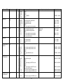
SPECIFICATIONS
• Power
: AC 120V, 50/60Hz
480W (Typical)
5.4A (Maximum)
• Signals
Sync Range
Input Signals
• Input Terminals
RGB
Video
DVD/HD/DTV
Audio
External Control
: Horiz : 15.5 to 93.8 kHZ
(Automatic : step scan)
: Vert : 50.0 to 120 Hz
(Automatic : step scan)
: RGB, HD*1,
DVD*1, DTV*1
: Visual 1 (Analog) : Mini D-sub 15-pin
Visual 2 (Analog) : BNC (R,G,B,H/CS,V)*2
Visual 3 (M-LINK) : MONITORLINKTM
: Visual 1 : RCA-pin
Visual 2 : BNC
Visual 3 : S-Video: DIN 4-pin
: Visual 1 RCA-pin (Y,PB[CB},PR{CR])*1
Visual 2 BNC (Y,PB[CB},PR{CR])*1*
: Stereo RCA x 3 (Selectable)
: D-sub 9-pin (RS232C)
• Sound Output : 7W+7W at 6 ohms
• Dimensions
: (W)49.5" (H)30.2" (D)4.68"
(W)1257 (H)766 (D)119 mm
• Weight
: 98 lbs / 44.5 kg
*1
HD/DVD/DTV Input Signa ls supporte d:
480P (60Hz)
480I (60Hz)
525P (60Hz)
525I (60Hz)
576P (50Hz)
576I (50Hz)
625P (50Hz)
625I (50Hz)
720P (60Hz)
1035I (60Hz)
1080I (50Hz)
1080I (60Hz)
*2
The 5-BNC conne ctors a re use d a s
RGB/PC2 a nd HD/DVD2 input.
Se le ct one of the m unde r "BNC SELECT".
• Weight and dimensions shown are approximate.
• Design specifications are subject to change without notice.
MITSUBISHI DIGITAL ELECTRONICS AMERICA, INC.
9351 Jeronimo Road, Irvine, CA 92618-1904
Copyright © 2002 Mitsubishi Digital Electronics America, Inc.
All Rights Reserved
CONTENTS
SAFETY PRECAUTIONS .................................................................................................................................. 2-1
TROUBLESHOOTING........................................................................................................................................ 3-1
METHOD OF ADJUSTMENTS........................................................................................................................... 4-1
METHOD OF DISASSEMBLY............................................................................................................................ 5-1
PACKAGING....................................................................................................................................................... 6-1
PART LIST.......................................................................................................................................................... 7-1
CONNECTION DIAGRAMS................................................................................................................................ 8-1
BLOCK DIAGRAM.............................................................................................................................................. 9-1
1-1
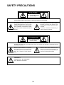
SAFETY PRECAUTIONS
CAUTION
RISK OF ELECTRIC SHOCK
DO NOT OPEN
CAUTION:
TO REDUCE THE RISK OF ELECTRIC SHOCK, DO NOT OPEN REAR COVER. NO USER-SERVICEABLE
PARTS INSIDE. REFER SERVICING TO QUALIFIED SERVICE PERSONNEL.
This symbol warns the user that uninsulated voltage within the unit may have
sufficient magnitude to cause electric
shock. Therefore, it is dangerous to make
any kind of contact with any part inside of
this unit.
This symbol alerts the user that important
literature concerning the operation and
maintenance of this unit has been
included.
Therefore, it should be read carefully in
order to avoid any problems.
ATTENTION
RISQUE D'ELECTROCUTION
NE PAS OUVRIR
ATTENTION:
POUR EVITER LES RISQUES D' ELECTROCUTION, NE PAS ENLEVER LE CONVERCLE ARRÈRE. AUCUN DES
ELEMENTS INTERNES NE DOIT ETRE REPARE PAR L'UTILISATEUR. NE CONFIER L' ENTRETIEN QU'A UN
PERSONNEL QUALIFIE.
L'éclair fléché dans un triangle équilatéral est
destiné à avertir l'utilisateur de la présence,
dans l'appareil, d'une zone non-isolée soumise
à une haute tension dont l'intensité est suffisante pour constituer un risque d'électrocution.
Le point d'exclamation dans un triangle équilatéral est destiné à attirer l' attention de l'utilisateur sur la présence d'informations de
founctionnement et d'entretien importantes dans
la brochure accompagnant l'appareil.
WARNING
HEATSINK MAY BE ENERGIZED.
TEST BEFORE TOUCHING.
2-1
SAFETY PRECAUTIONS
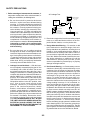
1. Before returning an instrument to the customer, always make a safety check of the entire instrument, including, but not limited to, the following items.
AC Leakage Test
(READING SHOULD
NOT BE ABOVE
3.5 mA)
a. Be sure that no built-in protective devices are
defective and/or have been defeated during
servicing. (1) Protective shields are provided on
this chassis to protect both the technician and
the customer. Correctly replace all missing protective shields, including any removed for servicing convenience. (2) When reinstalling the
chassis and/or other assembly in the cabinet, be
sure to put back in place all protective devices,
including,but not limited to, nonmetallic control
knobs,insulating fishpapers,adjustment and
compartment covers/shields, and isolation resistor/capacitor networks. Do not operate this
instrument or permit it to be operated without all protective devices correctly installed
and functioning.
LEAKAGE
CURRENT
TESTER
DEVICE
UNDER
TEST
+
–
TEST ALL
EXPOSED METAL
SURFACES
3-WIRE CORD
ALSO TEST WITH
PLUG REVERSED
(USING AC ADAPTER
PLUG AS REQUIRED)
EARTH
GROUND
2. Read and comply with all caution and safety-related
notes on or inside the Monitor cabinet, on the Projection Monitor chassis, or on the picture tube.
3. Design Alteration Warning — Do not alter or add
to the mechanical or electrical design of this unit.
Design alterations and additions, including, but not
limited to, circuit modifications and the addition of
the items such as auxiliary audio and/or video output connections might alter the safety characteristics of this Monitor and create a hazard to the user.
Any design alterations or additions will void the
manufacturer's warranty and will make you,the
servicer,responsible for personal injury or property
damage resulting therefrom.
b. Be sure that there are no cabinet openings
through which an adult or child might be able to
insert their fingers and contact a hazardous voltage. Such opening include,but are not limited to,
(1) spacing between the picture tube and the
cabinet mask, (2) excessively wide cabinet ventilation slots, and (3) an improperly fitted and/or
incorrectly secured cabinet back cover.
c. Leakage Current Hot Check — With the instrument completely reassembled,plug the AC line
cord directly into a 240V AC outlet. (Do not use
an isolation transformer during this test.) Use a
leakage current tester or a metering system that
complies with American National Standards Institutes (ANSI) C101.1 Leakage Current for Appliances and Underwriters Laboratories(UL)
1950. With the instrument AC switch first in the
ON position and then in the OFF position, measure from a known earth ground (metal
waterpipe, conduit,etc.) to all exposed metal
parts of the instrument(antennas, handle
bracket, metal cabinet, screwheads, metallic
overlays, control shafts,etc.), especially any exposed metal parts that offer an electrical return
path to the chassis. Any current measured must
not exceed 3.5 milliamp. Reverse the instrument power cord plug in the outlet and repeat
test.ANY MEASUREMENTS NOT WITHIN
THE LIMITS SPECIFIED HEREIN INDICATE A
POTENTIAL SHOCK HAZARD THAT MUST
BE ELIMINATED BEFORE RETURNING THE
INSTRUMENT TO THE CUSTOMER.
4. Hot Chassis Warning — a. Some MultiSync Monitor
chassis are electrically connected directly to one
conductor of the AC power cord and may be safely
serviced without an isolation transformer only if the
AC power plug is inserted so that the chassis is
connected to the ground side of the AC power
source. To confirm that the AC power plug is inserted correctly, with an AC voltmeter measure between the chassis and a known earth ground. If a
voltage reading in excess of 1.0V is obtained, remove and reinsert the AC power plug in the opposite polarity and again measure the voltage potential between the chassis and a known earth ground.
b. Some Plasma chassis normally have 85V AC
(RMS), between chassis and earth ground regardless of the AC plug polarity. These chassis can be
safely serviced only with an isolation transformer
inserted in the power line between the receiver and
the AC power source, for both personnel and test
equipment protection. c. Some Plasma chassis
have a secondary ground systems in addition to the
main chassis ground. This secondary ground system is not isolated from the AC power line. The two
ground system are electrically separated by insulating material that must not be defeated or altered.
2-2
SAFETY PRECAUTIONS
5. Observe original lead dress. Take extra care to
assure correct lead dress in the following areas:
a. near sharp edges, b. near thermally hot parts—
be sure that leads and components do not touch
thermally hot parts, c. the AC supply, d. high voltage, and e. antenna wiring. Always inspect in all
areas for pinched, out-of-place, or frayed wiring. Do
not change spacing between components, and between components and the printed-circuit board.
Check AC power cord for damage.
6. Components,parts, and/or wiring that appear to
have overheated or are otherwise damaged should
be replaced with components, parts, or wiring that
meet original specifications. Additionally,determine
the cause of overheating and/or damage and, if
necessary, take corrective action to remove any
potential safety hazard.
7. PRODUCT SAFETY NOTICE —Many MultiSync
Monitor electrical and mechanical parts have special safety-related characteristics some of which
are often not evident from visual inspection, nor
can the protection they give necessarily be obtained by replacing them with components rated
for higher voltage, wattage, etc. Parts that have
special safety characteristics are identified in this
service data by shading with a mark on schematics and by shading or a mark in the parts list. Use
of a substitute replacement part that does not have
the same safety characteristics as the recommended replacement part in this service data parts
list might create shock, fire, and/or other hazards.
2-3
PRECAUTIONS DE SECURITE
1. Avant de remettre un appareil à un client, faire
toujours d'abord un examen de sécurité de
l'appareil en entier comprenant, mais ne s'y limitant
pas les points cités ci-dessous:
a. Vérifier qu' aucun des dispositifs de protection ne
soit défectueux ou n' ait été endommagé pendant
les travaux.
(1) Les volets protecteurs sur ce châssis ont été
montés pour protéger aussi bien le technicien
que le client. Remplacer correctement tous les
volets protecteurs manquants, aussi bien que
ceux qui ont pu être enlevés pour la commodité
des travaux.
(2) Quand vous remettez le châssis ou d'autres
assemblages ensemble dans le coffret, vérifier
qu' ont été remis à leur place tous les dispositifs
de protection, comprenant mais ne s' y limitant
point, les boutons de contrôle non-métalliques,
les feuilles d'isolation, les couverture/volets de
l'ajustement et du compartiment, et l'isolation des
réseaux résistance/condensateur. Ne pas
travailler sur cet appareil ni permettre qu'y
soit effectué un travail sans que tous les
dispositifs de protection n' y soient
correctement installés fonctionnants.
courant ne doit dépasser 3.5 milliamp. Inverser la
fiche de courant de l'appareil dans la prise et
répéter le test. Tout mesurage ne s'arrêtant
pas aux limites spécifiées icicomporte un risque de décharge électrique dangereux, qui
doit être éliminé, avant que l'appareil ne soit
remis au client.
EXAMEN DE COURANT
D'EXCITATION
(LA MESURE DU COURANT
NE DOIT PAS DEPASSER
3.5 MILLIAMP)
DISPOSIT IF
SOUS
L ' EXAMEN
+
–
VERIFICATEUR
DE CORANT
DE FUITE
EXAMINER TOUTES
LES PIECES METALLIQUES
DEL' APPAREIL EXPOSEE
3-CORDES DE FIL
EXAMINER AVEC
LA FICHE DE COURANT
INVERSEE
(SE SERVIR DE LA FICHE DE COURANT
DE L' A DAPTATEUR COMME DEMANDEE)
PRISE DE TERRE
2. Lire et respecter toutes les mises en garde et notes
de sécurité à l'intérieur ou à l'extérieur du coffret du
rétro-projecteur, sur le châssis du rétro-projecteur
ou sur le tube à images.
b. Bien vérifier qu'il n'y ait aucune ouverture sur le
coffret qui ne puisse permettre à un adulte ou à
un enfant d'y faire pénétrer ses doigts et attraper
une décharge électrique.
De telles ouvertures comprendraient sans pour
autant s'y limiter (1) l'espace entre le tube à images et le coffret de l'eppareil, (2) les espaces
excessivement ouverts pour la ventilation et (3) la
couverture arrière du coffret improprement fixée
ou incorrectement protegée.
3. Mise en garde contre la modification du dessin
Ne pas modifier ni ajouter à la pièce mécanique ou
électrique du modèle. Des modifications ou additions, comportant, mais ne s'y limitant pas, des
modifications des circuits et l'addition d'éléments
tels que des auxilliairs audio et/ou des
branchements pour la prise de vidéo, pourrait
éprouver la sécurité de ce rétro-projecteur et créer
un risque pour l'utilisateur. Tout changement ou addition accomplie annulera la garantie du fabricant et
va rendre votre service d'entretien, responsable des
dommages corporels ou de biens en résultant.
c. Vérification de courant de fuite
L'appareil ayant été complètement réassemblé,
brancher-le à une prise de courant de 240V. (Ne pas se
servir d'un transformateur d'isolation pendant ce
test). Se servir d'un vérificateur de courant
d'excitation ou d'un système de mesure conforme
aux normes ANSI (American National Standards
Institute) C101.1 Leakage Current for Appliances
et U. L (Underwriters Laboratories) 1950. Le bouton de l'appareil en position "Marche" et ensuite
en position "Arrêt", mesurer à partir d'une prise
de terre (métallique tuyauterie, conduite, etc...) à
toutes les pièces métalliques de l'appareil
exposées (antennes, poignet métalliques, coffren
métallique, tête des vis, surfaces métalliques,
traits de contrôle, etc.) surtout à toutes les pièces
métalliques exposées qui peuvent reconduire le
courant au châssis. En aucun cas, la mesure du
4. Mise en garde contre le châssis sous tension
a. Certains châssis de rétro-projecteur sont
électriquement reliés à un conducteur du fil de
courant et ainsi peuvent ne comporter aucun risque sans un transformateur d'isolation seulement
si la prise de courant est branchée, de manière
que le châssis est relié à la prise de terre de la
source de courant. Pour s'assurer que la prise de
courant est correctement insérée, relever les
mesures avec un voltmètre de courant entre le
châssis et un point de prise de terre bien connu.
Si le voltage indiqué est supérieur à 1,0V,
débrancher et reinsérer la prise de courant dans
la polarité contraire et une fois de plus remesurer
le voltage potentiel entre le câssis et la prise de
terre.
2-4
PRECAUTIONS DE SECURITE
b. Certains châssis de moniteur ont habituellement
85V (RMS) entre le châssis et la prise de terre, en
fonction de la polarité de la prise de courant. Ces
châssis peuvent ne comporter aucun risque
seulement avec un transformateur d'isolation
inséré dans la ligne de puissance située entre de
rétro-projecteur et la source d'électricité, cela
pour la protection aussi bien du personnel que du
matériel de vérfication.
c. Certains châssis de rétro-projecteur ont un
système secondaire de masse en addition avec
le système principal de masse du châssis. Ce
système secondaire de masse n'est pas isolé du
courant électrique. Les deux systèmes sont
électriquement séparés par du matériel
d'isolation qu' on vérifiera bien qu'il ne soit ni
altéré ni défectueux.
6. Les composants, parts (pièces) et/ou fils qui ont été
trouvés surchauffés devraient être remplacés avec
les composants, pièces et fils s'y reliant avec d'autre
qui ont les mêmes spécifications que les originales.
De plus, rechercher la cause du surchauffement et/
ou des dommages et si nécessaire, prendre les
mesures propres pour prévenir tout risque potentiel.
7. Note sur sûreté de l'appareil
Beaucoup de pièce de rétro-projecteur, qu'elles
soient électriques ou mécaniques, ont des dispositions de sécurité qui ne sont pas toujours évidentes
d'une simple inspection visuelle et la protection
qu'elles donnent nécessairement ne pourront être
pas obtenues par les remplaçants avec des
composants aux voltages ou watts plus élevés.
Les pièces qui ont des caractéristiques particulières
de sécurité sont identifiées avec un trait
marqué
sur les schémas et sont ombragés ou comportent
un trait
sur la liste des pièces. L'utilisation d'un
produit substitutif qui n'aurait pas les mêmes
caractéristiques comme il est recommandé dans
ces données d'entretien pourrait provoquer une
décharge électrique, un feu, et/ou d'autres dangers.
5. Vérifier la couverture originale en plomb. Accorder
la plus grande attention à la couverture de plomb
notamment aux endroits ci-dessous indiqués.
a. Près des bords aigus
b. près des parties très chaudes
Vérifier que les composants et les plombs ne
touchent pas les parties très chaudes telles que:
c. l'alimentation du courant
d. la haute tension
e. Ies fils de l'antenne
Pousser l'inspection, à tous les endroits, à la recherche des cordes pincées, déplacées ou effilochées.
Ne pas changer l'écartement entre composants, et
entre composants et le tableau de circuit imprimé.
Vérifier que le fil de conduite électrique est en bon
état.
2-5
SAFETY PRECAUTIONS
1 . Cautions for disassembly
(1) For the wall-hang type
During handling, try to support the set
at its frame. Never touch the filter
or glass surface. Assistant personnel on the
front side should apply hands to the lower part
of the casing. [If the casing receives an impact,
the unseen side area of the module panel glass
may be broken even though the module itself does not
seem to have been broken. Therefore, support the
frame by hand in order not to drop it.]
2. The least minimum cautions for product disassembly
Secure a working space, arranged as wide as possible.
Prior to disassembling the set, protect the acrylic
surface with an air mat or the like.
To prevent the thread ridges from being damaged,
use an adequate screwdriver.
Many screws are actually used. Therefore, use
two or three containers where these screws can
be kept . Never disassemble the inner parts of the
module (pipes, etc.).
When lifting the module from the set, two persons
should stand on both sides of the module to hold
the stable parts of the junction while they lift the
module upright. (If dust or such foreign substance
enters in between the module and the filter, moir*
or similar problems can arise. In addition, once it
enters, it is necessary to take careful measures
not to damage the contamination area while removing
contaminants.) [Please understand that the
replacement of the module may call for an air-blast
treatment (air brush) in a clean room.]
Complementary caution) In particular, if a conductive
foreign matter (such as a metallic chip) is attached
to the flexible cable of the module, there
can be danger of the occurrence of a phenomenon
like wire breakage that is caused by partition
breakdown in the module. For this reason, it
is necessary to bear in mind that the flow of air
blast should be directed only in the predetermined
direction at all times.
2-6
SAFETY PRECAUTIONS
(Notes)
The component by the name of “module” used in
this product is defined as a section that is provided with a digital circuit board (including highvoltage parts) used to emit light in the glass panel
part, excluding the surface acrylic fiIter or the tempered glass fiIter. It must be noted that it does
never mean the glass panel part only.
2-7
TROUBLESHOOTING
3-1
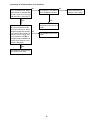
TROUBLESHOOTING
• In the case of abnormality in the POWER system, such as “No power available” or “Alarm (LED flashing)”
Go to → 1. Power failure (P2)
• In the case of abnormality in the VIDEO system, such as “No picture” or “Picture errors”
Go to → 2. No picture displayed, picture errors (P6)
• In the case of no audio output
Go to → 3. No audio output generated (P15)
If set shuts down, reset the microprocessor by pressing the <Power On> and <Input>
keys on the front panel at the same time. Hold for 5 to 6 seconds.
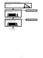
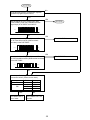
1
1. Power failure
(1) POWER is turned OFF. Note: To Reset the Microprocessor, Press and hold the <Power On> and <Input>
keys on the front panel at the same time. Hold for 5 to 6 seconds.
Turn on the main power unit.
NO
Is the POWER LED lit?
NO
Poor power plug connection
Is the power plug connected
to the wall outlet correctly?
YES
YES
NO
• To “Flashing in green” (2) (P3).
(FAN error detection)
• To “Flashing in red” (3) (P4)
(Temperature error detection)
• To “Flashing in green and red”
(4) (P5).
(Panel crack detection)
Is 100V AC available behind
the fuses F1 and F2?
Fuses F1 and F2 have blown
out.
If the fuses are replaced
and they blow out again,
the POWER unit is out of
order.
YES
NO
Is the M+7V output available
at Pin 1 of the PM connector?
If the PW and RS connectors
are disconnected from one
after another and an output
of M+7V is generated, this
is a problem in a circuit
beyond the connectora.
If no output is generated at
that time, then the POWER
unit is out of order.
YES
NO
Is the M+5V output available
at Pin 2 (MAIN) of IC7005?
From (4): Flashing in green
and red (Panel crack detection)
(P4)
S2601 (PWR) and associated circuits are out of order.
YES
NO
Is the M+5V output available
at Pin 5 of the LD connector,
Pin 4 of the PW connector,
and Pin 5 of the RS connector?
YES
IC7001 and peripheral circuits are out of order.
2
The +5V line is out of order
toward the LED PWB,
PWR, PWB, or 232C PWB.
(Caution) When the LED is flashing (protector in operation), all power lines other than M+7 are automatically
turned off. When checking the power lines other than the M+7V system, a circuit tester or the like
should be connected to the measuring point in advance, for confirmation.
(2) Flashing in green (FAN error detection)
NO
Does the fan run when the main
power supply is turned ON?
NO
Is the power supply available
at Pin 1 of the POF1 and
POF2? (7 to 12V)
YES
IC8802 and peripheral
circuits are out of order.
YES
YES
Is Potential 5V available at
Pin 3 of the POF1 and
POF2?
The fan is out of order,
where Potential 5V is
available. This voltage
becomes 0V when the
power supply is turned off.
Therefore, a circuit tester
should be connected in
advance before inspection.
NO
NO
Is Potential 5V available at
Pin 9 of IC8804?
NO
Is Potential 5V available at
Pin $ of IC8804?
YES
Check IC8804, and also R8807
and R8806.
YES
IC8804 and peripheral
circuit are out of order.
3
VDDM5 and peripheral
circuits are out of order.
(3) Flashing in red (Temperature error detection)
NO
In the cold-start mode, does it
take less than 15 seconds after
the main power circuit is turned
ON and until it is turned OFF?
NO
Is Potential 0V maintained
at Pin 29 (MAIN) of IC7001?
YES
Disconnect the PD, PH, and
AD connectors and turn ON
the main power circuit. Does
the power supply work normally
in this state? (Are normal outputs of D+170V, D+64V, and
D+5V available? Is Pin 3 of
the PM connector maintained at
the [H] level? However, no pictures are displayed.)
YES
TH1 in the POWER unit and
peripheral circuits are out of
order.
NO
The POWER unit is out of
order.
YES
The MODULE and peripheral
circuits are out of order.
4
IC7001 and peripheral
circuits are out of order.
(4) Flashing in green and red (Panel crack detection)
NO
Is Potential 0V maintained at
Pin 100 (MAIN) of IC7001?
IC7001 and peripheral
circuits are out of order.
YES
NO
2
Is Potential 0V maintained at
Pin
(MAIN) of IC7002?
YES
$
Is Potential 5V applied to
Pin
of IC7002?
YES
IC7002 and peripheral
circuits are out of order.
NO
Disconnect the PD, PH, and
AD connectors and turn ON
the main power circuit. Does
the power supply work normally NO
in this state? (Are normal outputs
of D+170V, D+64V, and D+5V
available? Is Pin 3 of the PM
connector maintained at the
[H] level? However, no pictures
are displayed.)
Skip to “ (1) Power is turned
OFF.” (P2).
The POWER unit is out of
order.
YES
The MODULE and peripheral
circuits are out of order.
(Caution) How to cancel the alarm condition:
• While flashing in green and red occurs, the power supply cannot be
reset by ON/OFF operation at the main power switch, remote control,
and wall outlet.
• For alarm resetting, keep pressing the input selector key at the main
unit of the set and move the mains power switch to [ON] at the main
unit. In this state, it is necessary to keep pressing the input selector
key of the main unit for more than 2 seconds.
5
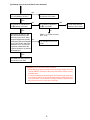
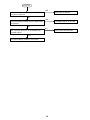
2. No picture displayed and picture errors
(Caution) IPXXXX is installed in the MAIN PWB and the VIDEO PWB. These components are inserted in the
power line. If there is any error occurring in the circuit, these components function to prevent the
evolution of this problem to other areas. Accordingly, check whether the same voltage is generated at
both ends of each component. (In normal state, the component is internally short-circuited.) If the
same voltage is not generated, this means that the MAIN PWB is out of order. The same check is
needed also for the DSP PWB.
(1) No picture display of the PC signal only or both the VIDEO and PC signals
Enter an input of XGA69H gray scale in the input
circuit of PC1, and select PC INPUT 1.
NO
To “No presentation of pictures and ON-screen
display” (P11)
Is ON-screen display available?
YES
YES
Is a signal of 3Vp-p available at at the signal input
pins of IC8701 and IC8702? (Signale names: REV_
LVDS, RODD_LVDS, ets.)
•••
The MAIN PWB of the AD connector is out
of order.
•••
NO
YES
Is a signal of 0.7Vp-p available at Pins 1, 3, 5 of
the PC connector and a sync signal of 5Vp-p
available at Pins 7, 9, 10, 12?
The MAIN PWB is out of order.
1, 3, 5
7, 10
45kHz
9, 12
60Hz
H
V
NO
(1)-1 (P7)
6
(1)-1 (P6)
YES
Are the signals below available at Pins 2, 5, 8, 3,
6, and 9 of the BU connector?
Are the specified voltages available at the
PV connector?
Pin 1 14Vdc
Pin 3 5Vdc
Pin 5 6Vdc
Pin 7 7Vdc
2, 5, 8
5Vp-p
YES
NO
3, 6, 9
The VIDEO PWB is out of order.
5Vp-p
NO
YES
Are the specified voltages available at the
connectors below? (Power source check)
Connector name
PN
PM
Pin No.
1
1
7
9
The MAIN PWB is out of order.
Voltage
3.3Vdc
7Vdc
5Vdc
14Vdc
NO
The POWER unit is out of order.
7
(2) No picture display of the VIDEO signal only
Enter an input of gray scale in the input circuit of VIDEO1,
and select VIDEO1.
YES
Is a signal of about 3Vp-p available at any of
Pins 21 to 79 of the AM connector in the DSP PWB
(GND terminal excluded)?
•••
The MAIN PWB is out of order.
•••
NO
NO
Is a signal of about 3Vp-p available at any of
Pins 101 to 159 of the AM connector in the DSP
PWB (GND terminal excluded)?
•••
The MAIN PWB is out of order.
•••
YES
(2)-1 (P9)
8
(2)-1 (P8)
YES
Are the signals below available at Pins 14 to 17,
19, 98, 96, 95, and Pin 3 (IP8001) of the AM
connector in the DSP PWB?
The DSP PWB is out of order.
14
5Vp-p
15
5Vp-p
16
3Vp-p
17
5Vdc
19
10MHz, 3Vp-p
98
27MHz, 3Vp-p
96
H
15KHz, 3Vp-p
95
V
60Hz, 3Vp-p
3
3Vdc
NO
YES
Is a signal of 1Vp-p available at Pin 1 of the YU
connector, and a sync signal of 5Vp-p available at
Pins 7, 9, 10, and 12?
The MAIN PWB is out of order.
1
7, 10
* 15kHz
9, 12
* 60Hz
* In case of an NTSC input.
H
V
NO
(2)-2 (P10)
9
(2)-2 (P9)
YES
Are the signals below available at Pins 2, 5, 8, 3,
6, and 9 of the BU connector?
Are the specified voltages available at the
PV connector?
Pin 1 14Vdc
Pin 3 5Vdc
Pin 5 6Vdc
Pin 7 7Vdc
2, 5, 8
5Vp-p
YES
NO
3, 6, 9
The VIDEO PWB is out of order.
5Vp-p
NO
YES
Are the specified voltages available at the
connectors below? (Power source check)
Connector name
PN
PM
Pin No.
1
1
7
9
The MAIN PWB is out of order.
Voltage
3.3Vdc
7Vdc
5Vdc
14Vdc
NO
The POWER unit is out of order.
10
No presentation of pictures and
ON-screen display (P6)
NO
Are pulses of 3Vp-p available at Pins 38, 39, and
40 of the AD connector?
YES
NO
Are the horizontal/vertical sync signals of 3Vp-p
available at Pins 27/28 of IC8701, and a clock
signal at Pin 31?
50KHz
60Hz
40MHz
YES
NO
Are the signals of 3Vp-p (signal name: REV_LVDS,
RODD_LVDS, etc.) available at the signal input
pin of IC8701?
YES
YES
Is normal display available when the AD, PD, or
PH cable is replaced?
Each cable is defective.
NO
YES
Is normal display available when the MAIN PWB
is replaced?
The MAIN PWB is out of order.
NO
NO
Are 170V, 64V, and D+5V of the POWER unit
normally output?
See “Power cannot be ON.”
YES
The plasma display module is out of order.
YES
Are the specified voltages available at the
connectors below? (Power source check)
Connector name
PN
PM
Pin No.
1
1
7
9
The MAIN PWB is out of order.
Voltage
3.3Vdc
7Vdc
5Vdc
14Vdc
NO
The POWER unit is out of order.
11
(3) Picture errors
Display a picture in error mode. However, the video signal
level shall be maintained above 0.7Vp-p.
0.7Vp-p or above
YES
NO
Are pulses of 3Vp-p available at Pins 38, 39, and
40 of the AD connector?
YES
NO
Are the horizontal/vertical sync signals of 3Vp-p
available at Pins 27/28 of IC8701, and a clock
signal at Pin 31?
50KHz
60Hz
40MHz
YES
YES
Is a picture error caused by PC input?
Are the specified voltages available at the
connectors below?
(Power source check)
NO
NO
Are the signals below available at Pins 14 to 17,
19, 98, 96, and 95 of the AM connector and at
Pin 3 (IP8001) in the DSP PWB?
Connector name
PN
PM
14
5Vp-p
15
Pin No.
1
1
7
9
YES
Voltage
3.3Vdc
7Vdc
5Vdc
14Vdc
NO
5Vp-p
The MAIN PWB
is out of order.
16
The POWER unit
is out of order.
3Vp-p
17
5Vdc
19
10MHz, 3Vp-p
* Changed according to the input signal.
98
27~37NHz* 3Vp-p
96
H
15~45KHz * 3Vp-p
95
V
50~60Hz * 3Vp-p
YES
3
(3)-1 (P13)
5Vdc
12
(3)-1 (P12)
NO
Does this phenomenon correspond to “Specific
gradations (brightness) are tinted.”?
YES
YES
Are the signals of 3Vp-p (signal name:REV_
LVDS, RODD_LVDS, etc.) available at all the
signal input pin of IC8701 and IC8702?
•••
(3)-2 (P14)
•••
NO
YES
Is a signal of about 3Vp-p available at all Pins 21
to 79 of the AM connector (GND terminals
excluded) in the DSP PWB?
•••
The MAIN PWB is out of order.
•••
NO
YES
Is a signal of about 3Vp-p available at all Pins 101
to 159 of the AM connector (GND terminal excluded)
in the DSP PWB?
•••
The DSP PWB is out of order.
•••
NO
Are the specified voltages available at the
connectors below? (Power source check)
Connector name
PN
PM
YES
The MAIN PWB is
out of order.
Pin No.
1
1
7
9
Voltage
3.3Vdc
7Vdc
5Vdc
14Vdc
NO
The POWER unit is out
of order.
13
(3)-2 (P13)
YES
Is normal display available when the AD, PD, or
PH cable is replaced?
Each cable is defective.
NO
YES
Is normal display available when the MAIN PWB
is replaced?
The MAIN PWB is out of order.
NO
NO
Are 170V, 64V, and D+5V of the POWER unit
normally output?
See “Power cannot be ON.”
YES
The plasma display module is out of order.
14
3. No audio output generated
Note) This model is enabled to set up an audio input terminal for each video input terminal. No audio output is
available unless the input terminal of the displayed pictures (example: VIDEO 1) coincides with that of
audio (example: RGB 3). Therefore, analysis for troubleshooting should be carried out after the displayed
video input terminal (example: VIDEO 1) has been made to coincide with the audio input terminal according to the instruction manual.
Enter a signal input in AUDIO IN.
YES
Is the audio signal present at the speaker OUT?
Speaker or cable is defective.
NO
YES
Are the voltages specified below available at the
PA connector of the AUDIO unit?
(Power source check)
Pin
1
2
3
4
5
6
Signal name
S+24
S+24
S.GND
S.GND
A+13
A.GND
The POWER unit or the cable is out
of order.
Voltage
+23.5~33Vdc
+23.5~33Vdc
GND
GND
+13Vdc
GND
(Note) When confirming the source voltage by disconnecting the PA connector, short-circuit the section between Pins 3 4 of the PA connector and Pin 6 (like short-circuiting between S.GND of the POWER
unit), and then turn on the POWER
unit.
YES
NO
Are the following waveforms observed at the AU
connector of the AUDIO unit?
Pin 6
5Vp-p
Pin 7
5Vp-p
Pin 5
4.8Vdc
The MAIN PWB or the cable is out
of order.
Pin 1, 2 : Audio signal waveforms
YES
The AUDIO unit is out of order.
15
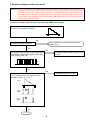
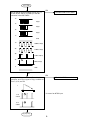
METHOD OF ADJUSTMENTS
4-1
Adjusting conditions
Adjustments should be carried out in accordance with the procedures described below. However, any adjustments
other than the items A & B below are not required.
A. When the [PDP module] is replaced, adjust the sections according to the adjusting items [1 to 3] specified below.
(Caution)
When the PDP module has been replaced, clear the USAGE TIME to “0” without fail, according to
“how to clear the usage time” shown below.
B. When the [POWER unit] is replaced, adjust the sections according to the adjusting items [1 to 3] specified below.
*
How to clear the usage time
Assume the following factory mode by the use of the remote control. Press [MENU/ENTER] key six times
to get the screen [USAGE TIME]. In this state, the integrated time up to the present time is displayed.
The integrated time is cleared to [0] when the remote control keys are pressed in the order of [MUTE] →
cursor keys [ ]→ cursor keys [V] → [SLEEP].
V
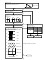
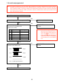
1. Adjustment of +170V
(1) Using any video signal of VIDEO input, DVD/HD input, or RGB input, and display a color bar signal. Turn on
the power switch of the main unit.
(2) Turn the volume control (RV3) in the [D+170V ADJ] section of the power unit, and adjust the voltage value
between TP3 (D+170V output) and TP2 (D.GND) of the power unit so that this voltage settles within the
range of “specified voltage of the PDP module (Value Vs on the label shown below) ± 1V.”
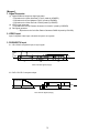
(Caution) The figure below shows a rear side view when the
back cover has been removed.
1
SERIAL NO.
** ** ** ** *
Vd=* *V
Vs=* ** V
CODE
-01
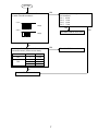
2. Adjustment of +64V
(1) Using any video signal of VIDEO input, DVD/HD input, or RGB input, and display a color bar signal. Turn on
the power switch of the main unit.
(2) Confirm that the voltage at TP4 (D+60V output) and TP2 (D.GND) of the power unit is maintained at a
voltage value (Vd value of the label described in Item 1 above) within ± 1V, specified for the PDP module.
If the voltage specified above cannot be secured, turn the volume control (RV4) in the [D+64V ADJ] block
and adjust the voltage until it attains “the voltage specified for the PDP module (Value Vd on the label of the
above-mentioned Item 1) ± 1V.”
3. Adjustment of +5V
(1) Use any video signal of VIDEO input, DVD/HD input, or RGB input, and display a color bar signal.
(2) Confirm that the voltage value between TP1 (+5V output) and TP2 (D.GND) of the power unit is maintained
at “5.10 ± 0.1V.”
If the voltage specified above cannot be secured, turn the volume control (RV2) in the [D+5V ADJ] block
and adjust the voltage until it attains “5.10 ± 0.1V.”
*
POWER unit layout
TP3
D+170
RV3
D+170
ADJ
PH
PD
TP1
D+5
TP4
D+64
RV4
D+64
ADJ
TP2
D.GND
P
M
P
N
P
V
RV2
D+5 ADJ
P
A
P
I
2
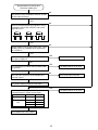
[Morgue]
1. Signal Generator
(1) Digital RGB and component signal generator
• Equivalent to the Video Generator LT1615 (made by LEADER)
• Equivalent to the Panel Adapter LT9217 (made by LEADER)
• Equivalent to the Video Encoder LT1606 (made by LEADER)
(2) NTSC signal generator
• Equivalent to the NTSC Pattern Generator LCG-403YC (made by LEADER)
(3) PAL signal generator
• Equivalent to the Color Bar Pattern Generator PM5518 (made by PHILIPS)
2. VIDEO input
Input: Composite video input or S-terminal input for one system
3. DVD/HD/DTV input
3-1. HD: Y/Pb/Pr component input, tri-sync signal
700
300
350
300
350
Y
Pb
Pr
100% color bar signal (mVp-p)
3-2. DVD: Y/B-Y/R-Y component input
700 (all white)
700
300
Y
Cb
Cr
75% color bar signal (mVp-p)
3
4. RGB/PC input
1)
Horizontal sync period
Video signal
0.7Vp-p
c
d
e
Sync signal
TTL level
b
a
Positive/negative polarity
(2) Vertical sync period
Video signal
0.7Vp-p
h
i
j
Sync signal
TTL level
g
f
Positive/negative polarity
* The data a to j above are specified in the next page and thereafter, classified for various inspection signals.
4
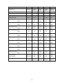
5. RGB/PC signal timing table
PC mode
1
2
3
5
IBM
400@70Hz
PC98
480@60HZ
Signal name
VU-6010
NTSC
Definition
640*240
768*288
640*400
640*400
640*480
Dot clock frequency (MHz)
12.214
14.752
21.053
25.175
25.175
H frequency (kHz)
15.734
15.557
24.826
31.469
31.469
V frequency (Hz)
59.94
50.39
56.423
70.086
59.94
H total (uS)
63.534
64.262
40.285
31.778
31.778
776
948
848
800
800
52.4
52.06
30.4
25.422
25.422
640
768
640
640
640
1.146
1.288
2.803
0.675
0.596
14
19
59
17
15
8.76
8.677
3.04
2.542
3.813
107
128
64
64
96
1.228
2.237
4.037
3.138
1.946
15
33
85
79
49
16.652
20.055
17.723
14.268
16.683
262
312
440
449
525
15.3
18.513
16.112
12.711
15.253
240
288
400
400
480
0.191
0.321
0.282
0.413
0.191
3
5
7
13
6
1.144
1.093
0.322
0.064
0.064
18
17
8
2
2
0.064
0.064
1.007
1.08
1.176
1
1
25
34
37
H sync polarity
Neg
Neg
Neg
Neg
Neg
V sync polarity
Neg
Neg
Neg
Neg
Neg
Interlaced
Interlaced
Non
Interlaced
Non
Interlaced
Non
Interlaced
(dots)
H display period (uS)
(dots)
H front porch (uS)
(dots)
H sync pulse width (uS)
(dots)
H back porch (uS)
(dots)
V total (mS)
(line)
V display period (mS)
(line)
V front porch (mS)
(line)
V sync pulse width (mS)
(line)
V back porch (mS)
(line)
Scan type
VU-6010
PC98
PAL/SECAM 400@56Hz
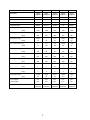
4
5
PC mode
6
7
8
9
10
MAC@13”
VESA
480@72Hz
VESA
480@75Hz
VESA
480@85Hz
XGA-2
480@75HZ
640*480
640*480
640*480
640*480
640*480
30.24
31.5
31.5
36.0
31.5
H frequency (kHz)
35
37.861
37.5
43.269
39.375
V frequency (Hz)
66.667
72.809
75
85.008
75
H total (uS)
28.571
26.413
26.667
23.111
25.4
864
832
840
832
800
21.164
20.317
20.317
17.778
20.32
640
640
640
640
640
2.116
0.762
0.508
1.556
0.508
64
24
16
56
16
2.116
1.27
2.032
1.556
3.048
64
40
64
56
96
3.175
4.064
3.81
2.222
1.524
96
128
120
80
48
15
13.735
13.333
11.764
13.333
525
520
500
509
525
13.714
12.678
12.8
11.093
12.19
480
480
480
480
480
0.086
0.237
0.027
0.023
0.279
3
9
1
1
11
0.086
0.079
0.08
0.069
0.051
3
3
3
3
2
1.114
0.739
0.427
0.578
0.813
39
28
16
25
32
H sync polarity
Sync on G
Neg
Neg
Neg
Neg
V sync polarity
Sync on G
Neg
Neg
Neg
Neg
Scan type
Non
Interlaced
Non
Interlaced
Non
Interlaced
Non
Interlaced
Non
Interlaced
Signal name
Definition
Dot clock frequency (MHz)
(dots)
H display period (uS)
(dots)
H front porch (uS)
(dots)
H sync pulse width (uS)
(dots)
H back porch (uS)
(dots)
V total (mS)
(line)
V display period (mS)
(line)
V front porch (mS)
(line)
V sync pulse width (mS)
(line)
V back porch (mS)
(line)
6
PC mode
11
12
13
14
15
VESA
600@56Hz
VESA
600@60Hz
VESA
600@72Hz
VESA
600@75Hz
VESA
600@85Hz
800*600
800*600
800*600
800*600
800*600
36
40
50
49.5
56.25
H frequency (kHz)
35.156
37.879
48.077
46.875
53.674
V frequency (Hz)
56.25
60.317
72.188
75
85.061
H total (uS)
28.444
26.4
20.8
21.333
18.631
1024
1056
1040
1056
1048
22.222
20
16
16.162
14.222
800
800
800
800
800
0.667
1
1.12
0.323
0.569
24
40
56
16
32
2
3.2
2.4
1.616
1.138
72
128
120
80
64
3.556
2.2
1.28
3.232
2.702
128
88
64
160
152
17.778
16.579
13.853
13.333
11.756
625
628
666
625
631
17.067
15.84
12.48
12.8
11.179
600
600
600
600
600
0.028
0.026
0.77
0.021
0.019
1
1
37
1
1
0.057
0.106
0.125
0.064
0.056
2
4
6
3
3
0.626
0.607
0.478
0.448
0.503
22
23
23
21
27
H sync polarity
Pos.
Pos.
Pos.
Pos.
Pos.
V sync polarity
Pos.
Pos.
Pos.
Pos.
Pos.
Non
Interlaced
Non
Interlaced
Non
Interlaced
Non
Interlaced
Non
Interlaced
Signal name
Definition
Dot clock frequency (MHz)
(dots)
H display period (uS)
(dots)
H front porch (uS)
(dots)
H sync pulse width (uS)
(dots)
H back porch (uS)
(dots)
V total (mS)
(line)
V display period (mS)
(line)
V front porch (mS)
(line)
V sync pulse width (mS)
(line)
V back porch (mS)
(line)
Scan type
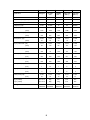
7
PC mode
16
17
18
19
20
MAC@16”
I/O dater
wide
CEREB
wide 1
VESA wide
(NEC 1)
VESA wide
(NEC 2)
Definition
832*624
852*480
864*480
848*480
1024*576
Dot clock frequency (MHz)
57.2832
34.006
42.526
33.75
47.25
H frequency (kHz)
49.725
31.722
37.5
31.02
35.795
V frequency (Hz)
74.55
59.966
75
60
60.059
H total (uS)
20.111
31.524
26.667
32.237
27.937
1152
1072
1134
1088
1320
14.524
25.055
20.317
25.126
21.672
832
852
864
848
1024
0.559
0.659
0.508
0.474
0.339
32
22
22
16
16
1.117
3.764
2.032
3.319
3.048
64
128
86
112
144
3.91
2.047
3.81
3.319
2.878
224
70
162
112
136
13.414
16.676
13.333
16.667
16.65
667
529
500
517
596
12.549
15.132
12.8
15.474
16.091
624
480
480
480
576
0.02
0.378
0.027
0.193
0.056
1
12
1
6
2
0.06
0.095
0.08
0.258
0.112
3
3
3
8
4
0.784
1.072
0.427
0.741
0.391
39
34
16
23
14
H sync polarity
Sync on G
Neg
Pos.
Pos.
Pos.
V sync polarity
Sync on G
Neg
Neg
Pos.
Pos.
Scan type
Non
Interlaced
Non
Interlaced
Non
Interlaced
Non
Interlaced
Non
Interlaced
Signal name
(dots)
H display period (uS)
(dots)
H front porch (uS)
(dots)
H sync pulse width (uS)
(dots)
H back porch (uS)
(dots)
V total (mS)
(line)
V display period (mS)
(line)
V front porch (mS)
(line)
V sync pulse width (mS)
(line)
V back porch (mS)
(line)
8
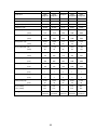
PC mode
21
22
23
24
25
VESA wide
(NEC 3)
VESA wide
(NEC 4)
CEREB
wide 2
VESA
768@60Hz
VESA
768@70Hz
1280*720
1360*768
1024*600
1024*768
1024*768
76.5
85.5
51.2
65
75
H frequency (kHz)
45.106
47.712
37.879
48.363
56.476
V frequency (Hz)
60.142
60.015
60.317
60.004
70.069
H total (uS)
22.17
20.959
26.4
20.677
17.707
1696
1792
1352
1344
1328
16.732
15.906
20
15.754
13.653
1280
1360
1024
1024
1024
0.627
0.749
1
0.369
0.32
48
64
51
24
24
2.301
1.310
3.2
2.092
1.813
176
112
164
136
136
2.51
2.994
2.2
2.462
1.92
192
256
113
160
144
16.627
16.662
15.579
16.666
14.272
750
795
628
806
806
15.962
16.097
15.84
15.88
13.599
720
768
600
768
768
0.089
0.063
0.026
0.062
0.053
4
3
1
3
3
0.177
0.126
0.106
0.124
0.106
8
6
4
6
6
0.399
0.377
0.607
0.6
0.513
18
18
23
29
29
H sync polarity
Pos.
Pos.
Neg
Neg.
Neg.
V sync polarity
Pos.
Pos.
Pos.
Neg.
Neg.
Non
Interlaced
Non
Interlaced
Non
Interlaced
Non
Interlaced
Non
Interlaced
Signal name
Definition
Dot clock frequency (MHz)
(dots)
H display period (uS)
(dots)
H front porch (uS)
(dots)
H sync pulse width (uS)
(dots)
H back porch (uS)
(dots)
V total (mS)
(line)
V display period (mS)
(line)
V front porch (mS)
(line)
V sync pulse width (mS)
(line)
V back porch (mS)
(line)
Scan type
9
PC mode
26
27
28
VESA
768@75Hz
VESA
768@85Hz
MAC@19”
1024*768
1024*768
1024*768
1280*1024
1280*1024
Dot clock frequency (MHz)
78.75
94.5
80
108
135
H frequency (kHz)
60.023
68.677
60.24
63.981
79.976
V frequency (Hz)
75.029
84.997
74.93
60.02
75.025
H total (uS)
16.66
14.561
16.600
15.63
12.501
1312
1376
1328
1688
1688
13
10.836
12.8
11.852
9.481
1024
1024
1024
1280
1280
0.203
0.508
0.4
0.444
0.119
16
48
32
48
2
1.219
1.016
1.2
1.037
1.067
96
96
96
112
144
2.235
2.201
2.2
2.296
1.837
176
208
176
248
248
13.328
11.765
13.347
16.661
13.329
800
808
804
1066
1066
12.795
11.183
12.749
16.005
12.804
768
768
768
1024
1024
0.017
0.015
0.050
0.016
0.013
1
1
3
1
1
0.05
0.044
0.050
0.047
0.038
3
3
3
3
3
0.466
0.524
0.498
0.594
0.475
28
36
30
38
38
H sync polarity
Pos.
Pos.
—
Pos.
Pos.
V sync polarity
Pos.
Pos.
—
Pos.
Pos.
Non
Interlaced
Non
Interlaced
Non
Interlaced
Non
Interlaced
Non
Interlaced
Signal name
Definition
(dots)
H display period (uS)
(dots)
H front porch (uS)
(dots)
H sync pulse width (uS)
(dots)
H back porch (uS)
(dots)
V total (mS)
(line)
V display period (mS)
(line)
V front porch (mS)
(line)
V sync pulse width (mS)
(line)
V back porch (mS)
(line)
Scan type
10
29
30
VESA
VESA
1024@60Hz 1024@75Hz
PC mode
31
32
33
34
35
IDC-3000G
PAL 625P
IDC-3000G
NTSC 525P
HDTV-J
DTV (480P)
DTV (720P)
768*576
640*480
1920*1034
644*483
1280*720
Dot clock frequency (MHz)
29.687
24.39
74.25
24.37
74.25
H frequency (kHz)
31.389
31.47
33.75
31.469
45.000
V frequency (Hz)
50
59.9
60/60
59.94
60
31.933
31.775
29.63
31.777
22.222
948
775
2200
774
1650
25.87
26.24
25.86
26.427
17.239
768
640
1920
644
1280
0.269
0.41
0.59
0.75
0.943
8
10
44
18
70
2.526
2.46
0.59
2.35
1.077
75
60
44
57
80
3.267
2.665
2.59
2.25
2.963
97
65
192
55
220
19.911
16.522
16.652
16.683
16.667
625
525
562/562
525
750
18.35
15.106
15.319
15.348
576
480
517/517
483
720
0.223
0.252
0.148
0.191
0.111
7
8
5
6
5
0.223
0.22
0.148
0.191
0.111
7
7
5
6
5
1.115
0.944
1.037
0.953
0.444
35
30
35
30
20
H sync polarity
Neg
Neg
Neg
Neg
Neg
V sync polarity
Neg
Neg
Neg
Neg
Neg
Non
Interlaced
Non
Iinterlaced
Interlaced
Non
Interlaced
Non
Interlaced
Signal name
Definition
H total (uS)
(dots)
H display period (uS)
(dots)
H front porch (uS)
(dots)
H sync pulse width (uS)
(dots)
H back porch (uS)
(dots)
V total (mS)
(line)
V display period (mS)
(line)
V front porch (mS)
(line)
V sync pulse width (mS)
(line)
V back porch (mS)
(line)
Scan type
11
PC mode
36
37
38
39
HDTV-W
SSPE
JSPE
MAC@12”
1920*1080
1024*512
852*480
1152*870
Dot clock frequency (MHz)
74.25
40
16
100
H frequency (kHz)
33.75
33.727
15.75
68.681
V frequency (Hz)
60/60
60.012
59.94
75.062
H total (uS)
29.630
29.650
63.750
14.560
2200
1186
1020
1456
25.859
25.600
53.250
11.520
1920
1024
852
1152
0.593
0.600
1.250
0.320
44
24
20
32
1.185
1.200
4.750
1.280
88
48
76
128
1.993
2.250
4.500
1.440
148
90
72
144
16.652/16.682
16.663
16.683
13.322
562/563
562
262.5/262.5
915
16.000/16.000
15.15
15.236/15.236
12.667
540/540
511
239/239
870
0.059/0.074
0.178
0.064/0.096
0.044
2/2.5
6
1/1.5
3
0.148/0.148
0.148
0.191/0.191
0.044
5/5
5
3/3
3
0.444/0.459
1.186
1.211/1.243
0.568
15/15.5
40
19/19.5
39
H sync polarity
Neg
Neg
Neg
Sync on G
V sync polarity
Neg
Neg
Neg
Sync on G
Interlaced
Non
Interlaced
Interlaced
Non
Interlaced
Signal name
Definition
(dots)
H display period (uS)
(dots)
H front porch (uS)
(dots)
H sync pulse width (uS)
(dots)
H back porch (uS)
(dots)
V total (mS)
(line)
V display period (mS)
(line)
V front porch (mS)
(line)
V sync pulse width (mS)
(line)
V back porch (mS)
(line)
Scan type
12
METHOD OF DISASSEMBLY
(Cautions)
1. Before disassembly, turn power off the main unit and pull out the power plug from the wall outlet.
2. Use a screwdriver with a fitting size. Otherwise, the screw threads may be damaged.
3. Reassembly can be carried out in the reverse order for disassembly. Refer to the disassembly procedures and
forward reassembly in the reverse order.
4. The order for taking out the parts (or components) is indicated by the foregoing numeral that is attached to the
name of each part (or component).
5. The wire connector symbol is indicated by two digits of Marking
. Read CNwhen examining the table
of parts.
5-1
1.LABEL
SUPPLEMENT SHEET (M62)
FILAMENT TAPE(9mm*50m)
NAME PLATE(M53)
SPEAKER LABEL(M54)
LABEL (EARTH) (M65)
SERIAL LABEL(M10)
LABEL A (2001) (M66)
LABEL (OUT) (M64)
AC IN LABEL(M55)
5
2.BACK COVER
(1)PL-CPIMS*4*12*15KF(SRW36)
FELTSHHET(M69)
STAND REAR SIDE
TERMINAL LABEL B (M57)
(3) BACK COVER (M58)
(2)PL-CPIMS*3*6*3KF(SRW35)
3 GASKET L=200
1 GASKET L=50
4 GASKET L=250
3 GASKET L=200
5 GASKET L=290
1 GASKET L=50
SCREW(M68)
024N04431 *6
BACK COVER REAR SIDE
SYMBOL
3
PARTS NAME
PARTS NO. Q'TY
1 (GSK03) GASKET (L50*10*T7)
4
2 (GSK04) GASKET (L200*10*T7)
5
3 (GSK05) GASKET (L290*10*T7)
1
4 (GSK06) GASKET (L250*10*T7)
4
5 (GSK07) GASKET (L100*10*T7)
1
4 GASKET L=250
GASKET L=200
4
3 GASKET L=200
GASKET L=250
BACK COVER
3.MAIN PWB/DSP PWB/VIDEO PWB
GASKET (L160*9*T4) (M19 (GSK11))
(1)TP-M4*8*3KF(SRW34)
*2
2 GASKET L=100
1 GASKET L=50
TP-M4*8*3KF(SRW11,12)
3 GASKET L=200
4 GASKET L=250
1 GASKET L=50
GASKET (L150*10*T4) (M20
(GSK13)) *2
*4X2
BRACKET (FAN) L (M36)
FAN MOTOR(E01)
GASKET (L200*10*T7) (M12 (GSK04))
*2
*2
(4) SHIELD COVER (MAIN/VIDEO) (M43)
SCREW,M3*30*15KF(SRW29)
*2X2
BRACKET (FAN) R (M37)
(2) BRACKET (OPTION L) (M42)
GASKET(L300*10*T7)(M20(GSK12))
(3)TP-M3*6*3KF(SRW33)
TP-M4*8*3KF(SRW30)
*8
*2
COVER(BOTTOM)(M29)
*2
TP-M4*8*3KF(SRW28)
*1X2
GASKET(L70*10*T1)(M18(GSK10)
*2X2
TP-M4*8*3KF(SRW31)
(Caution) When mounting a back
*4X2
cover, stick the filament tape
BRACKET STAND(A)(M30)
(30mm*50m) for the
*2
prevention of getting flaws.
In this case, however, the filament
TP-M4*8*3KF(SRW32)
tape shall be removed after
mounting.
BUTTON(PWR)(M07)
*2X2
COVER(POWER SW)(M26)
PWR PWB ASSY(PWC-4419C)(A10)
BRACKET STAND(B)(M31)
*2
1
(Caution) At the time of assembly, it shall
EDGE SADDLE(M06)
(5)TP-M4*8*3KF(SRW13)
*3
*6
be tightened together with the round
terminal of the connector CN-AD.
(6) TERMINAL PANEL (VI) ASSY (M59)
Adhesion of the protective tape
TP-M4*8*3KF(SRW34)
(Caution) When mounting a back
BRACKET (OPTION R) (M44)
cover, stick the filament tape
*2
(30mm*50m) for the
TERMINAL PANEL (232) ASSY (M60)
TP-M3*6*3KF(SRW19)
prevention of getting flaws.
*2
In this case, however, the filament
PANEL PWB ASSY (PCB-5023B) (A03)
tape shall be removed after mounting.
SCREW(UNC4-40/4-40)(SRW241)
*2
PL-CPIMS*3*6*3KF(SRW15)
*2
C/L BUTTON(M08)
TP-M3*6*3KF(SRW20)
*4
PL-CPIMS*3*6*3KF(SRW202)
232C PWB ASSY (PWC-4419A) (A08)
*2
• TERMINAL PANEL (VI) ASSY
(8) MAIN PWB ASSY (PCB-5022) (A01)
(7)TP-M3*6*3KF(SRW16,162)
(12)TP-M3*6*3KF(SRW17)
*9
*5
[C]
(9) DSP PWB ASSY (PCB-5022) (A06)
(13) VIDEO PWB ASSY(PCB-5023A) (A02)
SHIELD PLATE (VIDEO) (M46)
[A]
[D]
[C]
[D]
[B]
(11) 6SCREW (UNC4-40/4-40) (SRW106)
(10) CBIPS*3*8*3KF (SRW18)
*2
*9
CUSHION RUBBER(M70)
*2
[B]
[A]
2
4. AUDIO AMPLIFIER MODULE
SP PWB ASSY (PWC-4419E) (A12)
LED PWB ASSY (PCB-4419B) (A11)
TERMINAL PANEL (SP) (M61)
TP-M3*6*3KF(SRW24)
*2
CBIPS*4*12*3KF (SRW02)
*3
TP-M4*8*3KF(SRW37)
CBIPS*3*8*3KF(SRW23)
*4
*2
CTL PWB ASSY (PCB-4419B) (A09)
(1)TP-M3*6*3KF(SRW21)
*2
GASKET (L70*10*T1) (M17 (GSK09))
*2
MESH (M47)
(3)AUDIO AMPLIFIER MODULE(A_UNIT)
(2)SCREW,P-CPIMS*3*14*3KF(SRW22)
*2
• AC INLET ASSY
ET-CBIMS*4*8*3KF(SRW26)
CABLE 1P(E02) 07S530015 Green
CABLE
Blue
2P
(E02)
CABLE 2P(E02) Brown
AC INLET 10GEEG3C(E02)
(Caution) No bending process
TP-M4*8*3KF(SRW27)
COVER (INLET) (M63)
*2
Rear side of the set
Rear side of the set
GASKET (L60*10*T2) (M17 (GSK08))
Insulation tube
*2
Lock
release
terminal
Hook
Front side of the set
BARRIER (INLET) (M09)
Lock hole button side
PL-CPIMS*3*10*15KF(SRW25)
(Caution) Insert the cable in the AC inlet until its terminal hook is locked.
After insertion, try to pull the cable to confirm whether or not
it comes out. To disconnect the cable, push the lock release
terminal by a finger in the direction of the arrow, and pull out
the cable in the lengthwise direction. (No unlocking unless the
position of hook's tip is lower than the lock hole bottom side.)
Side view
3
*2
5. POWER UNIT
TP-M4*8*3KF(SRW39,40)
*2 x 2
SENS PWB ASSY(PCB-5023C)(A04)
PLATE(M48)
*2
SENT PWB ASSY(PCB-5023D)(A05)
SENS PWB ASSY
PLATE
SENT PWB ASSY
(2)BRACKET(POWER)(M41)
INSULATORD4.5*T1)(M67)
(3) TP-M4*8*3KF (SRW09)
(4)POWER UNIT(A13)
*6
*6
(1)TP-M4*8*3KF(SRW10)
*7
6.PDP MODULE
(11)FRAME(T)(M34)
(10)TP-M4*8*3KF(SRW07)
*2
(4)TP-M4*8*3KF(SRW04)
CN 9P(PH)(CN-PH)
CN 10P(PD) (CN-PD)
*8
STOP UP SHEET(M71)
*8
(6)TP-M4*8*3KF(SRW05)
(1)PL-CPIMS*4*16*3GF(SRW03)
*9
*4 x 2
(5)BRACKET(L)(M32)
(7)BRACKET(R)(M33)
FRAME(L)
FRAME(R)
STOP UP SHEET
(2)FRAME(L) (M27)
(3)FRAME(R) (M28)
(M71)
*8
(12)TP-M4*8*3KF(SRW06)
(9) FRAME(CENTER)(M45)
*4
(13)FRAME(B)(M35)
(8) TP-M4*8*3KF(SRW08)
*2
4
(8) TP-M3*6*3KF(SRW38)
CLAMPER, WIRE (M04)
(Caution)
Make a connection
where no "AD" label
is present.
(14) PDP-NP50C2MF01 (P01)
TAPE 1150mm*2
(30m)
7.FRONT PANEL ASSY/FILTER
(2) BRACKET FILTER (T) (M38)
(1)CBIPS*4*12*3KF(SRW01)
*16
(3)BRACKET FILTER(S)(M40)
*2
*
TAPE 680mm x 2
*
(30m)
(2) CUSHION (10*5*600) (M49)
(4) BRACKET FILTER (B) (M39)
A=10 ± 5mm
A
A
SPACER(FILTER)(M51)
(5) FILTER(M52)
*4
(6)FRONT PANEL ASSY(M01)
A
Reference position
5
WIRING DIAGEAM
5 Wind the TR by one turn
1 Fix the PD, PH
Fixed to the vicinity of the sensor PWB
Delete the TR
1 Fix the FAN, PD
3 Fix the surplus
PD
PD
part of the fan
1 Fix the AD
1 Fix the PH
1 Fix the PD, PH
5 Pass the AD
5 Wind the TM by one turn Fixed to the vicinity of the sensor PWB
6 *3 Pass the PD, PH
TR
4 Fix the surplus part of the fan
TM
5 Add the X2
Pass the TM, TR
Allocate each to the upper
and lower sides of the PD
and PH cables.
The cables shall be passed
between the core 6 and the
clamper 1 .
5 Pass the AD in the vicinity of
the digital PWB of the module
PH
PD
PN
PV
PA
1 Fix the fan, TR,
PH, and PD twice
5 Pass the PV
5 Pass the PN
F1
SY
DS
2 PN, PV, PA, PM
PL
SY
PM
1 Fix the AD
5 X2
F2 AD
TR
F3
TM
5 Pass the YU
PM
Pass the LD, PW
BU
PN
YU
LD
PC
PW
AQ SW RS BU
2 Fix the PV, PA, LD, PW
8 Wind the green wire by two turns
1 Fix the green wire
YU
1 BU, AU, PV,
PC
PV AQ AU
RS, SW
5 Pass the AQ and fix it
AC
by the use of the harness
band attached
PL
RM LM
AU PA
5 Pass the RS
RS
PW
LM RM
SW
LE
LD
LE
Hook the LE on the LD
1 Fix the LD, PW
5 Wind the green
wire by one turn
6 Pass the AC
1 Fix the LM, RM
line and the
green wire
6 Give two turns to the
8 Fix the AC line by
means of a winding
lug so that it cannot
come off the chassis
5 Pass the PC
1 *2 Fix the AU, PA
6 Wind the PA by one turn
LM and RM assembled 1 Fix the PV, PA, AQ, SW, RS BU
together
1 Fix the LD, PW
(Caution) Fix the AC cable by means of a winding lug to
reduce the cable height so that it cannot come
in contact with the back cover.
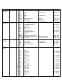
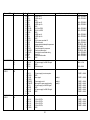
SYMBOL
PARTS NAME
— CN-AD CABLE 41P L250
— CN-AQ CN 4P(AQ) 400W,2791-28
— CN-AU CN 7P(AU) 500W,2791-28
PART No.
Q'ty
SYMBOL
PARTS NAME
PART No.
Q'ty
1
1
M02 CLAMPER,WIRE
1
2
M03 CLAMPER,WIRE (D11.5)
2
1
3
M05 CLAMPER,WIRE (D8.3)
1
1
4
15
— CN-BU CN 14P(BU) 325W,2468-26
— CN-DS CN 3P(DS) 50S, 1007-26
— CN-LD CN 5P(LD) 625W,2468-26
M21 LEAD CLAMPER (D5.2)
1
1
5
FL31 FERRITE CORE ZCAT2032-930(FG)
1
1
5
FL12 FERRITE CORE ZCAT2032-930(AD)
2
— CN-LE CN 5P(LE) 125,2468-26
1
5
FL35 FERRITE CORE ZCAT2032-930(TM)
1
— CN-LM CN 3P(LM) 400,2468-26
1
5
FL36 FERRITE CORE ZCAT2032-930(TR)
1
5
FL5 FERRITE CORE ZCAT2032-930(PN)
1
5
FL6 FERRITE CORE ZCAT2032-930(RS)
FL8 FERRITE CORE ZCAT2032-930(PC)
1
— CN-PA CN 6P(PA) 700,2468-26
— CN-PC CN 13P(PC) 125W,MIX
— CN-PD CN 10P(PD) 900W, 1007-20
— CN-PH CN 9P(PH) 500W, 1007-20
— CN-PL CABLE, TWINAX 21P L450
— CN-PM CN 11P(PM) 100W,2468-26
— CN-PN CN 10P(PN) 150W,2468-26
— CN-PV CN 8P(PV) 600W,2468-26
— CN-PW CN 6P(PW) 650W,2468-26
— CN-RM CN 2P(RM) 375,2468-26
— CN-RS CN 9P(RS) 475W,2468-26
— CN-SW CN 3P(SW) 625W,2468-26
1
1
1
5
5
1
1
5
FL37 FERRITE CORE ZCAT2032-930(LD/PW)
FL38 FERRITE CORE ZCAT2032-930(LD/PW)
1
5
FL51 FERRITE CORE ZCAT2032-930(PV)
1
1
5
1
5
FL52 FERRITE CORE ZCAT2032-930(AQ)
FL53 FERRITE CORE ZCAT2032-930(YU)
5
FL54 FERRITE CORE ZCAT2032-930(TR'/TM')
2
6
FL30 FERRITE CORE SFT-72SB (AC FG)
1
6
FL11 FERRITE CORE SFT-72SB (PA)
FL33 FERRITE CORE SFT-72SB (LM,RM)
1
6
1
6
FL7 FERRITE CORE SFT-72SB (PD/PH)
3
7
FL32 FERRITE CORE (ESD-R-19) (FG)
1
8
M72 LUG (L72)
1
1
1
1
1
1
1
— CN-SY CN 5P(SY) 175W,1691-28
— CN-TM CN 4P(TM) 525W,2468-26
1
— CN-TR CN 4P(TR) 525W,2468-26
— CN-YU CN 12P(YU) 125W,MIX
1
1
1
6
1
1
1
PACKAGING
6-1
1.BAG A
BRACKET(SAFE)
BAG
PL-CPIMS*4*10*3KF
BAG
2.BAG B
BAG
SERVICE STATION GUIDE
NOTICE SHEET
USER'S MANUAL
SUPPLEMENT SHEET
3.BAG C
BAG,POLYETHYLENE(150*370)
BAG B
PLUG
BATTERY,DRY CELL UM-4*2
CORE,FERRITE
FERRITE CORE
1
4. ACCESSORY BOX
BAG B
PLUG CABLE
BAG
REM-T HAND UNIT
POWER CORD
CABLE,D-SUB 15P L1800
BAG C
ACCESSORY BOX
2
5.CARTON BOX
FRONT
BAR CODE SERIAL LABEL
PILLER T
SPACER TR
SPACER TL
PROTECTION SHEET
PILLER S
SPACER BR
SPACER BC
ACCESSORY BOX (W)
SPACER BL
CARTON BOX B
PILLER S
PILLER T
PROTECTION SHEET
TAPE
3
STOPPER
TAPE
PP BAND
JOINT
BAR CODE SERIAL LABEL
BACK
4
PARTS LIST
Notes:
1. Parts orders must contain model name, parts number and parts name.
2. When you place an order for spare parts, please refer to the respective service manual and mention the right
parts number on your P.O. sheets
3. The letters NSP in the table indicate non-service parts.
4. Please refer to METHOD OF DISASSEMBLY or PACKAGING of service manual about a parts layout.
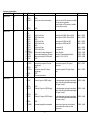
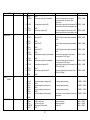
Part Number
03S130222
07S530015
07S530021
07S530008
07S580006
07S580010
07S530002
07S552004
029P00812
03S170001
029H00024
029H00034
029K00351
I/B PD5010
029DS0411
029PS0821
029PS0621
09S900017
0936P7D01
0936P7M01
03S110061
0936P7S91
0936P7V01
03S120141
PD-5010 Parts List
Description
AUDIO AMPLIFIER MODULE
CABLE-1P L360
CABLE-2P L240
CABLE-41P L250
CABLE-D-SUB 15P L1800
CABLE-STEREO MINI L3M
CABLE-TWINAX 21P L450
CORD-POWER AC
COVER-BACK ASSY
FAN-MOTOR (109P1212L4D03)
FRAME (L)
FRAME (R)
FILTER-SCREEN SHIELD (M52)
INSTRUCTION BOOK
PANEL-FRONT ASSY (M01)
PANEL-TERMINAL (232) ASSY
PANEL-TERMINAL (VI) ASSY
PDP-NP50C2MF01
PWB-DSP ASSY (PCB-5015)
PWB-MAIN (PCB-5022)
PWB-POWER UNIT (A13)
PWB-SUB ADJ (PWC-4419A)
PWB-VIDEO (PCB-5023A)
REM0TE
7-1
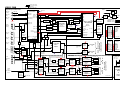
CONNECTION DIAGRAMS
8-1
PD-5010 BLOCK DIAGRAM
SW7
POIN
GND
M+5V
M+7V
NC
1
2
3
4
5
6
PW
PW
1
2
3
4
5
6
SW7
POIN
D.GND
M+5V
M+7V
NC
AQ
WR
1
2
3
4
5
6
7
8
9
10
11
12
GOUT
A.GND
BOUT
A.GND
ROUT
A.GND
PCMHD
A.GND
PCMVD
PCHD
A.GND
PCVD
A.GND
1
2
3
4
5
6
7
8
9
10
11
12
13
PC
1
2
3
4
SCL5
SDA5
A+5V
D.GND
1
2
3
4
5
6
7
8
9
10
11
12
YOUT
GND
UOUT
GND
VOUT
GND
YUMHD
GND
YUMVD
YUHD
GND
YUVD
1
2
3
4
5
6
7
8
9
10
11
12
13
GOUT
GND
BOUT
GND
ROUT
GND
PCMHD
GND
PCMVD
PCHD
GND
PCVD
GND
PV
AU
PANEL PWB
(PCB-5023B)
RS
1
2
3
4
5
6
AU_L
GND
AU_R
GND
POMUTE
SCL4
SDA4
S+25V
S+25V
GND
GND
A+14V
GND
GND
AUDIO AMP MODULE
1
WOOFEROUT 2
3
SMUTE
4
GND
WE
1
2
3
4
5
6
7
AU
PA
GND
LOUT
GND
ROUT
GND
1
2
3
LM
1
2
RM
1
2
3
GND
LOUT
GND
1
2
ROUT
GND
AQ
PL
RS
REMIN1
LEDCTL1
LEDCTL2
GND
M+5V
LED PWB
(PWC-4419D)
VIDEO PWB
(PCB-5023A)
SDA4
SCL4
POMUTE
GND
SCL5
SDA5
A+5V
GND
A+12
GND
FSIG
1
2
3
1
2
3
A+12
D.GND
FSIG
SW
YOUT
A.GND
UOUT
A.GND
VOUT
A.GND
YUMHD
A.GND
YUMVD
YUHD
A.GND
YUVD
YU
PC3HD
GND
PC3VD
GND
NC
1
2
3
4
5
LE
1
2
3
4
1
2
3
4
5
6
7
8
9
D+170
D+170
NC
D+70
GND
GND
D+5
GND
GND
158
159
160
1
2
3
4
5
6
7
8
9
10
11
12
13
14
1
2
3
4
5
1
2
3
4
REMIN1
LEDCTL1
LEDCTL2
D.GND
M+5V
DSP PWB
PCB-5015
1
2
3
4
.
.
.
NC
SCL3
SDA3
D.GND
SCL7
SDA7
D.GND
SCL8
SDA8
D.GND
POSYNC
HDSTOP
SMODE
D.GND
NC
SCL3
SDA3
GND
SCL7
SDA7
GND
SCL8
SDA8
GND
POSYNC
SDET
SMODE
GND
A+14V
GND
A+5V
GND
M+6A
GND
M+7V
GND
1
2
3
4
5
6
1
2
3
4
5
SY
1 2 ...20 21
In regard to the names of the respective pins for the
AM connector, please refer to the description about
the connector pins.
AM
1
2
3
4
5
6
7
8
1
2
3
4
5
REMIN1
LEDCTL1
LEDCTL2
GND
M+5V
1
2
3
4
5
LD
PWR PWB
(PWC-4419C)
MAIN PWB(PCB-5022)
PA
LD
PL
1 NC
2 AX2+
3 RX2 SHIELD
4 RX25 NC
6 RX1+
7 RX1 SHIELD
8 RX19 NC
10 DDC/SCL
11 DDC/SDA
12 SENS
13 NC
14 RX0+
15 RX0 SHIELD
16 RX017 DDC+5VDC
18 RXC+
19 RXC SHIELD
20 RXC21 GND
1
2
3
4
5
1
2
3
4
5
6
7
8
9
10
11
12
13
14
1
2
3
4
5
6
7
8
1
2
3
4
5
6
PC3HD
D.GND
PC3VD
D.GND
NC
GND
HDSTP
GND
AU_L
GND
AU_R
GND
POMUTE
SCL4
SDA4
S+25V
S+25V
SGND
SGND
A+14V
AGND
BU
1
2
3
1
2
3
4
5
6
7
GA
M+7V
D.GND
T-ALM
D.GND
POWER
POMUTE
A+5V
A.GND
A+14V
A.GND (Caution)
NC
GND
RGRG+
GND
RCLK2RCLK2+
GND
RHRH+
GND
PSCK
PLE
PSS
CLE
PSSC
ALARM
SDATA
SCK
LE
GND
M+7V
TXD
D.GND
RXD
M+5V
D.GND
REMIN2
WIRED_CTL
CHILD_LOCK
PV
1
2
3
4
5
6
7
8
9
10
11
22
23
24
25
26
27
28
29
30
31
32
33
34
35
36
37
38
39
40
41
1
2
3
4
5
6
7
8
9
1
2
3
4
5
6
7
8
D+3.3V
D+3.3V
D+3.3V
D+3.3V
D.GND
D.GND
D.GND
D.GND
D+5V
D.GND
GND
RARA+
GND
RBRB+
GND
RCRC+
GND
RCLKRCLK+
GND
RDRD+
GND
RERE+
GND
RFRF+
CTL1
CTL2
D.GND
A+14V
GND
A+5V
GND
M+6A
GND
M+7V
GND
PM
1
2
3
4
5
6
7
8
9
10
1
2
3
4
5
6
7
8
9
10
11
12
13
14
15
16
17
18
19
20
21
DS
TR
1
2
3
1
2
3
4
5
6
7
8
9
10
11
PN
A+12
D.GND
FSIG
F1
1
2
3
4
M+7
D.GND
T-ALM
D.GND
POWER
POMUTE
A+5V
A.GND
A+14V
A.GND
NC
F3
1
2
3
AD
1 2 3 . . . 39 40 41
SCL5
SDA5
A+5V
D.GND
1
2
3
4
5
6
7
8
9
10
TM
1
2
3
1
2
3
4
5
6
7
8
9
D+170
D+170
NC
D+70
GND
GND
D+5
GND
GND
ALARM 1
GND 2
GND 3
D+5 4
GND 5
GND 6
D+70 7
NC 8
D+170 9
D+170 10
POWER SUPPLY
D+3.3V
D+3.3V
D+3.3V
D+3.3V
D.GND
D.GND
D.GND
D.GND
D+5V
D.GND
F2
SENS PWB
(PCB-5023D)
A+12
D.GND
FSIG
PH
SDA4
SCL4
POMUTE
D.GND
SCL5
SDA5
A+5V
GND
1
2
3
4
1 2 3 . . . 39 40 41
PDP MODULE
PD
SET FAN
1
2
3
4
A+12
GND
FSIG
1
2
3
ALARM
GND
GND
D+5
GND
GND
D+70
NC
D+170
D+170
A+12
GND
FSIG
1
2
3
4
5
6
7
8
9
10
SEN FAN
1
2
3
POWER FAN
SENS PWB
(PCB-5023C)
SP PWB
(PWC-4419E)
SW
1
2
.
.
20
21
1
2
3
4
5
6
7
8
9
M+7V
TXD
GND 232C PWB
RXD (PWC-4419A)
M+5V
GND
REMIN2
WIRED_CTL
CHILD_LOCK
1
2
3
CTL1
CTL2
GND
CTL PWB
(PWC-4419B)
1
Connector pin descriptions
Between PWBs
MAIN-VIDEO
MAIN-VIDEO
Connector name
Pin No.
MAIN-VIDEO
Acronym
Complementary description
Signal direction
DS
1
2
GND
HDSTP
GND
Video mute control of chroma signal
3
GND
GND
Turned LO when the DS connector is available,
and video output is generated.
Turned HI when no DS connector is available,
and video output is muted.
BU
1
2
3
4
5
6
7
8
9
10
11
12
13
14
MAIN-VIDEO
Signal name
NC
SCL3
SDA3
GND
SCL7
SDA7
GND
SCL8
SDA8
GND
POSYNC
SDET
MODE
GND
Control signal of IC5001, 5305, and 5306
Control signal of IC5001, 5305, and 5306
MAIN → VIDEO
MAIN → VIDEO
Control signal of IC5501 and 5505
Control signal of IC5501 and 5505
MAIN → VIDEO
MAIN → VIDEO
For extension I/O
For extension I/O
MAIN → VIDEO
VIDEO → MAIN
Power control for power management
Insertion detect signal for the S terminal
Mode control signal of S1/S2 terminal
GND
Power ON with HI
Presence of S terminal identified with HI
Usually LO. S1: 5V, S2:2.5V
VIDEO → MAIN
VIDEO → MAIN
VIDEO → MAIN
Horizontal sync signal for PC signal of
digital input
NAIN → VIDEO
Vertical sync signal for PC signal of digital
input
MAIN → VIDEO
For the chroma signal, input signal is immediately
output. For the video signal, each decoded original
color signal is output.
VIDEO → MAIN
For the chroma signal, input signal is immediately
output. For the video signal, each decoded original
color signal is output.
VIDEO → MAIN
For the chroma signal, input signal is immediately
output. For the video signal, each decoded original
color signal is output.
VIDEO → MAIN
Horizontal sync signal input to be entered in
microcomputer when a chroma or video
signal is used.
VIDEO → MAIN
CLK of the I2C bus
DATA of the I2C bus
GND
CLK of the I2C bus
DATA of the I2C bus
GND
CLK of the I2C bus
DATA of the I2C bus
SY
1
PC3HD
2
3
GND
PC3VD
4
5
GND
NC
Horizontal sync signal for PC signal
(digital input)
GND
Vertical sync signal for PC signal
(digital input)
GND
No-connection terminal
1
YOUT
Chroma Y signal or VIDEO G signal
2
3
GND
UOUT
GND
Chroma B-Y signal or VIDEO B signal
4
5
GND
VOUT
GND
Chroma R-Y signal or VIDEO R signal
6
GND
GND
7
YUMHD
Horizontal sync signal for microcomputer
YU
1
Between PWBs
Connector name
Pin No.
8
9
MAIN-VIDEO
VIDEOPOWER
MAIN-VIDEO
Signal name
Acronym
GND
YUMVD
GND
Vertical sync signal for microcomputer
10
YUHD
Horizontal sync signal for A/D
11
12
GND
YUVD
GND
Vertical sync signal for A/D
1
GOUT
Signal G of PC
2
3
GND
BOUT
GND
Signal B of PC
4
5
GND
ROUT
GND
Signal R of PC
6
7
GND
PCMHD
GND
Horizontal sync signal for microcomputer
8
9
GND
PCMVD
GND
Vertical sync signal for microcomputer
10
PCHD
Horizontal sync signal for A/D
11
12
GND
PCVD
GND
Vertical sync signal for the A/D
13
GND
GND
1
2
3
4
5
6
7
A+14V
GND
A+5V
GND
A+6V
GND
M+7V
8
GND
1
2
3
4
SDA4
SCL4
POMUTE
GND
Complementary description
Signal direction
Vertical sync signal input to be entered in
VIDEO → MAIN
microcomputer when a chroma or video
signal is used.
Horizontal sync signal input to be entered in A/D VIDEO → MAIN
converter when a chroma or video signal is used.
Vertical sync signal input to be entered in A/D
VIDEO → MAIN
converter when a chroma or video signal is used.
PC
For the PC signal, an input signal is immediately
output.
VIDEO → MAIN
For the PC signal, an input signal is immediately
output.
VIDEO → MAIN
For the PC signal, an input signal is immediately
output.
VIDEO → MAIN
Horizontal sync signal input to be entered in
microcomputer of the PC signal.
VIDEO → MAIN
Vertical sync signal input to be entered in
VIDEO → MAIN
microcomputer of the PC signal.
Horizontal sync signal input to be entered in the VIDEO → MAIN
A/D of the PC signal.
Vertical sync signal input to be entered in the
A/D of the PC signal
VIDEO → MAIN
14V power supply for analog circuit
GND
5V power supply for analog circuit
GND
6V power supply for analog circuit
GND
7V power supply for microcomputer
For analog signal processing
POWER → VIDEO
For analog signal processing
POWER → VIDEO
For analog signal processing
POWER → VIDEO
Sync detector circuit for restoration from power
management
POWER → VIDEO
DATA of the I2C bus
CLK of the I2C bus
Mute signal for Power start
GND
Audio control signal
Audio control signal
Usually 4.8V
MAIN → VIDEO
MAIN → VIDEO
MAIN → VIDEO
PV
AQ
2
Between PWBs
VIDEO-AUDIO
RS232C-MAIN
Connector name
Pin No.
Signal name
Acronym
Complementary description
AU
1
2
3
4
5
6
7
AU_L
GND
AU_R
GND
POMUTE
SCL4
SDA4
1
M+7V
Signal L
GND
Signal R
GND
Mute signal for Power start
CLK of the I2C bus
DATA of the I2C bus
L CH for audio signal
VIDEO → AUDIO
R CH for audio signal
VIDEO → AUDIO
Usually 4.8V
Audio control signal
Audio control signal
VIDEO → AUDIO
VIDEO → AUDIO
VIDEO → AUDIO
RS
6
7
8
9
7V power supply; the same as for
microcomputer
TXD
RS-232 driver output
GND
GND
RXD
RS-232 receiver input
M+5V
5V power supply; the same as for
microcomputer
GND
GND
REMIN2
Data signal for the wired remote control
WIRED_CTL Insertion control of the wired remote control
CHILD_LOCK Child lock control
1
2
3
4
SCL5
SDA5
A+5V
GND
CLK of the I2C bus
DATA of the I2C bus
5V power supply for ANALOG
GND
GND
RARA+
GND
RBRB+
GND
RCRC+
GND
RCLKRCLK+
GND
RDRD+
GND
RERE+
GND
GND
VIDEO input AVIDEO input A+
GND
VIDEO input BVIDEO input B+
GND
VIDEO input CVIDEO input C+
GND
CKL- for VIDEO
CKL+ for VIDEO
GND
VIDEO input DVIDEO input D+
GND
VIDEO input EVIDEO input E+
GND
2
3
4
5
MAIN-SENT
MAIN-SENS
TM
TR
MAIN-PDP
MODULE
AD
1
2
3
4
5
6
7
8
9
10
11
12
13
14
15
16
17
18
19
Signal direction
MAIN → RS232C
MAIN → RS232C
MAIN → RS232C
MAIN → RS232C
Usually 5V. 0V when inserted.
0V for SW OFF. 5V for SW ON.
For temperature sensor
For temperature sensor
RS232C → MAIN
RS232C → MAIN
RS232C → MAIN
MAIN → SENS
MAIN → SENS
MAIN → SENS
MAIN → PDPMODULE
MAIN → PDPMODULE
MAIN → PDPMODULE
MAIN → PDPMODULE
MAIN → PDPMODULE
MAIN → PDPMODULE
MAIN → PDPMODULE
MAIN → PDPMODULE
MAIN → PDPMODULE
MAIN → PDPMODULE
MAIN → PDPMODULE
MAIN → PDPMODULE
3
Between PWBs
Connector name
Pin No.
20
21
22
23
24
25
26
27
28
29
30
31
32
33
34
35
36
37
38
39
40
41
MAIN-SENT FAN
MAIN-POWER
SUPPLY
F1
F2
F3
1
2
3
Acronym
Complementary description
VIDEO input FVIDEO input F+
GND
VIDEO input GVIDEO input G+
GND
CKL2- for VIDEO
CKL2+ for VIDEO
GND
VIDEO input HVIDEO input H+
GND
CLK for power save data I/O
PSS read enable
Average signal level data output for power save
PSS latch enable
Control data input for power save
Panel break alarm signal
Serial data for various data setting
Serial CLK
Serial data latch enable
GND
MAIN → PDPMODULE
MAIN → PDPMODULE
A+12V
GND
FSIG
12V power supply for ANALOG signal
GND
FAN alarm signal
MAIN → FAN
M+7V
D.GND
T-ALM
D.GND
POWER
POMUTE
A+5V
A.GND
A+14V
A.GND
NC
7V power supply for microcomputer
GND
Alarm signal
D+3.3V
D+3.3V
D+3.3V
D+3.3V
D.GND
3.3V for DIGITAL
3.3V for DIGITAL
3.3V for DIGITAL
3.3V for DIGITAL
GND
Power supply control
Mute signal for power supply starting
5V power supply for ANALOG signal
GND
14V power supply for ANALOG signal
GND
PN
1
2
3
4
5
Signal direction
RFRF+
GND
RGRG+
GND
RCLK2RCLK2+
GND
RHRH+
GND
PSCK
PLE
PSS
CLE
PSSC
ALARM
SDATA
SCK
LE
GND
MAIN → PDPMODULE
MAIN → PDPMODULE
MAIN → PDPMODULE
MAIN → PDPMODULE
MAIN → PDPMODULE
MAIN → PDPMODULE
MAIN → PDPMODULE
MAIN → PDPMODULE
PDPMODULE → MAIN
MAIN → PDPMODULE
MAIN → PDPMODULE
PDPMODULE → MAIN
MAIN → PDPMODULE
MAIN → PDPMODULE
MAIN → PDPMODULE
FAN → MAIN
PM
1
2
3
4
5
6
7
8
9
10
11
MAIN-POWER
SUPPLY
Signal name
POWER → MAIN
Usually H
POWER → MAIN
Usually H
Usually H
POWER → MAIN
POWER → MAIN
POWER → MAIN
POWER → MAIN
POWER → MAIN
POWER → MAIN
POWER → MAIN
POWER → MAIN
POWER → MAIN
POWER → MAIN
4
Between PWBs
Connector name
Pin No.
6
7
8
9
10
MAIN-LED
MAIN-PWR
MAIN-SW
AUDIO-POWER
SUPPLY
POWER SUPPLYPDP MODULE
POWER SUPPLYPDP MODULE
LD
LE
Signal name
Acronym
Complementary description
Signal direction
D.GND
D.GND
D.GND
D+5V
D.GND
GND
GND
GND
5V for DIGITAL
GND
1
2
3
4
5
REMIN1
LEDCTL1
LEDCTL2
GND
M+5V
Infrared ray remote control data
Standby LED control
Standby LED control
GND
5V power supply for microcomputer
1
2
3
4
5
6
SW7
POIN
GND
M+5V
M+7V
NC
Power supply starting control
Power supply starting detection
GND
5V power supply for microcomputer
7V power supply for microcomputer
No-connection terminal
1
2
3
CTL1
CTL2
GND
Key input detection
Key input detection
GND
SW → MAIN
SW → MAIN
1
2
3
4
5
6
S+25V
S+25V
GND
GND
A+14V
GND
+25V power supply for audio circuit
+26V power supply for audio circuit
GND
GND
14V power ANALOG circuit
GND
POWER → AUDIO
POWER → AUDIO
1
2
3
4
5
6
7
8
9
10
ALARM
GND
GND
D+5V
GND
GND
D+70
NC
D+170
D+170
Module alarm signal
GND
GND
5V power supply for DIGITAL circuit
GND
GND
70V power supply for DIGITAL circuit
No-connection terminal
170V power supply for DIGITAL circuit
170V power supply for DIGITAL circuit
MODULE → POWER
1
D+170
170V power supply for DIGITAL circuit
POWER → MODULE
POWER → MAIN
LED → MAIN
MAIN → LED
MAIN → LED
MAIN → LED
PW
SW
Usually 6.8V
Usually 5V
MAIN → PW
PW → MAIN
MAIN → PW
MAIN → PW
PA
POWER → AUDIO
PD
POWER → MODULE
POWER → MODULE
POWER → MODULE
POWER → MODULE
PH
5
Between PWBs
Connector name
Pin No.
2
3
4
5
6
7
8
9
MIAN-PL
(Note : MAIN PWB
No. is applied to
the PIN No.)
AUDIO-SPEAKER
AUDIO-SPEAKER
MAIN-DSP
Signal name
Acronym
D+170
NC
D+70
GND
GND
D+5
GND
GND
170V power supply for DIGITAL circuit
No-connection terminal
70V power supply for DIGITAL circuit
GND
GND
5V power supply for DIGITAL circuit
GND
GND
NC
RX2+
GND
RX2NC
RX1+
GND
RX1NC
DDC/SCL
DDC/SDA
SENS
NC
RX0+
GND
RX0DDC5V
RXC+
GND
RXCGND
No-connection terminal
Serial signal R (+ side)
GND
Serial signal R (- side)
No-connection terminal
Serial signal G (+ side)
GND
Serial signal G (- side)
No-connection terminal
CLK of the I2C bus for DDC writing
DATA of the I2C bus for DDC writing
Power supply detection
No-connection terminal
Serial signal B (+ side)
GND
Serial signal B (- side)
5V power supply for DDC
CLK serial signal (+ side)
GND
CLK serial signal (- side)
GND
1
2
3
GND
LOUT
GND
GND
Left-side speaker output
1
2
ROUT
GND
Right-side speaker output
GND
1
2
3
4
5
6
7
8
NC
AMDP_CK2
VDD3
VDD3
VDD3
VDD3
VDD3
GND2
Not used
3.3V power supply for DIGITAL
3.3V power supply for DIGITAL
3.3V power supply for DIGITAL
3.3V power supply for DIGITAL
3.3V power supply for DIGITAL
GND
Complementary description
Signal direction
POWER → MODULE
POWER → MODULE
POWER → MODULE
PL
1
2
3
4
5
6
7
8
9
10
11
12
13
14
15
16
17
18
19
20
21
PL → MAIN
PL → MAIN
PL → MAIN
PL → MAIN
PL → MAIN
PL → MAIN
MAIN → PL
PL → MAIN
PL → MAIN
MAIN → PL
PL → MAIN
PL → MAIN
LM
AUDIO → SPEAKER
RM
AUDIO → SPEAKER
AM
6
3.3V for normal operation
3.3V for normal operation
3.3V for normal operation
3.3V for normal operation
3.3V for normal operation
MAIN → DSP
MAIN → DSP
MAIN → DSP
MAIN → DSP
MAIN → DSP
Between PWBs
Connector name
Pin No.
9
10
11
12
13
14
15
16
17
18
19
20
21
22
23
24
25
26
27
28
29
30
31
32
33
34
35
36
37
38
39
40
41
42
43
44
45
46
47
48
49
50
51
52
53
54
55
56
Signal name
GND2
GND2
GND2
GND2
ENAMDP
SCL1
SDA1
SDA_AMDP
XRST
GND2
SYSCLK
GND2
VIO_BODD7
VIO_BODD6
VIO_BODD5
VIO_BODD4
GND2
VIO_BODD3
VIO_BODD2
VIO_BODD1
VIO_BODD0
GND2
VPUT_BEV7
VPUT_BEV6
VPUT_BEV5
VPUT_BEV4
GND2
VPUT_BEV3
VPUT_BEV2
VPUT_BEV1
VPUT_BEV0
GND2
VIO_GODD7
VIO_GODD6
VIO_GODD5
VIO_GODD4
GND2
VIO_GODD3
VIO_GODD2
VIO_GODD1
VIO_GODD0
GND2
VOUT_GEV7
VOUT_GEV6
VOUT_GEV5
VOUT_GEV4
GND2
VOUT_GEV3
Acronym
GND
GND
GND
GND
Not used
Clock line for the I2C bus
Data line for the I2C bus
Data line for the I2C bus
Reset signal for the DSP circuit
GND
System lock signal for the DSP circuit
GND
Digital video signal (B)
Digital video signal (B)
Digital video signal (B)
Digital video signal (B)
GND
Digital video signal (B)
Digital video signal (B)
Digital video signal (B)
Digital video signal (B)
GND
Digital video signal (B)
Digital video signal (B)
Digital video signal (B)
Digital video signal (B)
GND
Digital video signal (B)
Digital video signal (B)
Digital video signal (B)
Digital video signal (B)
GND
Digital video signal (G)
Digital video signal (G)
Digital video signal (G)
Digital video signal (G)
GND
Digital video signal (G)
Digital video signal (G)
Digital video signal (G)
Digital video signal (G)
GND
Digital video signal (G)
Digital video signal (G)
Digital video signal (G)
Digital video signal (G)
GND
Digital video signal (G)
7
Complementary description
Signal direction
For DSP
For DSP
For DSP
5V for normal operation
MAIN → DSP
MAIN → DSP
DSP → MAIN
MAIN → DSP
10MHz
MAIN → DSP
MSB
DSP → MAIN
DSP → MAIN
DSP → MAIN
DSP → MAIN
LSB
MSB
LSB
MSB
LSB
MSB
DSP → MAIN
DSP → MAIN
DSP → MAIN
DSP → MAIN
DSP → MAIN
DSP → MAIN
DSP → MAIN
DSP → MAIN
DSP → MAIN
DSP → MAIN
DSP → MAIN
DSP → MAIN
DSP → MAIN
DSP → MAIN
DSP → MAIN
DSP → MAIN
DSP → MAIN
DSP → MAIN
DSP → MAIN
DSP → MAIN
DSP → MAIN
DSP → MAIN
DSP → MAIN
DSP → MAIN
DSP → MAIN
Between PWBs
Connector name
Pin No.
57
58
59
60
61
62
63
64
65
66
67
68
69
70
71
72
73
74
75
76
77
78
79
80
81
82
83
84
85
86
87
88
89
90
91
92
93
94
95
96
97
98
99
100
101
102
103
104
Signal name
VOUT_GEV2
VOUT_GEV1
VOUT_GEV0
GND2
VIO_RODD7
VIO_RODD6
VIO_RODD5
VIO_RODD4
GND2
VIO_RODD3
VIO_RODD2
VIO_RODD1
VIO_RODD0
GND2
VOUT_REV7
VOUT_REV6
VOUT_REV5
VOUT_REV4
GND
VOUT_REV3
VOUT_REV2
VOUT_REV1
VOUT_REV0
GND
AMDP_H2
AMDP_V2
VDD3
VDD3
VDD3
VDD3
VDD3
GND2
GND2
GND2
GND2
GND2
GND2
GND2
AMDP_VO
AMDP_HO
GND2
AMDP_CKO
GND2
GND2
VIN_BODD7
VIN_BODD6
VIN_BODD5
VIN_BODD4
Acronym
Digital video signal (G)
Digital video signal (G)
Digital video signal (G)
GND
Digital video signal (R)
Digital video signal (R)
Digital video signal (R)
Digital video signal (R)
GND
Digital video signal (R)
Digital video signal (R)
Digital video signal (R)
Digital video signal (R)
GND
Digital video signal (R)
Digital video signal (R)
Digital video signal (R)
Digital video signal (R)
GND
Digital video signal (R)
Digital video signal (R)
Digital video signal (R)
Digital video signal (R)
GND
Not used
Not used
3.3V power supply for DIGITAL
3.3V power supply for DIGITAL
3.3V power supply for DIGITAL
3.3V power supply for DIGITAL
3.3V power supply for DIGITAL
GND
GND
GND
GND
GND
GND
GND
Vertical sync signal for DSP circuit
Horizontal sync signal for DSP circuit
GND
Clock signal for DSP circuit
GND
GND
Digital video signal (B/Pb)
Digital video signal (B/Pb)
Digital video signal (B/Pb)
Digital video signal (B/Pb)
8
Complementary description
LSB
MSB
LSB
MSB
Signal direction
DSP → MAIN
DSP → MAIN
DSP → MAIN
DSP → MAIN
DSP → MAIN
DSP → MAIN
DSP → MAIN
DSP → MAIN
DSP → MAIN
DSP → MAIN
DSP → MAIN
DSP → MAIN
DSP → MAIN
DSP → MAIN
DSP → MAIN
LSB
DSP → MAIN
DSP → MAIN
DSP → MAIN
DSP → MAIN
3.3V for normal operation
3.3V for normal operation
3.3V for normal operation
3.3V for normal operation
3.3V for normal operation
MAIN → DSP
MAIN → DSP
MAIN → DSP
MAIN → DSP
MAIN → DSP
MAIN → DSP
MAIN → DSP
MAIN → DSP
MSB
MAIN → DSP
MAIN → DSP
MAIN → DSP
MAIN → DSP
Between PWBs
Connector name
Pin No.
Signal name
105
106
107
108
109
110
111
112
113
114
115
116
117
118
119
120
121
122
123
124
125
126
127
128
129
130
131
132
133
134
135
136
137
138
139
140
141
142
143
144
145
146
147
148
149
150
GND2
VIN_BODD3
VIN_BODD2
VIN_BODD1
VIN_BODD0
GND2
VIN_BEV7
VIN_BEV6
VIN_BEV5
VIN_BEV4
GND2
VIN_BEV3
VIN_BEV2
VIN_BEV1
VIN_BEV0
GND2
VIN_GODD7
VIN_GODD6
VIN_GODD5
VIN_GODD4
GND2
VIO_GODD3
VIN_GODD2
VIN_GODD1
VIN_GODD0
GND2
VIN_GEV7
VIN_GEV6
VIN_GEV5
VIN_GEV4
GND2
VIN_GEV3
VIN_GEV2
VIN_GEV1
VIN_GEV0
GND2
VIN_RODD7
VIN_RODD6
VIN_RODD5
VIN_RODD4
GND
VIN_RODD3
VIN_RODD2
VIN_RODD1
VIN_RODD0
GND2
Acronym
GND
Digital video signal (B/Pb)
Digital video signal (B/Pb)
Digital video signal (B/Pb)
Digital video signal (B/Pb)
GND
Digital video signal (B/Pb)
Digital video signal (B/Pb)
Digital video signal (B/Pb)
Digital video signal (B/Pb)
GND
Digital video signal (B/Pb)
Digital video signal (B/Pb)
Digital video signal (B/Pb)
Digital video signal (B/Pb)
GND
Digital video signal (G/Y)
Digital video signal (G/Y)
Digital video signal (G/Y)
Digital video signal (G/Y)
GND
Digital video signal (G/Y)
Digital video signal (G/Y)
Digital video signal (G/Y)
Digital video signal (G/Y)
GND
Digital video signal (G/Y)
Digital video signal (G/Y)
Digital video signal (G/Y)
Digital video signal (G/Y)
GND
Digital video signal (G/Y)
Digital video signal (G/Y)
Digital video signal (G/Y)
Digital video signal (G/Y)
GND
Digital video signal (R/Pr)
Digital video signal (R/Pr)
Digital video signal (R/Pr)
Digital video signal (R/Pr)
GND
Digital video signal (R/Pr)
Digital video signal (R/Pr)
Digital video signal (R/Pr)
Digital video signal (R/Pr)
GND
9
Complementary description
LSB
MSB
LSB
MSB
LSB
MSB
LSB
MSB
LSB
Signal direction
MAIN → DSP
MAIN → DSP
MAIN → DSP
MAIN → DSP
MAIN → DSP
MAIN → DSP
MAIN → DSP
MAIN → DSP
MAIN → DSP
MAIN → DSP
MAIN → DSP
MAIN → DSP
MAIN → DSP
MAIN → DSP
MAIN → DSP
MAIN → DSP
MAIN → DSP
MAIN → DSP
MAIN → DSP
MAIN → DSP
MAIN → DSP
MAIN → DSP
MAIN → DSP
MAIN → DSP
MAIN → DSP
MAIN → DSP
MAIN → DSP
MAIN → DSP
MAIN → DSP
MAIN → DSP
MAIN → DSP
MAIN → DSP
MAIN → DSP
MAIN → DSP
MAIN → DSP
MAIN → DSP
Between PWBs
Connector name
Pin No.
151
152
153
154
155
156
157
158
159
160
Signal name
VIN_REV7
VIN_REV6
VIN_REV5
VIN_REV4
GND
VIN_REV3
VIN_REV2
VIN_REV1
VIN_REV0
GND2
Acronym
Digital video signal (R/Pr)
Digital video signal (R/Pr)
Digital video signal (R/Pr)
Digital video signal (R/Pr)
GND
Digital video signal (R/Pr)
Digital video signal (R/Pr)
Digital video signal (R/Pr)
Digital video signal (R/Pr)
GND
10
Complementary description
MSB
LSB
Signal direction
MAIN → DSP
MAIN → DSP
MAIN → DSP
MAIN → DSP
MAIN → DSP
MAIN → DSP
MAIN → DSP
MAIN → DSP
BLOCK DIAGRAMS
9-1
Analog video signal
Sync & other signals
Single Line
Two or more Lines
VIDEO PWB
Signal Input Terminals
+13V
AV Switch
REG.
(9V)
VIDEO1 IN
CVBS IN
VIDEO IN 2
CVBS OUT
(V1out)
SEL Y OUT
VIDEO2 IN
[BNC]
Y IN
VIDEO IN 3
VIDEO3 IN(Y) SEL C OUT
[S-Video]
VIDEO3 IN(C)
SMODE1
[PHONO]
UPD64083
Comb Y IN
Buff
IC5001
TA1218F
L
MULTI COLOR
DECORDER
IC5302
3L Y/C
[PHONO]
AUDIO IN 3
[PHONO]
Buff
R
L
EXT PO
EXT PO
IMPROVED
YUV OUT
HD2(DVD2) IN
Buff
HD, VD OUT
AUDIO 1-3
I N
SEL AUDIO
Buff
OUT
L2out/R2out
SDA, SCL
Buff
DS_A
Buff
PCT SELECT
Switch
RGB, HD/VD
AMP
SELECTED
RGB / YUV
"A"
IC5501
MAX4548
Buff
PICTURE
"A"
IC5701
AD8023
DS_B
PC 1 IN
VD
AMP
PNP
IC5002
24LCS21AT
/SN
SCL, SDA
HD
PNPWE
IC5702
AD8023
NON STD
CVBS/YC
Buff
PC 2 IN
PC_HD_
SELECT_A
SDA, SCL
SYNC Block
CVBS_A
PC1 HD/VD for A
Sync.
Selector
PC2 HD/VD for A
PC3 HD/VD for A
Sync.
Selector
PC2 HD/VD for B
FROM
SiI151
HD & VD (PC3)
PC3 HD/VD for B
FACT.MEM
IC5005
CAT24WC16
(NO SYNC
ENABLE)
SDA, SCL
SELECTED
HD, VD
"A"
IC5502,5503
5504
SN74AHC2G66
*3
(NO SYNC
ENABLE)
PC1 HD/VD for B
Buff
IC5801
SN74AHC2G66
SELECTED
HD, VD
"B"
CVBS_B
S.O.G, HD
Buff
SOG,
Comp Sync,
HD sync
Sync.
Sep.
Select
Switch
IC5901
SN74AHC2G66
HD
,
VD
IC5802
BA7078
PCV_POL_A
PCV_STAT_A
SOG_HD_B
SOG,
Comp Sync,
HD sync
PCH_STATE_A
IC5902
BA7078
HD
,
VD
IC5803
+B(Sync 5V)
SN74HC153
Video/PC sync.
select
MSYNCTL_B
TO CPU HD, VD
+B(5V)
TO A/D, etc
HD, VD
SYNCTL_A
Video/PC sync.
select
IC5903
SN74HC153
Video/PC sync.
select
IC5904
74ACTQ153SCX
HD_B, VD_B, COMP.Sync_B
PC_SELECT_B
Video/PC sync.
select
IC5804
74ACTQ153SCX
PCH_POL_A
Sync.
Sep.
PICTURE
"B"
EXT PORT
EXT PORT
IC5605
M62320
IC5961
M62320
HD1AON
PC1SYNONA
PC2SYNONA
PC3SYNONA
PC3SYNONB
PC2SYNONB
PC1SYNONB
HD1BON
SCL, SDA
9178IN_A
9178IN_B
PNPWE
SCL, SDA
EXT PORT
EXT PORT
IC5971
M62320
IC981
M62320
CVBS_A
SOG_HD_A
CVBS_B
SOG_HD_B
SYNCTL_B
MYNCTL_B
SYNCTL_A
MYNCTL_A
SCL, SDA
MSYNCTL_A
SOG_HD_A
Select
Switch
HD_A, VD_A, COMP. Sync_A
IC5602,5603
5604
SN74AHC2G66
*3
SELECTED
RGB / YUV "B"
VIDEO Block
Buff
Buff
[BNC]
IC7001
IC5306
TDA9178
SCP
HD1(DVD1) IN
Buff
(DVD2/HD2)
UV OUT
Sync IN
SDA, SCL
R
[D-sub 15pin]
CTI/LTI
FSC OUT
Video SEL OUT
AUDIO 1-3
L/R IN
AUDIO IN 2
EXTENTION PORTS
E_DVD IN
R
L
+6V
ANALOG+5V
DIGITAL+3.3V
DIGITAL+2.5V
IC5305
TB1274AF
SDA, SCL
Amp/LFP/Buff
6MHz
Comb C IN
Y OUT
C2 IN
TC9090AF
IC5301
Image Processor
3D Y/C
SEPARATION
Amp/LFP/Buff
6MHz
Frequency
response
correction
Y2 IN
Buff/LFP/Amp
6MHz
Y (DVD1) IN
YPbPr/
YCbCr IN
AUDIO IN 1
Buff/LFP/Amp
6MHz
Sync
SEP
Y (DVD2) IN
[PHONO]
REG.
(5V)
C1 IN
Buff/LFP/Amp
6MHz
(DVD/HD)
REG.
(8V)
SDA, SCL
Y1 IN
C IN
DVD IN 1
YS1 (DVD2)
CVBS IN
Buff
PCV_POL_B PCH_POL_B
PCV_STAT_B PCH_STATE_B
SYNCTL_B
TO CPU HD, VD
+B(Sync 5V)
+B(5V)
TO A/D, etc
HD, VD
HPOLA
VPOLA
HSTATEA
VSTATEA
VSTATEB
HSTATEB
VPOLB
HPOLB
SCL, SDA
TO MAIN PWB
HD, VD "A"
HD, VD "B"
Synchronization
Signal OUT PUT
[PHONO]
RGB, YUV OUTPUT
To MAIN PWB
FILTER CERCUIT
CVBS IN
VIDEO IN 1
SDA, SCL
EXT PO
Selected L/R
SDA, SCL,
CTL signal
+B (13V)
+B (24V)
AUDIO BLOCK
(PD-MA-2)
AMP.
&
Sound
Control
1
MAIN PWB
WR (9pin)
AQ (4pin)
TM (4pin)
TR (4pin)
F3 (3pin)
F2 (3pin)
F1 (3pin)
LD (5pin)
LED-PWB
FL
D3.3V
RS (9pin)
232C-PWB
For
G/A, Sub-CPU,
U
SDRAM...etc
IIC 1-8
4 port Bus
IC8802, 3
REG *2 (3)
14 7-11V
Line
S mute, V mute
Digital Bus
Analog Bus
Frequency detect
FL
14V
CPU data
For
CPU, E2PROM...etc
Power
X7001
25MHz
Etc
IC7004
E2P-Rom
CAT24W
BU (14pin)
YU (12pin)
IC8201
PLD
Matrix
YPbPr RGB
Matrix *1
Timing
SW
Auto P-Q
Auto adjust
IC8403, 4, 5
SDRAM
IC8901
PLD
ENA-Cont.,
Jitter.
IC8601
G/A (MARI)
64M*2
Timimg
Mix
OSD mix
Gamma
10bit
8bit conv.
IC8503, 4, 5
SDRAM
IC7802
PnP
24LC21
PC (13pin)
64M*2
LPF
10MHz, Thru
IC8401
SCPD1
Scaling
ENH
IC7701
A/D1
SONY
CXA3506
SY (4pin)
X8201
10MHz
IC8701, 2
LVDS
DS90C383*2
AD (41pin)
PL (21pin)
IC7801
TMDS
Silicon image
Sil151 or 159
IC7601
A/D2
SONY
CXA3506
FL
M7V
FL
A5V
For
A/D, Buffer, AMP
DSP-PWB
IC8201
G/A
YURI
LPF
10, 30MHz
IC7005
REG
M7 M5V
PM (11pin)
Clo ck
PW (6pin)
VIDEOPWB
IC7403
REG
14 12V
232C cont.
Key detect
PWR-PWB
For
Buffer, AMP
Fan cont.
SW (3pin)
CTL-PWB
FL
D3.3V
PN (10pin)
IC7001
CPU
MITSUBISHI
IC8501
SCPD1
Scaling
ENH
X8601
79.5MHz
IC8703
OSD
MB80098
2