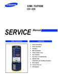
1
SAMSUNG Anycall
SPH-A880
CONTENTS
SAMSUNG Anycall
1.
General Introduction
2.
Specification
3.
Installation
4.
NAM Programming
5.
Circuit Description
6.
Test Procedure
7.
Troubleshooting
8.
Exploded Views and Parts List
9.
Block Diagram
10.
Electrical Parts List
11.
PCB Diagrams
ⓒ Samsung Electronics Co.,Ltd. May. 2005
Printed in Korea.
This Service Manual is a property of Samsung Electronics Co.,Ltd.
Any unauthorized use of Manual can be punished under applicable
International and/or domestic law.
Code No.: GH68-07420A
BASIC.
1. General Introduction
SPH-A880 DBTM(Dual Band Tri Mode) phone functions as analog phone working in AMPS(Advanced
Mobile Phone Service) mode and digital phone working in PCS(Personal Communication Service),
CDMA(Code Division Multiple Access) and GPS modes.
The following standards and minimum performance standards shall be met or exceeded by each
subscriber unit.
Air Interface
TIA/EIA IS-2000 Rel. 0 : Mobile Station-Base Station Compatibility Standard for Dual Mode Spread
Spectrum Systems.
TIA/EIA IS-2000 Rel. 0, Addendum 1 : First Addendum to Mobile Station-Base Station Compatibility
Standard for Dual Mode Spread Spectrum Systems.
TIA/EIA IS-2000 Rel. 0, Addendum 2 : Second Addendum to Mobile Station-Base Station
Compatibility Standard for Dual Mode Spread Spectrum Systems.
TIA/EIA IS-98-D : Recommended Minimum Performance Standards for Dual-Mode Spread Spectrum
Mobile Stations.
TIA/EIA/IS-127 : Enhanced Variable Rate Codec, Speech Service Option 3 for Wideband Spread PCS
Digital Systems.
TIA/EIA/IS-127-2 : Enhanced Variable Rate Codec, Speech Service Option 3 for Wideband Spread
Spectrum Digital Systems - Addendum 2.
TIA/EIA/IS-733-1 : High Rate Speech Service Option 17 for Wideband Spread Spectrum
Communication Systems - Addendum 1 (TTY/TDD Extension).
CDMA Receiver/Transmitter Specifications and Requirements
The Subscriber Unit shall comply with ANSI J-STD-008 and meet or exceed TIA/EIA IS-98D.
The Subscriber Unit shall comply with Personal Station Class II.
Analog Receiver/Transmitter Specifications and Requirements
The Subscriber Unit shall comply with TIA/EIA IS-95B and meet or exceed TIA/EIA IS-95.
The Subscriber Unit shall comply with Mobile Station Power Class III.
1-1
SAMSUNG Proprietary-Contents may change without notice
This Document can not be used without Samsung's authorization
General Introduction
1-2
SAMSUNG Proprietary-Contents may change without notice
This Document can not be used without Samsung's authorization
2. Specification
2-1. General
ITEM
US PCS
Tx Freq. range
1850 ~ 1910MHz
824.04 ~ 848.97MHz 824.04 ~ 848.97MHz
-
Rx Freq. range
1930 ~ 1990MHz
869.04 ~ 893.97MHz 869.04 ~ 893.97MHz
1575.42MHz
Channel Bandwidth
1.23MHz
1.23MHz
30KHz
2MHz
Channel Spacing
50KHz
30KHz
30KHz
Not Used
Number of Channel
1200
832
832
1
Duplex Separation
80MHz
45MHz
45MHz
-
Type of Emission
1M25F9W
1M25F9W
40K0F8W,40K0F1D
-
50Ω
50Ω
50Ω
50Ω
Tx Local Frequency
FTx * 0.7999
FTx * 1.6666
FTx * 1.6666
-
Rx Local Frequency
FRx * 0.8888
FRx * 2
FRx * 2
FRx * 2
TCXO Frequency
19.2MHz
19.2MHz
19.2MHz
19.2MHz
Freq. Stability
(FRX-80MHz)±150Hz
(FRX-45MHz)±300Hz
±2.5ppm
-
-30℃ ~ +60℃
-30℃ ~ +60℃
-30℃ ~ +60℃
-30℃ ~ +60℃
In/Output
Impedance
Operating
Temperature
Supply Voltage
Size and Weight
CDMA
AMPS
3.8 ~ 4.2V
STD : 40.6 * 63.4 * 3.85 mm, 25.2g, 900 mA/H
EXT : 40.9 * 65.7 * 9.24 mm, 37.7g, 1100 mA/H
2-1
SAMSUNG Proprietary-Contents may change without notice
This Document can not be used without Samsung's authorization
GPS
Specification
2-1-1. PCS CDMA(1900MHz)
A. Transmitter
Waveform Quality : 0.944 or more
Open Loop Power Control Range
. -25dBm
: -60.5dBm ~ -41.5dBm
. -65dBm
: -20.5dBm ~ +1.5dBm
. -104dBm
: +15.0dBm ~ +30dBm
Minimum Tx Power Control : below -50dBm
Closed Loop Power Control Range : ±24dB
Maximum RF Output Power : 25dBm
Occupied Bandwidth : 1.23MHz
Conducted Spurious Emission @1.25 MHz: -42dBc/30kHz
B. Receiver
Rx Sensitivity and Dynamic Range :-104dBm, FER=0.5% or less
-25dBm, FER=0.5% or less
Conducted Spurious Emission
. 1930 ~ 1990MHz : < -81dBm
. 1850 ~ 1910MHz : < -61dBm
. All Other Frequencies : < -47dBm
Single Tone Desensitization : lower than 1 %
Rx Power = -101dBm
Tone Power = -30dBm
Tone Offset from Carrier = ± 1.25 MHz
Intermodulation Spurious Response Attenuation : lower than 1 %
Rx Power = -101dBm
Tone Power 1 = -43dBm
Tone Power 2 = -43dBm
Tone 1 Offset from Carrier = ± 1.25 MHz
Tone 2 Offset from Carrier = ± 2.05 MHz
2-2
SAMSUNG Proprietary-Contents may change without notice
This Document can not be used without Samsung's authorization
Specification
2-1-2. CDMA(800MHz)
A. Transmitter
Waveform Quality : 0.944 or more
Open Loop Power Control Range
. -25dBm
: -57.5dBm ~ -38.5dBm
. -65dBm
: -17.5dBm ~ +1.5dBm
. -104dBm
: +18.0dBm ~ +30dBm
Minimum Tx Power Control : below -50dBm
Closed Loop Power Control Range : ±24dB
Maximum RF Output Power : 25dBm
Occupied Bandwidth : 1.23MHz
Conducted Spurious Emission @ 0.9 MHz: -42dBc/30kHz
@ 1.25 MHz: -54dBc/30kHz
B. Receiver
Rx Sensitivity and Dynamic Range :-104dBm, FER=0.5% or less
-25dBm, FER=0.5% or less
Conducted Spurious Emission
. 1930 ~ 1990MHz : < -81dBm
. 1850 ~ 1910MHz : < -61dBm
. All Other Frequencies : < -47dBm
Single Tone Desensitization : lower than 1 %
Rx Power = -101dBm
Tone Power = -30dBm
Tone Offset from Carrier = ± 0.9 MHz
2-3
SAMSUNG Proprietary-Contents may change without notice
This Document can not be used without Samsung's authorization
Specification
Intermodulation Spurious Response Attenuation : lower than 1 %
Rx Power = -101dBm
Tone Power 1 = -43dBm
Tone Power 2 = -43dBm
Tone 1 Offset from Carrier = ± 0.9 MHz
Tone 2 Offset from Carrier = ± 1.7 MHz
2-1-3. AMPS
A. Transmitter
RF Output Power : 26 dBm
Carrier ON/OFF Conditions
"ON" Condition : within ±3dB of specification output(in 2 ms)
"OFF" Condition : below -60dBm(in 2ms)
Compressor
Compression Rate : 2 : 1
Attack Time
: 3 ms
Recovery Time
: 13.5 ms
Reference Input
: input power level for producing a nominal ±2.9kHz
: peak frequency deviation of transmitted carrier
: 6dB/OCT within 0.3 ~ 3 kHz
Preamphasis
Maximum Frequency Deviation
Modulation Deviation Limiting : ±12 kHz
Supervisory Audio Tone
: ±2 kHz(±10%)
Signaling Tone
: ±8 kHz(±10%)
Wideband Data
: ±8 kHz(±10%)
Post Deviation Limiter Filter
3.0 ~ 5.9 kHz
: above 40 LOG(F/3000)dB
5.9 ~ 6.1 kHz
: above 35dB
6.1 ~ 15 kHz
: above 40 LOG(F/3000)dB
Over
: above 28 dB
15 kHz
2-4
SAMSUNG Proprietary-Contents may change without notice
This Document can not be used without Samsung's authorization
Specification
Spectrum Noise Suppression
- For all modulation
fo +20 kHz ~
fo + 45 kHz
: above 26dB
- For modulation by voice and SAT
fo + 45 kHz
: above 63dB+10LOG(PY)dB
- For modulation by WBD(without SAT) and ST(with SAT)
fo +45 kHz ~
fo + 60 kHz
: above 45 dB
fo +60 kHz ~
fo + 90 kHz
: above 65 dB
fo +90 kHz ~ 2 fo
: above 63 dB + 10 LOG(PY) dB
(where fo = carrier frequency, PY=mean output power in watts)
Harmonic and conducted Spurious Emissions : below 43 + 10 LOG(PY) dB
B. Receiver
: -6dB/OCT within 0.3 ~ 3 kHz
De-emphasis
Expandor
Expandor Rate
: 1 : 2
Attack time
: within 3 ms
Recovery Time
: within 13.5 ms
Reference input
: output power level to a 1000Hz tone from a carrier within ±2.9 kHz
peak frequency deviation
Sensitivity
: 12 dB SINAD/-116dBm
Intermodulation Spurious Response Attenuation : above 65dB
RSSI Range : above 60dB
Protection Against Spurious Response Interference : above 60dB
In Band Conducted Spurious Emission
Transmit Band : below
-60 dBm
Receive Band : below
-80 dBm
Out of Band Conducted Spurious Emissions : below -47dBm
2-5
SAMSUNG Proprietary-Contents may change without notice
This Document can not be used without Samsung's authorization
Specification
Radiated Spurious Emission
Frequency Range
: Maximum Allowable EIRP
25 ~ 70MHz
: -45dBm
70 ~ 130MHz
: -41dBm
130 ~ 174 MHz
: -41 ~ -32dBm
174 ~ 260 MHz
: -32 dBm
260 ~ 470 MHz
: -32 ~ -26 dBm
470 ~ 1G MHz
: -21 dBm
2-1-4. GPS
- Location Accuracy
For 67% of calls
:
less than 50 meter
For 95% of calls
:
less than 150 meter
2-6
SAMSUNG Proprietary-Contents may change without notice
This Document can not be used without Samsung's authorization
3. Installation
3-1. Installing and Removing the Battery
To install
To remove
1. Insert the battery into the opening on the back
1. Make sure the power is off.
of the phone.
2. Push the battery release latch up completely.
2. Make sure the plastic tabs on the back are
inserted into the matching slots in the phone.
3. Pull and lift the battery away from the phone.
3. Press down until the latchsnaps into place.
3-2 For Desk Top Use
1. Choose a proper location to install the charger
3. To charger the battery pack, insert the pack into
for desk top use.
the solt of the charger. The lamp on the front
panel of the charger lights up red.
2. Plug the power cord of the charger into an
appropriate wall socket. When the power is
connected correctly, the lamps turn on briefly.
Specifications using Battery Charger
Standard Battery
Battery Type
(Li-ion, 900mAh)
Charging Time
2 hours
SEC-Code
GH43-01821A
3-1
SAMSUNG Proprietary-Contents may change without notice
This Document can not be used without Samsung's authorization
Installation
3-2
SAMSUNG Proprietary-Contents may change without notice
This Document can not be used without Samsung's authorization
4. NAM Programming
NAM program can be changed as following table:
Notes:
- In the NAM program mode, each item show you the currently stored data. you can modify the data
by entering a new data.
- You can move to next window by pressing "OK" key.
- When you press a wrong number, press "BACK" key to delete the last number or press and hold
"BACK " key to delete all number
- You can move to menu screen by pressing "MENU" key.
- You can change some selection option keys by pressing "Left" or "Right" navigation.
4-1. Single NAM
4-1-1. General Setup
LCD Display
Key in
#,#
Enter
??????,#
222222,#
Funtion
Enter the NAM Mode
Enter random 6-digit code (MSL) and #
222222 is a default value.
SVC Menu
1: View
2: Edit
1
View Phone Number and MSID
3: Done
Phone Number
1234567890
MSID
1234567890
Right key or Down
key
MENU or BACK
Phone number is displayed
Mobile ID is displayed
SVC Menu
1: View
2: Edit
2
Choose 'Edit' to change Phone Number and MSID
3: Done
Phone Number
1234567890
- Phone number setup
OK
- To change phone number, enter phone #
- Store it
- Mobile ID setup
MSID
1234567890
OK
- To change phone number, enter phone #
- Store it
SVC Menu
1: View
2: Edit
3
Choose 'Done' to exit the NAM mode
3: Done
4-1
SAMSUNG Proprietary-Contents may change without notice
This Document can not be used without Samsung's authorization
NAM Programming
4-1-2. NAM Mode Display
LCD Display
Key in
Funtion
#,#,3,2,8,2,#
Enter the Data Program screen
5
Display the 3G Data program.
3G Data Prog
1. User Name
2: Browser
3: IOTA Prog.
4: Camera URL
5: Advanced
6: Multimedia
Enter Service Code
??????
222222
Enter random 6-digit code (MSL) - 222222 is a default value
Advanced
1: View
1
Choose "VIEW" to dispaly the Advanced NAM Information
2: Edit
ESN
Right key or Down
B0000000
key
Right key or Down
CERT
key
P_REV
Right key or Down
6
VOCODER SVCOPT
EVRC
SCM
key
Right key or Down
key
Right key or Down
01101010
Lock Code
key
Right key or Down
0016
Slot Mode
key
Right key or Down
YES
Slot Index
key
Right key or Down
2
HOME SID
key
Right key or Down
4139
HOME NID
key
Right key or Down
65535
MCC
key
Right key or Down
310
MNC
key
Right key or Down
00
ACCOLC
key
Right key or Down
6
key
Electronic Serial Number of the phone is displayed
Java security - Dormant Certificate Wakeup(On), and
Sleep(off) status is displayed
Common Air Interface version is displayed
13K or EVRC
Station Class Mark displays the power class,
transmission, slotted class, dual mode.
Lock code, current status is displayed
Slot mode. 'Yes' indicates the slot mode.
Slot mode index. The high number means longer
sleeping time
SID written in the list,current status is displayed.
NID written in the list,current status is displayed.
ImsI Mobile Country Code, current code is displayed.
ImsI Mobile Network Code, current code is displayed.
CDMA Access Overload Class, current status is displayed
4-2
SAMSUNG Proprietary-Contents may change without notice
This Document can not be used without Samsung's authorization
NAM Programming
NAM CDMA
Home Sys Reg
Right key or Down
key
Yes
NAM CDMA
Right key or Down
FSID Reg
key
Yes
CDMA Home system ID, current status is displayed
CDMA foreign SID, current status is displayed.
NAM CDMA
FNID Reg
MENU or BACK
CDMA foreign NID,current status is displayed.
Yes
4-1-3. NAM Mode Setup
LCD Display
Key in
#,#,3,2,8,2,#
Funtion
Enter the Data Program screen ('##DATA')
3G Data Prog
1. User Name
2: Browser
3: IOTA Prog.
5
Display the 3G dara program.
4: Camera URL
5: Advanced
6: Multimedia
Enter Service Code
??????
222222
Enter random 6-digit code (MSL)
- 222222 is a default
value
Advanced
1: View
2
Choose "EDIT" to change the Advanced NAM information
2: Edit
ESN
Right key or Down
B0000000
key
Right key or Down
CERT
key
P_REV
Right key or Down
6
VOCODER SVC OPT
EVRC
SCM
key
Right key or Down
key
Right key or Down
01101010
Lock Code
0016
Slot Mode
key
4-digit Code
OK
Left or Right key
YES
OK
Electronic Serial Number of the phone is displayed
Java security - Dormant Certificate Wakeup(On), and
Sleep(off)
Common Air Interface version is displayed
Origination Service Option is displayed
- Change Service Option
- Store it
Station Class Mark displays the power class,
transmission, slotted class, dual mode.
Lock code, current status is displayed
- To change Lock Code, enter a new code
- Store it
Slot mode. 'Yes' indicates the slot mode.
- Change status
- Store it
4-3
SAMSUNG Proprietary-Contents may change without notice
This Document can not be used without Samsung's authorization
NAM Programming
Slot mode index. The high number means longer sleeping
Slot Index
0 ~ 7
2
OK
time
- To change Slot Index, enter new one
- Store it
HOME SID
4139
HOME NID
65535
MCC
number
OK
number
OK
number
310
MNC
OK
number
00
ACCOLC
OK
class number
6
NAM CDMA
Home Sys Reg
Yes
NAM CDMA
FSID Reg
Yes
NAM CDMA
FNID Reg
Yes
OK
Left or Right key
OK
Left or Right key
OK
Left or Right key
OK
SID written in the list,current status is displayed.
- Enter new one to change code
- Store it
NID written in the list,current status is displayed.
- Enter new one to change code
- Store it
ImsI Mobile Country Code, current code is displayed.
- Enter new one to change code
- Store it
ImsI Mobile Network Code, current code is displayed.
- Enter new one to change code
- Store it
CDMA Access Overload Class, current status is displayed
- Enter new one to change code
- Store it
CDMA Home system ID, current status is displayed
- Change status
- Store it
CDMA foreign SID, current status is displayed.
- Change status
- Store it
CDMA foreign NID,current status is displayed.
- Change status
- Store it
4-4
SAMSUNG Proprietary-Contents may change without notice
This Document can not be used without Samsung's authorization
5. Circuit Description
5-1. Logic Part
5-1-1. Power Supply
Press "END/ⓛ" key to turn on the phone and then the S3.6 and ON_SW signals will be
connected. This turn on inner regulator(V_MSMC, V_PA, VPD) of U200(MAX1526) and
release them from the shut down state to output regulated 1.83V(V_MSMC), 2.6V(V_MSMA) and
2.6V(VPD).
The S3.6 applied to ON_SW will activate U200(MAX1526). This will allow MSM(U101) to send out
PS_HOLD(logic HIGH) to continue turning on inner regulator(V_MSMC, V_PA, VPD)
even
after the END/ⓛ key is released.
The other regulators will be controlled ON/OFF state by I2C-compatible 2 wire serial interface.
The regulated voltage VPD is used in the digital part of MSM and Memory(U102) Part.
The regulated voltage VPA is used in the analog part of MSM.
The regulated voltage V_MSMC is used in the core part of MSM/Memory.
The regulated voltage V_RFTX is used in the TX RF part of S1M8690X.
The regulated voltage V_RFRX is used in the Rx RF part.
The regulated voltage V_TCXO is used in the VCO part and TCXO part.
The regulated voltage V_SYNTH is used in the RFT circuit of PLL part.
5-1-2. Logic
The logic part consists of internal CPU of MSM, NAND and SDRAM. The MSM receives TCXO
clock signal, and controls the phone during the PCS, CDMA and the FM mode.
The major components are as follows:
- CPU
: ARM926EJ-S CPU core
- MCP(Multi-Chip Package)
? NAND and SDRAM : U102(K5D5657DCM-F015)
- 256Mbit(32Mx8) NAND Flash / 256Mbit(4Mx16x4 Banks) Mobile SDRAM
5-1
SAMSUNG Proprietary-Contents may change without notice
This Document can not be used without Samsung's authorization
Circuit Description
CPU(U101:MSM6100-341CSP)
ARM 9 CMOS type 32-bit ARM/16-bit THUMB microprocessor is used for the main processing.
The CPU controls all the circuitry. The MSM6100 derives all of its internal clock sources from
three clock input TCXO(19.2MHz), SLEEP_XTAL(32.768KHz,in Sleep Mode), 48XTAL(48MHz, If
used USB).
32.768KHz is used for sleep mode. This is equipped with the ARM 9 CPU core,
CDMA and DFM block, vocoder, general purpose interface and other interfaces.
It is one of the most important components of the CDMA cellular phone.
MCP : NAND and SDRAM (U102 : K5D5657DCM-F015)
Memories consist of 256Mbit NAND Flash Memory and 256Mbit synchronous high data rate
Dynamic RAM. In 256Mbit NAND Flash, a (512+16)Byte page program can be typically
achieved within 200us and and (16K+512)Byte block erase can be typically achieved within 2ms.
In serial read operation, a byte can be read by 50ns. IO pins serve as the ports for address
and data input/output as well as command inputs. In 256Mbit SDRAM, Synchronous design
make a device controlled precisely with the use of system clock and I/O transactions are
possible on every clock cycle.
Keypad
For key recognition, key matrix is setup using SCAN(1:7)
and KEYSENSE(0:3)
of input/output ports of MSM. 16 backlight LEDs and back-light circuitry are
included in the keypad for easy operation in the dark.
LCD Module
The Subscriber Units should have a 65K color TFT LCD of Main(176x220 pixels) and
Sub(96x96 pixels). The display shall be capable of presenting animation.
5-1-3. Baseband
Mobile System Modem(MSM)
The MCU equipped with the ARM 9 CPU core is an important component of the CDMA
cellular phone. The MSM comes in a 341-Ball CSP Package.
5-2
SAMSUNG Proprietary-Contents may change without notice
This Document can not be used without Samsung's authorization
Circuit Description
MICROPROCESSOR INTERFACE
The interface circuitry consists of reset circuit, address bus(A0-A14), data bus(D(0:15), D2(0:15)),
and memory controls ( DRAM_RAS, RAM_CS2_N, NAND_CLE, NAND_ALE, ROM_WP ).
CODEC
The MSM6100(U101) integrates an audio voiceband CODEC into the Mobile
Station Modem. The integrated CODEC contains all of the required conversion
and amplification stages for the audio front end.
HPADC
The MSM6100(U101) has an on-chip 8bit analog-to-degital(HPADC) which is
intended to digitalize DC signal corresponding to analog parameters such as
Battery voltage, Temperature, and RF power levels.
Clock
CPU clock
: 19.2MHz. This clock signal from the TCXO
Sleep clock
: 32.768KHz. This clock signal is used for sleep.
TCXO/N
: 19.2/N MHz. This clock source is used by various blocks of the MSM6100
device, such as the ARM926EJ-S, ringer, UARTs, general-purpose PDMs and
the Digital FM circuit. TCXO can be used as a vocoder clock source for EVRC
support.
USB clock : 48MHz. This clock signal is used to drive the USB interface on the MSM6100.
RFR6000, SIM8690X and MSM INTERFACE
A. CDMA, FM Data Interface
- I_OUT, I_OUT_N and Q_OUT, Q_OUT_N(U402) :
Differential output for I and Q component used during CDMA and FM mode.
- RX_IDATA (U401 pins 30-31) and RX_QDATA(U401 pins 33-34) :
RX data bus used during CDMA.
5-3
SAMSUNG Proprietary-Contents may change without notice
This Document can not be used without Samsung's authorization
Circuit Description
B. Clock
- TCXO : 19.2 MHz is used in CDMA mode.
C. RF Interface
- TX : TX_AGC_ADJ(U101 pin R24) port is used to control the TX power,
PA_ON_PCS(U101 pin C23) signal used to control the PCS power amplifier and
PA_ON_CELL(U101 pin F24) signal used to control the CDMA power amplifier.
5-1-4. Audio Part
The MSM6100 integrates an audio voiceband Codec into Mobile Station Modem.
The integrated Codec contains of all the required conversion and amplification stages for the
audio front end. The Codec operates as a 13bit linear Codec with the transmit(TX) and
receive(RX) filters designed to meet ITU-TG.712 requirement. The CODEC contains the
software controller amplifier for both the receiving and transmitting sections. Also, the
vocoding schemes used will be 13kbps QCELP and 8Kbps EVRC. The QCELP vocoder is
based in the MSM internally.
Tx Audio Path
The voice signal from the microphone is inputted to the internal CODEC. The voice signal
is then amplified by the internal amplifier and is converted to PCM data to be outputted to
the MSM as 13bit data. This data is then processed by the MSM(U101)'s internal.
RX Audio Path
The PCM data from the MSM(U101)'s internal is inputted to the internal CODEC and the
data will be decoded by the internal DAC and audio levels are adjusted by the amplifier.
The final audio is then sent to the audio receiver.
5-4
SAMSUNG Proprietary-Contents may change without notice
This Document can not be used without Samsung's authorization
Circuit Description
Buzzer Driving Circuitry
A speaker generates alert tone and melody. When the MSM(U101) receives the data, it's
internal CMX generates alert tone and melody. Ringer signal generated in MSM6100 is
intended to drive a speaker.
Key Tone Generator
The CODEC data out from the MSM6100 is converted to DTMF signal by TONE generator of
internal CODEC, is then amplified by the internal audio amplifier to be sent to the speaker
unit.
Digital FM Block
The digital FM processor is included in the MSM6100.
FM Transmit Processor
A. Pre-Emphasis Circuit
This part features +6dB/oct to reduce signal loss and noise in Tx path.
B. Compressor
The compressor features 2:1 level compressor to reduce signal loss and noise in Tx
path. The zero crossing level of the compressor is ±2.9 kHz/dev, attack time is 3ms,
and release time is 13.5ms.
C. Limiter
The limiter performs to cut ±0.53 Vp-p or higher audio signal level so that the FM
frequency deviation is not over ±12kHz/dev. The function is used to avoid confusion
over phone line LPF is used to reduce a specific high frequency of limited signal.
5-5
SAMSUNG Proprietary-Contents may change without notice
This Document can not be used without Samsung's authorization
Circuit Description
FM Receiver Audio Path
A. De-Emphasis Circuit
This part features -6dB/oct filter to reduce signal loss and noise in Rx path.
B. Expandor
The expandor features 1:2 level increaser to reduce signal loss and noise in Rx path.
The zero crossing level of the expander is ±2.9kHz/dev, attack time is 3ms, and
release time is 13.5ms.
5-1-5. TX WBD, ST and SAT
The WBD and ST are generated by the MSM6100 but the SAT is generated by the S1M8690X.
The modulation level of TX WBD and ST is ±8kHz/dev and SAT is ±2kHz/dev.
5-2. RF Part
5-2-1. Transmitter
FOR CDMA PCS(1900MHz)
Antenna
Antenna sends signal to the base station and receives the signal from the base station.
It is a tri-band Antenna and covers PCS band, CDMA band, AMPS band and GPS band.
RF Switch
It(U400:TQP4M3018) is used to switch the PCS/AMPS path and the GPS path,
The RF signal pass through PCS/AMPS path when GPS_MODE is low.
Duplexer & Power AMP module
Duplexer(F401:AFEM-7731) allows to transmit only the signals within acceptable Tx
frequency range (1880 ± 30 MHz) through the antenna.
Power amplifier module(F401:AFEM-7731) amplifiers signal to be sent to the base station
through the antenna.
5-6
SAMSUNG Proprietary-Contents may change without notice
This Document can not be used without Samsung's authorization
Circuit Description
RF Band Pass Filter(Tx RF SAW Filter)
The RF BPF(F400:ACPF-7002-TR1) pass only specific frequency(1880±30MHz) to send it to
power amp(U401:AFEM-7731).
Driver Amp
The driver amp(U402 ; included in S1M8690X) allows the signal to be inputted to the
power amp(U401) as a specified level.
Up-converter(Mixer)
The up-converter(U402 ; also included in S1M8690X) receives the local signal
FTx * 0.7999
and signal controlled by TX AGC amp(in S1M8690X) to generate Tx RF signal 1880±30MHz
which signal comes out from the mixer output by adding
FTx * 0.7999 local signal.
Automatic Gain Control Amp
The TX IF AGC amp (in S1M8690X) controls gain of AGC to deliver power level needed at
driver amp. Its control voltage varies from 0.2V to 2.5V.
For CDMA (800MHz) and AMPS
Antenna
Antenna sends signal to the base station and receives the signal from the base station.
It is a tri-band Antenna and covers PCS band, CDMA band, AMPS band and GPS band.
RF Switch
It(U400:TQP4M3018) is used to switch the PCS/AMPS path and the GPS path,
The RF signal pass through PCS/AMPS path when GPS_MODE is low.
Duplexer
Duplexer(F402:SFX836LC601) allows Rx frequency range(881.49 ±12.5 MHz) and Tx frequency
range
5-7
SAMSUNG Proprietary-Contents may change without notice
This Document can not be used without Samsung's authorization
Circuit Description
(836.49 ±12.5 MHz) from the antenna to pass through LNA. It also matches LNA input in
receiving part and PAM(U401:ACPM-7813) output in transmitter part with the antenna.
Power Amp
Power amplifier module(U401:ACPM-7813) amplifiers signal to be sent to the base station
through the antenna.
RF Band Pass Filter(Tx RF SAW Filter)
The RF BPF(F403:H836NF) pass only specific frequency(836.49 ±12.5MHz) to send it to power
amp(U504:ACPM-7813-DC1).
Driver Amp
The driver amp(U402 ; included in S1M8690X) allows the signal to be inputted to the
power amp(U401) as a specified level.
Up-Converter(Mixer)
The up-converter(U402 ; included in S1M8690X) receives the local signal
FTx * 1.6666
and the signal controlled by TX AGC amp(in S1M8690X) to generate Tx RF signal
836.49±12.5MHz signal comes out from the mixer output by adding
FTx * 1.6666 local signal.
Automatic Gain Control Amp
The TX IF AGC amp in S1M8690X controls gain of AGC to deliver power level to be needed
at Driver amp. Its control voltage varies from 0.2V to 2.5V.
5-2-2. Receiver
FOR CDMA PCS(1900MHz)
Low Noise Amplifier(LNA)
The low noise amplifier(It is included in FC7510 : U300) amplifies a weak signal received from
5-8
SAMSUNG Proprietary-Contents may change without notice
This Document can not be used without Samsung's authorization
Circuit Description
the base station to obtain the optimum signal level.
RF Band Pass Filter(Rx RF SAW Filter)
The RF BPF(F301:FAR-F6EB-1G9600-B2BKH) passes only a specific frequency(1960±30 MHz)
from the signal received from the mobile station. The bandwidth is 60 MHz.
Down Converter(MIXER)
The local signal is applied to the down converter in RFR6000 : U301
This component converts the RF signal from the LNA to baseband signal.
The baseband signal is made by subtracting local signal(FRx
* 0.8888)
from RF signal(1960±30MHz).
For CDMA(800MHz) and AMPS
Low Noise Amplifier(LNA)
The low noise amplifier(It is included FC7510 : U300) amplifies a weak signal received from
the base station to obtain the optimum signal level.
RF Band Pass Filter(Rx RF SAW Filter)
The RF BPF in (F300:H881YS) passes only a specific frequency(881.49±12.5 MHz) from the
signal received from the mobile station. The bandwidth is 25 MHz.
Down Converter(MIXER)
The first local signal is applied to this down converter in RFR6000 : U301. The down converter
converts the RF signal from LNA into baseband signal. The baseband signal is made by
subtracting local signal (FRx
* 2) from RF signal(881.49±12.5 MHz).
5-9
SAMSUNG Proprietary-Contents may change without notice
This Document can not be used without Samsung's authorization
Circuit Description
5-2-3. GPS(1575.42MHz)
Antenna
Antenna receives signal from GPS satellites.
It is a tri-band Antenna and covers PCS band, CDMA band, AMPS band and GPS band.
RF Switch
It(U400:TQP4M3018) is used to switch the PCS path and AMPS/CDMA path and the GPS
path.
The RF signal pass through PCS path when PCS_MODE is high(3.0V).
pass through AMPS/CDMA path when CELL_MODE is high(3.0V).
The RF signal
The RF signal pass through
GPS path when GPS_MODE is high(3.0V).
RF Band Pass Filter(Rx RF SAW Filter)
The RF BPF(F302:B9000) passes only a specific frequency(1575.42±2 MHz) from the signal
received from the satellite.
The bandwidth is 2 MHz.
Down Converter(MIXER)
The first local signal is applied to this down converter in RFR6000 : U301). The down converter
converts the RF signal from LNA into baseband analog signal. The baseband analog signal is
made by subtracting local signal from the RF signal(1575.42MHz).
5-2-4. PLL Block
Frequency Synthesizer Circuit
The PLL(Phased Locked Loop) block consists of VC-TCXO(OSC301:TOH1920DPH4KRA),
PLL in S1M8690X and VCO(OSC300:MQL300A1G75).
Input reference frequency is generated at VC-TCXO and the RF local signal is generated at
VCO. PLL compares the two signals and generates the desired signal with a preprogrammed
counter which controls voltage.
5-10
SAMSUNG Proprietary-Contents may change without notice
This Document can not be used without Samsung's authorization
Circuit Description
VC-TCXO
The VC-TCXO (OSC301) is a reference source of the frequency synthesizer. It provides 19.2MHz
reference frequency to PLL-IC. It is a voltage controlled temperature compensated crystal
oscillator having 19.2MHz ±2.5ppm frequency stability over all useful temperature range.
A correct frequency tuning is made by the control voltage.
Voltage Controlled Oscillator
The VCO(OSC300) generates the signal having center frequency 1715 ~ 1788MHz frequency
range with the voltage control.
The PLL in S1M8690X controls this signal.
5-11
SAMSUNG Proprietary-Contents may change without notice
This Document can not be used without Samsung's authorization
Circuit Description
5-3. Test Command Table
To change the phone from normal mode to test mode, you should enter the following keys. :
Press [4 7 * 8 6 9 # 1 2 3 5]
1
T_SUSPEND_I
Enter to TestMode
2
T_RESTART_I
Escape from TestMode
3
T_SAVE_VAL_I
Save values to EEPROM
4
T_WRITE_NV_I
Write the EEPROM item
5
T_VOLUME_UP_I
Electric Volume Up
6
T_VOLUME_DOWN_I
Electric Volume Down
11
T_CARRIERON_I
Turn on the carrier
12
T_CARRIEROFF_I
Turn off the carrier
13
T_LOADSYN_I
Load the synthesizer for locking
14
T_CDATA_I
15
T_TRK_LO_ADJ_I
16
T_RX_DVGA_OFFSET_I
Adjust Rx DVGA gain offset
17
T_LNA_OFFSET_I
Adjust Rx LNA gain offset
19
T_TX_AGC_ADJ_I
Set Tx AGC code
20
T_TX_CH_FLAT_ADJ_I
21
T_SIO_MODE_I
Change SIO mode
22
T_TEST_SYS_I
Change band & channel
23
T_MRU2_TABLE_I
Reset MRU
24
T_NAI_SET_I
Factory Default NAI(Temporary)
25
T_SET_BTF_I
Set PCS BTF
27
T_TX_CH_FLAT_MAX_I
Adjust Tx channel MAX PWR flatness
28
T_TX_CH_FLAT_MIN_I
Adjust Tx channel MIN PWR flatness
29
T_FM_RSSI_RAW_MIN_I
Set FM raw rssi min
30
T_FM_RSSI_RAW_MAX_I
Set FM raw rssi max
31
T_VERSION_I
Send model/sw ver/hw ver/buyer
32
T_SNDNAM_I
Send NAM Information
33
T_SNDVERSION_I
Send Software Version
34
T_SNDESN_I
Send ESN
35
T_WRT_PLINFO_I
Write Product line information
36
T_RD_PLINFO_I
Read Product line information
37
T_REBUILD_I
Rebuilding EEPROM
38
T_PHONE_RESET_I
UI Features reset
41
T_BACKLIGHT_I
Backlight on / off
42
T_LED_I
LAMP on / off
Send TX Control data continuously
Adjust tracking local
Adjust Tx channel flatness
5-12
SAMSUNG Proprietary-Contents may change without notice
This Document can not be used without Samsung's authorization
Circuit Description
43
T_VIBRATOR_I
Vibrator on / off
44
T_DTMFON_I
Turn on DTMF
45
T_DTMFOFF_I
Turn off DTMF
48
T_CAMERA_FLASH_I
Camera Flash on / off
51
T_BATT_TYPE_I
Check battery type
52
T_READ_BATT_I
Read battery code
53
T_SET_STBY_BATT_I
Adjust Stby batt code
54
T_SET_TALK_BATT_I
Adjust Talk batt code
55
T_THERM_READ_I
Read a thermister
61
T_FM_PWRLEVEL_I
Change AMPS power level
62
T_SET_EXT_AUDIO_I
External audio path on/off
63
T_FM_VCLINE_I
64
T_ALLPATH_I
Tune on the all audio path
65
T_FM_RX_AUDIO_I
Mute/Unmute rx audio
66
T_FM_TX_AUDIO_I
Mute/Unmute tx audio
68
T_FM_ST_I
Turn on/off ST
69
T_FM_SAT_I
Turn on SAT
70
T_FM_COMPAND_I
Turn on compandor
71
T_FM_ST_GAIN_I
Adjust FM ST gain
72
T_FM_SAT_LEVEL_I
Adjust FM SAT level
73
T_FM_FREQ_SGAIN_I
Adjust FM fequency sense gain
74
T_TX_LIMITER_I
Adjust Tx Limiter
75
T_VOC_PCM_LOOP_I
Turn on/off to play a PCM LOOP BACK
78
T_SND_SND_CAL_I
Set voice rx gain
79
T_SND_RING_CAL_I
Set Ring marjin gain
81
T_GPSONE_MODE_I
Set single/continuous mode
82
T_GPSONE_GPS_RF_DELAY_FOR_PCS_I
84
T_GPSONE_ACCURACY_I
85
T_GPSONE_ANT_OFF_DB_I
Set gps antenna offset.
86
T_GPSONE_LO_BIAS_UPDATE_CNT_I
Set gps local bias update counter
87
T_GPSONE_GPS_LO_CAL_I
Set gps local calibration value.
88
T_GPSONE_GPS_RF_LOSS_I
Set gps rf loss
89
T_GPSONE_GPS_RF_DELAY_I
Set gps rf delay
90
T_GPSONE_CDMA_RF_DELAY_I
Set cdma rf delay
91
T_GET_RX_BASIS_I
get rx_basis_offset (via hfk command only)
92
T_SET_RX_BASIS_I
set rx_basis_offset
93
T_GET_TEMP_VS_FREQ_I
get temp_vs_freqoffset (via hfk command only)
94
T_SET_TEMP_VS_FREQ_I
set temp_vs_freq_offset
Enetr FM voice state
GPS rf delay in pcs mode
GPS ACCURACY
5-13
SAMSUNG Proprietary-Contents may change without notice
This Document can not be used without Samsung's authorization
Circuit Description
95
T_CDMA_RAS_PER_FAC_I
set cdma ras percent factor
96
T_PCS_RAS_PER_FAC_I
set pcs ras percent factor
97
T_CDMA_CH_PER_FAC_I
set cdma channel percent factor
98
T_PCS_CH_PER_FAC_I
set pcs channel percent factor
99
100
T_READ_ADJUST_VAL_I
Read rf calibration value.
101
102
103
T_GET_TEMP_VS_PWR_I
get temp_vs_pwr_offset (via hfk command only)
104
T_SET_TEMP_VS_PWR_I
set temp_vs_pwroffset
105
T_FM_CH_PER_FAC_I
set amps_ percent factor
106
107
108
109
110
T_TXRAS_ADJ_I
111
T_TEST_SET_LNA_RANGE_I
112
T_SET_LNA_RISE_FALL_I
113
T_SET_ADJUST_VAL_I
set Dvga,LNA offset setting
114
T_SET_PDM_VALUE_I
set pdm value
115
T_READ_ADC_PWR_I
116
T_NV_MAJVER_I
117
T_HW_VER_I
118
T_OTKSL_EDIT_I
set lna range
lna rise setting
read ADC_Fwd,ADC_Rev
119
120
T_2ND_TXRAS_ADJ_I
121
T_SET_PA_R1_R0_I
122
T_CENTER_ADJ_I
123
124
125
126
127
T_NV_ENUM_INFO_I
128
T_SET_RDF_PATH_I
129
T_CLEAR_MEMORY_I
Change RDF file path
130
5-14
SAMSUNG Proprietary-Contents may change without notice
This Document can not be used without Samsung's authorization
Circuit Description
131
132
133
139
T_READ_BACKUP_I
read abckup items
140
T_NV_BACKUP_ERASE_I
erase backup items
143
T_VIBRATOR_ON_I
turn vibrator on
144
T_VIBRATOR_OFF_I
turnvibrator off
149
150
T_MAX_I
5-15
SAMSUNG Proprietary-Contents may change without notice
This Document can not be used without Samsung's authorization
Circuit Description
5-16
SAMSUNG Proprietary-Contents may change without notice
This Document can not be used without Samsung's authorization
6. Test Procedure
6-1. List of Equipment
● DC Power Supply
● Test Jig
● Test Cable
● CDMA Mobile Station Test Set
HP8285A, HP8960, CMD-80, etc
● Spectrum Analyzer(include CDMA Test Mode) HP8596E
6-2. Configuration of Test
6-2-1. Hand Set
6-2-2. Hands-Free
6-1
SAMSUNG Proprietary-Contents may change without notice
This Document can not be used without Samsung's authorization
Test Procedure
6-2-3. Test Cable Connection Diagram
TEST INTERFACE BOX
AUTO SELECT
DC POWER INPUT POR T
LEFT: AUDIO IN
RIGHT: AUDIO OFF
CHANGE VOLTAGE LEVEL
BY MODEL (3.8 VDC)
• RED: +
• BLACK: GND
UP: AUTO POWER ON
DOWN: NOT USE
DB25 CONNECTOR
CONNECT TO DB25
CONNECTOR OF
TEST CABLE
T
E
S
T
AUTO
A-IN
RED(+)
BLK(-)
DB9 CONNECTOR
DC3.8V
TO PC
CONNECT TO IBM PC
SERIAL PORT
TEST INTERFACE BOX
P
A
C
K
TO HP
RJ11 CONNECTOR
CONNECT TO HP
SERIAL PORT
TO A-OUT
CONNECT TO
AUDIO OUT PORT OF
TEST EQUIPMENT
(USE BNC CABLE)
TO A-IN
CONNECT TO
AUDIO IN PORT OF
TEST EQUIPMENT
(USE BNC CABLE)
PROBE
NOT USED
TEST CABLE
DB25 CONNECTOR
I/F CONNECTOR
CONNECT TO DB25 CONNECTOR OF
TEST CABLE
CONNECT TO HHP
Items needed to purchase from SAMSUNG
ITEMS
TEST CABLE
TEST INTERFACE
BOX
DM Cable
PARTS#
GH39-00172A
REMARK
*Cable Loss : 1.9 GHz(PCS) 2.1dB, 800 MHz(Cellular) 1.4dB (1.8m)
Including
GH80-00001A
1. Power Cable(Black, Red)
2. 9-pin RS 232 Cable for PC
GH59-00054A
Connection between Phone and PC
6-2
SAMSUNG Proprietary-Contents may change without notice
This Document can not be used without Samsung's authorization
Test Procedure
mode.
6-3. Test Procedure
. If you enter the command [0 1 9] you can
6-3-1. Change the test mode
control the power output level. Following
A. To change the phone from normal mode to test
under bar means AGC code. And you can
mode, you should enter the following keys.
control the power output level using
: Press [4 7 * 8 6 9 # 1 2 3 5]
[TALK]/[END/①] keys.
B. The command [0 0 1] (Suspend) is entered to
ex) [0 1 9 X X X]
start test.
. [#] key means the escape of current command.
: Press [0 0 1]
800 MHz CELLULAR (AMPS)
C. To finish the test mode, you should enter the
command [0 0 2]
A. To select AMPS mode, you should enter the
: Press [0 0 2]
following keys.
1) Press [4 7 * 8 6 9 # 1 2 3 5].
6-3-2. Channel selection and Tx power
output level control
2) Press [0 2 2 1 0 0 0 0] + [OK] + [0 0 2]
1.9 GHz (PCS)
means SYS_B.
ex) [1 0 0 0 0] means SYS_A, and [1 0 0 0 1]
B. You should change the phone from normal
A. To select PCS mode, you should enter the
mode to test mode.
following keys.
: Press [4 7 * 8 6 9 # 1 2 3 5]
1) Press [4 7 * 8 6 9 # 1 2 3 5]
C. You should enter the following keys.
2) Press [0 2 2 3 0 0 0 0] + [OK] + [0 0 2]
: Press [0 1 3 0 3 6 3] + [#] + [0 1 1] + [0 1 9
B. You should change the phone from normal
3 0 0]
mode to test mode
. If you enter the command [0 1 3] you can
: Press [4 7 * 8 6 9 # 1 2 3 5]
select the channel.
C. You should change [0 0 1] (Suspend) is
ex) [0 1 3 X X X X] ; Under bar means channel
entered to start test.
number, and channel number must be 4 digits.
: Press [0 0 1]
. The command [0 1 1] means carrier on.
D. You should enter the following keys.
. If you enter the command [0 1 9] you can
: Press [0 1 3 0 6 0 0] + [#] + [0 1 1] + [0 1 4]
control the power output level. Following under bar
+[0 1 0 1] + [#] + [0 1 9 3 0 0]
means AGC code. And you can control the power
. If you enter the command [0 1 3] you can
output level using [TALK]/[END/① ] keys.
select the channel.
ex) [0 1 9 X X X]
ex) [0 1 3 X X X X] ; Under bar means channel
. [#] key means the escape of current command.
number, and channel number must be 4 digits.
. The command [0 1 1] means carrier on.
. If you enter the command [0 1 4] you can
spread the carrier.
. If you enter the command [0 1 0 X] you can
set PA gain mode, and number must be 0 or 1.
0 means low gain mode, and 1 means high gain
6-3
SAMSUNG Proprietary-Contents may change without notice
This Document can not be used without Samsung's authorization
Test Procedure
800 MHz (CDMA)
A. To select CDMA mode, you should enter the
following keys.
1) Press [4 7 * 8 6 9 # 1 2 3 5]
2) Press [0 2 2 2 0 0 0 0] + [OK] + [0 0 2]
B. You should change the phone from normal
mode to test mode
: Press [4 7 * 8 6 9 # 1 2 3 5]
C. You should change [0 0 1] (Suspend) is
entered to start test.
: Press [0 0 1]
D. You should enter the following keys.
: Press [0 1 3 0 3 6 3] + [#] + [0 1 1] + [0 1 4]
+[0 1 0 1] + [#] +[0 1 9 3 0 0]
. If you enter the command [0 1 3] you can
select the channel.
ex) [0 1 3 X X X X] ; Under bar means channel
number, and channel number must be 4 digits.
. The command [0 1 1] means carrier on.
. If you enter the command [0 1 4] you can
spread the carrier.
. If you enter the command [0 1 0 X] you can
set PA gain mode, and number must be 0 or 1.
0 means low gain mode, and 1 means high gain
mode.
. If you enter the command [0 1 9] you can
control the power output level. Following under bar
means AGC code. And you can control the power
output level using [TALK]/[END/①] keys.
ex) [0 1 9 X X X]
. [#] key means the escape of current command.
6-4
SAMSUNG Proprietary-Contents may change without notice
This Document can not be used without Samsung's authorization
7. Troubleshooting
7-1. Logic Section
7-1-1. No Power
Insert PWR
U200 pin10 =2.6V
No
U200 pin8= 2.6V
Check U200 and its neighboring
circuits.
Yes
L206 = 1.83V
No
Check U200, L200, R210, R212,
C212 and its neighboring circuits
Yes
PWR on
7-1
SAMSUNG Proprietary-Contents may change without notice
This Document can not be used without Samsung's authorization
Troubleshooting
POWER-IC
S3.6
C200
C206
C201
C202
C203
DC_VOLT
C205
D200
C207
VPD_2.6V
VPD_2.6V
U200
R208
REFBP
R211
R214
R205
C210
45
31
32
33
L200
29
28
27
R210
L206
V_MSMC_1.83V
R212
C212
C213
48
10
8
RESETIN_N
VPA_2.6V
VPD_2.6V
13
OUT3 43
RX_EN 7
OUT4
1
OUT5 39
TCXO_EN
47
OUT6 3
_OE
OUT7
SUSPEND
RCV
OUT8 5
VP
OUT9 6
VM
49
GND 50
NC 51
NC
V_RFRX_2.85V
RX_CTRL
11
INV1
12 CO
MP1
15
14 INV2
COMP2
EAR_REF
EAR_DET
EAR_MIC+
SEND_END
16
17
20
21
22
C228
C229
C230 C218
GND
USB_OE_N
USB_SUSPEND
USB_DATA
USB_VPO
USB_VMO
V_TCXO_2.85V
TCXO_CTRL
V_SYNTH_2.85V
V_RFTX
MOTOR_EN_3.1V
V_LED_3.3V
C219 C220 C221 C222 C223 C224
C226 C227
DD+
VTRM
VUSB
HW_RESET
PM_DATA
PM_CLK
36
VL
LX1
37
PGND1
38 VICHG
_AC_OK
FB1
2
LX2
46 _ONO
PGND2
26 PWR_ON
HP_PWR
FB2
41 PW
R_HOLD
_RESET
42
OUT1
25 _HRESET
DA
TA
OUT2
40 CLK
VICHG
TA_DET
ON_DET
ON_SW
HP_PWR
PS_HOLD
C211
BATT
IN1
IN2
IN3
R206
CHG_IN
35 34 30 94
D201
44 23241918
D202
V_BUS
VPULL
D+_IN
D-_IN
C233
7-2
SAMSUNG Proprietary-Contents may change without notice
This Document can not be used without Samsung's authorization
Troubleshooting
7-1-2. LCD Working
Insert Power
Main LCD Back
Check C238,
-light On?
C264 = High?
No
Check CN201 and it's
No
neighboring circuits
Yes
Change LCD
Yes
Check CN201,
OK?
Replace CN201,F200,F201,
F200,F201,F202,
LCD Display
No
F203 and it's
Short=?
F202,F203 and it's
Yes
neighboring circuits
Yes
No
Change LCD
END
7-3
SAMSUNG Proprietary-Contents may change without notice
This Document can not be used without Samsung's authorization
Troubleshooting
F 200
VPD_2.6V
R238
R239
VPD_2.6VS3.6
D2(1)
1 IN
OUT 5
D2(0)
2 IN
OUT 6
D2(2)
3 IN
OUT 7
D2(4)
4
IN
D_L(1)
D_L(0)
D_L(2)
OUT 8
D_L(4)
D2(5)
1 IN
OUT 5
D_L(5)
D2(6)
2 IN
OUT 6
3 IN
OUT 7
GG
R240
9
10
CN201
1
3
5
78
9
LCD_WR_L
LCD_RS_L
MAIN_LCD_CS_L
SENSOR_PWR _ON_L
RESOUT_N
FLASH_MODE
CAM_SCL
CAM_SDA
MCLK
PCLK
11
13
15
17
19
21
23
25
27
29
31
33
35
37
39
41
43
45
47
49
51
53
HREF
VSYN C
CAM_FLAS H_EN
BL_DIM
MOTOR_EN_3.1V
SPK+
SPKLED_R
BL_EN
1
3
5
7
9
11
13
15
17
19
21
23
25
27
29
31
33
35
37
39
41
43
45
47
49
51
53
2
4
6
8
10
12
14
16
18
20
22
24
26
28
30
32
34
36
38
40
42
44
46
48
50
52
54
2
4
6
D_L(0)
D_L(1)
D_L(2)
D_L(3)
D_L(4)
D_L(5)
D_L(6)
D_L(7)
D_L(8)
D_L(9)
D_L(10)
D_L(11)
D_L(12)
D_L(13)
D_L(14)
D_L(15)
10
12
14
16
18
20
22
24
26
28
30
32
34
36
38
40
42
44
46
48
50
52
54
F201
D2(8)
D2(10)
4
IN
91
D_L(8)
D_L(10)
0
D2(11)
1 IN
OUT 5
D2(13)
2 IN
OUT 6
3 IN
OUT 7
D2(14)
D2(7)
4
IN
OUT 8
G
91
C264
C263
C270
C280
C278
C277
C276
C275
C274
C273
C272
C282
C281
C269
G
F202
Y7
Y6
Y5
Y4
Y3
Y2
Y1
Y0
DUAL _REG_EN
C481
C489
OUT 8
G
D_L(6)
G
D_L(11)
D_L(13)
D_L(14)
D_L(7)
0
F203
D2(9)
1 IN
OUT 5
D2(12)
2 IN
OUT 6
3 IN
OUT 7
D2(15)
LCD_RSL
4
IN
9
7-4
SAMSUNG Proprietary-Contents may change without notice
This Document can not be used without Samsung's authorization
OUT 8
GG
10
D_L(9)
D_L(12)
D_L(15)
CD_RS_L
Troubleshooting
7-1-3 Speaker, Receiver and Mic Checking
Insert Power
YES
Check R236,
Speaker is
U453, U454
OK?
NO
Replace U467
NO
signal OK?
YES
YES
Replace speaker
Check R207,
R220, U201 /
Receiver is
OK?
RelpaceU201,
U202 4pin
NO
U202
NO
signal OK?
YES
YES
Replace receiver
NO
Check D206,
MIC is OK?
NO
Check mic path from
D207signal OK?
YES
YES
END
Check Mic FPCB
7-5
SAMSUNG Proprietary-Contents may change without notice
This Document can not be used without Samsung's authorization
U101.
Troubleshooting
AU DIO_AM P
S3.6
U456
VDD
VSS 11
U467
VSS 10
VIP
VOP 9
3
U461
R336
4
5
7
VDD
VDD
6
SPK+
8
S3.6
R207
U464
U454
EN
VSS
INTERNAL _ON
SPKU463
VIM
VSS
EAR_L
R335
U453
13
14
VOM 12
2
C342
15
VDD
16
GND
17
18 NC
19 NC
1
VREF
VDD
C491
VDD
U458
U468
U201
1
SPK_RX+
2
3
B1
SEL
GND
VCC
B0
A
6
R204
0
RECEIVER_ON
5
4
SPK+
C284
U202
R220
1
SPK_RX-
B1
2 GND
3
B0
SEL
6
VCC 5
4
A
SPK-
C485
C285
7-6
SAMSUNG Proprietary-Contents may change without notice
This Document can not be used without Samsung's authorization
Troubleshooting
MIC
MIC
MIC-
MIC+
MIC+
D206
D207
7-7
SAMSUNG Proprietary-Contents may change without notice
This Document can not be used without Samsung's authorization
Troubleshooting
A( 10)
A( 11)
A( 12)
A( 13)
A( 14)
A( 0)
E1
D2
D1
D5
D6
B4
M2
J1
G2
J2
G1
A4
B5
A5
R118
C137
C138
C139
MICMIC+
R119
C140
C141
C142
EAR_MIC+
C143
C145
R122
C144
R124
C146
R127
C148
R126
C149
AC 18
MI C1N
AD 19
MI C1P
Y17
MI C2N
Y18
MI C2P
Y19
AD 21
AC 20
AC 19
AA1 8
AA1 9
AD 20
R121
SPK_RX+
SPK_RXEAR_L
C147
A110
A111
A112
A113
A114
A115
A116
A117
A118
A119
A120
A121
A122
A123_GPIO 31
A124_GPIO 32|SDRAM1 _A0
AD 16
AA1 6
AD 17
Y20
AC 22
AA1 7
Y16
MI CBIAS
MI CIFBN
MI CINP
MI COUTN
MI COUTP
MI CINN
MI CIFBP
EAR10N
EAR10P
EAR20
CCOMP
GND_RET
AU X0N
AU X0P
7-8
SAMSUNG Proprietary-Contents may change without notice
This Document can not be used without Samsung's authorization
Troubleshooting
7-2. Receiver Section
7-2-1. AMPS mode
Start AMPS mode.
Check
AMPS 12dB
SINAD
OK?
Yes
No
No
Check LNA
in/output
OK? (Gain:+15 dB )
Check Duplexer
& LNA power
Yes
Check RF
No
Filter
in/output
(Loss:3dB)
OK?
Yes
Check RF Filter
soldering
Yes
RSSI OK?
No
Check VCO
Output
(VCO output :
-10dBm)
No
Yes
RF RX AMPS OK.
7-9
SAMSUNG Proprietary-Contents may change without notice
This Document can not be used without Samsung's authorization
Check RFR6000
Troubleshooting
V_RFRX
C400
C401
R400
C404
R401
L400
C405
L401
C406
C407
R404
25
G
L402
1
G OUT
IN
OUT
C408
4
L403
3
F400
C409
U400
L404
L405
21 NC
22 NC
1
CLNA_IN
L407
2
GND
CLNA_OUT
C411
CELL_RX
G
5
6
1
OUT
7
L408
3
C415
L410
8
SBI_DT
SBI_ST
SBI_CK
C418
F402
C420
VPD
L412
C413
4
F401
C419
PCS_RX
G OUT
IN
SBST
GND
PLNA_IN
C417
25
L406
VDDM 9
SBCK
4
FM_STEP
PLNA_BIAS
L409
C412
12
11
SBDT 10
3
C416
GND
PLNA_OUT
CLNA_BIAS
L414
C410
13
14
GND
GND
GND
GND
R_BIAS
VDDA
20 19 18 17 16 15
4
GPS_RX
OUT
IN
L411
1
GGG
R407
2 3 5
L413
C421
C424
C422
C425
FM_LNA_RANGE
V_TCXO
R411
TCXO
C432
C433
C434
4
3
VCC OUT
OSC401
VCON GND
1
2
TRK_LO_ADJ
R413
C438
7-10
SAMSUNG Proprietary-Contents may change without notice
This Document can not be used without Samsung's authorization
Troubleshooting
7-2-2. PCS mode
Start PCS mode
Normal PCS SVC
&ROAM OK?
No
Check PCS Rx path.
Yes
No
Setup PCS call. OK?
Check Transmitter.
Yes
Setup PCS call. OK?
Yes
No
Normal PCS RF?
7-11
SAMSUNG Proprietary-Contents may change without notice
This Document can not be used without Samsung's authorization
L412
C417
PLNA_IN
GND
5
6
7
SBST
VPD
8
11
SBDT 10
C424
R407
VDDM 9
R411
C433
R413
C434
OUT
2 3 5
GGG
F402
OUT
G OUT
OSC401
1
3
4
TCXO
L411
C418
C415
C422
L410
L408
11
10
9
8
7
6
5
4
3
2
1
C427
GND6
12
GPS_INM
GND5
PCS_INM
GND4
PCS_INP
GND3
VDDA11
GND2
CELL_INP
GND1
46 45 44 43 42 41
40
VDDA21
GND7
15
16
C435
C426
13 14
17
18
36
R402
37
U401
38
39
LO_INM
SBCK
FM_STEP
7-12
This Document can not be used without Samsung's authorization
SAMSUNG Proprietary-Contents may change without notice
VCON GND
1
2
4
3
VCC OUT
IN
G
F401
L404
L403
LO_INP
C438
C421
4
IN
C413
C410
C409
C408
CELL_INM
C432
V_TCXO
C420
1
25
3
4
19
34
35
33
GND8
VDDM
SBST
SBCK
SBDT
VDDA3
TCXO
VDDA14
RX_IM
RX_IP
32
C436
21
22
23
24
25
26
27
28
29
30
31
C437
V_TCXO
R409
GVCO_TUNE
20
VDDA4
TRK_LO_ADJ
C425
GPS_RX
SBI_DT
SBI_ST
SBI_CK
L406
OUT
G OUT
F400
G
25
IN
RX_QM
FM_LNA_RANGE
C419
C416
4
VDDA
R_BIAS
GND
GND
GND
GND
L409
CLNA_OUT
PLNA_OUT
GND
PLNA_BIAS
1
GND11
GND12
GND13
GND14
NC3
NC4
CLNA_BIAS
C412
C407
C406
VDDA22
3
12
L402
C405
R_BIAS
2
GND
13
L401
NC2
L407
14
L400
R401
NC1
21 NC
22 NC
1
CLNA_IN
20 19 18 17 16 15
U400
R404
C404
R400
RX_QP
GND10
L413
L414
L405
C401
GND9
PCS_RX
CELL_RX
C411
C400
V_RFRX
C430
1
OSC402
C431
C429
SBI_ST
SBI_CK
SBI_DT
TCXO
C402
C423
C428
UHF_LO_BUFF
C414
C403
V_RFRX
VPD
7
2 4 6 8
VCC
3
ENABLE
CONTROL 5
GG G G
OUT
R410
R408
V_TCXO
R406
R405
R403
C439
RX_I_N
RX_I_P
RX_Q_N
RX_Q_P
R412
CP_RX
EXT_VCO_EN
Troubleshooting
LO_OUT
VDDA13
VDDA12
GPS_INP
Troubleshooting
VPD
R506
10K
V_SYNTH
C509
TX_Q_P
TX_Q_N
TX_I_P
TX_I_N
DAC_REF
C510
1
C503
C506
R500
40 39 38 37 36 35 34 33 32
43 42 41
VDDM
IREF
I_IN
I_IP
U505
VDDA32
TX_Q
I_QP
VDDA31
31
30
29
R505
1K
1
IN
GND2
OUT
F500
24
GND1
F502
OUT
4
GND2
3
3
C532
L504
L501
C502
C522 C523
L506
GND 9
VDD2 0
U500
11VDD1
GND 10
C507
R501
GND 6
GND 7
RFOUT 8
2 RFIN
3 GND
4 VCNTL
5 VBIAS
1112131415 16
C517 C518 C519
GND 9
U504
1 VBIAS
GND 7
RFOUT 8
2 VCNTL
3 GND
VDD2 6
4 RFIN
5 VDD1
C553
L500
C505
C537
PA_ON_PCS
C529
C555
F504
3
4
C564
R522
2 IN
OUT 1
COUP 50OHM
F505
43
1 OUT
IN 2
50OHM COUP
11
TX
8
ANT
RX
F503
856356
C504
5
BIAS
VDDA39
VDDA40
I_QN
G9
G8
G7
G6
G5
G4
G3
G2
G1
VDDA12
VDDA17
NC
GND
GND
GND
GND
GND
GND
C543
C539
12 34 67 910 12
V_RFTX
C538
1
G
TX
L502
7
L508
C525
G
6
G
5
4
RX
F501
L509
C563
3
GPS_RX
GPS_MODE
ANT
2
CELL_RX
C561
U508
PCS_RX
2 GND
ANT 8
GND 9
1 RF1 VCONT1 10
3 RF2
4 VCONT2 GND 7
5 RF3 VCONT3 6
G GG G
11121314
PDM1
PA_R1
C560
C531
C559
S3.6
R525
R526
C557
PCS_MODE
CDMA_MODE
V_TCXO
C548
A2
A1 VDD
B1 VCON
C1 FB
D1 BYP
U507
R517
TH501
SGND
ANT
L505
C549
PGND D3
SW C3
BYPOUT A3
PVIN B3
R527
C516
R518
L507
C558
PAM_VDD
R524
R502
R520
ANT_GND_1
R504
ANT_FEED ANT_GND
C551
NC
C552
NC
THERM_DET
CN502
2
GND1
IN
TX_AGC_ADJ C520 C521
1
R512
30
HDET
1 1
2 2
3 3
4 4
NC 5
NC 6
C524
4.7NF
C512
6PF
C501
V_RFTX
8PF
100PF
C500
C530
C534
1112 131415 16
R513
R515
MOB-146
28
27
26
25
24
23
22
21
PAM_VDD
GND
VCNTL
VDDA28
P_OUTB
VDDA14
VDDA13
RX_LO
VDDA16
RX_CP
NC
VDDA26
NC
CP_RX
GND
GND
GND
GND
GND
GND
PA_ON
SBCK
SBDT
LOCK
P_OUTA
SBST
VDDA7
C_OUT
VDDA22
C541
C550
PA_CTRL
2
3
4
5
6
7
8
20
VDDA24
NC
TX_CP
NC
15 16 17 18 19
TCXO
14
C540
PA_ON_CELL
U506
VRMS 1
VPOS
COMM 2
RFIN
FLTR 3
PWDN
NC2
2
R507
9
10
11
12 13
V_SYNTH
C542
R514
6
5
4
NC1
1
EN D2
C508
TX_ON
AUX_SBI_CK
AUX_SBI_ST
AUX_SBI_DT
C562
NC
GND
GND
GND
C536
R509
R511
C544
C546
C547
G
R503
C515
SYNTH_LOCK
TCXO
C535
R508
C545
R516
R521
R519
7-13
This Document can not be used without Samsung's authorization
SAMSUNG Proprietary-Contents may change without notice
UHF_LO_BUFF
Troubleshooting
7-3. Transmitter Section
Abnormal
Transmitter Section
Check S1M8690X
PCS:P_OUTB
NO
AMPS:C_OUT
RF OUT Level OK?
PCS:0dBm
AMPS:0dBm
YES
Check
PCS:PA(U500)
AMPS:PA(U504)
Output Level OK?
PCS:24dBm
AMPS:26dBm
7-14
SAMSUNG Proprietary-Contents may change without notice
This Document can not be used without Samsung's authorization
Troubleshooting
VPD
R506
10K
V_SYNTH
C509
TX_Q_P
TX_I_P
TX_Q_N
TX_I_N
DAC_REF
C510
1
C503
C506
R500
40 39 38 37 36 35 34
43 42 41
VDDM
IREF
I_IN
I_IP
U505
VDDA31
33 32
VDDA32
TX_Q
I_QP
31
30
29
28
C501
V_RFTX
C500
R505
1K
C524
4.7NF
C512
6PF
100PF
GND2
OUT
F500
24
GND1
1 IN
F502
OUT
4
GND2
3
3
C532
L504
L501
C502
C522 C523
L506
GND 9
VDD2 0
U500
11VDD1
C507
GND 10
C553
L500
C505
C537
PA_ON_PCS
C529
C555
F504
3
4
C564
R522
2 IN
OUT 1
COUP 50OHM
F505
43
1 OUT
IN 2
50OHM COUP
11
TX
8
ANT
RX
F503
856356
C504
5
BIAS
VDDA39
VDDA40
I_QN
VDDA12
VDDA17
NC
C543
C539
12 34 67 910 12
G9
G8
G7
G6
G5
G4
G3
G2
G1
GND
GND
GND
GND
GND
GND
1112 13141516
R501
GND 6
GND 7
RFOUT 8
2 RFIN
3 GND
4 VCNTL
5 VBIAS
1112 131415 16
C517 C518 C519
GND 9
U504
1 VBIAS
GND 7
RFOUT 8
2 VCNTL
3 GND
VDD2 6
4 RFIN
5 VDD1
V_RFTX
C538
1
G
TX
L502
7
L508
C525
6 5
G G
4
RX
F501
L509
C563
3
GPS_RX
GPS_MODE
ANT
2
CELL_RX
C561
U508
PCS_RX
2 GND
ANT 8
GND 9
1 RF1 VCONT1 10
3 RF2
4 VCONT2 GND 7
5 RF3 VCONT3 6
G GG G
11121314
PDM1
PA_R1
C560
C531
C559
C557
A2
A1 VDD
B1 VCON
D1 BYP
C1 FB
U507
R517
TH501
SGND
ANT
L505
C549
PGND D3
SW C3
BYPOUT A3
PVIN B3
R527
C516
R518
L507
C558
PAM_VDD
R524
R502
R520
ANT_GND_1
R504
ANT_FEED ANT_GND
C551
NC
C552
NC
THERM_DET
This Document can not be used without Samsung's authorization
S3.6
R525
R526
PCS_MODE
CDMA_MODE
V_TCXO
C548
CN502
2
GND1
IN
TX_AGC_ADJ C520 C521
1
R512
30
HDET
1 1
2 2
3 3
4 4
NC 5
NC 6
8PF
R513
R515
MOB-146
27
C530
C534
PAM_VDD
GND
VCNTL
VDDA28
P_OUTB
26
25
24
23
22
21
CP_RX
GND
GND
GND
GND
GND
GND
PA_ON
SBCK
SBDT
VDDA14
VDDA13
RX_LO
VDDA16
RX_CP
NC
VDDA26
SBST
P_OUTA
NC
VDDA22
C_OUT
VDDA24
LOCK
20
VDDA7
TCXO
NC
TX_CP
NC
15 16 17 18 19
C541
C550
PA_CTRL
2
3
4
5
6
7
8
14
C540
PA_ON_CELL
U506
VRMS 1
VPOS
COMM 2
RFIN
FLTR 3
PWDN
NC2
2
R507
9
10
11
12 13
V_SYNTH
C542
R514
6
5
4
NC1
1
EN D2
C508
TX_ON
AUX_SBI_CK
AUX_SBI_ST
AUX_SBI_DT
C562
NC
GND
GND
GND
C536
R509
R511
C544
C546
C547
G
R503
C515
SYNTH_LOCK
TCXO
C535
R508
C545
R516
R521
R519
7-15
SAMSUNG Proprietary-Contents may change without notice
UHF_LO_BUFF
Troubleshooting
7-16
SAMSUNG Proprietary-Contents may change without notice
This Document can not be used without Samsung's authorization
Troubleshooting
7-4. GPS mode - Low Sensitivity
Enter GPS Test Mode
Check RF
Cable connetion
No
Test Again.
Yes
Check GPS RF path
Check respective part, neighbor
matchig circuit or replace the
part, if required.
No
Yes
END.
7-17
SAMSUNG Proprietary-Contents may change without notice
This Document can not be used without Samsung's authorization
Troubleshooting
V_RFRX
C400
C401
R400
C404
R401
L400
C405
L401
C406
C407
R404
25
G
L402
1
G OUT
IN
OUT
C408
4
L403
3
F400
C409
U400
L404
21 NC
22 NC
1
CLNA_IN
CELL_RX
L407
2
GND
CLNA_OUT
L405
G
5
6
1
OUT
7
L408
3
C415
L410
8
SBI_DT
SBI_ST
SBI_CK
C418
F402
C420
VPD
L412
C413
4
F401
C419
PCS_RX
G OUT
IN
SBST
GND
PLNA_IN
C417
25
L406
VDDM 9
SBCK
4
FM_STEP
PLNA_BIAS
C416
C412
12
11
SBDT 10
3
L409
GND
PLNA_OUT
CLNA_BIAS
L414
C410
13
14
GND
GND
GND
GND
R_BIAS
VDDA
20 19 18 17 16 15
C411
4
GPS_RX
OUT
IN
L411
1
GGG
R407
2 3 5
L413
C421
C424
C422
C425
FM_LNA_RANGE
V_TCXO
R411
TCXO
C432
C433
C434
4
3
VCC OUT
OSC401
VCON GND
1
2
TRK_LO_ADJ
R413
C438
7-18
SAMSUNG Proprietary-Contents may change without notice
This Document can not be used without Samsung's authorization
8. Exploded View and Parts List
8-1. Exploded View
QWD02
QCA02
QFU01
QFR01
QVO02
QMI03
QLC01
QKP01
QSP01
QMO01
QCA01
QFR02
QCR05
QSC11
QCR12
QCK01
QMP01
QFL01
QME01
QVK01
QMI01
QMW02
QRE02
QCR20
QSC01
QAN05
QCR05
QRF01
QAN01
QRE01
QRF03
QVO01
QIF01
QCR20
QBA01
8-3
SAMSUNG Proprietary-Contents may change without notice
This Document can not be used without Samsung's authorization
Exploded view and Part List
8-2. Parts List
Location NO.
Description
SEC CODE
QAN01
ANTENNA-SPHA880
GH42-00565A
QAN05
RMO-RUBBER INTENNA
GH73-04658A
QBA01
BATTERY-900MAH,L/SIL,SPN,M
GH43-02077B
QCA01
UNIT-CAMERA
GH59-01926A
QCA02
PMO-PHOTO KEY
GH72-19232A
QCK01
UNIT-CAMERA KEY
GH59-01922A
QCR05
SCREW-MACHINE
6001-001478
QCR12
SCREW-MACHINE
6001-001530
QCR20
SCREW-MACHINE
6001-001429
QCR20
SCREW-MACHINE
6001-001429
QFR02
MEC-FRONT SHIELD
GH75-07300A
QIF01
PMO-IF COVER V2(VIVO)
GH72-22511B
QKP01
MEC-KEYPAD(VIVO/ME_SIL)
GH75-07594B
QLC01
LCD-SPHA880, MAIN
GH07-00657A
QME01
UNIT-METAL DOME
GH59-01924A
QMI01
MICROPHONE-ASSY-SPHA880 MIC
GH30-00192A
QMI03
RMO-MIC HOLDER
GH73-04657A
QMO01
MOTOR DC-SPHA880 MOTOR
GH31-00145A
QMP01
PBA MAIN-SPHA880
GH92-02379A
QMW02
PMO-MAIN WINDOW
GH72-24417A
QRE02
MEC-REAR SHIELD
GH75-07238A
QRF01
PMO-COVER RF
GH72-26981B
QRF03
PMO-EAR JACK COVER
GH72-19243B
QSC01
RMO-SCREW CAP
GH73-04498B
QSC11
PMO-HINGE CAP
GH72-19220A
QSP01
SPEAKER
3001-001747
QVK01
UNIT-VOLUMEKEY
GH59-01923A
QVO01
PMO-SIDE KEY(VIVO/SIL)
GH72-19231B
QVO02
MEC-VOD KEY (VIVO/SIL)
GH75-08178B
QWD02
PMO-DUAL WINDOW
GH72-21683A
QFL01
MEC-FOLDER LOWER
GH75-06212B
QCR05
SCREW-MACHINE
6001-001478
QSC11
PMO-HINGE CAP(VIVO/SIL)
GH72-19220F
MEC-REAR COVER (VIVO)
GH75-07588B
QRF07
PMO-DC JACK COVER V2
GH72-25723B
QRE01
QFU01
QFR01
MEC-FOLDER UPPER(VIVO)
GH75-07853B
QFB01
MEC-FOLDER DUMMY
GH75-07852A
MEC-FRONT COVER
GH75-06213B
QHI01
MEC-HINGE(CAN TYPE)
GH75-04662A
8-2
SAMSUNG Proprietary-Contents may change without notice
This Document can not be used without Samsung's authorization
Exploded view and Part List
Description
BAG PE
ADAPTOR-SCHN375 TA
LABEL(P)-WATER SOAK
MANUAL-USER
LABEL(R)-MAIN(TSP)
CUSHION-CASE(NEW_2)
BOX(P)-SPHA880(TSP)
IPR-LOCKER SPRING
RMO-RUBBER QUALCOMM
RMO-RUBBER MEMORY
RMO-RUBBER PCB CONTACT
MPR-TAPE DUAL WINDOW
MPR-TAPE HINGE CAP L
MPR-TAPE HINGE CAP L
MPR-TAPE MAIN WINDOW
MPR-TAPE INSULATE PRESS
MPR-TAPE INSULATE J TAG
MPR-TAPE LCD TOP 1
MPR-SPONGE GASKET LCD
MPR-SPONGE GASKET L/C 2
MPR-SPONGE GASKET FRONT
MPR-TAPE GASKET SIDE
MPR-TAPE ANTI DUST
MPR-SPONGE LCD CONN
MPR-SPONGE SPK
MPR-BOHO VINYL F/UPPER
MPR-BOHO VINYL MAIN WIN
MPR-TAPE INSUL PBA TOP
MPR-SPONGE GASKET L/C 1
MPR-SPONGE LCD
MPR-BOHO VINYL LCD CONN
MPR-TAPE EMI FILTER
MPR-BOHO VINYL MAIN WIN
MPR-TAPE LCD BOT INSULAT
MPR-TAPE SPK PAPER
MPR-BOHO VINYL FOLDER #2
MPR-BOHO VINYL ELE M/W
MPR-BOHO VINYL DUAL R
8-3
SAMSUNG Proprietary-Contents may change without notice
This Document can not be used without Samsung's authorization
SEC CODE
6902-000643
GH44-00284A
GH68-02026A
GH68-08055A
GH68-08453B
GH69-03077A
GH69-03215B
GH70-00157A
GH73-04167A
GH73-04168A
GH73-04660A
GH74-14470A
GH74-14471A
GH74-14471A
GH74-14472A
GH74-14476A
GH74-14477A
GH74-14478A
GH74-14480A
GH74-14481A
GH74-14482A
GH74-14483A
GH74-14484A
GH74-14490A
GH74-14491A
GH74-14585A
GH74-14586A
GH74-14591A
GH74-15095A
GH74-15097A
GH74-15350A
GH74-15354A
GH74-15537A
GH74-15773A
GH74-15774A
GH74-17224A
GH74-18261A
GH74-18660A
Exploded view and Part List
8-3. Travel Adaptor
Travel Adapter
GH44-00908A
8-4. Battery Charger
Desktop Charger
GH44-00961A
8-5. Cigarette Lighter Adaptor
Cigarette Lighter Adaptor
GH4400318A
8-4
SAMSUNG Proprietary-Contents may change without notice
This Document can not be used without Samsung's authorization
Exploded view and Part List
8-6. Test jig
Test Jig
GH80-10508A
Test Jig Cable
GH39-00122A
RF Jig Cable
GH39-00172A
8-5
SAMSUNG Proprietary-Contents may change without notice
This Document can not be used without Samsung's authorization
Exploded view and Part List
8-7. The connecntion of Test Jig
DC
POWER
SUPPLY
8924 or 8960
WIRELESS COMMVNCATIONS
TEST SET
RF JIG CABLE
TE
ST
JIG
232 CABLE
TEST JIG CABLE
8-8. Data Cable
GH39-00355A
Data Cable
8-6
SAMSUNG Proprietary-Contents may change without notice
This Document can not be used without Samsung's authorization
9. Block Diagrams
RFR6000
MSM6100
KEYPAD
LPF
GPS RF SAW
GPS
RF
INTEERFACE
GPS
LNA
VCO
FC7510
CDMA
processor
LPF
PCS RF SAW
ARM9
micro
processor
ANT
DFM
processor
LPF
CDMA/AMPS
RF SAW
General
Purpose
Interface
Camera
LCD
DISPLAY
GPS
ANT
S/W
PCS
19.2MHz
FEM
TCXO
VCO
GPS one
processor
SPK
VOCODER
CODEC
CDMA/
AMPS
Duplexer
PLL
Tx
DAC
Power
Management
IC
PCS RF SAW
S/W
CDMA/AMPS
MODE SELECT
INTERFACE
RF SAW
CDMA
AMPS
PAM
S1M8690X
9-1
SAMSUNG Proprietary-Contents may change without notice
This Document can not be used without Samsung's authorization
Memory
10. Electrical Parts List
Design LOC
Description
SEC CODE
CN401
NPR-CONTACT ANT
GH71-00734A
C100
C-CER,CHIP
2203-005393
C101
C-CER,CHIP
2203-000812
C102
C-CER,CHIP
2203-000812
C103
C-CER,CHIP
2203-000254
C104
C-CER,CHIP
2203-005393
C105
C-CER,CHIP
2203-000386
C106
C-CER,CHIP
2203-000386
C107
C-CER,CHIP
2203-000386
C108
C-CER,CHIP
2203-000254
C109
C-CER,CHIP
2203-005061
C112
C-CER,CHIP
2203-000386
C113
C-CER,CHIP
2203-000386
C114
C-CER,CHIP
2203-000254
C115
C-CER,CHIP
2203-005061
C118
C-CER,CHIP
2203-005061
C119
C-CER,CHIP
2203-000386
C120
C-CER,CHIP
2203-000233
C121
C-CER,CHIP
2203-000438
C122
C-CER,CHIP
2203-000254
C125
C-CER,CHIP
2203-000254
C126
C-CER,CHIP
2203-005061
C127
C-CER,CHIP
2203-000386
C128
C-CER,CHIP
2203-000254
C130
C-CER,CHIP
2203-000679
C131
C-CER,CHIP
2203-000679
C133
C-CER,CHIP
2203-005061
C134
C-CER,CHIP
2203-006093
C135
C-CER,CHIP
2203-005061
C136
C-CER,CHIP
2203-005509
C137
C-CER,CHIP
2203-006093
C138
C-CER,CHIP
2203-005061
C139
C-CER,CHIP
2203-001405
C140
C-CER,CHIP
2203-001405
C141
C-CER,CHIP
2203-001405
C142
C-CER,CHIP
2203-001405
C143
C-CER,CHIP
2203-005061
10-1
SAMSUNG Proprietary-Contents may change without notice
This Document can not be used without Samsung's authorization
Electrical Parts List
Design LOC
Description
SEC CODE
C144
C-CER,CHIP
2203-005061
C145
C-CER,CHIP
2203-006091
C146
C-CER,CHIP
2203-006091
C147
C-CER,CHIP
2203-005061
C148
C-CER,CHIP
2203-005061
C149
C-CER,CHIP
2203-005061
C150
C-CER,CHIP
2203-005061
C151
C-CER,CHIP
2203-005061
C152
C-CER,CHIP
2203-005061
C153
C-CER,CHIP
2203-000438
C154
C-CER,CHIP
2203-001072
C155
C-CER,CHIP
2203-000233
C156
C-CER,CHIP
2203-000254
C157
C-CER,CHIP
2203-000254
C158
C-CER,CHIP
2203-005482
C159
C-CER,CHIP
2203-000254
C160
C-CER,CHIP
2203-000254
C161
C-CER,CHIP
2203-005509
C162
C-CER,CHIP
2203-000812
C163
C-CER,CHIP
2203-005061
C164
C-CER,CHIP
2203-001072
C200
C-CER,CHIP
2203-005664
C201
C-CER,CHIP
2203-006201
C202
C-CER,CHIP
2203-006201
C203
C-CER,CHIP
2203-006201
C204
C-CER,CHIP
2203-005482
C205
C-TA
2404-001268
C206
C-TA
2404-001268
C207
C-CER,CHIP
2203-005061
C208
C-CER,CHIP
2203-001072
C209
C-TA
2404-001105
C210
C-CER,CHIP
2203-000254
C211
C-CER,CHIP
2203-001652
C212
C-CER,CHIP
2203-000585
C213
C-CER,CHIP
2203-006201
C214
C-CER,CHIP
2203-005061
C215
C-CER,CHIP
2203-005061
10-2
SAMSUNG Proprietary-Contents may change without notice
This Document can not be used without Samsung's authorization
Electrical Parts List
Design LOC
Description
SEC CODE
C216
C-CER,CHIP
2203-005061
C218
C-CER,CHIP
2203-005061
C219
C-CER,CHIP
2203-005664
C220
C-CER,CHIP
2203-005664
C221
C-CER,CHIP
2203-006201
C222
C-CER,CHIP
2203-006053
C223
C-CER,CHIP
2203-006053
C224
C-CER,CHIP
2203-006201
C226
C-CER,CHIP
2203-006201
C227
C-CER,CHIP
2203-006201
C228
C-CER,CHIP
2203-005061
C229
C-CER,CHIP
2203-005061
C232
C-CER,CHIP
2203-005482
C233
C-CER,CHIP
2203-006053
C237
C-TA
2404-001151
C241
C-TA
2404-001151
C251
C-CER,CHIP
2203-000679
C252
C-CER,CHIP
2203-000812
C253
C-CER,CHIP
2203-000812
C254
C-CER,CHIP
2203-000812
C255
C-CER,CHIP
2203-000812
C256
C-CER,CHIP
2203-000812
C257
C-CER,CHIP
2203-000812
C258
C-CER,CHIP
2203-000812
C260
C-CER,CHIP
2203-000233
C261
C-CER,CHIP
2203-005482
C263
C-CER,CHIP
2203-006093
C264
C-CER,CHIP
2203-006093
C266
C-CER,CHIP
2203-000812
C267
C-CER,CHIP
2203-000812
C268
C-TA
2404-001268
C269
C-CER,CHIP
2203-000679
C270
C-CER,CHIP
2203-000679
C271
C-CER,CHIP
2203-000812
C272
C-CER,CHIP
2203-001072
C273
C-CER,CHIP
2203-001072
C274
C-CER,CHIP
2203-001072
10-3
SAMSUNG Proprietary-Contents may change without notice
This Document can not be used without Samsung's authorization
Electrical Parts List
Design LOC
Description
SEC CODE
C275
C-CER,CHIP
2203-001072
C276
C-CER,CHIP
2203-001072
C277
C-CER,CHIP
2203-001072
C278
C-CER,CHIP
2203-001072
C280
C-CER,CHIP
2203-000679
C281
C-CER,CHIP
2203-000386
C282
C-CER,CHIP
2203-000386
C284
C-CER,CHIP
2203-000278
C285
C-CER,CHIP
2203-000278
C300
C-CER,CHIP
2203-006208
C301
C-CER,CHIP
2203-005061
C302
C-CER,CHIP
2203-000233
C304
C-CER,CHIP
2203-000233
C305
C-CER,CHIP
2203-000438
C306
C-CER,CHIP
2203-005054
C307
C-CER,CHIP
2203-006201
C308
C-CER,CHIP
2203-005482
C309
C-CER,CHIP
2203-000995
C310
C-CER,CHIP
2203-005054
C311
C-CER,CHIP
2203-000438
C313
C-CER,CHIP
2203-005382
C314
C-CER,CHIP
2203-000438
C315
C-CER,CHIP
2203-005482
C316
C-CER,CHIP
2203-000233
C317
C-CER,CHIP
2203-000233
C318
C-CER,CHIP
2203-005382
C319
C-CER,CHIP
2203-000438
C322
C-CER,CHIP
2203-005061
C323
C-CER,CHIP
2203-005482
C324
C-CER,CHIP
2203-000233
C325
C-CER,CHIP
2203-000233
C326
C-CER,CHIP
2203-000995
C327
C-CER,CHIP
2203-005061
C328
C-CER,CHIP
2203-000995
C329
C-TA
2404-001268
C330
C-CER,CHIP
2203-005061
C331
C-CER,CHIP
2203-005061
10-4
SAMSUNG Proprietary-Contents may change without notice
This Document can not be used without Samsung's authorization
Electrical Parts List
Design LOC
Description
SEC CODE
C332
C-CER,CHIP
2203-000995
C333
C-CER,CHIP
2203-000995
C334
C-CER,CHIP
2203-005482
C335
C-CER,CHIP
2203-005061
C336
C-CER,CHIP
2203-000233
C337
C-CER,CHIP
2203-000254
C338
C-CER,CHIP
2203-000438
C342
C-CER,CHIP
2203-005481
C353
C-CER,CHIP
2203-006093
C400
C-CER,CHIP
2203-000233
C402
C-CER,CHIP
2203-000885
C403
C-CER,CHIP
2203-005288
C404
C-CER,CHIP
2203-000585
C405
C-CER,CHIP
2203-000585
C406
C-CER,CHIP
2203-000278
C407
C-CER,CHIP
2203-000995
C408
C-CER,CHIP
2203-005061
C409
C-CER,CHIP
2203-006208
C410
C-CER,CHIP
2203-000254
C411
C-CER,CHIP
2203-005393
C412
C-CER,CHIP
2203-000940
C413
C-CER,CHIP
2203-006201
C414
C-CER,CHIP
2203-000885
C415
C-CER,CHIP
2203-000940
C416
C-CER,CHIP
2203-000885
C417
C-CER,CHIP
2203-006201
C418
C-CER,CHIP
2203-005061
C419
C-CER,CHIP
2203-000233
C420
C-CER,CHIP
2203-000885
C421
C-CER,CHIP
2203-000233
C422
C-CER,CHIP
2203-000254
C423
C-CER,CHIP
2203-005393
C424
C-CER,CHIP
2203-005288
C425
INDUCTOR-SMD
2703-001786
C426
C-CER,CHIP
2203-000438
C428
C-CER,CHIP
2203-001178
C429
C-CER,CHIP
2203-000438
10-5
SAMSUNG Proprietary-Contents may change without notice
This Document can not be used without Samsung's authorization
Electrical Parts List
Design LOC
Description
SEC CODE
C432
C-CER,CHIP
2203-001259
C433
C-CER,CHIP
2203-000254
C434
C-CER,CHIP
2203-005393
C435
C-CER,CHIP
2203-002687
C436
C-CER,CHIP
2203-000254
C437
C-CER,CHIP
2203-006190
C438
C-CER,CHIP
2203-005480
C439
C-CER,CHIP
2203-000885
C440
C-CER,CHIP
2203-006208
C441
C-CER,CHIP
2203-000438
C442
C-CER,CHIP
2203-006201
C443
C-CER,CHIP
2203-006208
C444
C-CER,CHIP
2203-000885
C445
C-CER,CHIP
2203-006190
C446
C-CER,CHIP
2203-000995
C447
C-CER,CHIP
2203-005061
C448
C-CER,CHIP
2203-006208
C449
C-CER,CHIP
2203-000138
C450
C-CER,CHIP
2203-001239
C451
C-CER,CHIP
2203-000438
C452
C-CER,CHIP
2203-000438
C480
C-CER,CHIP
2203-006307
C481
C-CER,CHIP
2203-005482
C482
C-CER,CHIP
2203-005482
C485
C-CER,CHIP
2203-001072
C486
C-CER,CHIP
2203-001072
C487
C-CER,CHIP
2203-006093
C488
C-CER,CHIP
2203-006093
C489
C-CER,CHIP
2203-000386
C490
C-TA
2404-001394
C491
C-TA
2404-001394
CN200
Ear_Jack
3722-002067
CN201
Connector-Header
3711-005397
CN202
Connector-Socket
3710-001611
CN203
Connector-Header
3711-005781
CN204
DC_Jack
3722-002344
CN400
Connector_Coaxial
3705-001365
10-6
SAMSUNG Proprietary-Contents may change without notice
This Document can not be used without Samsung's authorization
Electrical Parts List
Design LOC
Description
SEC CODE
D100
LED
0601-001785
D101
LED
0601-001785
D102
LED
0601-001785
D103
LED
0601-001785
D104
LED
0601-001785
D105
LED
0601-001785
D106
LED
0601-001785
D107
LED
0601-001785
D108
LED
0601-001785
D109
LED
0601-001785
D110
LED
0601-001785
D111
LED
0601-001785
D112
LED
0601-001785
D113
LED
0601-001785
D200
Zener_Diode
0403-001387
D201
DIODE_SWITCHING
0401-001110
D202
DIODE_SWITCHING
0401-001110
D203
TVS_DiodE
0406-001104
D205
TVS_DiodE
0406-001150
D206
TVS_DiodE
0406-001201
D207
TVS_DiodE
0406-001201
D208
LED
0601-001785
D209
LED
0601-001785
F200
EMI FILTER
2901-001311
F201
EMI FILTER
2901-001311
F202
EMI FILTER
2901-001311
F203
EMI FILTER
2901-001311
F204
EMI FILTER
2901-001311
F205
VARISTOR
1405-001119
F206
EMI FILTER
2901-001311
F300
FILTER_SAW
2904-001521
F301
FILTER_SAW
2904-001519
F302
FILTER_SAW
2904-001414
F400
FILTER_SAW
2904-001499
F401
AFEM7731
2911-000011
F402
FILTER_DUPLEXER
2910-000007
F403
FILTER_SAW
2904-001338
10-7
SAMSUNG Proprietary-Contents may change without notice
This Document can not be used without Samsung's authorization
Electrical Parts List
Design LOC
Description
SEC CODE
L102
BEAD
3301-001342
L200
INDUCTOR-SMD
2703-002775
L201
BEAD
3301-001342
L203
BEAD
3301-001120
L204
BEAD
3301-001120
L206
R-CHIP
2007-000171
L300
INDUCTOR-SMD
2703-002314
L301
INDUCTOR-SMD
2703-001786
L302
INDUCTOR-SMD
2703-002204
L303
INDUCTOR-SMD
2703-001733
L304
INDUCTOR-SMD
2703-001748
L307
INDUCTOR-SMD
2703-001737
L308
INDUCTOR-SMD
2703-001868
L309
INDUCTOR-SMD
2703-001737
L310
INDUCTOR-SMD
2703-001722
L311
INDUCTOR-SMD
2703-001737
L312
INDUCTOR-SMD
2703-002369
L313
INDUCTOR-SMD
2703-002281
L314
INDUCTOR-SMD
2703-001868
L400
INDUCTOR-SMD
2703-001737
L401
BEAD
3301-001342
L402
INDUCTOR-SMD
2703-002200
L405
INDUCTOR-SMD
2703-002782
L406
BEAD
3301-001342
L408
R-CHIP
2007-000171
OSC101
CRYSTAL_SLEEP
2801-004353
OSC300
OSCILLATOR-VCO
2806-001348
OSC301
OSCILLATOR-VCTCXO
2809-001277
OSC302
RESONATOR-CERAMIC
2802-001210
Q100
Mr_Sensor
1209-001615
Q202
MOSFET
0505-001889
R100
R-CHIP
2007-000157
R101
R-CHIP
2007-001313
R102
R-CHIP
2007-000162
R103
R-CHIP
2007-001305
R104
R-CHIP
2007-001305
R105
R-CHIP
2007-001305
10-8
SAMSUNG Proprietary-Contents may change without notice
This Document can not be used without Samsung's authorization
Electrical Parts List
Design LOC
Description
SEC CODE
R106
R-CHIP
2007-001305
R107
R-CHIP
2007-001305
R108
R-CHIP
2007-001305
R109
R-CHIP
2007-001305
R110
R-CHIP
2007-001305
R111
R-CHIP
2007-001305
R112
R-CHIP
2007-001305
R113
R-CHIP
2007-001305
R114
R-CHIP
2007-001305
R115
R-CHIP
2007-001305
R116
R-CHIP
2007-001305
R117
R-CHIP
2007-007306
R118
R-CHIP
2007-000141
R119
R-CHIP
2007-000141
R120
R-CHIP
2007-000153
R121
R-CHIP
2007-001339
R122
R-CHIP
2007-000148
R123
R-CHIP
2007-000143
R124
R-CHIP
2007-000169
R125
R-CHIP
2007-000172
R126
R-CHIP
2007-000148
R127
R-CHIP
2007-001339
R128
R-CHIP
2007-000140
R129
R-CHIP
2007-000156
R130
R-CHIP
2007-000141
R132
R-CHIP
2007-007529
R133
R-CHIP
2007-007107
R134
R-CHIP
2007-007313
R135
R-CHIP
2007-000775
R136
R-CHIP
2007-000162
R137
R-CHIP
2007-000143
R138
R-CHIP
2007-000140
R139
R-CHIP
2007-001308
R140
R-CHIP
2007-000171
R143
R-CHIP
2007-000148
R144
R-CHIP
2007-000138
R145
R-CHIP
2007-000138
10-9
SAMSUNG Proprietary-Contents may change without notice
This Document can not be used without Samsung's authorization
Electrical Parts List
Design LOC
Description
SEC CODE
R200
R-CHIP
2007-000153
R201
R-CHIP
2007-007315
R203
R-CHIP
2007-007148
R204
R-CHIP
2007-000171
R205
R-CHIP
2007-000162
R206
R-CHIP
2007-000140
R207
R-CHIP
2007-000172
R208
R-CHIP
2007-000171
R210
R-CHIP
2007-007107
R211
R-CHIP
2007-000148
R212
R-CHIP
2007-007139
R213
R-CHIP
2007-000758
R214
R-CHIP
2007-000171
R220
R-CHIP
2007-000172
R228
R-CHIP
2007-000171
R230
R-CHIP
2007-001298
R235
R-CHIP
2007-001298
R238
R-CHIP
2007-000143
R239
R-CHIP
2007-000143
R240
R-CHIP
2007-000143
R243
R-CHIP
2007-000140
R244
R-CHIP
2007-000140
R249
R-CHIP
2007-007309
R250
R-CHIP
2007-007137
R251
R-CHIP
2007-007107
R252
R-CHIP
2007-000172
R253
R-CHIP
2007-000138
R254
R-CHIP
2007-000138
R255
R-CHIP
2007-000138
R256
R-CHIP
2007-000138
R257
R-CHIP
2007-000138
R300
R-CHIP
2007-001290
R301
R-CHIP
2007-001290
R302
R-CHIP
2007-007314
R303
R-CHIP
2007-007491
R304
R-CHIP
2007-007138
R305
R-CHIP
2007-007314
10-10
SAMSUNG Proprietary-Contents may change without notice
This Document can not be used without Samsung's authorization
Electrical Parts List
Design LOC
Description
SEC CODE
R306
R-CHIP
2007-000138
R307
R-CHIP
2007-000138
R308
R-CHIP
2007-000171
R309
R-CHIP
2007-000172
R310
R-CHIP
2007-000140
R311
R-CHIP
2007-001298
R312
R-CHIP
2007-000138
R335
R-CHIP
2007-007627
R336
R-CHIP
2007-007627
R400
R-CHIP
2007-001308
R401
R-CHIP
2007-007309
R402
R-CHIP
2007-000172
R403
R-CHIP
2007-000140
R405
R-CHIP
2007-000171
R406
R-CHIP
2007-000148
R407
R-CHIP
2007-000140
R408
R-CHIP
2007-007528
R409
R-CHIP
2007-000172
R410
R-CHIP
2007-001308
R411
R-CHIP
2007-002797
R412
R-CHIP
2007-000148
R413
R-CHIP
2007-000140
R414
R-CHIP
2007-000148
R415
R-CHIP
2007-000171
R416
R-CHIP
2007-001284
R417
R-CHIP
2007-001284
R418
R-CHIP
2007-000171
R419
R-CHIP
2007-000171
R420
R-CHIP
2007-001305
R421
R-CHIP
2007-001305
SW101
Tact Switch
3404-001143
TH101
THERMISTOR-NTC
1404-001165
U100
INVERTER
0801-002345
U101
MSM6100
1205-002313
U102
MEMORY
1109-001293
U200
PMIC
1203-003495
U201
Analog Switch
1001-001215
10-11
SAMSUNG Proprietary-Contents may change without notice
This Document can not be used without Samsung's authorization
Electrical Parts List
Design LOC
Description
SEC CODE
U202
Analog Switch
1001-001215
U204
Analog Switch
1001-001215
U206
Analog Switch
1001-001215
U207
DIODE_ARRAY
0407-001038
U209
BUFFER
0801-002661
U210
MAX4838EXT
1203-003408
U300
LNA
1205-002721
U301
RFR
1205-002265
U302
Audio amp
1201-002240
U400
RF_Switch
1001-001303
U401
ACPM-7813
1201-002056
U402
RFT
1205-002497
U403
MAX8506
1203-003366
U404
VARISTOR
1405-001138
U405
EMI FILTER
2901-001311
U435
C-CER,CHIP
2203-000254
U439
C-CER,CHIP
2203-000233
U447
C-CER,CHIP
2203-000438
U450
INDUCTOR-SMD
2703-001751
U451
INDUCTOR-SMD
2703-001733
U453
BEAD
3301-001120
U454
BEAD
3301-001120
U456
C-CER,CHIP
2203-006093
U458
C-CER,CHIP
2203-005482
U459
C-CER,CHIP
2203-005481
U460
C-CER,CHIP
2203-005481
U461
C-CER,CHIP
2203-005481
U465
R-CHIP
2007-007698
U466
R-CHIP
2007-007698
U467
Audio amp
1201-002240
U468
C-CER,CHIP
2203-005482
V200
VARISTOR
1405-001138
V201
VARISTOR
1405-001138
V202
VARISTOR
1405-001110
V203
VARISTOR
1405-001138
V204
VARISTOR
1405-001110
V205
VARISTOR
1405-001138
10-12
SAMSUNG Proprietary-Contents may change without notice
This Document can not be used without Samsung's authorization
Electrical Parts List
Design LOC
Description
SEC CODE
V206
VARISTOR
1405-001110
V207
VARISTOR
1405-001110
V208
VARISTOR
1405-001110
V209
VARISTOR
1405-001110
V210
VARISTOR
1405-001138
V211
VARISTOR
1405-001138
V212
VARISTOR
1405-001110
V213
VARISTOR
1405-001138
V214
VARISTOR
cc
10-13
SAMSUNG Proprietary-Contents may change without notice
This Document can not be used without Samsung's authorization
Electrical Parts List
10-14
SAMSUNG Proprietary-Contents may change without notice
This Document can not be used without Samsung's authorization
11. PCB Diagrams
11-1. Main PCB Top Diagram
11-1
SAMSUNG Proprietary-Contents may change without notice
This Document can not be used without Samsung's authorization
PCB Diagrams
11-2. Main PCB Bottom Diagram
11-2
SAMSUNG Proprietary-Contents may change without notice
This Document can not be used without Samsung's authorization