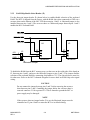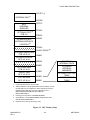
1
M68332BCC/D
REV 1
October 1993
M68332BCC
BUSINESS CARD COMPUTER
USER’S MANUAL
© MOTOROLA, INC., 1990, 1993; All Rights Reserved
Motorola reserves the right to make changes without further notice to any products herein to
improve reliability, function or design. Motorola does not assume any liability arising out of the
application or use of any product or circuit described herein; neither does it convey any license
under its patent rights nor the rights of others. Motorola products are not designed, intended, or
authorized for use as components in systems intended for surgical implant into the body, or other
applications intended to support or sustain life, or for any other application in which the failure
of the Motorola product could create a situation where personal injury or death may occur.
Should Buyer purchase or use Motorola products for any such unintended or unauthorized
application, Buyer shall indemnify and hold Motorola and its officers, employees, subsidiaries,
affiliates, and distributors harmless against all claims, costs, damages, and expenses, and
reasonable attorney fees arising out of, directly or indirectly, any claim of personal injury or
death associated with such unintended or unauthorized use, even if such claim alleges that
Motorola was negligent regarding the design or manufacture of the part.
CPU32Bug is a trademark of Motorola Inc.
White Knight is a trademark of FreeSoft Company.
MacTerminal, Apple, and Macintosh are trademarks of Apple Computer, Inc.
IBM-PC is a registered trademark of International Business Machines Corporation.
The computer program stored in the read only memory of the device contains material
copyrighted by Motorola Inc., first published in 1989, and may be used only under a license such
as the License For Computer programs (Article 14) contained in Motorola Terms and Conditions
of Sale, Rev. 1/79.
TABLE OF CONTENTS
TABLE OF CONTENTS
CHAPTER 1 GENERAL INFORMATION
1.1
1.2
1.3
1.4
1.5
Introduction......................................................................................................................... 1-1
Features............................................................................................................................... 1-1
Specifications...................................................................................................................... 1-2
General Description ............................................................................................................ 1-3
Equipment Required ........................................................................................................... 1-4
CHAPTER 2 HARDWARE PREPARATION AND INSTALLATION
2.1
2.2
2.3
Introduction......................................................................................................................... 2-1
Unpacking Instructions....................................................................................................... 2-1
Hardware Preparation ......................................................................................................... 2-1
2.3.1 VSTBY Select Header (J1) ...................................................................................... 2-5
2.3.2 RAM Chip Enable Select Header (J2)...................................................................... 2-6
2.3.3 EPROM Chip Select Header (J3)............................................................................. 2-7
2.3.4 TxD Select Header (J4) ............................................................................................ 2-8
2.3.5 RxD Select Header (J5)............................................................................................ 2-9
2.3.6 Clock Input Select Header (J6)............................................................................... 2-10
2.4 Installation Instructions .................................................................................................... 2-12
2.4.1 Power Supply - BCC Interconnection .................................................................... 2-12
2.4.2 Terminal - BCC Interconnection............................................................................ 2-13
2.4.3 Target System - BCC Interconnection ................................................................... 2-15
CHAPTER 3 OPERATING INSTRUCTIONS
3.1
3.2
Introduction......................................................................................................................... 3-1
Limitations.......................................................................................................................... 3-1
3.2.1 Chip Select Usage .................................................................................................... 3-2
3.2.2 Other MCU Resources Used by CPU32Bug............................................................ 3-4
3.3 Operating Procedure ........................................................................................................... 3-5
3.4 Monitor Description............................................................................................................ 3-6
3.4.1 Memory and Register Display and Modification Commands.................................. 3-7
3.4.2 Breakpoint Capabilities ............................................................................................ 3-7
3.4.3 System Calls ............................................................................................................. 3-8
3.4.4 Diagnostic Monitor................................................................................................. 3-10
M68332BCC/D
REV 1
i
MOTOROLA
TABLE OF CONTENTS
CHAPTER 3 OPERATING INSTRUCTIONS (continued)
3.5
3.6
Assembling/Disassembling Procedure ............................................................................. 3-12
Downloading Procedures.................................................................................................. 3-16
3.6.1 Apple Macintosh (with MacTerminal) to BCC...................................................... 3-17
3.6.2 Apple Macintosh (with White Knight) to BCC...................................................... 3-19
3.6.3 IBM-PC (with KERMIT) to BCC .......................................................................... 3-20
3.6.4 IBM-PC (with PROCOMM) to BCC..................................................................... 3-22
CHAPTER 4 FUNCTIONAL DESCRIPTION
4.1 Introduction......................................................................................................................... 4-1
4.2 BCC Description................................................................................................................. 4-1
4.2.1 MCU......................................................................................................................... 4-2
4.2.1.1 32-Bit Central Processor Unit ......................................................................... 4-3
4.2.1.2 Time Processor Unit........................................................................................ 4-3
4.2.1.3 Queued Serial Module..................................................................................... 4-3
4.2.1.4 Random Access Memory ................................................................................ 4-4
4.2.1.5 External Bus Interface ..................................................................................... 4-4
4.2.1.6 Chip Selects..................................................................................................... 4-4
4.2.1.7 System Clock................................................................................................... 4-4
4.2.1.8 Test Module..................................................................................................... 4-5
4.2.2 User Memory............................................................................................................ 4-5
4.2.3 Terminal and Host Computer I/O Port ..................................................................... 4-5
4.2.4 Background Mode Interface Port ............................................................................. 4-5
CHAPTER 5 SUPPORT INFORMATION
5.1
5.2
Introduction......................................................................................................................... 5-1
Connector Signal Descriptions ........................................................................................... 5-1
APPENDIX A S-RECORD INFORMATION
M68332BCC/D
REV 1
ii
MOTOROLA
TABLE OF CONTENTS
LIST OF ILLUSTRATIONS
Figure
2-1
2-2
2-3
2-4
2-5
4-1
4-2
Page
BCC Jumper Header and Connector Location Diagram .................................................... 2-2
BCC to DB-9 Cable Schematic Diagram ......................................................................... 2-13
BCC to DB-25 Cable Schematic Diagram ....................................................................... 2-14
Expansion Connectors Pin Assignments .......................................................................... 2-16
Target System Expansion Connector Installation Dimensions ........................................ 2-17
BCC Block Diagram........................................................................................................... 4-2
BCC Memory Map ............................................................................................................. 4-6
LIST OF TABLES
Table
1-1
1-2
2-1
2-2
3-1
3-2
3-3
3-4
5-1
5-2
5-3
5-4
Page
BCC Specifications............................................................................................................. 1-2
External Equipment Requirements ..................................................................................... 1-4
Jumper Header Types ......................................................................................................... 2-3
Jumper Header Summary ................................................................................................... 2-3
BCC Rev. A Chip Selection Summary............................................................................... 3-2
BCC Rev. B Chip Selection Summary ............................................................................... 3-3
BCC Rev. C Chip Selection Summary ............................................................................... 3-3
CPU32Bug Exception Vectors ........................................................................................... 3-4
P1 Expansion Connector Pin Assignments ........................................................................ 5-1
P2 Expansion Connector Pin Assignments ........................................................................ 5-4
J8 Background Mode Connector Pin Assignments ............................................................ 5-7
J9 RS-232C Serial Communication Connector Pin Assignments ...................................... 5-8
M68332BCC/D
REV 1
iii
MOTOROLA
TABLE OF CONTENTS
M68332BCC/D
REV 1
iv
MOTOROLA
GENERAL INFORMATION
CHAPTER 1
GENERAL INFORMATION
1.1 INTRODUCTION
This manual provides general information, hardware preparation, installation instructions,
functional description, and support information for the M68332BCC Business Card Computer
(hereafter referred as BCC). Appendix A contains BCC downloading S-record information.
1.2 FEATURES
The BCC is a single-board computer complete with these features:
• MC68332 Microcontroller Unit (MCU)
• 64k x 16 bit, two erasable programmable read only memories (EPROMs).
Programmed into the BCC EPROMs is the M68CPU32BUG Debug Monitor. Refer to
the M68CPU32BUG Debug Monitor User's Manual, M68CPU32BUG/AD1.
• 32k x 16 bit, byte addressable random access memory (RAM)
• RS-232C compatible terminal/host computer input/output (I/O) port
• Background mode interface port
• EVS expansion connectors
• 2.25 x 3.875 in. (5.7 x 9.84 cm) PCB
The BCC can be used as a stand-alone evaluation module or can be connected directly to a target
system. The BCC is primarily intended to be used with a terminal or host computer. When using
a host computer, a user must have a terminal emulation package for BCC downloading
operations.
M68332BCC/D
REV 1
1-1
MOTOROLA
GENERAL INFORMATION
1.3 SPECIFICATIONS
Table 1-1 lists the BCC specifications.
Table 1-1. BCC Specifications
CHARACTERISTICS
Internal Clock
External Clock
Memory
32k x 16 RAM
64k x 16 EPROM
Terminal/Host I/O Port
SPECIFICATIONS
32.768 kHz
25 kHz to 50 kHz(1)
85ns (3 clock bus cycle access @
16.7 MHz)
200ns (5 clock bus cycle access @
16.7 MHz)
RS-232C compatible (with internal DC-DC converters for
+/-10 volts, 10 mA)
Temperature
Operating
Storage
Relative humidity
+25° C
-40 to +85° C
0 to 90% (non-condensing)
Power Requirements
Power Supply
Battery Backup
+5 Vdc @ 200 milliamps (min.)
+3 Vdc @ 50 microamps (min.)
Dimensions
2.25 x 3.875 in. (5.7 x 9.84 cm)
1. An optional high frequency clock source (as high as 16.77 MHz) may be used if MODCK
(P2, pin 28) is pulled to a logic low level. A hybrid oscillator is recommended as the
external clock.
M68332BCC/D
REV 1
1-2
MOTOROLA
GENERAL INFORMATION
1.4 GENERAL DESCRIPTION
Using the BCC, the user can design, debug, and evaluate MC68332 Microcontroller Unit (MCU)
based target systems. The BCC simplifies user evaluation of prototype hardware/software
products. The BCC requires a user-supplied power supply and an RS-232C compatible terminal
for functional operation.
The BCC can operate as a standalone single board computer, or as a well-defined core in larger
applications. Mounted on the BCC is a microcontroller, on-board memory, and a serial level
converter circuit.
Two 64-pin expansion connectors provide access to the MC68332 pins. Background mode
operation and RS-232C serial communication are available through the 64-pin expansion
connectors. Additional connectors also provide background mode operation and RS-232C serial
communication. See Chapter 5 for interface connector pin assignments.
The BCC is factory tested and shipped with factory installed jumpers. These jumpers allow the
user to customize the BCC functionality when special design considerations are required.
The M68CPU32BUG Debug Monitor (CPU32Bug) is programmed into the BCC EPROMs.
CPU32Bug is a software evaluation and debug tool which may be used to develop systems built
around the MCU. Using the debug monitor, the user interacts with the BCC through pre-defined
monitor commands which are entered at the terminal/host computer keyboard. These commands
perform functions such as modification of memory, modification of MCU internal registers,
program execution under various levels of control, and access to various I/O peripherals in the
MCU itself.
To program the BCC EPROMs you must remove the EPROMs and use an EPROM programmer.
M68332BCC/D
REV 1
1-3
MOTOROLA
GENERAL INFORMATION
1.5 EQUIPMENT REQUIRED
Table 1-2 lists the external equipment requirements for BCC operation.
Table 1-2. External Equipment Requirements
EXTERNAL EQUIPMENT
A terminal or host computer (RS-232C compatible) with a terminal emulation package
(PCKERMIT, PROCOMM, MacTerminal, White Knight, etc.)(1)
RS-232C serial communication cable for the terminal or host computer(2).
+5 Vdc at 200 mA power supply(2)
1.
Refer to Chapter 3 for details on downloading using a host computer with terminal emulation
package.
2. Refer to Chapter 2 for details.
M68332BCC/D
REV 1
1-4
MOTOROLA
HARDWARE PREPARATION AND INSTALLATION
CHAPTER 2
HARDWARE PREPARATION AND INSTALLATION
2.1 INTRODUCTION
This chapter provides unpacking instructions, hardware preparation, and installation instructions
for the BCC prior to target system installation. This description ensures the BCC is properly
configured for target system operation.
2.2 UNPACKING INSTRUCTIONS
Unpack the BCC from shipping carton. Refer to the packing list and verify that all items are
present. Save packing material for storing and shipping the BCC.
NOTE
If the product arrives damaged, save all packing material, and contact the
carrier’s agent.
2.3 HARDWARE PREPARATION
This portion of text describes the inspection and preparation of the BCC prior to installation and
ensures the proper configuration for target system operation. The BCC was factory tested and
shipped with factory-installed jumpers (Figure 2-1 shows jumper header and connector
locations). These jumper headers allow the user to customize BCC functionality. Table 2-1 is a
description of the BCC jumper header types, and Table 2-2 is a summary of the BCC jumper
headers.
CAUTIONS
Use caution when handling the BCC; the signals are not buffered so the BCC
is sensitive to static discharge.
Depending on the application, it may be necessary to cut wiring trace shorts
(cut-trace shorts) on the PCB. Be careful not to cut adjacent PCB wiring
traces.
M68332BCC/D
REV 1
2-1
MOTOROLA
HARDWARE PREPARATION AND INSTALLATION
64-Pin Expansion Connector
P1
Background Mode
Connector
J5 J4
J7
TxD
Select
J1
J6
Clock Input
Select
RxD
Select
RS-232C Serial
Communication
J2
J3
VSTBY
Select
RAM Chip
Select
EPROM Chip
Select
J8
P2
64-Pin Expansion Connector
Figure 2-1. BCC Jumper Header and Connector Location Diagram
M68332BCC/D
REV 1
2-2
MOTOROLA
HARDWARE PREPARATION AND INSTALLATION
Table 2-1. Jumper Header Types
Jumper Header
Type (1)
Symbol
Description
three-pin with jumper
Three-pin jumper header with jumper and designated as JX (X =
the jumper header number). To change the factory jumper header
configuration, move the jumper to the two desired pins.
two-pin with jumper
Two-pin jumper header with jumper, designated as JX (X = the
jumper header number).
1. J7 and J8 are designated as jumper headers but they are in fact connectors.
Table 2-2. Jumper Header Summary
Jumper
Header
J1(1)
Type
2
1
Description
Jumper between pins 1 and 2 (factory default); disables (grounds) the on-board
RAM (U1 & U3) voltage standby power (VSTBY) input pin. VSTBY maintains
the data in RAM if BCC power (+5Vdc) is turned off.
No jumper; enables the on-board RAM VSTBY function. The VSTBY voltage
must be supplied by the user.
J2(1)
3
2
1
Jumper between pins 1 and 2 (factory default); enables the on-board RAM
chips (U1 & U3).
Jumper between pins 2 and 3; disables the on-board RAM chips. This allows
the chip select to be used with off-board memory.
J3(1)
3
2
1
Jumper between pins 1 and 2 (factory default); enables the on-board EPROM at
U2.
Jumper between pins 2 and 3; disables the on-board EPROM at U2. This allows
the chip select to be used to boot from off-board memory.
J4(1)
2
1
Jumper between pins 1 and 2 (factory default); connects the on-board transmit
data serial communication drivers to the MC68332 MCU device.
No jumper; disconnects the on-board transmit data serial communication drivers
from the MC68332 MCU device. This allows connection of the MCU serial port
to off board logic.
1. These jumper headers are shorted by a trace on the solder side of the PCB (between the pins), as
shown in the schematics. Cut the trace when using the optional feature provided by the jumper.
M68332BCC/D
REV 1
2-3
MOTOROLA
HARDWARE PREPARATION AND INSTALLATION
Table 2-1. Jumper Header Summary (continued)
Jumper
Header
Type
J5(1)
Description
Jumper between pins 1 and 2 (factory default); connects the on-board receive
data serial communication drivers to the MC68332 MCU device.
2
1
No jumper; disconnects the on-board receive data serial communication drivers
from the MC68332 MCU device. This allows connection of the MCU serial port
to off board logic.
J6(1)
Jumper between pins 1 and 2; selects an external clock source for the
MC68332 MCU device.
3
2
1
Jumper between pins 2 and 3 (factory default); selects the on-board oscillator
as the MC68332 MCU device clock source.
J7
10
8
6
4
2
J8
9
7
5
3
1
4
3
2
1
10-pin background mode connector.
4-pin RS-232C serial connector.
1. These jumper headers are shorted by a trace on the solder side of the PCB (between the pins), as
shown in the schematics. Cut the trace when using the optional feature provided by the jumper.
M68332BCC/D
REV 1
2-4
MOTOROLA
HARDWARE PREPARATION AND INSTALLATION
2.3.1
VSTBY Select Header (J1)
Use the two-pin jumper header J1 (shown below) to select a voltage standby (VSTBY) power
supply source. VSTBY provides battery backup to the RAM contained in the MC68332 MCU
device. The BCC is shipped from the factory with VSTBY connected to ground (GND) via J1
cut-trace short. To power VSTBY with an external supply, cut the trace on the bottom of the
PCB and connect an external power supply between P1, pin 28 and any BCC ground pin. Refer
to the BCC schematic diagram for more detail on VSTBY signal wiring.
64-Pin Expansion Connector
P1
28
Fabricated Jumper
VSTBY
19
2
U5
1
J1
GND
VSTBY
MC68332 MCU
NOTE
If the cut-trace short on jumper header J1 is cut, a user-supplied fabricated
jumper must be installed on J1 to return the BCC to its default setting.
M68332BCC/D
REV 1
2-5
MOTOROLA
HARDWARE PREPARATION AND INSTALLATION
2.3.2
RAM Chip Enable Select Header (J2)
Use the three-pin jumper header J2 (shown below) to enable/disable selection of the on-board
RAM. The BCC is shipped from the factory with the RAM chip select connected to GND via a
cut-trace short on the bottom of the BCC PCB between pins 1 and 2. A fabricated jumper is also
installed between pins 1 and 2. The cut-trace short or a fabricated jumper between pins 1 and 2
enables the BCC on-board RAM.
BR/CS0
BGACK/CS2
BG/CS1
+5V
3
J2
2
GND 1
U4
U3
27
WE
22 OE
20 CS
27
WE
22
OE
20
CS
MCM6206
MCM6206
Fabricated Jumper
To disable the RAM from the BCC memory map, cut the trace on the solder side of the board on
J2, between pins 1 and 2, and move the fabricated jumper to pins 2 and 3. This jumper disables
selection of the on-board RAM by connecting chip enable to +5V. The chip selects are now free
for other uses. Refer to the BCC schematic diagram for more detail on RAM chip select signal
wiring.
CAUTION
Do not connect the jumper between pins 2 and 3 before removing the cut-trace
short between pins 1 and 2. Installing the jumper before the cut-trace short is
removed connects +5Vdc to ground. If +5Vdc is shorted to ground the BCC or
power supply may be damaged.
NOTE
If the cut-trace short on jumper header J2 is cut, the fabricated jumper must be
reinstalled on J2, pins 1 and 2 to return the BCC to its default setting.
M68332BCC/D
REV 1
2-6
MOTOROLA
HARDWARE PREPARATION AND INSTALLATION
2.3.3
EPROM Chip Select Header (J3)
When BCC power is applied or reset occurs, the MC68332 MCU device resets itself and
downloads the program in EPROM (U1 & U2). The EPROM contains the boot program. Use the
three-pin jumper header J3 (shown below) to disable the BCC on-board EPROM. The BCC is
shipped from the factory with the EPROM connected to the MCU bootstrap chip select pin
(CSBOOT ) via a cut-trace short on the bottom of the BCC PCB between pins 1 and 2. A
fabricated jumper is also installed between pins 1 and 2. To boot from a program stored in
memory located in the target system, cut this trace, move the jumper to pins 2 and 3, and connect
CSBOOT to the target system via P2, pin 25. Cutting the cut-trace short and moving the
fabricated jumper to pins 2 and 3, removes U1 & U2 from the BCC memory map. Refer to the
BCC schematic diagram for more detail on CSBOOT signal wiring.
GND
Fabricated Jumper
+5V
U2
3
2
20
CS
22
OE/VPP
20
CS
22
OE/VPP
1
U5
27C512
J3
CSBOOT
U1
27C512
112
25
MC68332 MCU
P2
64-Pin Expansion Connector
CAUTION
Do not connect the jumper between pins 2 and 3 before removing the cut-trace
short between pins 1 and 2. Installing the jumper before the cut-trace short is
removed connects +5Vdc to (CSBOOT ). If +5Vdc is shorted to (CSBOOT )
the MCU may be damaged.
NOTE
If the cut-trace short on jumper header J3 is cut, the fabricated jumper must be
reinstalled on J3 pins 1 and 2 to return the BCC to its default setting.
M68332BCC/D
REV 1
2-7
MOTOROLA
HARDWARE PREPARATION AND INSTALLATION
2.3.4
TxD Select Header (J4)
Jumper header J4 allows the user to disconnect the transmit TxD serial data pin of the MC68332
MCU device (U5) from the RS-232C receiver/driver (U6) and use a target system
receiver/driver. The BCC is shipped from the factory with the receiver/driver connected to MCU
TxD (pin 52) via a cut-trace short on the bottom of the BCC PCB between J4, pins 1 and 2
(shown below). A fabricated jumper is also installed on pins 1 and 2. To disconnect the serial pin
of the MCU, cut this trace and remove the jumper.
64-Pin Expansion Connector
P1
53
TxD
Fabricated Jumper
U5
TxD
J4
52
U6
2
1
MC68332 MCU
15
XMT 232
DI1
TX1
6
MC145407
24
P2
64-Pin Expansion Connector
NOTE
If the cut-trace short on jumper header J4 is cut, the fabricated jumper must be
reinstalled on J4 to return the BCC to its default setting.
Refer to the BCC schematic diagram for more detail on TxD signal wiring.
M68332BCC/D
REV 1
2-8
MOTOROLA
HARDWARE PREPARATION AND INSTALLATION
2.3.5
RxD Select Header (J5)
Jumper header allows the user to disconnect the receive RxD serial data pin of the MC68332
MCU device (U5) from the RS-232C receiver/driver (U6) and use a target system
receiver/driver. The BCC is shipped from the factory with receiver/driver connected to MCU
RxD via a cut-trace short on the bottom of the BCC PCB between J5, pins 1 and 2 (shown
below). A fabricated jumper is also installed on pins 1 and 2. To disconnect the RxD pin of the
MCU, cut this trace and remove the jumper.
64-Pin Expansion Connector
P1
56
RxD
Fabricated Jumper
U5
RxD
J5
53
U6
2
1
MC68332 MCU
16
RCV 232
DO1
RX1
5
MC145407
26
P2
64-Pin Expansion Connector
NOTE
If the cut-trace short on jumper header J5 is cut, the fabricated jumper must be
reinstalled on J5 to return the BCC to its default setting.
Refer to the BCC schematic diagram for more detail on RxD signal wiring.
M68332BCC/D
REV 1
2-9
MOTOROLA
HARDWARE PREPARATION AND INSTALLATION
2.3.6
Clock Input Select Header (J6)
Use the three-pin jumper header J6 (shown below) to select the BCC on-board clock source or an
external clock source. The BCC on-board clock source is a 32 kHz crystal, which is frequency
multiplied by the MC68332 to a programmable operating frequency. The BCC is shipped with
the on-board crystal selected as the clock source. J6 has a cut-trace short on the bottom of the
BCC PCB between pins 2 and 3. A fabricated jumper is also supplied, but is not required when
the user uses the on-board clock source. Refer to the BCC schematic diagram for more detail on
EXTAL signal wiring.
U5
60
BCC
On-Board
Oscillator
XTAL
3
2
62
1
EXTAL
MC68332 MCU
J6
EXTAL
Fabricated Jumper
59
P2
64-Pin Expansion Connector
M68332BCC/D
REV 1
2-10
MOTOROLA
HARDWARE PREPARATION AND INSTALLATION
An optional high frequency oscillator (0 to 16.77 MHz) may be used if MODCK (connector P2,
pin 28) is pulled to a logic low level. To use the target-system, external-source CMOS clock;
follow these steps:
a. Turn off power to the BCC.
b. Cut the printed circuit trace on the bottom of the BCC between pins 2 and 3.
c. Move the fabricated jumper between pins 2 and 3 to pins 1 and 2.
d. Supply an external oscillator to connector P2, pin 59 (EXTAL).
e. Ground connector P2, pin 28 (MODCK).
f. Apply power to the BCC, start the external oscillator, and drive connector P1, pin 57
(RESET), low.
NOTES
If the cut-trace short on jumper header J6 is cut, the fabricated jumper must be
reinstalled on J6 pins 2 and 3 to return the BCC to its default setting.
Use a hybrid oscillator when driving the MCU from an external source.
Any change in the MC68332 MCU device clock speed causes a corresponding
change in the SCI baud rate. The operational speed of the MCU is determined
by the clock and the synthesizer control register value (SYNCR). The SCI
baud rate is then set based on this system clock frequency. If changes are
made to the MCU speed and the terminal baud rate is not changed
appropriately, terminal communication will fail. Refer to Appendix C of the
M68CPU32BUG Debug Monitor User’s Manual, M68CPU32BUG/AD1.
M68332BCC/D
REV 1
2-11
MOTOROLA
HARDWARE PREPARATION AND INSTALLATION
2.4 INSTALLATION INSTRUCTIONS
A user supplied power supply and RS-232C compatible terminal are required for BCC operation.
An RS-232C compatible host computer, with terminal emulation package, may be connected to
the BCC for S-record downloading.
2.4.1
Power Supply - BCC Interconnection
The BCC requires +5 Vdc @ 200 mA (max.) for operation. Use 18 to 20 AWG wire to connect a
user supplied power supply to the BCC. This connection is made via expansion connector P1 or
P2.
There are two preferred methods for connecting the power supply to the BCC: wire-wrap and
crimp-to-wire. When using the crimp-to-wire method, fabricate two wires (+5 Vdc and GND) as
follows:
a. Trim back 18 - 20 AWG wire approximately 0.25 inch.
b. Attach a crimp-to-wire receptacle (Dupont 46227-0000) to the wire using a crimping
tool.
c. Place heat shrink tubing (Digi-Key W183-ND) on the crimp-to-wire receptacle and
shrink using a heat source.
Connect the power supply ground fabricated wire to pin 1, 2, 63, or 64 of P1 or P2. Connect the
power supply +5 Vdc fabricated wire to pin 3, 4, 61, or 62 of P1 or P2 (as shown below).
P1/P2
M68332BCC/D
REV 1
GND
1
2
GND
+5V
3
4
+5V
5
6
59
60
+5V 61
62 +5V
GND 63
64 GND
2-12
MOTOROLA
HARDWARE PREPARATION AND INSTALLATION
2.4.2
Terminal - BCC Interconnection
Interconnection of an RS-232C compatible terminal to the BCC is accomplished via a user
supplied 9- or 25-conductor cable assembly as shown in Figures 2-2 and 2-3. If the user’s
terminal/host computer has a DB-9 connector refer to Figure 2-2. If the user’s terminal/host
computer has a DB-25 connector refer to Figure 2-3. One end of the cable assembly connects to
the BCC connector J9 (shown below). The other end of the cable assembly connects to the user
supplied terminal or host computer. For connector pin assignments and signal descriptions of
BCC terminal port connector J9, refer to Chapter 5.
1
2
3
4
J8
XMT 232
1
BCC
J8
2
3
4
XMT 232
GND
RCV 232
NC
GND
+10V
1
2
RCV 232
3
+10V
4
5
TERMINAL OR
HOST COMPUTER
6
NC
7
8
NC
9
Figure 2-2. BCC to DB-9 Cable Schematic Diagram
M68332BCC/D
REV 1
2-13
MOTOROLA
HARDWARE PREPARATION AND INSTALLATION
1
BCC
J8
2
3
4
XMT 232
NC
GND
RCV 232
NC
+10V
NC
NC
NC
NC
NC
NC
NC
NC
NC
NC
NC
NC
NC
NC
NC
NC
NC
1
2
3
4
5
6
7
8
9
10
11
12
13
14
15
16
17
18
19
20
21
22
23
24
25
TERMINAL OR
HOST COMPUTER
Figure 2-3. BCC to DB-25 Cable Schematic Diagram
M68332BCC/D
REV 1
2-14
MOTOROLA
HARDWARE PREPARATION AND INSTALLATION
2.4.3
Target System - BCC Interconnection
For target system to BCC interconnection the BCC mounts on the target system as shown below.
This configuration is used to evaluate the user’s hardware design. The 64-pin expansion
connectors provide access to most of the MC68332 MCU device pins. Figure 2-4 illustrates the
expansion header pin assignments for the BCC. Physical dimension requirements for installing
the BCC on a target system are illustrated in Figure 2-5.
M68332BCC
Connectors
for BCC
Target System
Target System to BCC Interconnection
M68332BCC/D
REV 1
2-15
MOTOROLA
HARDWARE PREPARATION AND INSTALLATION
P1
GND
1
P2
2
GN D
G ND
1
2
GND
+5V
3
4
+5V
+5V
3
4
+5V
DT RO UT
5
6
A0
D1
5
6
D0
A2
D3
7
8
D2
9
10
D4
A1
7
8
A3
9
10
A4
D5
A5
11
12
A6
D7
11
12
D6
A7
13
14
A8
D 9 13
14
D8
A9
15
16
A10
D 11 15
16
D10
A11
17
18
A12
D13 17
18
D12
A13
19
20
A14
D15 19
20
D14
A15
21
22
A16
RXD DI 21
22
TXD DI
A17
23
24
A18
M OD B DI 23
24
XMT 232
NC
25
26
NC
CSBOOT
25
26
RC V 232
13-24V DI
27
28
VST BY
R/W
27
28
MO DC K
13-24V DI
29
30
T2CLK
TST ME/TSC
29
30
A23/CS10
T P15
31
32
TP14
A22/CS9 31
32
A21/CS8
T P13
33
34
TP12
A20/CS7 33
34
A19/CS6
TP11
35
TP10
FC2/CS5 35
36
FC 1/CS4
T P9
37
TP8
FC0/CS3 37
38
BGAC K/CS2
TP6
BG/CS1 39
40
BR/CS0
TP4
IRQ1 41
42
IR Q2
44
IR Q4
T P7
T P5
39
41
36
38
40
42
T P3
43
44
TP2
IRQ3 43
T P1
45
46
TP0
IRQ5 45
46
IR Q6
MISO
IRQ7 47
48
BERR
DSACK0 49
50
DSACK1
51
52
RM C
D S 53
54
AS
SIZ 0 55
56
SIZ 1
57
58
CLKOUT
EXTAL 59
60
HALT
+5V 61
62
+5V
64
GND
MO SI
47
48
PC S0/SS
49
50
SC K
PC S2
51
52
PC S1
TXD
53
54
PC S3
BKPT /DSC LK
55
56
RXD
RESET
57
58
FREEZE/Q U OT
IPIPE/D SO
59
60
IFET CH/DSI
+5V
61
62
+5V
GND
63
64
GN D
AVEC
11R ESET
G ND
63
Figure 2-4. Expansion Connectors Pin Assignments
M68332BCC/D
REV 1
2-16
MOTOROLA
HARDWARE PREPARATION AND INSTALLATION
.100 in.
2.54 mm
P1
P2
3.1 in.
7.87 cm
2 in.
5.08 cm
VIEW:
TOP
Figure 2-5. Target System Expansion Connector Installation Dimensions
M68332BCC/D
REV 1
2-17
MOTOROLA
HARDWARE PREPARATION AND INSTALLATION
M68332BCC/D
REV 1
2-18
MOTOROLA
OPERATING INSTRUCTIONS
CHAPTER 3
OPERATING INSTRUCTIONS
3.1 INTRODUCTION
The EPROMs on the BCC contain the M68CPU32BUG debug monitor program (hereafter
referred to as CPU32Bug). CPU32Bug is a software tool for evaluating and debugging systems
built around the MC68332 MCU. CPU32Bug allows loading, debugging, and executing of user
programs. Various CPU32Bug routines that handle I/O, data conversion, timer, and string
functions are available to user programs through system calls. For a detailed description of the
CPU32Bug functions, refer to M68CPU32BUG Debug Monitor User’s Manual,
M68CPU32BUG/AD1.
CPU32Bug consists of:
• Memory and register display and modification commands
•
Breakpoint capabilities
•
System calls
•
Diagnostic commands
•
A single-line assembler/disassembler
There are two modes of operation in the CPU32Bug monitor; the debugger mode and the
diagnostic mode. When the user is in the debugger directory the prompt CPU32Bug> appears,
and the user has access to the debugger commands (refer to paragraph 3.4). When the user is in
the diagnostic mode the prompt CPU32Diag> appears, and the user has access to the diagnostic
commands (refer to paragraph 3.4.4). These modes are also called directories.
CPU32Bug is command-driven and performs various operations in response to user commands
entered at the keyboard. CPU32Bug executes entered commands; upon completion the prompt
reappears. However, if a command is entered which causes execution of user target code (i.e.,
GO), control may or may not return to CPU32Bug. This depends upon the user program
function. Entering the help (HE) command provides a list of all possible commands and their
structure.
3.2 LIMITATIONS
CPU32Bug requires some system resources to operate properly: chip selects, level 7 interrupt,
software watchdog timer, periodic interrupt timer, and system exception vectors.
M68332BCC/D
REV 1
3-1
MOTOROLA
OPERATING INSTRUCTIONS
3.2.1
Chip Select Usage
The MC68332 MCU has chip select signals that enable peripheral devices. The BCC requires
some of these chip selects for BCC operation making them unavailable to the user. Do not
remove the chip selects used by the BCC, or CPU32Bug will not operate. In addition to the chip
selects employed on the BCC, other chip selects are used elsewhere in the M68332EVK (refer to
Tables 3-1 through 3-3).
Depending on the user’s environment, any or all of the chip selects may be re-configured for an
alternate function (i.e., as I/O or address lines). Chip select pins used by the BCC and EVK
cannot be used in their alternate capacities.
Although a chip select (CS8 on Rev. A and CS4 on Rev. B and Rev. C BCCs) is dedicated for
the ABORT switch, the pin is not used. Instead the chip select decodes the interrupt acknowledge
(IACK) cycle in response to a level 7 interrupt generated by the ABORT switch. Refer the
System Integration Module User’s Manual (SIM32UM/AD) for more information.
When the BCC is not mounted on the M68300PFB Platform Board (PFB), these chip selects are
available to the user. Also if the PFB RAM/EPROM socket pairs (U1/U3, U2/U4) and
coprocessor socket U5 are not populated, the chip selects are available to the user.
Table 3-1. BCC Rev. A Chip Selection Summary
Signal
Board/Chip
Description
Memory Type
CSBOOT
BCC U2
CPU32Bug EPROM
CS0
BCC U1
read/write enable for MSB=UPPER=EVEN
RAM
CS1
BCC U3
read/write enable for LSB=LOWER=ODD
RAM
CS2
PFB U1/U3
read enable for MSB/LSB=BOTH
RAM
CS3
PFB U1
write enable for LSB=LOWER=ODD
RAM
CS4
PFB U4
read enable for MSB=UPPER=EVEN
RAM/EPROM
CS5
PFB U2
read enable for LSB=LOWER=ODD
RAM/EPROM
CS6
PFB U5
chip enable for MC68881/882
CS7
<unused>
CS8
PFB
CS9
<unused>
CS10
PFB U3
M68332BCC/D
REV 1
ABORT push-button autovector
write enable for MSB=UPPER=EVEN
cut/jump U3-27 from CS4 to CS10 required.
3-2
RAM
MOTOROLA
OPERATING INSTRUCTIONS
Table 3-2. BCC Rev. B Chip Selection Summary
Signal
Board/Chip
CSBOOT
CS0
CS1
CS2
CS3
CS4
CS5
BCC U2
BCC U1
BCC U3
BCC U3/U1
<unused>
PFB
PFB U5
CS6
CS7
CS8
CS9
CS10
PFB U2
PFB U4
PFB U1/U3
PFB U1
PFB U3
Description
CPU32Bug EPROM
write enable for MSB=UPPER=EVEN
write enable for LSB=LOWER=ODD
read enable for MSB/LSB=BOTH
ABORT push-button autovector
chip enable for MC68881/882. cut/-jump U5-J3
from CS2 to CS5 required.
read enable for LSB=LOWER=ODD
read enable for MSB=UPPER=EVEN
read enable for MSB/LSB=BOTH
write enable for LSB=LOWER=ODD
write enable for MSB=UPPER=EVEN
Memory Type
RAM
RAM
RAM
RAM/EPROM
RAM/EPROM
RAM
RAM
RAM
Table 3-3. BCC Rev. C Chip Selection Summary
Signal
Board/Chip
CSBOOT
CSBOOT
CS0
CS1
CS2
CS3
CS4
CS5
BCC U3
BCC U4
BCC U1
BCC U2
BCC U3/U1
<unused>
PFB
PFB U5
CS6
CS7
CS8
CS9
CS10
PFB U2
PFB U4
PFB U1/U3
PFB U1
PFB U3
M68332BCC/D
REV 1
Description
Memory Type
CPU32Bug EPROM for MSB=UPPER=EVEN
CPU32Bug EPROM for LSB=LOWER=ODD
write enable for MSB=UPPER=EVEN
write enable for LSB=LOWER=ODD
read enable for MSB/LSB=BOTH
RAM
RAM
RAM
ABORT push-button autovector
chip enable for MC68881/882. cut/-jump U5-J3
from CS2 to CS5 required.
read enable for LSB=LOWER=ODD
read enable for MSB=UPPER=EVEN
read enable for MSB/LSB=BOTH
write enable for LSB=LOWER=ODD
write enable for MSB=UPPER=EVEN
RAM/EPROM
RAM/EPROM
RAM
RAM
RAM
3-3
MOTOROLA
OPERATING INSTRUCTIONS
3.2.2
Other MCU Resources Used by CPU32Bug
Avoid writing the value zero to bit 7 of the port F pin assignment register (PFPAR); such a value
disables the ABORT switch.
The software watchdog timer is disabled via a write-once register (SYPCR) during power-up or
reset, so the software watchdog timer cannot be used or re-enabled by the user unless the user
modifies the SYPCR_OR and SYPCR_AND parameters. Modification of the SYPCR_OR and
SYPCR_AND parameters is detailed in Appendix C of the M68CPU32BUG Debug Monitor
User’s Manual, M68CPU32BUG/AD1.
The monitor uses the system exception vectors, so they are unavailable to the BCC user. The
monitor debug exception vectors are listed in Table 3-4. The associated debugger facilities
(breakpoints, trace mode, etc.) will not operate if the vector offsets in the target program vector
table are changed.
Table 3-4. CPU32Bug Exception Vectors
Vector
Number
Offset
4
$10
Illegal
Instruction breakpoints (Used by GO, GN, GT)
9
$24
Trace
T, TC, TT
31
$7C
Level 7 interrupt
ABORT switch
47
$BC
TRAP #15
System calls (see Chapter 5 of the M68CPU32BUG
Debug Monitor User’s Manual, M68CPU32BUG/AD1)
66
$108
User Defined
Timer Trap #15 Calls ($4X)
Exception
CPU32Bug Commands
Any change in the MC68332 MCU device clock speed causes a corresponding change in the SCI
baud rate. The operational speed of the MCU is determined by the clock and the synthesizer
control register value (SYNCR) or by an external clock signal applied to the EXTAL pin of the
MCU. The SCI baud rate is then set based on this system clock frequency. If changes are made to
the MCU system clock frequency, changes must be made to the customization parameter area
(FCRYSTAL or FEXTAL) so the correct baud rate can be calculated for SCI communications by
CPU32Bug. See the M68CPU32BUG Debug Monitor User’s Manual (M68CPU32BUG/AD1),
Appendix C for details.
Additionally, CPU32Bug writes a one (1) to the module mapping (MM) bit of the module
control register (MCR). This configures the register block to start at address $FFF000. As the
MM bit is a write-once bit, the user cannot clear it to move the register block to low memory
($7FF000). The user can move the register block by modifying the MCR_AND parameter
detailed in Appendix C of the M68CPU32BUG Debug Monitor User’s Manual,
M68CPU32BUG/AD1.
M68332BCC/D
REV 1
3-4
MOTOROLA
OPERATING INSTRUCTIONS
3.3 OPERATING PROCEDURE
A Power On Reset (POR) occurs when power is applied to the BCC. This POR condition resets
the MCU and user I/O port circuitry. After a POR occurs, processing control passes to the
monitor program. All MC68332 registers are set to their reset state during monitor power-up.
The input serial format for the BCC terminal I/O port must be configured for 8 data bits, 1 stop
bit, no parity, and 9600 baud.
The terminal then displays this message:
CPU32Bug Debugger/Diagnostics - Version X.XX
(C) Copyright 1989, 1990 by Motorola Inc.
CPU32Bug>
where:
X.XX is the software revision level
After initialization or return of control to the monitor, the terminal displays the prompt
"CPU32Bug>" and waits for a response. If an incorrect response is entered, the terminal displays
"Invalid command" followed by the prompt "CPU32Bug>".
CPU32Bug waits for a command line input from the user terminal. When a proper command is
entered, the operation continues in one of two basic modes. If the command causes execution of
a user program, the monitor may or may not be reentered, depending upon the desire of the user.
For the alternate case, the command is executed under the control of the monitor, and the system
returns to a waiting condition after the command is completed. During command execution,
additional user input may be required, depending on the command function.
The user can use any of the commands supported by the monitor. A standard input routine
controls the BCC operation while the user types a command line. Command processing begins
only after the command line has been terminated by pressing the keyboard carriage return <CR>
key.
M68332BCC/D
REV 1
3-5
MOTOROLA
OPERATING INSTRUCTIONS
3.4 MONITOR DESCRIPTION
CPU32Bug performs various operations in response to user commands entered at the keyboard.
When the debugger prompt CPU32Bug> appears on the terminal screen, the debugger is ready
to accept commands.
As the command line is entered it is stored in an internal buffer. Execution begins only after the
carriage return is entered. This lets the user correct entry errors using the control characters
described in the M68CPU32BUG Debug Monitor User’s Manual, M68CPU32BUG/AD1.
After the debugger executes a command it returns with the CPU32Bug> prompt. However, if the
entered command causes execution of user target code, (i.e., GO), then control may or may not
return to the debugger. This depends on the user program function. For example, if a breakpoint
is specified, control returns to the debugger when the breakpoint is encountered during user
program execution. The user program also returns control to the debugger by means of the TRAP
#15 system call function, .RETURN.
Included as part of the CPU32Bug firmware is a single-line assembler/disassembler function.
The assembler is an interactive assembler/editor in which source programs are not saved. Each
source line is translated into MC68332 MCU machine language code and stored line-by-line into
memory as it is entered. In order to display an instruction, the machine code is disassembled and
the instruction mnemonic and operands are displayed. All valid MC68332 MCU instructions are
supported.
The CPU32Bug assembler is effectively a subset of the M68000 Family Structured Assembler
(M68MASM). It has some limitations as compared with the M68MASM assembler, such as not
allowing line numbers and labels; however, it is a useful tool for creating, modifying, and
debugging MC68332 MCU code.
M68332BCC/D
REV 1
3-6
MOTOROLA
OPERATING INSTRUCTIONS
3.4.1
Memory and Register Display and Modification Commands
Various commands are available to the user for displaying and modifying memory. For more
information, refer to Chapter 3 of the M68CPU32BUG Debug Monitor User’s Manual,
M68CPU32BUG/AD1. The memory display and modification commands are:
3.4.2
•
BF (block of memory fill) fills the specified range of memory with a data pattern.
•
BM (block of memory move) copies the contents of the memory addresses defined by
<RANGE> to another place in memory, beginning at <ADDR>.
•
BS (block of memory search) searches the specified range of memory for a match
with a user-entered data pattern.
•
BV (block of memory verify) compares the specified range of memory against a data
pattern.
•
MD (memory display) displays the contents of multiple memory locations.
•
MM (memory modify) examines and changes memory locations.
•
MS (memory set) writes data to memory starting at a specified address.
•
RD (register display) displays the contents of the MCU registers.
•
RM (register modify) examines and changes register contents.
•
RS (register set) writes data to a specified register.
Breakpoint Capabilities
A breakpoint lets the user set a target code instruction address stopping point for debugging
purposes. Target code execution halts when a breakpoint is encountered. For more information
on breakpoints, refer to Chapter 3 of the M68CPU32BUG Debug Monitor User's Manual,
M68CPU32BUG/AD1. The breakpoint commands are:
•
BR/NOBR (breakpoint insert/delete) allows the user to set/remove a target code
instruction address as a breakpoint address for debugging purposes.
•
GD (go direct) starts target code execution and ignores breakpoints.
•
GN (go to temporary breakpoint) sets a temporary breakpoint at the address of the
next instruction, that is, the one following the current instruction.
•
GT (go to temporary breakpoint) sets a temporary breakpoint at the current
instruction and starts target code execution.
•
TT (trace to temporary breakpoint) sets a temporary breakpoint at a specified address
and traces until encountering a breakpoint.
M68332BCC/D
REV 1
3-7
MOTOROLA
OPERATING INSTRUCTIONS
3.4.3
System Calls
The CPU32Bug TRAP #15 handler allows system calls from user programs. A system call
accesses selected functional routines contained in CPU32Bug, including input and output
routines. TRAP #15 also transfers control to CPU32Bug at the end of a user program. For more
information on system calls, refer to Chapter 5 of the M68CPU32BUG Debug Monitor User’s
Manual, M68CPU32BUG/AD1. System calls include:
•
.INCHR (input character) reads a character from the default input port.
•
.INSTAT (input serial port status) checks for characters in the default input port
buffer.
•
.INLN (input line (pointer/pointer format)) reads a line from the default input port.
•
.READSTR (input string (pointer/count format)) reads a string of characters from the
default input port into a buffer.
•
.READLN (input line (pointer/count format)) reads a string of characters from the
default input port.
•
.CHKBRK (check for break) returns zero (0) status in condition code register if break
status is detected at the default input port.
•
.OUTCHR (output character) outputs a character to the default output port.
•
.OUTSTR (output string in pointer/pointer format) outputs a string of characters to
the default output port.
•
.OUTLN (output line in pointer/pointer format) outputs a character strings followed
by a carriage return (<CR>) and a line feed (<LF>) sequence.
•
.WRITE (output string in pointer/count format) formats character strings with a
count byte and outputs the string to the default output port. After formatting, the
count byte is the first byte in the string.
•
.WRITELN (output line in pointer/count format) formats character strings with a
count byte and outputs the string to the default output port. After formatting, the
count byte is the first byte in the string.
•
.PCRLF (output carriage return and line feed) sends a <CR> and a <LF> sequence to
the default output port.
•
.ERASLN (erase line) erases the line at the present cursor position.
•
.WRITD (output string with data in pointer/count format) uses the monitor I/O
routine which outputs a user string containing embedded variable fields. The user
passes the starting address of the string and the data stack address containing the data
which is inserted into the string. The output goes to the default output port.
M68332BCC/D
REV 1
3-8
MOTOROLA
OPERATING INSTRUCTIONS
•
.WRITDLN (output line with data in pointer/count format) uses the monitor I/O
routine which outputs a user string containing embedded variable fields. The user
passes the starting address of the string and the data stack address containing the data
which is inserted into the string. The output goes to the default output port.
•
.SNDBRK (send break) sends a break to the default output port.
•
.TM_INI (timer initialization) initializes the MC68331 MCU device periodic
interrupt timer.
•
.TM_STR0 (start timer at T=0) resets the timer to zero and starts it.
•
.TM_RD (read timer) reads the timer count.
•
.DELAY (timer delay) generates timing delays.
•
.RETURN (return to CPU32Bug) returns control to CPU32Bug from the target
program.
•
.BINDEC (convert binary to Binary Coded Decimal) calculates the BCD equivalent
of a specified binary number.
•
.CHANGEV (parse value) parses value in user specified buffer.
•
.STRCMP (compare two strings in pointer/count format) compares equality and
returns a Boolean flag to the caller.
•
.MULU32 (multiply two 32-bit unsigned integers) multiplies two 32-bit unsigned
integers and returns the product on the stack as a 32-bit unsigned integer.
•
.DIVU32 (divide two 32-bit unsigned integers) divides two 32-bit unsigned integers
and returns the quotient on the stack as a 32-bit unsigned integer.
M68332BCC/D
REV 1
3-9
MOTOROLA
OPERATING INSTRUCTIONS
3.4.4
Diagnostic Monitor
The diagnostic monitor is a series of self-tests for the MC68332 MCU device. The diagnostic
monitor is programmed into the BCC EPROM. For more information on the diagnostic monitor,
refer to Chapter 6 of the M68CPU32BUG Debug Monitor User’s Manual,
M68CPU32BUG/AD1. The diagnostic monitor commands are:
•
HE (help) command displays a menu of the top level directory.
•
ST (self test) command executes self-test diagnostics.
•
SD (switch directories) command toggles between the CPU32Bug directory and the
CPU32Diag directory.
•
LE (loop-on-error) endlessly repeats a test at the point where an error is detected.
•
SE (Stop-On-Error) halts a test at the point where an error is detected.
•
LC (loop-continue) endlessly repeats a test or series of tests.
•
NV (non-verbose)suppresses all error messages except PASSED or FAILED.
•
DE (display error counters) displays the results of a particular test.
•
ZE (clear error counters) resets all error counters to zero.
•
DP (display pass count) is the number of passes in loop-continue mode. Under this
command the count is displayed with other information at the conclusion of each
pass.
•
ZP (zero pass count) resets the pass counter to zero.
Available utilities are:
– WL - Write Loop
– RL - Read Loop
– WR - Read/Write Loop
CPU tests are a series of diagnostics provided to test the CPU portion of the MC68332
MPU:
– CPU A - Register Test
– CPU B - Instruction Test
– CPU C - Address Mode Test
– CPU D - Exception Processing Test
M68332BCC/D
REV 1
3-10
MOTOROLA
OPERATING INSTRUCTIONS
Memory tests are a series of diagnostics that verify random access memory (read/write)
that may reside on the BCC.
– MT A - Set Function Code
– MT B - Set Start Address
– MT C - Set Stop Address
– MT D - Set Bus Data Width
– MT E - March Address Test
– MT F - Walk a Bit Test
– MT G - Refresh Test
– MT H - Random Byte Test
– MT I - Program Test
– MT J - TAS Test
Bus error test (BERR) tests for internal bus access time-out and internal to external bus
access time-out error conditions, including:
– Bus errors when accessing the BCC RAM.
– Bus errors when reading the BCC EPROM.
– Bus errors when accessing the PFB optional memory.
– Internal bus access time-outs when reading and writing from an undefined function
code/memory location internal to the MCU.
– Internal to external bus access time-outs reading or writing to an undefined
function code/memory location external to the MCU.
M68332BCC/D
REV 1
3-11
MOTOROLA
OPERATING INSTRUCTIONS
3.5 ASSEMBLING/DISASSEMBLING PROCEDURE
The assembler/disassembler is an interactive, one-line assembler/editor in which the source
program is not saved. Each source line is converted into machine language code and is stored in
memory on a line-by-line basis at the time of entry. In order to display an instruction, the
machine code is disassembled and the instruction mnemonic and operands are displayed. All
valid opcodes are converted to assembly language mnemonic. All invalid opcodes return a
Declare Constant Word (DC.W) conversion.
The memory modify (mm ;di) command lets the user create, modify, and debug MC68332 MCU
code. Assembler input must have exactly one space between the mnemonic and the operand.
There must be no space inside the operand field. Assembler input must be terminated by a
carriage return. No comments are allowed after the instruction input and no line labels are
permitted.
After each new assembler input line, the new line is disassembled for the user before stepping to
the new instruction. The new line may assemble to a different number of bytes than the previous
one.
For Branch if Higher or Same (BHS)/Branch if Carry Clear (BCC) mnemonics, disassembly
displays the BCC mnemonic. For Branch if Lower (BLO)/Branch if Carry Set (BCS)
mnemonics, disassembly displays the BCS mnemonic.
Branch address offsets are automatically calculated by the assembler, so the user should input the
destination address rather than an offset value.
The assembler is terminated by entering a period (.) followed by a carriage return as the only
entry on the command input line. Entering a carriage return alone on an input line steps to the
next instruction.
The following pages describe how to operate the assembler/disassembler by creating a typical
program loop, and debugging the program using CPU32Bug monitor commands. A typical
program loop is first assembled. Routine examples then illustrate how to set a breakpoint,
proceed from a breakpoint, display and modify registers, and initiate user program execution.
M68332BCC/D
REV 1
3-12
MOTOROLA
OPERATING INSTRUCTIONS
Enter the periodic interrupt timer (PIT) time-out program starting at address $5000:
EXAMPLE
PROGRAM
PROGRAM
DESCRIPTION
Memory modify at location $5000 with
disassembly option.
Set-up level six vector table.
Initialize PIT.
Execute LPSTOP Instruction.
Loop
Beginning of message.
End of message.
Check for SCI not busy.
Branch until free.
Send message byte.
Check for end of message.
Branch until done.
Return from print routine.
CPU32Bug>MM 5000;DI<CR>
5000
5008
5012
5018
501C
5020
5024
502C
502E
5034
5036
503A
MOVE.L #$501C,$78<CR>
MOVE.L #$061E0120,$FFFA22<CR>
LPSTOP #$2500<CR>
BRA.W $5012<CR>
MOVEA.W #$5100,A0<CR>
MOVEA.W #$510E,A1<CR>
BTST.B #$0,$FFFC0C<CR>
BEQ.B $5024<CR>
MOVE.B (A0)+,$FFFC0F<CR>
CMPA.W A0,A1<CR>
BNE.W $5024<CR>
RTE<CR>
Enter the ASCII code for the output message, PIT TIME-OUT. Each time this message appears
when running the program, indicates the program has completed a loop. Enter the following
ASCII code at memory location $5100:
CPU32Bug>MS 5100 ’PIT TIME-OUT’ODOA<CR>
M68332BCC/D
REV 1
3-13
Memory modify at location $5100.
MOTOROLA
OPERATING INSTRUCTIONS
After entering the PIT time-out program display the instructions at location $5000
EXAMPLE
PROGRAM
PROGRAM
DESCRIPTION
Display memory at location $5000 with
disassembly option.
CPU32Bug>MD 5000;DI<CR>
5000
5008
21FC0000
23FC061E
FA22
5012
F80001C0
5018
6000FFF8
501C
307C5100
5020
327C510E
5024
08390000
502C
67F6
CPU32Bug><CR>
502E
13D800FF
5034
B2C8
5036
6600FFEC
503A
4E73
503C
0000FFFF
5040
0000FFFF
5044
0000FFFF
5048
0000FFFF
501C0078
012000FF
2500
00FFFC0C
MOVE.L
#$501C,($78).W
MOVE.L
LPSTOP.W
BRA.W
MOVEA.W
MOVEA.W
BTST.B
BEQ.B
#$061E0120,($FFFA22).L
#$2500
$5012
#$5100,A0
#$510E,A1
#$0,($FFFC0C).L
$5024
MOVE.B
CMPA.W
BNE.W
RTE
ORI.B
ORI.B
ORI.B
ORI.B
(A0)+,(FFFC0F).L .
A0,A1
$5024
Display next eight instructions.
FC0F
#$FF,D0
#$FF,D0
#$FF,D0
#$FF,D0
The message displayed on the terminal
CPU32Bug>MD 5100<CR>
00005100 5049 5420 5449 4D45
M68332BCC/D
REV 1
2D4F 5554 0D0A FFFF
3-14
PIT TIME-OUT....
MOTOROLA
OPERATING INSTRUCTIONS
The following routines are performed on the preceding program loop:
ROUTINE
DESCRIPTION
TERMINAL
CPU32Bug>MD 5000;DI<CR>
00005000
21FC0000 501C0078
00005008
23FC061E 012000FF
FA22
00005012
F80001C0 2500
00005018
6000FFF8
0000501C
307C5100
00005020
327C510E
00005024
08390000 00FFFC0C
0000502C
67F6
CPU32Bug>MM 500C<CR>
0000500C
0120? 00FF.
CPU32Bug>g 5000<CR>
Effective address: 00005000
PIT TIME-OUT
PIT TIME-OUT
PIT TIME-OUT
:
:
Display memory at address 5000
MOVE.L
#$501C,($78).W
MOVE.L
LPSTOP.W
BRA.W
MOVEA.W
MOVEA.W
BTST.B
BEQ.B
#$061E0120, (FFFA22)
#$2500
$5012
#$5100,A0
#$510E,A1
#$0,($FFFC0C).L
$5024
Modify memory at location 500C.
Change PIT time-out speed.
Go to address 5000 and begin execution.
Periodic interrupt timer time-out message.
Press the ABORT switch on the PFB to terminate the loop program.
Exception: ABORT
PC
=00005018
SR
=2500=TR:OFF_S_5_.....
SFC
=5=SD
DFC
=5=SD
USP
=0000FC00
D0
=00000000
D1
=00000000
D2
=00000000
D4
=00000000
D5
=00000000
D6
=00000000
A0
=0000510E
A1
=0000510E
A2
=00000000
A4
=00000000
A5
=00000000
A6
=00000000
00005018
6000FFF8
BRA.W.W
$5012
CPU32Bug>T 1<CR>
Trace one instruction.
PC
=00005018
SR
=2500=TR:OFF_S_5_.....
SFC
=5=SD
DFC
=5=SD
USP
=0000FC00
D0
=00000000
D1
=00000000
D2
=00000000
D4
=00000000
D5
=00000000
D6
=00000000
A0
=0000510E
A1
=0000510E
A2
=00000000
A4
=00000000
A5
=00000000
A6
=00000000
00005012
F80001C0
2500
LPSTOP.W
#$2500
CPU32Bug>BR 5034<CR>
Set breakpoint at 5034.
BREAKPOINTS
00005034
CPU32Bug>g 5000<CR>
Go to address 5000 and begin
Effective address: 00005018
At Breakpoint
PC
=00005034
SR
=2600=TR:OFF_S_6_.....
SFC
=5=SD
DFC
=5=SD
USP
=0000FC00
D0
=00000000
D1
=00000000
D2
=00000000
D4
=00000000
D5
=00000000
D6
=00000000
A0
=00005101
A1
=0000510E
A2
=00000000
A4
=00000000
A5
=00000000
A6
=00000000
00005034
B2C8
CMPA.W
A0,A1
M68332BCC/D
REV 1
3-15
VBR
SSP*
D3
D7
A3
A7
=00000000
=00010000
=00000000
=00000000
=00000000
=00010000
VBR
SSP*
D3
D7
A3
A7
=00000000
=00010000
=00000000
=00000000
=00000000
=00010000
execution.
VBR
SSP*
D3
D7
A3
A7
=00000000
=0000FFF8
=00000000
=00000000
=00000000
=0000FFF8
MOTOROLA
OPERATING INSTRUCTIONS
3.6 DOWNLOADING PROCEDURES
Downloading transfers information from a host computer to the BCC, via the load (LO)
command. The procedure described below lets the user download with an IBM personal
computer (PC) or Apple Macintosh host computer.
The LO command moves data in S-record format (see Appendix A) from an external host
computer to the EVK user pseudo ROM.
Subsections 3.6.1 through 3.6.4 list instructions for downloading to the EVK from an Apple
Macintosh with MacTerminal or Red Ryder, or from an IBM-PC with Kermit or PROCOMM.
M68332BCC/D
REV 1
3-16
MOTOROLA
OPERATING INSTRUCTIONS
3.6.1
Apple Macintosh (with MacTerminal) to BCC
The MacTerminal downloading program serves as a terminal emulator for the Apple Macintosh
computer. To download a Motorola S-record file from the Apple Macintosh computer to the
BCC:
a. Select the following menu Terminal Settings:
Terminal:
VT100
Mode:
ANSI
Cursor Shape:
Underline
Line Width:
80 Columns
Select:
On Line
Auto Repeat
Click on:
OK
b. Select the following menu Compatibility Settings:
Baud rate:
9600
Bits per Character:
8 Bits
Parity:
None
Handshake:
XOn/XOff
Connection:
Another Computer
Connection Port:
Modem
Click on:
OK
c. Select the following menu File Transfer Settings:
M68332BCC/D
REV 1
Settings for Pasting
or Sending Text:
Word Wrap Outgoing Text
File Transfer
Protocol:
Text
Settings for Saving
Lines Off Top:
Retain Line Breaks
Click on:
OK
3-17
MOTOROLA
OPERATING INSTRUCTIONS
d. Apply power to the BCC.
e. Press Apple Macintosh computer keyboard carriage return (<CR>) key to display
applicable BCC monitor prompt.
f
Apple Macintosh computer displays the CPU32Bug> prompt.
g. Enter BCC monitor download command as follows:
CPU32Bug>LO<CR>
h. Operate pull-down File menu, and select (choose): Send File ...
i. Use dialog box and select applicable S-record object file.
Click on:
Send
Motorola S-record file is now transferred to the BCC.
NOTE
S-record file will not be displayed during the file
transfer to the BCC.
The underline cursor flashes and the beeper sounds when the S-record has finished
downloading. Press the carriage return twice to return to the CPU32Bug prompt:
<CR>
<CR>
CPU32Bug>
M68332BCC/D
REV 1
3-18
MOTOROLA
OPERATING INSTRUCTIONS
3.6.2
Apple Macintosh (with White Knight) to BCC
The White Knight downloading program serves as a terminal emulator for the Apple Macintosh
computer. To download a Motorola S-record file from the Apple Macintosh computer to the
BCC:
a. Execute White Knight program.
b. Set up computer program to match BCC baud rate (typically) as follows:
9600 baud, no parity, 8-bits, 1-stop bit, full duplex
c. Apply power to BCC.
d. Press Apple Macintosh computer keyboard carriage return (<CR>) key to display
applicable BCC monitor prompt.
e
Enter BCC monitor download command as follows:
CPU32Bug>LO<CR>
f. Operate pull-down File menu, and select (choose):
Send File - ASCII...
g. Use dialog box and select applicable S-record object file.
Click on:
Send
Motorola S-record file is now transferred to the BCC.
NOTE
S-record file will not be displayed during the file
transfer to the BCC.
The underline cursor flashes and the beeper sounds when the S-record has finished
downloading. Press the carriage return twice to return to the CPU32Bug prompt:
<CR>
<CR>
CPU32Bug>
M68332BCC/D
REV 1
3-19
MOTOROLA
OPERATING INSTRUCTIONS
3.6.3
IBM-PC (with KERMIT) to BCC
Before performing any IBM-PC operation, ensure that both IBM-PC and BCC baud rates are
9600, and that the IBM-PC asynchronous port is configured for terminal mode of operation. If
the asynchronous port is hard wired for host mode of operation and cannot be re-configured for a
terminal mode of operation, the use a null modem (cross-coupled transmit (TxD), and receive
(RxD), and associated handshake lines) is required.
NOTE
IBM-PC to BCC connection requires one serial communication cable assembly.
This cable is connected to the BCC terminal I/O port connector J9 for
downloading operations.
To perform IBM-PC to BCC downloading procedure:
EXAMPLE
DESCRIPTION
C>KERMIT<CR>
IBM-PC Kermit-MS VX.XX
Type ? for help
IBM-PC prompt. Enter Kermit program.
Kermit-MS>SET BAUD 9600<CR>
Kermit-MS>CONNECT<CR>
Set IBM-PC baud rate.
Connect IBM-PC to BCC.
[Connecting to host, type Control-] C to return to PC]
<CR>
CPU32Bug>LO<CR>
BCC download command (via terminal
port) entered.
(CTRL)]C
Kermit-MS>PUSH<CR>
The IBM Personal Computer DOS
Version X.XX (C)Copyright IBM Corp. 1981, 1982, 1983
C>TYPE (File Name) > COM1<CR>
Motorola S-record file name.
C>EXIT<CR>
S-record downloading completed.
Kermit-MS>CONNECT<CR>
Return to BCC monitor program.
M68332BCC/D
REV 1
3-20
MOTOROLA
OPERATING INSTRUCTIONS
The underline cursor flashes and the beeper sounds when the S-record has finished downloading.
Press the carriage return twice to return to the CPU32Bug prompt:
<CR>
<CR>
CPU32Bug>
CPU32Bug>(CTRL) ]C
KERMIT-MS>EXIT<CR>
M68332BCC/D
REV 1
Exit Kermit program.
3-21
MOTOROLA
OPERATING INSTRUCTIONS
3.6.4
IBM-PC (with PROCOMM) to BCC
To perform the IBM-PC to BCC downloading procedure with PROCOMM:
a. Execute the PROCOMM.EXE program.
b. Setup PROCOMM to match BCC baud rate and protocol (type (Alt)P, then the
number 11) as follows:
9600 baud, no parity, 8 bits, 1 stop bit, full duplex
c. Setup ASCII transfer parameters (type (Alt)S, then the number 6) as follows:
Echo Local - No
Expand Blank Lines - Yes
Pace Character - 0
Character pacing - 15 (milliseconds)
Line Pacing - 10
CR Translation - None
LF Translation - None
Save above settings to disk for future use.
d. Apply power to BCC.
e. Press IBM-PC keyboard carriage return (<CR>) key to display applicable BCC
monitor prompt.
f
Enter BCC monitor download command as follows:
CPU32Bug>LO<CR>
g. Instruct PROCOMM to send the S-record file by pressing the Pg Up key on the PC,
then follow PROCOMM instructions on the display screen to select the S-record file
using an ASCII protocol.
Motorola S-record file is transferred to the BCC when the beeper sounds and the
underline cursor flashes. Press the carriage return twice to return to the CPU32Bug
prompt:
<CR>
<CR>
CPU32Bug>
M68332BCC/D
REV 1
3-22
MOTOROLA
FUNCTIONAL DESCRIPTION
CHAPTER 4
FUNCTIONAL DESCRIPTION
4.1 INTRODUCTION
This chapter provides a functional description of the BCC. This description is supported by a
block diagram (Figure 4-1) and a memory map diagram (Figure 4-2). Refer to Chapter 5 for the
BCC schematic diagram.
4.2 BCC DESCRIPTION
The MC68332 Microcontroller Unit (MCU) resident on the BCC provides resources for
designing, debugging, and evaluating MC68332 MCU based target systems and simplifies user
evaluation of prototype hardware/software products.
Figure 4-1 is a block diagram of these BCC circuits:
• MCU
• User memory
• Terminal and host computer I/O port
• Background mode interface port
M68332BCC/D
REV 1
4-1
MOTOROLA
FUNCTIONAL DESCRIPTION
TIMER CHANNELS
TERMINAL/
HOST
COMPUTER
P4
RS-232C
INTERFACE
U5
P1
ADDRESS AND CONTROL LINES
MCU
U1
BACKGROUND MODE
P3
64K x 8
EPROM
U1
64K x 8
EPROM
U2
32K x 8
RAM
U3
32K x 8
RAM
U4
INTERRUPT SIGNALS
P2
DATA AND CONTROL LINES
Figure 4-1. BCC Block Diagram
4.2.1
MCU
The resident MC68332 Microcontroller Unit (MCU) of the BCC provides resources for
designing, debugging, and evaluating MC68332 MCU based target systems and simplifies user
evaluation of prototype hardware/software products.
The MCU device is a 32-bit integrated microcontroller, combining high-performance data
manipulation capabilities with powerful peripheral subsystems. The MCU includes:
• 32-bit central processor unit (CPU32)
• Time processor unit (TPU)
• Queued serial module (QSM)
• Random access memory (RAM)
• External bus interface
• Chip selects
• System clock
• Test module
M68332BCC/D
REV 1
4-2
MOTOROLA
FUNCTIONAL DESCRIPTION
4.2.1.1
32-Bit Central Processor Unit
The CPU32 is the central processor for the MC68332 MCU device. The CPU32 is source and
object code compatible with the MC68000 and MC68010. All user programs can be executed
unchanged. The CPU32 features are:
• 32-Bit internal data path and arithmetic hardware - 16-bit external data bus
• 32-Bit internal address bus - 24-bit external address bus
• Powerful instruction set
• Eight 32-bit general purpose data registers
• Seven 32-bit general purpose address registers
• Separate user and supervisor stack pointers and address spaces
• Separate program and data address spaces
• Flexible addressing modes
• Full interrupt processing
4.2.1.2
Time Processor Unit
The Time Processor Unit (TPU) optimizes performance of time-related activities. The TPU has a
dedicated execution unit, tri-level prioritized scheduler, data storage RAM, dual time bases, and
microcode ROM which drastically reduces the need for CPU intervention. The TPU controls
sixteen independent, orthogonal channels; each channel has an associated I/O pin and can
perform any time function. Each channel also contains a dedicated event register, for both match
and input capture functions.
Each channel can be synchronized to either of two 16-bit, free-running counters with a pre-scaler.
One counter, based on the system clock, provides resolution of TPU system clock divided by 4.
The second counter, based on an external reference, also provides resolution of TPU system
clock divided by 8. Channels may also be linked together, allowing the user to reference
operations on one channel to the occurrence of a specified action on another channel, providing
inter-task control.
4.2.1.3
Queued Serial Module
The QSM contains two serial ports. The queued serial peripheral interface (QSPI) port provides
easy peripheral expansion or inter-processor communications via a full-duplex, synchronous,
three-line bus: data-in, data-out, and a serial clock. Four programmable peripheral select pins
provide address-ability for as many as 16 peripheral devices. A QSPI enhancement is an added
queue in a small RAM. This lets the QSPI handle as many as 16 serial transfers of 8- to 16-bits
each, or to transmit a stream of data as long as 256 bits without CPU intervention. A special
wrap-around mode lets the user continuously sample a serial peripheral, automatically updating
the QSPI RAM for efficient interfacing to serial peripheral devices (such as analog-to-digital
converters).
M68332BCC/D
REV 1
4-3
MOTOROLA
FUNCTIONAL DESCRIPTION
The serial communications interface (SCI) port provides a standard non-return to zero (NRZ)
mark/space format. Advanced error detection circuitry catches noise glitches to 1/16 of a bit time
in duration. Word length is software selectable between 8- or 9-bits, and the SCI modulus-type,
baud rate generator provides baud rates from 64 to 524k baud, based on a 16.77 MHz system
clock. The SCI features full- or half-duplex operation, with separate transmitter and receiver
enable bits and double buffering of data. Optional parity generation and detection provide either
even or odd parity check capability. Wake-up functions let the CPU run uninterrupted until either
a true idle line is detected or a new address byte is received.
4.2.1.4
Random Access Memory
2k bytes of static RAM are contained within the MC68332 MCU device. The RAM is used for
storage of variable and temporary data. RAM data size may be 8-bits (byte), 16-bits (word), or
32-bits (longword). The RAM can be mapped to any 2k byte boundary in the address map.
4.2.1.5
External Bus Interface
The external bus consists of 24 address lines and a 16-bit data bus. The data bus allows dynamic
sizing between 8- and 16-bit data accesses. A read-modify-write cycle (RMC) signal prevents
bus cycle interruption. External bus arbitration is accomplished by a three-line handshaking
interface.
4.2.1.6
Chip Selects
Twelve independently programmable chip selects provide fast, two-cycle external memory, or
peripheral access. Block size is programmable from 2 kilobytes through 1 megabyte. Accesses
can be selected for either 8- or 16-bit transfers. As many as 13 wait states can be programmed for
insertion during the access. All bus interface signals are automatically handled by the chip select
logic.
4.2.1.7
System Clock
An on-chip phase locked loop circuit generates the system clock signal to run the device up to
16.78 MHz from a 32.768 kHz watch crystal. The system speed can be changed dynamically,
providing either high performance or low power consumption under software control. The
system clock is a fully-static CMOS design, so it is possible to completely stop the system clock
via a low power stop instruction, while still retaining the contents of the registers and on-board
RAM.
M68332BCC/D
REV 1
4-4
MOTOROLA
FUNCTIONAL DESCRIPTION
4.2.1.8
Test Module
The test module consolidates the microcontroller test logic into a single block to facilitate
production testing, user self-test, and system diagnostics. Scan paths throughout the MC68332
provide signature analysis checks on internal logic. User self-test is initiated by asserting the test
pin to enter test mode. This test provides a pass/fail response to various externally supplied test
vectors.
4.2.2
User Memory
On board the BCC is 32k x 16 bits of RAM and 64k x 16 bits of EPROM. The RAM is the
debug monitor storage area and user accessible memory space; the M68CPU32BUG Debug
Monitor is stored in the BCC EPROMs. For debug monitor functionality see the
M68CPU32BUG Debug Monitor User’s Manual, M68CPU32BUG/AD1. Figure 4-3 is the EVK
memory map.
The PFB has sockets for 32k x 16 or 64k x 16 bit RAM or 64k x 16 bit EPROM. The RAM
and/or EPROM, supplied by the user, is user-accessible memory space.
4.2.3
Terminal and Host Computer I/O Port
The MC68332 MCU serial communication interface pins drive levels are 0 and 5 Vdc. An
interface device (U5) translates these voltage levels to +/-10 Vdc, sufficient to allow RS-232C
communications.
The RS-232C serial communication port P4 facilitates terminal and host computer
interconnection. If a host computer is used a terminal emulation package (PCKERMIT.EXE,
PROCOMM, MacTerminal, White Knight, etc.) must be utilized. Chapter 5 contains a
description of P4 pin assignments.
4.2.4
Background Mode Interface Port
The background debug mode is implemented in MCU microcode. In background mode, registers
can be viewed or altered, memory can be read or written, and test features can be executed.
Background mode is initiated by one of several sources: externally generated breakpoints,
internal peripherally generated breakpoints, software, and catastrophic exception conditions.
Instruction execution is suspended for the duration of background mode. Background mode
communications between the BCC and the development system are via a serial link (P3).
M68332BCC/D
REV 1
4-5
MOTOROLA
FUNCTIONAL DESCRIPTION
XXX7FF
INTERNAL RAM
(2)
(1 )
XXX000
FFFFFF
MCU
INTERNAL
MODULES
FFF000
OPTIONAL FPCP (3)
PFB: U5
FFE800
800000
ALTERNATE MCU
INTERNAL MODULES
LOCATION (4)
7FF000
OPTIONAL RAM/EPROM
PFB: U2 & U4
CPU32BUG EPROM
BCC: U1 & U2
110000 /120000 (5)
100000
0E0000
OPTIONAL RAM
PFB: U1 & U3
TARGET RAM
BCC: U3 & U4
SYSTEM RAM
BCC: U3 & U4
CPU32BUG
INTERNAL STACK
CPU32BUG
INTERNAL
VARIABLES
CPU32BUG VECTOR
TABLE
TARGET VECTOR
TABLE
020000
010000
003000
000000
1.
Consult the MCU device user’s manual.
2.
XXbase address is user programmable. Internal modules, such as
internal RAM, can be configured on power-up/reset by using the
initilization table (INITTBL) covered in Appendix C of the
M68CPU32BUG Debug Monitor User’s Manual,
M68CPU32BUG/AD1.
3.
Floating point coprocessor - MC68881/MC68882.
4.
See Appendix C of the M68CPU32BUG Debug Monitor User’s
Manual, M68CPU32BUG/AD1.
5.
Depends on the memory device type used.
Figure 4-2. BCC Memory Map
M68332BCC/D
REV 1
4-6
MOTOROLA
SUPPORT INFORMATION
CHAPTER 5
SUPPORT INFORMATION
5.1 INTRODUCTION
This chapter provides the connector signal descriptions.
5.2 CONNECTOR SIGNAL DESCRIPTIONS
Connectors P1 and P2 connect the BCC to a target system. Connector P3 is for background
mode. Connector P4 is for serial communication between the BCC and a host computer.
Pin assignments for P1, P2, P3 and P4 are defined in Tables 5-1 through 5-4. Connector signals
are identified by pin number, signal mnemonic, and signal name and description.
Table 5-1. P1 Expansion Connector Pin Assignments
Signal Mnemonic
Pin Number
Signal Name And Description
1, 2
GND
GROUND
3, 4
+5V
SYSTEM POWER SUPPLY – +5 volt power source.
5
DTROUT
DATA TERMINAL READY – RS-232C handshake from
the BCCDI.
6 — 24
A0 — A18
ADDRESS BUS – Three-state output address bus.
25
NC
No Connection
26
NC
No Connection
27
+13—24V DI
M68332BCC/D
REV 1
+13—24 VOLTS DEVELOPMENT INTER-FACE –
BCCDI switching voltage.
5-1
MOTOROLA
SUPPORT INFORMATION
Table 5-1. P1 Expansion Connector Pin Assignments (continued)
Signal Mnemonic
Pin Number
Signal Name And Description
28
VSTBY
VOLTAGE STANDBY – Input standby voltage source
for MCU on-chip RAM.
29
+13—24V DI
30
T2CLK
31 — 46
TP15 — TP0
47
MOSI
MASTER-OUT SLAVE-IN – Serial output from the
OSPI in master mode, and serial input to the QSPI in
slave mode.
48
MISO
MASTER-IN SLAVE-OUT – Serial input to the QSPI in
master mode, and serial output from the QSPI in slave
mode.
49
PCS0 /
+13—24 VOLTS DEVELOPMENT INTERFACE –
BCCDI switching voltage.
TPU CLOCK – External input clock source to the TPU.
TIME PROCESSOR UNIT CHANNELS – TPU
Input/output channels.
PERIPHERAL CHIP SELECT 0 – Active-low output
QSPI peripheral chip select signal.
SS
SLAVE SELECT – Bi-directional active-low signal that
places the QSPI in slave mode.
50
SCK
QSPI SERIAL CLOCK – Input/output QSPI clock
source.
51
PCS2
PERIPHERAL CHIP SELECT 2 – Active-low output
QSPI peripheral chip select.
52
PCS1
PERIPHERAL CHIP SELECT 1 – Active-low output
QSPI peripheral chip select.
53
TXD
54
PCS3
M68332BCC/D
REV 1
TRANSMIT DATA – Serial data output line.
PERIPHERAL CHIP SELECT 3 – Active-low output
QSPI peripheral chip select.
5-2
MOTOROLA
SUPPORT INFORMATION
Table 5-1. P1 Expansion Connector Pin Assignments (continued)
Signal Mnemonic
Pin Number
55
Signal Name And Description
BKPT /
BREAKPOINT – An active-low input signal that places
the CPU32 in background debug mode.
DSCLK
DEVELOPMENT SYSTEM CLOCK – Serial input clock
for background debug mode.
56
RXD
57
RESET
58
FREEZE /
FREEZE – Output signal that indicates that the CPU32
has entered background debug mode.
QUOT
QUOTIENT OUT – Output signal that furnishes the
quotient bit of the polynomial divider for test purposes.
IPIPE /
INSTRUCTION PIPE – Active-low output signal used to
track movement of words through the instruction
pipeline.
59
DSO
60
IFETCH /
RECEIVE DATA – Serial data input line.
RESET – Active-low input/output signal for initiating a
system reset.
DEVELOPMENT SERIAL OUT – Serial output for
background debug mode.
INSTRUCTION FETCH – Active-low output signal that
indicates when the CPU is performing an instruction
word pre-fetch and when the instruction pipeline has
been flushed.
DSI
DEVELOPMENT SERIAL IN – Serial data input for
background debug mode.
61, 62
+5V
+5 VOLT INPUT POWER
63, 64
GND
GROUND
M68332BCC/D
REV 1
5-3
MOTOROLA
SUPPORT INFORMATION
Table 5-2. P2 Expansion Connector Pin Assignments
Signal Mnemonic
Pin Number
Signal Name And Description
1, 2
GND
GROUND
3, 4
+5V
+5 VOLT INPUT POWER
5 — 20
D0 — D15
21
RXD DI
RECEIVE DATA DEVELOPMENT INTER-FACE –
BCCDI receive data.
22
TXD DI
TRANSMIT DATA DEVELOPMENT INTER-FACE –
BCCDI transmit data.
23
MODB DI
MODE B DEVELOPMENT INTERFACE – BCCDI
mode B.
24
XMT 232
TRANSMIT DATA – Serial data output signal.
25
CSBOOT
BOOT CHIP SELECT – An active-low output chip
select.
26
RCV 232
RECEIVE DATA – Serial data input signal.
27
R/W
READ/WRITE – Active-high output signal that indicates
the direction of data transfer on the bus.
28
MODCK
CLOCK MODE SELECT – Active-high input signal that
selects the source of the internal system clock.
29
TSTME /
TEST MODE ENABLE – Active-low input signal that is
a hardware enable for test mode.
TSC
THREE STATE CONTROL – When TSC is 8 volts (1.6
X +5V), this input signal forces all output drivers to a
high-impedance state.
A23/CS10 ,
A22/CS9 ,
A21/CS8 ,
A20/CS7 ,
A19/CS6
ADDRESS BUS 19—23 – Three-state output address
bus.
30 — 34
M68332BCC/D
REV 1
DATA BUS – 16 bi-directional data pins.
CHIP SELECTS 6—10 – Output signals that select
peripheral/memory devices at programmed addresses.
5-4
MOTOROLA
SUPPORT INFORMATION
Table 5-2. P2 Expansion Connector Pin Assignments (continued)
Signal Mnemonic
Pin Number
35 — 37
Signal Name And Description
FC2/CS5 ,
FC1/CS4 ,
FC0/CS3
FUNCTION CODES – Three-state output signals that
identify the processor state and address space of the
current bus cycle.
CHIP SELECTS 3—5 – Output signals that select
peripheral/memory devices at programmed addresses.
38
39
40
BGACK /
BUS GRANT ACKNOWLEDGE – Active-low input
signal that indicates that an external device has
assumed control of the bus.
CS2
CHIP SELECT 2 – Output signal that selects
peripheral/ memory devices at programmed addresses.
BG /
BUS GRANT – Active-low output signal that indicates
that the current bus cycle is complete and the
MC68332 has relinquished the bus.
CS1
CHIP SELECT 1 – Output signal that selects
peripheral/ memory devices at programmed addresses.
BR /
BUS REQUEST – Active-low input signal that indicates
that an external device requires bus master-ship.
CS0
CHIP SELECT 0 – Output signal that selects
peripheral/ memory devices at programmed addresses.
41 — 47
IRQ1 — IRQ7
INTERRUPT REQUEST (1—7) – Seven active-low
input lines used to request MCU synchronous
interrupts. IRQ7 has the highest priority.
48
BERR
BUS ERROR – Active-low input signal that indicates
that an erroneous bus operation is being attempted.
M68332BCC/D
REV 1
5-5
MOTOROLA
SUPPORT INFORMATION
Table 5-2. P2 Expansion Connector Pin Assignments (continued)
Signal Mnemonic
Pin Number
Signal Name And Description
49, 50
DSACK0 ,
DSACK1
DATA AND SIZE ACKNOWLEDGE – Active-low input
signals that allow asynchronous data transfers and
dynamic bus sizing between the MC68332 and external
devices.
51
AVEC
AUTOVECTOR – Active-low input signal that requests
an automatic vector during an interrupt acknowledge
cycle.
52
RMC
READ-MODIFY-WRITE CYCLE – Active-low output
signal that identifies the bus cycle as part of an
indivisible read-modify-write operation.
53
DS
DATA STROBE – Active-low output signal, that during
a read cycle, indicates that an external device should
place valid data on the data bus. During the write cycle,
DS indicates that valid data is on the data bus.
54
AS
ADDRESS STROBE – Active-low output signal that
indicates that a valid address is on the address bus.
55, 56
SIZ0, SIZ1
TRANSFER SIZE – Active-low output signals that
indicate the number of bytes remaining to be
transferred during this cycle.
57
11RESET
Not connected.
58
CLKOUT
59
EXTAL
EXTERNAL CLOCK INPUT – External clock input for
the MC68332 MCU device.
60
HALT
HALT – Active-low input/output signal that suspends
external bus activity, to request a retry when used with
BERR , or for single-step operation.
61, 62
+5V
+5 VOLT INPUT POWER
63, 64
GND
GROUND
M68332BCC/D
REV 1
SYSTEM CLOCK OUT – Output signal that is the
MC68332 internal system clock.
5-6
MOTOROLA
SUPPORT INFORMATION
Table 5-3. J8 Background Mode Connector Pin Assignments
Signal Mnemonic
Pin Number
Signal Name And Description
1
DS
2
BERR
3
GND
4
BKPT /
BREAKPOINT – An active-low input signal that places
the CPU32 in background debug mode.
DSCLK
DEVELOPMENT SYSTEM CLOCK – Serial input clock
for background debug mode.
DATA STROBE – Active-low output signal, that during
a read cycle, indicates that an external device should
place valid data on the data bus. During the write cycle,
DS indicates that valid data is on the data bus.
BUS ERROR – Active-low input signal that indicates
that an erroneous bus operation is being attempted.
GROUND
5
GND
GROUND
6
FREEZE /
FREEZE – Output signal that indicates that the CPU32
has entered background debug mode.
QUOT
QUOTIENT OUT – Output signal that furnishes the
quotient bit of the polynomial divider for test purposes
7
RESET
RESET – Active-low input/output signal for initiating a
system reset.
8
IFETCH /
INSTRUCTION FETCH – Active-low output signal that
indicates when the CPU is performing an instruction
word pre-fetch and when the instruction pipeline has
been flushed.
DSI
DEVELOPMENT SERIAL IN – Serial data input for
background debug mode.
9
+5V
+5 VOLT INPUT POWER
10
IPIPE /
DSO
M68332BCC/D
REV 1
INSTRUCTION PIPE – Active-low output signal used to
track movement of words through the instruction
pipeline.
DEVELOPMENT SERIAL OUT – Serial output for
background debug mode.
5-7
MOTOROLA
SUPPORT INFORMATION
Table 5-4. J9 RS-232C Serial Communication Connector Pin Assignments
Signal Mnemonic
Pin Number
Signal Name And Description
1
XMIT
TRANSMIT DATA – RS-232C serial output data.
2
GND
GROUND
3
RCV
RECEIVE DATA – RS-232C serial input data.
4
+10V
+10 VOLTS DC – Output voltage that may be used to
drive RS-232C handshake lines.
M68332BCC/D
REV 1
5-8
MOTOROLA
APPENDIX A
APPENDIX A
S-RECORD INFORMATION
The S-record format for output modules was devised for the purpose of encoding programs or
data files in a printable format for transportation between computer systems. The transportation
process can thus be visually monitored and the S-records can be more easily edited.
S-RECORD CONTENT
When viewed by the user, S-records are essentially character strings made of several fields which
identify the record type, record length, memory address, code/data and checksum. Each byte of
binary data is encoded as a 2-character hexadecimal number; the first character representing the
high-order 4 bits, and the second the low-order 4 bits of the byte.
The five fields which comprise an S-record are shown below:
TYPE
RECORD LENGTH
ADDRESS
CODE/DATA
CHECKSUM
Where the fields are composed as follows:
Field
Printable
Characters
Contents
type
2
S-records type -- S0, S1, etc.
record
length
2
The count of the character pairs in the record, excluding type and
record length.
4,6,or 8
The 2-, 3-, or 4-byte address at which the data field is to be loaded
into memory.
address
code/data
0-n
From 0 to n bytes of executable code, memory-loadable data, or
descriptive information. For compatibility with teletypewriters, some
programs may limit the number of bytes to as few as 28 (56 printable
characters in the S-record).
checksum
2
The least significant byte of the one’s complement of the sum of the
values represented by the pairs of characters making up the records
length, address, and the code/data fields.
M68332BCC/D
REV 1
A-1
MOTOROLA
APPENDIX A
Each record may be terminated with a CR/LF/NULL. Additionally, an S-record may have an
initial field to accommodate other data such as line numbers generated by some time-sharing
systems. An S-record file is a normal ASCII text file in the operating system of origin.
Accuracy of transmission is ensured by the record length (byte count) and checksum fields.
S-RECORD TYPES
Eight types of S-records have been defined to accommodate the several needs of the encoding,
transportation and decoding functions. The various Motorola upload, download and other
records transportation control programs, as well as cross assemblers, linkers and other filecreating or debugging programs, utilize only those S-records which serve the purpose of the
program. For specific information on which S-records are supported by a particular program, the
user’s manual for the program must be consulted. 332Bug supports S0, S1, S2, S3, S7, S8, and
S9 records.
An S-record format module may contain S-records of the following types:
Type
Description
S0
The header record for each block of S-records, The code/data.field may contain any descriptive
information identifying the following block of S-records. The address field is normally zeros.
S1
A record containing code/data and the 2-byte address at which the code/data is to reside.
S2
A record containing code/data and the 3-byte address at which the code/data is to reside.
S3
A record containing code/data and the 4-byte address at which the code/data is to reside.
S5
A record containing the number of S1, S2, and S3 records transmitted in a particular block. This
count appears in the address field. There is no code/data field.
S7
A termination record for a block of S3 records, The address field may optionally contain the 4byte address of the instruction to which control is passed. There is no code/data field.
S8
A termination record for a block of S2 records. The address field may optionally contain the 3byte address of the instruction to which control is passed. There is no code/data field.
S9
A termination record for a block of S1 records. The address field may optionally contain the 2byte address of the instruction to which control is passed. If not specified, the first entry point
specification encountered in the object module input will be used. There is no code/data field.
Only one termination record is used for each block of S-records. S7 and S8 records are usually
used only when control is to be passed to a 3 or 4 byte address. Normally, only one header
record is used, although it is possible for multiple header records to occur.
M68332BCC/D
REV 1
A-2
MOTOROLA
APPENDIX A
S-RECORDS CREATION
S-record format files may be produced by dump utilities, debuggers, linkage editors, cross
assemblers or cross linkers. Several pro- grams are available for downloading a file in S-record
format from a host system to a microprocessor-based system.
EXAMPLE
Shown below is a typical S-record format module, as printed or displayed:
S00600004844521B
S1130000285F245F2212226A000424290008237C2A
S11300100002000800082629001853812341001813
S113002041E900084E42234300182342000824A952
S113003000144ED492
S9030000FC
The module consists of one S0 record, four S1 records, and an S9 record.
The S0 record is comprised of the following character pairs:
S0
S-record type S0, indicating that it is a header record.
06
Hexadecimal 06 (decimal 6), indicating that six character pairs (or ASCII bytes) follow.
00
00
Four-character, 2-byte, address field; zeros in this example.
48
44
52
ASCII H, D and R - "HDR".
1B
The checksum.
The first S1 record is explained as follows:
S1
S-record type S1, indicating that it is a code/data record to be loaded/verified at a 2-byte
address.
13
Hexadecimal 13 (decimal 19), indicating that 19 character pairs, representing 19 bytes
of binary data, follow.
00
00
Four-character, 2-byte, address field; hexadecimal address 0000, where the data which
follows is to be loaded.
M68332BCC/D
REV 1
A-3
MOTOROLA
APPENDIX A
The next 16 character pairs of the first S1 record are the ASCII bytes of the actual program
code/data. In this assembly language example, the hexadecimal opcodes of the program are
written in sequence in the code/data fields of the S1 records:
OPCODE
INSTRUCTION
285F
245F
2212
226A0004
24290008
237C
MOVE.L
MOVE.L
MOVE.L
MOVE.L
MOVE.L
MOVE.L
(A7)+,A4
(A7)+,A2
(A2),D1
4(A2),A1
FUNCTION(A1),D2
#FORCEFUNC,FUNCTION(A1)
(The balance of this code is continued in the code/data fields of the
remaining S1 records and stored in memory.)
2A
The checksum of the first S1 record.
The second and third S1 records also each contain $13 (19) character pairs and are ended with
checksums 13 and 52 respectively. The fourth S1 record contains 07 character pairs and has a
checksum of 92.
The S9 record is explained as follows:
S9
S-record type S9, indicating that it is a termination record.
03
Hexadecimal 03, indicating that three character pairs (3 bytes) follow.
00
00
The address field, zeros.
FC
The checksum of the S9 record.
Each printable character in an S-record is encoded in a hexadecimal (ASCII in this example)
representation of the binary bits which are actually transmitted. For example, the first S1 record
above is sent as:
TYPE
S
5
LENGTH
1
3
3
1
1
3
ADDRESS
3
1
3
0
3
3
0
0
3
CODE/DATA
0
0
3
0
0
3
2
0
3
8
2
3
CHECKSUM
5
8
3
F
5
4
•••
6
•••
2
3
A
2
4
1
0101 0011 0011 0001 0011 0001 0011 0011 0011 0000 0011 0000 0011 0000 0011 0000 0011 0010 0011 1000 0011 0101 0100 0110 ••• 0011 0010 0100 0001
M68332BCC/D
REV 1
A-4
MOTOROLA