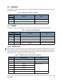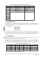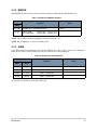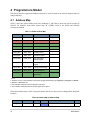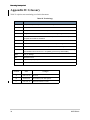
1
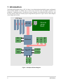
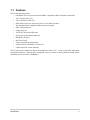
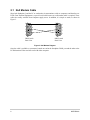
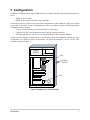
User’s Manual
SPX3BUM/D
Rev. 1.2, 2/2003
Sandpoint Microprocessor
Evaluation System
User’s Manual
Welcome to Sandpoint, Motorola’s flexible processor development platform. Using Sandpoint
you can evaluate current Motorola host processors and integrated processors based on the
PowerPC architecture using MPMC (Motorola Processor PCI Mezzanine Cards). These cards
are interchangable and one Sandpoint platform can support numerous processor-specific
PPMC cards (but just one at a time).
This user’s manual covers the following issues:
Topic
Section 1, “Introduction”
Section 2, “Setup”
Section 3, “Configuration”
Section 4, “Programmers Model”
Section 5, “Initializing Sandpoint”
Section 6, “Development Issues”
Section 7, “Troubleshooting”
Section 8, “FAQ”
Page
2
4
7
16
22
23
27
30
To locate any published errata or updates for this document, refer to the Motorola website.
1 Introduction
The Sandpoint III motherboard, or “SP3” for short, is an evaluation baseboard which accepts one Motorola
Processor PMC (MPMC) or PrPMC card, as well as up to four PCI cards, and supplies typical PC-I/O
peripherals. Sandpoint provides a flexible base for the evaluation of new Motorola processor devices, and
for early software design for customer project using Motorola processors. Figure 1 shows a block diagram
of the Sandpoint III system.
PCI Slots
KBD
Winbond
SuperIO
COM1
PAR
COM2
FLP
MSE
NVRM
IDE
ROM1
IDE
ROM2
Motorola
MPMC
Board
SPF100
Figure 1. Sandpoint III Block Diagram
2
MOTOROLA
1.1 Features
SP3 has the following features:
•
•
•
•
•
•
•
•
•
•
•
•
•
•
One MPMC slot for a processor board (PrPMC compatible with PCI arbitration extensions).
Two 32-bit PCI slots (5V)
Two 32/64-bit PCI slots (5V)
PMC and PCI slots auto-sense/auto-select 33 or 66 MHz operation.
Two standard 16650-compatible ESD-protected serial ports.
IEEE 1284 parallel port.
Floppy disk port.
Two ATA33 bus-master IDE ports.
PS/2 mouse and keyboard connectors.
BBVRAM; 8K bytes
Real-Time Clock.
Switch-selectable operating modes.
Advanced Power Controller (“soft on/off”).
LED monitors for critical functions.
The I/O subsystem is identical to that of the Sandpoint 2 and the “EC” version of the older Yellowknife
development platform. When properly configured, software written for these platforms should operate
identically when executed on a Sandpoint 3.
MOTOROLA
3
2 Setup
Sandpoint 3 is shipped ready to run the DINK debugger software. If you will be running other operating
systems, refer to the respective installation and setup instructions. Many OSes will communicate using the
same serial port DINK does, so the following setup may apply as well.
To setup your system, you will need the following material:
•
•
•
Sandpoint 3 system
Mac, PC or workstation running a terminal program.
Null-modem cable.
1
COM1
',1.!!JR
1
COM2
COM1
COM2
Figure 2. Sandpoint III Setup Diagram
STEP 1
Connect the Sandpoint to a 120 VAC source using the supplied AC power code. For international operation
at 240 VAC, replace the connector with an appropriately-keyed power cable.
STEP 2
Turn the power supply on using the switch at the back of the Sandpoint chassis near the power cord. The
system will not turn on at this time.
STEP 3
Attach a null-modem cable between the Sandpoint COM1 port (top-most as shown in Figure 2) to the PC
(or workstation) serial port (usually COM1).
STEP 4
Startup a terminal emulator program. Common terminal emulators include “Hyperterminal”, available for
free with most Windows PCs, and many commercial programs such as Hayes “SmartComm”. Setup the PCs
terminal program to use the following settings:
•
•
•
4
9600 Baud
8 Bits
No Parity
MOTOROLA
•
•
•
1 Stop Bit
No Handshaking
Terminal Emulation: any
STEP 5
Turn on the Sandpoint by pushing the power switch on the front of the chassis. DINK will start and print a
banner:
###### ### #
# #
# #####
#
# # ##
# # # #
#
#
# # # #
# # #
#
#
# # # # # ##
#####
#
# # #
# # # #
#
#
# # #
## # # #
#
###### ### #
# #
# #####
(
(
( ( (AltiVec) ) )
Version
Released
Written by
System
Processor
Memory
:
:
:
:
:
:
#####
#
#
#
#####
#
#
#######
)
)
12.2, Metaware Build
Jan 31, 2001
Motorola’s RISC Applications Group, Austin, TX
Sandpoint with Altimus/Talos (MPMC60x/7xx/74xx)
MPC7400 V2.8 @ 500 MHz, Memory @ 100 MHz
Map B (CHRP), 00000000...03FFFFFF
Copyright Motorola Inc. 1993-2001
Refer to ‘history.c’ for release info, changes, errata and fixes.
DINK32_MAX >>
At this point, DINK is ready to accept user commands such as downloading and starting code or assembling
user programs. Refer to the DINK User’s Manual for more details on using DINK. If you are using another
ROM, such as for an OS, follow the instructions for the ROM.
MOTOROLA
5
2.1 Null Modem Cable
Since both Sandpoint 3 and the PC or workstation it communicates with are computers and therefore are
DTEs (Data Terminal Equipments), a special serial cable known as a null-modem cable is required. These
cables are readily available from computer supply stores. In addition, it is simple to make, as shown in
Figure 3.
5
4
3
2
9
8
7
6
5
4
3
2
9
8
7
6
1
1
DB9 Female
Back View
DB9 Female
Back View
Figure 3. Null Modem Diagram
Once the cable is available or constructed, attach one end to the Sandpoint COM1 port and the other to the
PC/Workstation. Either end will work with either computer.
6
MOTOROLA
3 Configuration
Sandpoint 3 is shipped ready to run the DINK firmware by default. The following configuration options are
preset:
•
•
MPMC is the PCI arbiter.
MPMC is the interrupt controller using Serial-EPIC.
Occasionally, however, software will require other configurations, which Sandpoint supports to a limited
extent. This is often done to make a Sandpoint more closely resemble the target development platform.
Configurable features include:
•
•
•
Using an external PCI arbiter instead of the PMC-resident arbiter.
Using the 8259 PIC in the Winbond instead of the PMC interrupt controller.
PnP (Plug-and-Play) PC I/O devices can remain uninitialized and ‘virtually’ disappear.
Another reason to change the configuration is to use the legacy modes for Sandpoint 2 compatibility. Refer
to Appendix A for details on legacy configurations. All options on Sandpoint 3 are set via two ‘DIP’
switches, as shown in Figure 4.
POWER
SUPPLY
WINBOND
SW2
POWER
SWITCH
WINBOND
SW1
Figure 4. Sandpoint 3 in an ATX Chassis
MOTOROLA
7
The switches have the same orientation; with the system standing vertically, the switches operate as shown
in Figure 5
21
RIGHT = ON
LEFT = OFF
Figure 5. Sandpoint 3 SW1/SW2 Configuration Switches
All configuration switches should be changed with the power off; changes only take effect on a system
power-on reset. The system pushbutton reset is not necessarily sufficient.
3.1 SW1 Options
SW1 is located near the bottom of the Sandpoint 3 board, near the end of the fourth PCI slot. It controls the
features shown in Table 1:
Table 1. Sandpoint 3 SW1 Options
8
Switch
Name
Definition
1
ROMSEL
ROM Selection
2
ROM1WP
ROM1 Write Protect
3
reserved
reserved
4
FRCPCI33
Force PCI to 33MHz
5
EXTCLK
Use external clock
6
SSCLK
Spread-Spectrum Clock
Default
MOTOROLA
Table 1. Sandpoint 3 SW1 Options
Switch
Name
Definition
7
SSRNG
Spread-Spectrum Range
8
PSON
Force Power Supply ON
Default
3.1.1 ROMSEL
The “ROMSEL” switch may be used to select between the primary and secondary flash device (if any) on
the Sandpoint 3.
Table 2. Sandpoint 3 ROMSEL Option
ROMSEL
Definition
Notes
SW1-1
On (right)
Primary ROM (29F040) is used for PCI boot
option.
Off (left)
Secondary ROM (28F800) is used for PCI boot
option.
Normal mode.
NOTE: Not all Sandpoint 3’s have a secondary flash.
NOTE: The RMODE switch (see Section 3.3.2) overrides this switch.
3.1.2 ROM1WP
The “ROM1WP” switch may be used to write-protect the secondary (backup) PCI-hosted boot ROM, if any.
This primary ROM normally contains the DINK debugger, but with the backup ROM protected, users may
overwrite the boot ROMs with development code and still return to DINK as a backup measure.
Table 3. Sandpoint 3 ROM1WP Switch
ROM1WP
Definition
Notes
SW1-2
On (right)
ROM1 may be read to or written from.
Off (left)
ROM1 is write-protected.
Use to store OS code.
NOTE: Not all Sandpoint 3’s have a secondary flash.
3.1.3 Reserved
Switch SW2-3 is reserved and has no function.
MOTOROLA
9
3.1.4 FRCPCI33
The “FRCPCI33” switch may be used to cause the PCI bus to operate at 33 MHz regardless of the status of
the M66EN signal, which normally allows the PCI bus to automatically select 66 MHz PCI. This switch is
normally enabled, forcing only 33 MHz operation since the Winbond component does not support 66 MHz
operation.
Table 4. Sandpoint 3 FRCPCI33 Switch
Force PCI33
Definition
Notes
SW1-4
On (right)
Force 33 MHz PCI only.
Off (left)
Allow automatic 33/66 MHz PCI.
Normal mode.
Experimental purposes only.
It may be possible to operate the PCI bus at 66 MHz if software does not use the Winbond or the ISA bus.
3.1.5 EXTCLK
The “EXTCLK” switch allows the user to switch from the standard, on-board 33/66 MHz PCI bus clock
generator, from which all other clocks are derived, to an externally-supplied clock signal. This allows testing
the system at different frequencies other than the standard 33 MHz or 66 MHz frequencies supported.
Table 5. Sandpoint 3 EXTCLK Switch
EXTCLK
Definition
Notes
SW1-5
On (right)
Normal clock mode
Normal mode.
Off (left)
Accept clock from SMA connector.
Use for testing.
The clock source must be attached to the coaxial SMA connector on the board, and the clock signal supplied
must meet the requirements listed in Table 6.
Table 6. Sandpoint 3 External Clock
Requirements
Parameter
Value
ZIN
50 Ω
VIN
3V
NOTE: Care must be used that the devices receiving the clock are capable of and are configured to operate
at the new clock speed. In particular, Motorola processors have internal PLLs which require a minimum
clock input to operate properly.
NOTE: The external clock source must be on before power is applied to the Sandpoint.
10
MOTOROLA
3.1.6 SSCLK
The spread-spectrum enable (“SSCLK”) switch allows the user to enable and evaluate the spread-spectrum
clock generator (SSCG) option. If enabled, the SSCG modulates the PCI base clock frequency by a
selectable amount (see Section 3.1.7).
Table 7. Sandpoint 3 SSCLK Switch
SSCLK
Definition
Notes
SW1-6
On (right)
PCI clocks are modulated by -1.25% or -3.75%.
Use for testing.
Off (left)
Normal PCI clocks.
Normal mode.
NOTE: The Sandpoint system is not guaranteed to operate if the SSCLK switch is set; this is for testing
purposes only.
3.1.7 SSRNG
The spread-spectrum range (“SSRNG”) switch allows the user to change the amount of modulation applied
to the PCI clock signals if the SSCG is enabled (see Section 3.1.6).
Table 8. Sandpoint 3 SSRNG Switch
SSRNG
Definition
Notes
SW1-7
On (right)
-3.75% modulation:
66 MHz PCI:63.5 ... 66.0 MHz
33 MHz PCI:31.8 ... 33.0 MHz
Off (left)
-1.25% modulation:
66 MHz PCI:65.2 ... 66.0 MHz
33 MHz PCI:32.6 ... 33.0 MHz
Normal mode.
3.1.8 PSON
The “PSON” switch allows the user to force the system to power up whenever AC power is applied to the
system power supply. Normally, the system power is controlled with the APC in the SuperIO chip, and
power is controlled through the chassis switch, motherboard pushbutton, or APC under software control. If
PSON is selected, the system remains on until external power is removed.
Table 9. Sandpoint 3 PSON Switch
PSON
Definition
Notes
SW1-8
On (right)
Force power on always.
Off (left)
Normal power control mode
MOTOROLA
Normal mode.
11
3.2 SW2 Options
SW2 is located near the top of the Sandpoint 3 board, near the socketed flash ROM socket, between the
PMC and the floppy connector. This switch controls the features shown in Table 10:
Table 10. Sandpoint 3 SW2 Options
Switch
Name
Definition
1&2
RESERVED
none
3
ILEGACY
Interrupt Legacy Modes
4&5
IMODE
Interrupt Architecture
6
RMODE
ROM Mode
7&8
USER
User Options
Default
3.2.1 RESERVED
These switches are reserved. On SP3 systems prior to serial #6000, or those without a revision “C” label,
these switches implemented the AMODE arbitration mode select switches. These options are no longer
supported and older SP3 systems should be upgraded.
SP3 exclusively uses the Winbond as the system arbiter; requests are assigned as follows:
WB_REQ(0)
WB_REQ(1)
WB_REQ(2)
WB_REQ(3)
WB_REQ(4)
= PMC_REQ(0)
= SLOT_REQ(1)
= SLOT_REQ(2)
= SLOT_REQ(3)
= SLOT_REQ(4)
And grants are handled correspondingly.
12
MOTOROLA
3.3 ILEGACY
The ILEGACY switch is used to select between standard SP3 interrupt connections and support for legacy
interrupt connections.
Table 11. Sandpoint 3 ILEGACY Switches
ILEGACY
Definition
Notes
SW2-3
On (right)
Standard SP3 Interrupt Modes
Off (left)
Legacy Sandpoint 1/2 Interrupt Modes
Default
See Appendix B
3.3.1 IMODE
The IMODE switches are connected to the SPF FPGA to configure the PCI interrupt connections.
Table 12. Sandpoint 3 IMode Switches
IMODE[0:1]
Definition
SW2-4
SW2-5
On (right)
On (right)
Serial
On (right)
Off (left)
Wire-OR
Off (left)
On (right)
Slot
Off (left)
Off (left)
reserved
Notes
Default.
Not available on all systems.
3.3.1.1 IMODE Serial
When IMODE is set such that Serial is selected, the SPF100 enables an internal serial multiplexer that works
with the serial demultiplexer in the EPIC portion of the MPC107 or MPC824X on MPMC cards. This allows
many interrupts to be conveyed to the MPMC than would normally be possible with the four allocated pins.
shows the serial ‘slot’ corresponding to each external interrupt
Table 13. Sandpoint 3 Serial Interrupt Slot Assignment
Slot
Interrupt Source
0
SIOINT
Inverted, so active low
1
reserved
reserved
2
SLOT #1
INTA# from each slot.
3
SLOT #2
4
SLOT #3
5
SLOT #4
6
WinBond INTA#
MOTOROLA
Note
No specific function
13
Table 13. Sandpoint 3 Serial Interrupt Slot Assignment
Slot
Interrupt Source
Note
7
WinBond INTB#
No specific function
8
WinBond INTC#
IDE Interrupt
9
WinBond INTD#
IDE Interrupt
10
reserved
reserved
11
12
13
14
15
3.3.1.2 IMODE WireOR
When IMODE is set such that the WireOR option is selected, the MPMC will merge all interrupt inputs into
one, and the SPF100 work in tandem to provide arbitration handling for all possible PCI devices. Requests
are assigned as follows:
PMC_INT(0) =
SLOT_INT(1) OR
SLOT_INT(2) OR
SLOT_INT(3) OR
SLOT_INT(4) OR
SIOINT (inverted).
The other MPMC interrupt pins (1 to 3) are not asserted. Software must generally poll known devices to
clear the interrupt status, so Wire-OR is a very weak architecture but it is effective in checking that interrupt
signalling is setup properly, and suitable for embedded systems with minimal interrupt requirements.
3.3.1.3 IMODE Slots
NOTE: This mode is only available with the updated SPF100r2 or SPF100Z VHDL equation set, and is
present on updated SPX3 systems with serial numbers after 5150.
When IMODE is set such that the Slots option is selected, the MPMC will accept interrupts from the four
PCI slots, and ignore the Winbond and SuperIO devices. This mode is appropriate for systems which will
not be using such devices and want all PCI slot interrupts. Interrupts are connected as shown in Table 14.
Table 14. . Sandpoint 3 PCI Slot Sharing
Slot 1
Slot 2
Slot 3
Slot 4
Bus
Destination
INTA#
INTD#
INTC#
INTB#
SLOT_INT(1)
PMC INT(0)
INTB#
INTA#
INTD#
INTC#
SLOT_INT(2)
PMC INT(1)
INTC#
INTB#
INTA#
INTD#
SLOT_INT(3)
PMC INT(2)
INTD#
INTC#
INTB#
INTA#
SLOT_INT(4)
PMC INT(3)
For single-interrupt cards (the vast majority), there is a one-to-one correspondence between the slot and the
PMC interrupt input (shown in bold entries in Table 14.).
14
MOTOROLA
3.3.2 RMODE
The RMODE switch is used to select an alternate method of addressing the dual flash devices.
Table 15. Sandpoint 3 RMode Switches
RMODE
Definition
Notes
SW2-6
On (right)
Off (left)
ROMSEL governs ROM/Flash access
Primary ROM:
Secondary ROM:
Default
0xFFF0_0000 ... 0xFFFF_FFFF
0xFF80_0000 ... 0xFFEF_FFFF
NOTE: This switch overrides the ROMSEL switch (see Section 3.1.1).
NOTE: Not all Sandpoint 3’s have a secondary flash.
3.3.3 USER
The USER switches are connected to the SuperIO GPIO port #1, bits 2 and 3, respectively. Sandpoint 3
makes no use of these switch settings, they are provided for user-defined functions.
Table 16. Sandpoint 3 USER Switches
USER[0:1]
Definition
SW2-7
SW2-8
On (right)
On (right)
GPIO1 = ”XXXX00XX”
On (right)
Off (left)
GPIO1 = ”XXXX01XX”
Off (left)
On (right)
GPIO1 = ”XXXX10XX”
Off (left)
Off (left)
GPIO1 = ”XXXX11XX”
Notes
Default
See Section 4 for details on reading the GPIO port.
MOTOROLA
15
4 Programmers Model
This section describes support information which may be useful to hardware or software designers who are
using Sandpoint 3.
4.1 Address Map
Table 17 shows the general address map of the Sandpoint 3, and Table 18 shows the specific location of
ISA/PCI I/O addresses. Both tables assume Map “B” (CHRP), which is the default and officially
encouraged standard.
Table 17. Global Address Map
START
END
Definition
Notes
0000_0000
3FFF_FFFF
SDRAM
4000_0000
77FF_FFFF
reserved
7800_0000
7BFF_FFFF
RCS3 ROM space
2
7C00_0000
7FFF_FFFF
RCS2 ROM space
2
8000_0000
FCFF_FFFF
PCI memory
3
FD00_0000
FDFF_FFFF
PCI/ISA memory
FE00_0000
FEBF_FFFF
PCI/ISA I/O space
FEC0_0000
FEDF_FFFF
PCI configuration
address register
FEE0_0000
FEEF_FFFF
PCI configuration data
register
FEF0_0000
FEFF_FFFF
Interrupt Acknowledge
FF00_0000
FF7F_FFFF
RCS1 ROM space
FF80_0000
FFFF_FFFF
RCS0 ROM space
(Boot ROM)
1
4
NOTES:
1. Requires memory control registers to be properly programmed (MCCR[1:4], MS[E]AR[1:2], ME[E]AR[1:2], MBEN).
2. MPC107 or MPC8245 only.
3. Only software-enabled PCI devices appear in this space.
4. Only software-enabled PCI/ISA I/O devices appear in this space.
The detailed address map in Table 18 assumes that the PnP devices have not been changed from the default
locations.
Table 18. Detailed ISA I/O Address Map
16
Start
End
Mode
Device
FE00_0000
---
R/W
WB
Register
Notes
DMA Channel 0 Base/Current Address
MOTOROLA
Table 18. Detailed ISA I/O Address Map
Start
End
Mode
Device
FE00_0001
---
R/W
WB
DMA Channel 0 Base/Current Word
FE00_0002
---
R/W
WB
DMA Channel 1 Base/Current Address
FE00_0003
---
R/W
WB
DMA Channel 1 Base/Current Word
FE00_0004
---
R/W
WB
DMA Channel 2 Base/Current Address
FE00_0005
---
R/W
WB
DMA Channel 2 Base/Current Word
FE00_0006
---
R/W
WB
DMA Channel 3 Base/Current Address
FE00_0007
---
R/W
WB
DMA Channel 3 Base/Current Word
FE00_0008
---
R
WB
DMA Controller 1 Status
W
Register
DMA Controller 1 Command
FE00_0009
---
W
WB
DMA Controller 1 Request
FE00_000A
---
W
WB
DMA Controller 1 Mask
FE00_000B
---
W
WB
DMA Controller 1 Mode
FE00_000C
---
W
WB
DMA Controller 1 Clear Byte Pointer
FE00_000D
---
W
WB
DMA Controller 1 Master Clear
FE00_000E
---
W
WB
DMA Controller 1 Clear Mask
FE00_000F
---
W
WB
DMA Controller 1 Write All Mask
FE00_0010
FE00_001F
FE00_0020
---
R/W
WB
PIC 1 Command
FE00_0021
---
R/W
WB
PIC 1 Command
FE00_0022
FE00_003F
FE00_0040
---
R/W
WB
Counter 0
FE00_0041
---
R/W
WB
Counter 1
FE00_0042
---
R/W
WB
Counter 2
FE00_0043
---
W
WB
Timer/Counter Control
FE00_0044
FE00_005F
FE00_0060
---
R/W
SIO
Keyboard Controller Data
FE00_0061
---
R/W
WB
NMI Status/Control
FE00_0062
FE00_0063
FE00_0064
---
FE00_0065
FE00_006F
FE00_0070
---
R/W
SIO
RTC/APC Index
---
W
WB
RTC Index (shadow)
MOTOROLA
Notes
unassigned
unassigned
unassigned
1
unassigned
R/W
SIO
Keyboard Controller Command
1
unassigned
1
17
Table 18. Detailed ISA I/O Address Map
Start
End
FE00_0071
---
FE00_0072
---
R/W
SIO
NVRAM Address
FE00_0073
---
R/W
SIO
NVRAM Data
FE00_0074
---
R/W
SIO
External NVRAM Address (MSB)
3
FE00_0075
---
R/W
SIO
External NVRAM Address (LSB)
3
FE00_0076
---
R/W
SIO
External NVRAM Data
3
FE00_0077
---
FE00_0078
FF80_0079
R/W
WB
BIOS Timer
FE00_007A
FF80_007B
R/W
WB
BIOS Timer Reserved
FE00_007C
FE00_007F
FE00_0080
---
-
WB
DMA Reserved Page
FE00_0081
---
R/W
WB
DMA Memory Page 2
FE00_0082
---
R/W
WB
DMA Memory Page 3
FE00_0083
---
R/W
WB
DMA Memory Page 1
FE00_0084
FF80_0086
-
WB
DMA Reserved Page
FE00_0087
---
R/W
WB
DMA Memory Page 0
FE00_0088
---
-
WB
DMA Reserved Page
FE00_0089
---
R/W
WB
DMA Memory Page 6
FE00_008A
---
R/W
WB
DMA Memory Page 7
FE00_008B
---
R/W
WB
DMA Memory Page 5
FE00_008C
FF80_008E
-
WB
DMA Reserved Page
FE00_008F
FE00_0091
FE00_0092
---
FE00_0093
FE00_009F
FE00_00A0
---
R/W
WB
PIC 2 Command
FE00_00A1
---
R/W
WB
PIC 2 Command
FE00_00A2
FE00_00BF
FE00_00C0
---
R/W
WB
DMA Channel 4 Base/Current Address
FE00_00C1
---
R/W
WB
DMA Channel 4 Base/Current Word
FE00_00C2
FE00_00C3
FE00_00C4
---
FE00_00C5
18
Mode
Device
Register
Notes
unassigned
unassigned
unassigned
R/W
WB
Port 92: System Reset
unassigned
unassigned
unassigned
R/W
WB
DMA Channel 5 Base/Current Address
unassigned
MOTOROLA
Table 18. Detailed ISA I/O Address Map
Start
End
Mode
Device
FE00_00C6
---
R/W
WB
---
R/W
WB
---
R/W
WB
FE00_00CB
FE00_00CC
---
R/W
WB
---
R/W
WB
WB
DMA Controller 2 Status
"W
WB
DMA Controller 2 Command
unassigned
---
W
WB
FE00_00D3
---
W
WB
---
W
WB
DMA Controller 2 Mode W
unassigned
---
W
WB
FE00_00D9
DMA Controller 2 Clear Byte Pointer
unassigned
---
W
WB
DMA Controller 2 Master Clear
unassigned
FE00_00DB
FE00_00DC
DMA Controller 2 Mask
unassigned
FE00_00D7
FE00_00DA
DMA Controller 2 Request
unassigned
FE00_00D5
FE00_00D8
DMA Channel 7 Base/Current Word
R
FE00_00D3
FE00_00D6
DMA Channel 7 Base/Current Address
unassigned
FE00_00D0
FE00_00D4
DMA Channel 6 Base/Current Word
unassigned
FE00_00CF
FE00_00D2
DMA Channel 6 Base/Current Address
unassigned
FE00_00CD
FE00_00CE
DMA Channel 5 Base/Current Word
unassigned
FE00_00C9
FE00_00CA
---
W
WB
DMA Controller 2 Clear Mask
unassigned
FE00_00DD
FE00_00DE
---
FE00_00DF
FE00_00EF
FE00_00F0
---
FE00_00F1
FE00_015B
FE00_015C
---
R/W
SIO
PnP Index Register
FE00_015D
---
R/W
SIO
PnP Data Register
FE00_015E
FE00_016F
MOTOROLA
Notes
unassigned
FE00_00C7
FE00_00C8
Register
W
WB
DMA Controller 2 Write All Mask
unassigned
W
WB
Coprocessor Error
unassigned
unassigned
19
Table 18. Detailed ISA I/O Address Map
Start
End
Mode
Device
FE00_0170
FE00_0177
R/W
WB
FE00_0178
FE00_01EF
FE00_01F0
FE00_01F7
FE00_01F8
FE00_0277
FE00_0278
FE00_027F
FE00_0280
FE00_02F7
FE00_02F8
FE00_02FF
FE00_0300
FE00_0375
FE00_0376
---
FE00_0377
FE00_03F1
FE00_03F2
FE00_03F3
FE00_03F4
FE00_03F5
FE00_03F6
---
Notes
IDE Channel 2 Primary
unassigned
R/W
WB
IDE Channel 1 Primary
unassigned
R/W
SIO
Parallel Port Registers
1
unassigned
R/W
SIO
COM2 UART Registers
1
unassigned
R/W
WB
IDE Channel 2 Secondary
unassigned
R/W
SIO
FDC Floppy Registers
1
unassigned
R/W
WB
IDE Channel 1 Secondary
unassigned
FE00_03F7
20
Register
FE00_03F8
FE00_03FF
R/W
SIO
COM1 UART Registers
1
FE00_0400
FE00_0409
FE00_040A
---
R
WB
DMA Scatter/Gather Interrupt Status
FE00_040B
---
W
WB
DMA Controller 1 Extended Mode
FE00_040C
FE00_0414
FE00_0415
---
W
WB
DMA Scatter/Gather Channel 5 Command
FE00_0416
---
W
WB
DMA Scatter/Gather Channel 6 Command
FE00_0417
---
W
WB
DMA Scatter/Gather Channel 7 Command
FE00_0418
FE00_041C
FE00_041D
---
R
WB
DMA Scatter/Gather Channel 5 Status
FE00_041E
---
R
WB
DMA Scatter/Gather Channel 6 Status
FE00_041F
---
R
WB
DMA Scatter/Gather Channel 7 Status
FE00_0420
FE00_0433
FE00_0434
FE00_0437
R/W
WB
DMA Scatter/Gather Channel 5 Table
Pointer
FE00_0438
FE00_043B
R/W
WB
DMA Scatter/Gather Channel 6 Table
Pointer
FE00_043C
FE00_043F
R/W
WB
DMA Scatter/Gather Channel 7 Table
Pointer
unassigned
unassigned
unassigned
unassigned
MOTOROLA
Table 18. Detailed ISA I/O Address Map
Start
End
Mode
Device
Register
FE00_0440
FE00_0480
FE00_0481
---
R/W
WB
DMA Page Register 2
FE00_0482
---
R/W
WB
DMA Page Register 3
FE00_0483
---
R/W
WB
DMA Page Register 1
FE00_0484
FE00_0486
FE00_0487
---
Notes
unassigned
unassigned
R/W
WB
DMA Page Register 0
unassigned
FE00_0488
FE00_0489
---
R/W
WB
DMA Page Register 6
FE00_048A
---
R/W
WB
DMA Page Register 7
FE00_048B
---
R/W
WB
DMA Page Register 5
FE00_048C
FE00_04CF
FE00_04D0
---
R/W
WB
PIC 1 Interrupt Control
FE00_04D1
---
R/W
WB
PIC 2 Interrupt Control
FE00_04D2
FE00_06FF
FE00_0700
---
R/W
SIO
GPIO Port #0: Data
2
FE00_0701
---
R/W
SIO
GPIO Port #0: Direction
2
FE00_0702
FE00_080F
FE00_0810
---
W
WB
RTC CMOS RAM Protect 1
FE00_0812
---
W
WB
RTC CMOS RAM Protect 2
FE00_0813
FEBF_FFFF
unassigned
unassigned
unassigned
unassigned
NOTES:
1. Requires that the indicated device in the SIO has been enabled through the PnP (Plug-and-Play) enumeration port
(PnP Index/Data registers).
2. This register is programmable; shown is the DINK debugger default value.
3. Requires programming SIO chip-select registers to the shown (common) value.
MOTOROLA
21
5 Initializing Sandpoint
A typical start-up sequence includes the following:
1.
2.
3.
4.
5.
6.
7.
8.
9.
10.
11.
12.
13.
Initialize CPU (all CPUs recognized)
Initialize BATs
Initialize Cache
Initialize Bridge Chip (MPC107 or 842X)
Setup stack pointer
Initialize Winbond PCI/ISA bridge
Initialize SuperIO
Initialize Serial IO
Bus speed detection
Size memory
Setup decrementer and timers
Initialize EPIC and enable exceptions
Begin User Code
(perhaps more, perhaps less). These functions are too detailed to go into in this document, so instead refer
to the DINK source code.
Table 19. Dink Functions
Step
Functions
Source file
Notes
1
CPU setup
except2.S
starting at “system_reset:”
2
BAT setup
except2.S
starting at “mmu_setup:”
3
Cache setup
except2.S
cache.S
starting at “init_L2backside_cache”
all of “cache.s”
4
MPC107/MPC8240 setup
mpc107.S or
kahlua.S
5
Stack setup
except2.S
6
Winbond setup
yk.c
winbond_initialize()
7
Super IO
yk.c
ns308_defaults()
8
Serial Init
uart.c
CommInit()
9
Bus speed detection
pmc.c
GetBusPeriod()
IDProcessor()
10
Size memory
meminfo.c
drivers/i2c/i2c1.c
11
Decrementer
except2.S
12
Initialize EPIC and
exceptions
drivers/epic/epic1.c
All or both
init_global_cont:
meminfo(), memcheck()
EH500S
all
Starting with DINK release 12.3 and later, a demonstration Sandpoint initialization file “spinit.s” will be
available.
22
MOTOROLA
6 Development Issues
The following sections cover a few issues related to developing software on the Sandpoint platform.
6.1 Code Development
Software can generally be developed on a Unix workstation or PC and downloaded to the Sandpoint using
assemblers or compilers from a variety of third-party resources. Refer to:
http://www.mot.com/SPS/PowerPC/3rdparty/index.html
for further details. Issues regarding code development on Sandpoint were covered in Section 4. Once the
code has been developed, it is generally transferred to the Sandpoint by one method or another for testing.
There are several ways of doing this, depending on the
6.2 Speeding Up Code Downloading
DINK currently only supports loading program images through the S-record download command (“dl”). To
speed up the process, the baud rate should generally be set to 38,400 baud.
DINK32_MAX >> sb -k 38400
DINK32_MAX >> dl -k -o 90000
12000 lines transferred.
DINK32_MAX >>
In addition, DINK supports a binary download feature which is about 150% faster again. To use this facility,
the ‘srec2bin’ utility in the DINK source code must be compiled, and the resulting program is used to
translate your program’s S-Record file to binary. Then, the DINK command:
DINK32_MAX >> dl -k -b -o 90000
436 bytes transferred.
DINK32_MAX >>
will initiate a binary download. After issuing the “dl” command, use your terminal emulation program to
send the file as-is (no translation, padding or flow control). DINK stops accepting characters from the
terminal program after 5 seconds of inactivity.
NOTE: The basic “Hyperterminal” program on a PC inserts NULLs every 32K or so, so it is not generally
usable with this facility. The facility for transferring binary files must be completely ‘transparent’ and not
alter any characters sent or received. This is sometimes referred to as ‘8-bit clean’.
6.3 Instant Code Downloading
An alternate way of debugging boot code is to use a ROM emulator, such as the PromJET from Emulation
Technologies (http://www.emutec.com/pjetmain.html). The Sandpoint has a 32-pin, 5V socketed flash
device which can be removed and replaced with an in-circuit emulator. Though limited to 512K, this can be
a very fast method of code checkout. Equivalent solutions are available for the TSOP48-packaged flash on
the MPMC boards, but this requires desoldering and replacing the flash with a special cable.
6.4 Running Code Under DINK
Once the program has been downloaded into memory, it can be execute by entering ‘go 90000’ (or other
starting address). DINK will preset all the registers (integer, floating and special-purpose) to the default
MOTOROLA
23
values, and then execute the program. The code can return to DINK by ending with a ‘blr’ instruction, or
by setting a breakpoint.
Changing the SPR registers using DINK can help with measuring program operation under varying
conditions; for example, if a program has been downloaded to address 0x90000, the following sequence:
DINK32_MPC755 >> rm -e l2cr
L2CR = 0x00000000
New Value ? 0x00000000
DINK32_MPC755 >> go 90000
(measure performance)
User code returned to DINK.
DINK32_MPC755 >> rm l2cr
L2CR = 0x00000000
New Value ? 0x3D014000
DINK32_MPC755 >> go 90000
(measure performance)
User code returned to DINK.
DINK32_MPC755 >>
By enabling or disabling the L2, the user code effectively emulates running on an MPC755 (w/L2 cache) or
an MPC745 (w/no L2 cache).
6.5 Saving User Code in Flash
DINK has the capability of saving user code to the ROM on the Sandpoint motherboard (but this overwrites
DINK itself) or to one of the two flashes on most MPMC cards. The “fupdate” command can be used for
this purpose:
Download the code to memory
dl -k -o 100000
and download your program as usual.
Make sure the PROGMODE switch on the MPMC card is on (see the configuration guides for the
corresponding MPMC card for switch location).
Issue the command:
fu -l 100000 ff000000 100000
(you can reduce the last argument to the actual size of your program).
Decide if you want to boot directly into your code (your code initializes the entire platform):
•
•
•
Turn the PROGMODE switch OFF
Set the ROMLOC switch to “RSC0 on local bus”
Press the reset button -- DINK will boot directly into your code.
Or if you want DINK to do the initialization, just leave the PROGMODE switch ON and DINK will boot
normally. To run your code, use the command “go ff000000” (or whatever the correct address may be). To
automatically run your code upon reset, enter the command:
ENV BOOT=0xFF000000
24
MOTOROLA
6.6 Compatibility Issues
With the use of the MPMC standard for evaluation processor modules, it is relatively easy to swap out the
processor card in a Sandpoint with another CPU. This allows evaluating code for a variety of Motorola host
and integrated processors, and each PMC card has the ability to change the operating speed to further adjust
Sandpoint to resemble the target platform.
SP3 supports, and is shipped with, one of the following MPMC cards.
Table 20. Supported MPMC Cards
MPMC
Board
Processor
Bridge
SDRAM
Notes
MPMC603
Talos
X1
MPC603r
MCP107
64MB
SODIMM
SODIMM memory (no parity/ECC)
(2) 1MB flash
Altimus
X3B
MPC750
MCP107
128 MB
discrete
ECC/Parity support
(2) 1MB flash
MCP107
128 MB
discrete
ECC/Parity support
(2) 4MB flash
MPMC745
MPMC750
MPMC755
MPC745
MPC755
MPMC7400
MPC7400
MPMC7410
MPC7410
MPMC7450
MPMC7451
Valis
X3
MPC7450
MPC7451
MPMC7455
MPC7455
MPMC7457
MPC7457
MPMC8240
MPMC8245
Unity
X4
MPC8240
MPC8245
-
128 MB
SODIMM
SODIMM memory (no parity/ECC)
(2) 1MB flash
MPMC8241
UnityLC
X1
MPC8241
-
128 MB
SODIMM
SODIMM memory (no parity/ECC)
(2) 1MB flash
Note: Due to the evolution between the Motorola’s MPMC specification and the changes made to it by
VITA as part of their standardization process for the PrPMC standard, Motorola cannot guarantee that
MPMC cards will necessarily work outside the SP3 environment, nor that PrPMC cards will work in
VITA-PrPMC systems. An option switch on some MPMC cards attempts to mitigate this, but for this reason
and others MPMC cards are not sold except with an attached MPMC card.
For information on changing the operating speeds of an individual MPMC cards, refer to the “configuration
guide” included in the bound documentation, or on the Sandpoint website (see Appendix C).
6.7 Upgrading DINK
Occasionally, DINK is upgraded with new facilities and bug fixes. DINK 12.1 or later has the ability to
update itself using the “fupdate” command. To update DINK with a new version, follow this sequence:
1. Consider making a safety copy of the current DINK first by saving it to the flash on the MPMC:
Set the PROGMODE switch and enter
fu -l fff00000 ff000000 7ff00
2. Obtain the DINK S-record file for Yellowknife/Sandpoint. The latest version is at:
http://www.mot.com/SPS/PowerPC/teksupport/tools/DINK32/dinkindex.htm
MOTOROLA
25
3. Download the S-record file to the Sandpoint platform using the command:
dl -k -o 100000
with the terminal program, in the usual manner. You can also convert it to binary for faster
download, as described in Section 6.2).
4. Issue the command:
fu -h 100000 fff00000 7ff00
Restart, and the new version of DINK should activate. If an error occurs, DINK will not work and the flash
will need to be externally re-programmed on a PROM programmer. If the safety copy was made in step 1
above, just set the ROMLOC switch to boot from the local flash instead of PCI.
26
MOTOROLA
7 Troubleshooting
If you are having trouble with your Sandpoint system, follow the steps in this table for assistance.
Table 21. Troubleshooting SP3
Problem
DINK will not start
MOTOROLA
What to Check
Verify
Make sure power cord is plugged in.
Make sure power supply switch is ON (switch is
under the power cord at the back)
If AC power is active, the green
“STANDBY POWER” LED on the SP3
motherboard will be on (open the
chassis to verify).
If the standby power is now active,
press the POWER switch on the front
of the chassis.
If STANDBY POWER is on but the front panel power
switch does not start DINK,.
Open the chassis and press the red
POWER switch at the bottom right
corner (second from the bottom).
If power is now available (MAIN
POWER is on), the chassis power
switch may be disconnected. Make
sure the cabled connecter labelled
“POWER SW” or equivalent is
connected to the chassis header (J29)
on the pins labelled “PWR SW” (pins
24 and 26).
If STANDBY POWER is on but neither the front
panel power switch nor the internal red button will
start DINK, set the PSON switch (see Section 3.1.8).
If power is now available (MAIN
POWER is on), the APC unit is not
functioning. Make sure that the battery
is installed and is not discharged
(replace if necessary).
Sandpoint will work without the APC
but power must be turned on and off
with the power supply switch.
If STANDBY POWER and MAIN POWER are both
on, press the red reset button inside (bottom right
corner).
If DINK starts, the front-panel reset
switch may be disconnected. Insure
that the cable labelled “RESET” or
equivalent is connected to the chassis
header J26 pins 2/4/6/8.
If power is on and the reset button does not start
DINK, check the activity of the MPMC LEDs and the
SP3 LEDs.
If all MPMC LEDs do not activate while
the Reset button is pressed and held,
the MPMC card is not installed or not
functioning. Insure card is firmly seated
and re-try.
27
Table 21. Troubleshooting SP3
Problem
28
What to Check
Verify
If power is on and LEDs are active while reset
pressed, release reset and monitor PCI bus activity.
If the PCI LED on the SP3
motherboard is not active (flickering),
DINK is not running from the ROM.
This can be caused by:
1. Improper configuration of the MPMC
card (review configuration guide)
2. Improper configuration of the SP3
board (refer to this document).
3. Socketed SDRAM loose (reseat).
Reseat socketed devices, and/or
restore the system to factory defaults
(shaded settings on MPMC
configuration guides and as stated in
this document).
If power is on, LEDs are active, system is in default
configuration.
If the PCI LED flickers momentarily
and then stops, the cause could be the
PCI boot ROM:
1. A mis-programmed flash (user code)
2. Broken ROM socket (common with
mishandled PromJETs).
Restore or replace the DINK ROM and
retry. Also consider trying the ROM in a
second Sandpoint or verifying it on an
external programming system.
If power is on, LEDs are active, system is in default
configuration, and the PCI LED is active
continuously:
DINK is running. Check the serial port
connections.
1. Make sure you are using a
null-modem cable. A standard cable
will not work.
2. Make sure the cable is in COM1 on
the Sandpoint system (nearest the
power cord).
3. Make sure you’re using the COM
port your terminal expects (try the
other one).
If power is on, LEDs are active, system is in default
configuration, and the PCI LED is active
continuously, and the connections are correct.
DINK is running. Check the terminal
setup:
1. Check that the terminal is setup for
no-handshaking:
Remove the cable from the Sandpoint
and connect a wire or piece of metal
between pins 2 and 3. There are no
dangerous voltages present. If you can
type on the terminal, the handshaking
is correct.
If power is on, LEDs are active, system is in default
configuration, and the PCI LED is active
continuously, and the connections and handshaking
are correct.
Contact Motorola technical support.
MOTOROLA
Table 21. Troubleshooting SP3
Problem
What to Check
Verify
DINK writes
characters to the
screen, but they’re
illegible.
Make sure the terminal program is set to 9600 baud,
8N1, no handshaking.
Check settings.
Make sure the DINK baud rate has not been
changed with the ENV command.
Press the backspace key and hold it
down while pressing RESET. If DINK
comes up, enter the command “ENV
-c”
DINK prints
“DUART
Initialized...” then
hangs.
Make sure DINK is not trying to setup an invalid
L2/L3 setting (if appropriate) or other configuration.
Press the backspace key and hold it
down while pressing RESET. If DINK
comes up, enter the command “ENV
-c”
DINK runs fine for a
while, then hangs
until it cools down.
Open the chassis and make sure the heat sink,
especially those with a fan, is firmly attached and
that the fan is connected to a power source and is
turning.
Reseat the heatsink if necessary and
turn it gently to tighten.
Check fan power connections.
DINK runs fine, but
cannot program
flash.
Real-time Clock must be operating for flash
programming to work. Enter ‘rtc -w’ and insure that
the time is changing. Press ESC to stop. Enter ‘rtc -s’
and set the date and time if needed.
During the flash erase step, the
countdown timer decrements from a
large number (45..360) to 0 each
second.
FU command reports unknown manufacturer ID.
PROGMODE switch must be on.
DINK reports correct Manufacture and
Device types.
7.1 None of the Above
If none of the above help, you may contact the Motorola CPD hotline for assistance. The required procedure
is that you must contact your Motorola sales/FAE or distribution channel to forward your help request. Incl
ude a detailed description of the problem.
In the event of defective or damaged hardware, a 90-day warranty applies if the system has been properly
registered as described in the warranty registration information included with each system.
MOTOROLA
29
Detecting Sandpoint 3
8 FAQ
These questions are frequently asked.
1. What mode should I use if my software was running fine on Sandpoint 2?
Use ILEGACY=1 and IMODE=00 or 01 (this are equivalent to modes 0 and 1 on SP2).
2. What mode should I use if I am developing new software for Sandpoint 2?
Use the defaults: ILEGACY=0 and IMODE=00 -- these give better performance and enable all
features of the system.
3. How can I write to the serial port? It doesn’t seem to be at the address shown.
Like any plug-and-play device, ISA IO devices need to be plugged and played. DINK includes
setup for the serial port in the file “yk.c” for both the SuperIO and the COM ports.
4. How do I access/configure the PCI devices.
This depends to some extent on the MPMC card present. If it supports Map “B” (CHRP), then the
configuration cycles are performed by writing the configuration address (0x8000_0000 with the
appropriate bit set for the device number) to the PCI configuration address register
(0xFEC0_0000) and reading/writing from the PCI configuration data register (0xFEE0_0000). See
the file “pciLib.c” in the DINK source code for examples.
5. How can I control the STAT and FAIL LEDs?
To do this the GPIO port in the SuperIO needs to be enabled. Use the code in
“yk.c:ns308defaults()” as a starting point. This file sets the GPIO programmable address decoder
to an ISA address of 0x0700, making the IO registers available at 0xFE00_0700. Elsewhere in
“yk.c” the IO port direction is set to output for bits 1 and 0. Thereafter, writing a ‘0’ to that port
activates the LED, and writing a ‘1’ deactivates it.
9
Detecting Sandpoint 3
The Sandpoint 3 motherboard has a loopback connection between GPIO pins 7 and 6. If software needs to
know which platform it is operating on, the following sequence will work:
1.
2.
3.
4.
5.
6.
30
Enable the GPIO port on the SuperIO.
Program GPIO pin 7 to output.
Program GPIO pin 6 to input.
Write 1 to GPIO pin 7; read GPIO pin 6.
Write 0 to GPIO pin 7; read GPIO pin 6.
If read values are “[1, 0]”, then the motherboard is 3; else it is 2. There is no Sandpoint X1 as far as
you know.
MOTOROLA
Detecting Sandpoint 3
Appendix A:Sandpoint 3 Changes
There are several differences between Sandpoint 2 and Sandpoint 3. Table 22 lists them, as well as any likely
effect on software.
Table 22. Sandpoint 3 Changes
Change
Effect on Software
IDSEL disconnected for MPMC slot.
None, but software no longer has to avoid sending
configuration cycles to device #12 (IDSEL addr =
AD12).
Secondary, larger, PCI-hosted ROM.
None as long as standard addresses are used
(0xFFF0_0000 to 0xFFF7_FFFF).
On-board spread-spectrum clock generator.
None, spread-spectrum is disabled by default.
IDE interface corrected.
None, 2 was rewired.
IDE PCI interrupts connected properly.
Software may use PCI interrupts instead of 8259
interrupts.
On-board reset controller for more reliable resetting,
particularly from COP.
None.
Cabled battery replaced with standard socketed coin.
None.
All PCI bus devices (PMC and PCI slots plus the
Winbond) can be configured for 5V or 3V operation (as a
build option).
None.
PCI slots are correctly numbered in order.
None. Might affect any installation instructions, though
if so, they could only get clearer and less confusing.
Test clock input enable works.
None.
MOTOROLA
31
Detecting Sandpoint 3
Appendix B: Legacy Interrupt Support
Sandpoint 2 had an “interesting” interrupt architecture, mostly an attempt to funnel seven interrupts into the
four available MPMC interrupts with little logic support. SP3 solves this by using the “SPF100” logic in
conjunction with the serial interrupt EPIC device avaiable on Motorola MPMC cards.
However, for backward compatibility purposes, SP3 supports the SP 1/2 interrupt scheme. For more details
on the interconnections, refer to the SPX2TS (Sandpoint 2 Technical Summary), available on the Motorola
Website.
To enable Legacy-mode interrupt connections, set the ILEGACY switch OFF (SW2-3 to the left). Then
select one of the interrupt connections according to Table 23.
Table 23. Legacy Interrupt Connections
SW2-5
SW2-5
On (right)
On (right)
Sandpoint 2
Modes
0
inverted
interrupt
share SLOT2
Interrupt Connections
PMC_INT0 = Winbond INTC#
PMC_INT1 = Winbond INTD# or
SIOINT
Notes
Winbond IDE can output
to INTC#/INTD#
SIOINT is inverted
PMC_INT2 = SLOT3 INTA#
PMC_INT3 = SLOT4 INTA#
On (right)
Off (left)
0
normal
interrupt
share SLOT2
PMC_INT0 = Winbond INTC#
PMC_INT1 = Winbond INTD# or
SIOINT
Winbond IDE can output
to INTC#/INTD#
SIOINT is not inverted
PMC_INT2 = SLOT3 INTA#
PMC_INT3 = SLOT4 INTA#
Off (left)
On (right)
0
inverted
interrupt
share SLOT3
PMC_INT0 = Winbond INTC#
PMC_INT1 = Winbond INTD#
PMC_INT2 = SLOT3 INTA# or
SIOINT
Winbond IDE can output
to INTC#/INTD#
SIOINT is inverted
PMC_INT3 = SLOT4 INTA#
Off (left)
Off (left)
0
normal
interrupt
share SLOT3
PMC_INT0 = Winbond INTC#
PMC_INT1 = Winbond INTD#
PMC_INT2 = SLOT3 INTA# or
SIOINT
Winbond IDE can output
to INTC#/INTD#
SIOINT is not inverted
PMC_INT3 = SLOT4 INTA#
Note: This SP3 supports legacy mode in the manner SP2 should have; namely, supporting IDE interrupt
from the Winbond on INTC#/INTD# (SP3) instead of INTA#/INTB# (SP2); there’s not much point
emulating SP2 bugs.
Using the standard modes is highly encouraged, as nothing like this will be supported on future Sandpoint
platform or any other platform.
32
MOTOROLA
Detecting Sandpoint 3
Appendix C: Reference Documentation
Table 24 describes reference documentation which may be useful for understanding the operation of the
Sandpoint or an attached MPMC card:
Table 24. Reference Documentation
Document
Number/Reference
Sandpoint 3 Technical Summary
Schematics
Errata
http://e-www.motorola.com/webapp/sps/site/pro
d_summary.jsp?code=SANDPOINTX3
MPMC Schematics
Documentation
Errata
http://e-www.motorola.com/webapp/sps/site/pro
d_summary.jsp?code=SANDPOINTX3
MPC8240 User’s Manual
http://e-www.motorola.com/webapp/sps/site/pro
d_summary.jsp?code=MPC8240
MPC107 User’s Manual
http://e-www.motorola.com/webapp/sps/site/pro
d_summary.jsp?code=MPC107
DINK User’s Manual
and code updates
http://e-www.motorola.com/webapp/sps/site/pro
d_summary.jsp?code=DINK32
Draft Standard Physical and Environmental Layers for Processor
PCI Mezzanine Cards: PrPMC
http://www.vita.com/vso/
PCI 2.1 Specification
http://www.pcisig.com
Draft Standard Physical and Environmental Layers for PCI
Mezzanine Cards: PMC
IEEE P1386.1/Draft 2.0 04-APR-1995
Draft Standard for a Common Mezzanine Card Family: CMC
IEEE P1386/Draft 2.0 04-APR-1995
Winbond W83C553 Datasheet
http://www.winbond.com.tw/sheet/w83c553f.pdf
or
http:///www.winbond.com.tw/
National Semi. PC87307/97307 Datasheet
http://www.national.com/pf/PC/PC97307.html
or
http:///www.national.com/design/
MOTOROLA
33
Detecting Sandpoint 3
Appendix D: Glossary
Table 25 explains some terminology used in this document:
Table 25. Terminology
Term
34
Definition
ATA
AT (PC format) Attach - protocol for communicating over IDE bus.
ATX
Form factor for chassis.
BBRAM
Battery-Backed Random Access Memory
IDE
Integrated Device Electronics -- common disk interface signalling.
MPMC
Motorola Processor PCI Mezzanine Card -- an superset of the VITA PrPMC specification
proposal which adds PCI arbitration.
PCI
Peripheral Connect Interface
PMC
PCI Mezzanine Card -- a small form-factor PCI-2.0 compliant daughtercard standard.
PPMC
Processor PCI Mezzanine Card -- an early name for PrPMC; no longer used.
PrPMC
Processor PCI Mezzanine Card -- an extension to the IEEE1386 PMC standard adding
host-related functions and PCI-2.1 compatibility (was formerly called PPMC).
RAM
Are you kidding?
RTC
Real Time Clock
SIO
System I/O (or SuperIO) - National Semi. PC-I/O device.
WB
WinBond, manufacturer of the ISA/IDE interface.
Version
Date
Changes
A
2001 Oct 15
Revised
B
2002 Jan 24
Reformatted, web link updates.
C
2003 Feb 14
SPF100Z related revisions.
MOTOROLA
HOW TO REACH US:
USA/EUROPE/LOCATIONS NOT LISTED:
Motorola Literature Distribution
P.O. Box 5405, Denver, Colorado 80217
1-303-675-2140
(800) 441-2447
JAPAN:
Motorola Japan Ltd.
SPS, Technical Information Center
3-20-1, Minami-Azabu Minato-ku
Tokyo 106-8573 Japan
81-3-3440-3569
Information in this document is provided solely to enable system and software implementers to use
Motorola products. There are no express or implied copyright licenses granted hereunder to design
ASIA/PACIFIC:
or fabricate any integrated circuits or integrated circuits based on the information in this document.
Motorola Semiconductors H.K. Ltd.
Silicon Harbour Centre, 2 Dai King Street
Tai Po Industrial Estate, Tai Po, N.T., Hong Kong
852-26668334
Motorola reserves the right to make changes without further notice to any products herein.
Motorola makes no warranty, representation or guarantee regarding the suitability of its products
for any particular purpose, nor does Motorola assume any liability arising out of the application or
use of any product or circuit, and specifically disclaims any and all liability, including without
TECHNICAL INFORMATION CENTER:
limitation consequential or incidental damages. “Typical” parameters which may be provided in
(800) 521-6274
Motorola data sheets and/or specifications can and do vary in different applications and actual
HOME PAGE:
performance may vary over time. All operating parameters, including “Typicals” must be validated
for each customer application by customer’s technical experts. Motorola does not convey any
www.motorola.com/semiconductors
license under its patent rights nor the rights of others. Motorola products are not designed,
intended, or authorized for use as components in systems intended for surgical implant into the
body, or other applications intended to support or sustain life, or for any other application in which
the failure of the Motorola product could create a situation where personal injury or death may
occur. Should Buyer purchase or use Motorola products for any such unintended or unauthorized
application, Buyer shall indemnify and hold Motorola and its officers, employees, subsidiaries,
affiliates, and distributors harmless against all claims, costs, damages, and expenses, and
reasonable attorney fees arising out of, directly or indirectly, any claim of personal injury or death
associated with such unintended or unauthorized use, even if such claim alleges that Motorola was
negligent regarding the design or manufacture of the part.
Motorola and the Stylized M Logo are registered in the U.S. Patent and Trademark Office.
digital dna is a trademark of Motorola, Inc. All other product or service names are the property of
their respective owners. Motorola, Inc. is an Equal Opportunity/Affirmative Action Employer.
© Motorola, Inc. 2003
SPX3BUM/D Rev. 1.2, 2/2003