1
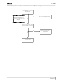
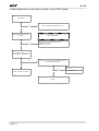
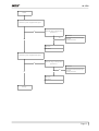
Service Manual
17-inch LCD Monitor
AL1702
Service Manual Versions and Revision
N o.
Ve rs ion
R e le as e D ate
R e vis ion
1.
1.0
May 12, 2004
O riginal release
Copyright
Trademarks
Copyright 2004 LiteOn Technology Corp.
LiteOn is a registered trademark of LiteOn
Technology Corp.
All Rights Reserved
This manual may not, in whole or in part, be
copied, photocopied, reproduced, translated, or
converted to any electronic or machine readable
form without prior written permission of LiteOn
Technology Corp.
ACER AL1702 Service Manual.
Printed in Taiwan.
All other trademarks are the property of their
respective owners.
AL1702
1) Circuit Description
1.
Power Board Operation Therory -------------------------------------------------------------------------------------------- 3
2.
Inverter -------------------------------------------------------------------------------------------------------------------------- 4
3.
Interface ------------------------------------------------------------------------------------------------------------------------- 5
3.1 Top --------------------------------------------------------------------------------------------------------------------------- 5
3.2 Power ------------------------------------------------------------------------------------------------------------------------ 5
3.3 VGA & DDC interface ----------------------------------------------------------------------------------------------------- 5
3.4 Scaler MST8111A --------------------------------------------------------------------------------------------------------- 5
3.5 Panel interface -------------------------------------------------------------------------------------------------------------- 5
3.6 Audio ------------------------------------------------------------------------------------------------------------------------ 7
4.
Others --------------------------------------------------------------------------------------------------------------------------- 7
4.1 Detection of POWER switch status ------------------------------------------------------------------------------------ 7
4.2 Display mode identification ---------------------------------------------------------------------------------------------- 7
4.3 Power ON sequence ------------------------------------------------------------------------------------------------------ 8
4.4 Power OFF sequence ----------------------------------------------------------------------------------------------------- 8
4.5List of I/O Pin Assignments of the I307 -------------------------------------------------------------------------------- 9
2) Trouble Shooting
1.
No display of screen (Screen is black, color of LED is amber) -------------------------------------------------------- 11
2.
Nothing displays on screen (Screen is black, color of LED is green) ------------------------------------------------ 12
3.
Checking the back light unit ----------------------------------------------------------------------------------------------- 15
4.
Abnormal screen------------------------------------------------------------------------------------------------------------- 16
Page 1
AL1702
6.
Abnormal plug and play operation --------------------------------------------------------------------------------------- 18
7.
Checking the interface circuit of sync signal ---------------------------------------------------------------------------- 19
7.1 Checking the control circuit of horizontal sync pulse ------------------------------------------------------------- 19
7.2 Checking the control circuit of vertical sync pulse ---------------------------------------------------------------- 19
8
Checking the resolution change IC movement -------------------------------------------------------------------------- 20
9.
Checking the DC/DC converter circuit ----------------------------------------------------------------------------------- 21
10. Checking the Audio circuit [option] -------------------------------------------------------------------------------------- 22
11. Checking inverter board circuit -------------------------------------------------------------------------------------------- 23
12. Power board ------------------------------------------------------------------------------------------------------------------ 24
3) Spare Parts
Recommended Spare Parts List ------------------------------------------------------------------------------------------------- 25
Page 2
AL1702
1) Circuit Description
1.
Power Board Operation
1.1
Line filter consists of C801, T801, C802, C803, C804. It eliminates high frequency interference to meet EMI’s
requirement.
1.2
Rec & Filter
Bridge diode D801 converts AC source into pulsed DC. This pulsed DC is smoothed and filtered by C805.
R802 is an NTC ( negative thermal coefficient ) resistor, used to reduce inrush current to be within safe range.
1.3
Power transformer :
T802 converts energy for square wave from power source C805 to secondary side to generate +12V and +22V.
1.4
Output :
The square wave from T802 is rectified by D809, D811, then filtered by C822, C817 to generate +12V and +22V
respectively. I804 is the regulator for +5V output.
1.5
Driver :
Q803 drive T802 from PWM control of I801 for power converted.
1.6
FB :
Negative feedback CKT consists of photo coupler I802 and adjustable regulator I803. It can maintain output
voltages +22V and +12V at a stable level.
1.7
PWM :
1.7.1 Start : When power is turned on, Q801 conducts due to bias from C805 and R805,R803. C807 is charged a
16 volt and a starting current about 0.3mA to pin 7 of I801. I801 starts to oscillate and outputs a pulse
train through pin 6 to drive Q803.
1.7.2 OPP : When Q803 turns on, C805 supplies a linearly increasing triangle current through the primary
inductance of T802 to the driver Q803, once the peak value of this current multiplied by R811 exceeds1
volt, pulse train will be turn off immediately to protect Q803, T802 from being burned out.
1.7.3 Regulation : If output voltage +22V or 12V goes up, the R terminal of I803 gets more bias, accordingly
photo transistor and photo diode flows more current. The voltage of pin 2 of I801 goes up too, making
the pulse width of pin 6 of I801 to become narrower. So the output voltage +5V will be pulled down to a
stable value.
1.7.4 OVP : If +22V or 12V goes up too much, the induced voltage on pin 4 of T802 becomes large also.
Suppose that it is over 18 volts, ZD801 conducts, pin 3 of I801 is pulled up over 1 volt. The pulse train at
pin 6 of I801 goes down to zero, shutting Q803 off immediately.
1.7.5 SCP : If output terminal is short to ground, photo transistor does not conduct, hence Q806 does not
conduct either. Then oscillation of I801 is stop, shutting Q803 off immediately.
Power Board Block Diagram
Line
Filter
Rec. &
Filter
Power
Transformer
PWM
Driver
Outpur Rec. & Filter
FB
Page 3
AL1702
2.
Inverter Operation
This unit operates on an output voltage of 22V from power source.
2.1
VCC: When On/Off pin of P802 is high level input, Q106 turns on and provides +5VDC for I101 power supply.
2.2
Control IC: I101 (OZ960S)
2.2.1
Enable : When pin 3 of I101 is over 1.5V, I101 works. If it is under 1.5V, I101 turns off.
2.2.2
OSC: When I101 enabled, R108/C115 (pin 17/pin18 of I101) determine the operating frequency.
2.2.3
SST: C104 (pin 4 of I101) provides soft start function.
2.2.4
Ignition: R109 (pin 8 of I101) provides higher operating frequency for more striking voltage until regulation of feedback of lamp current. C103 (pin 1 of I101) determine the striking time.
2.2.5
Dimming control: The divided voltage of R106/R105/R104 control the duty pulse of burst-mode to drive
Q105 and perform a wide dimming control for the CCFL. The burst-mode frequency is determined by C116.
2.2.6
Regulation: Pin 9/pin 10 of I101 provide regulation of the CCFL current from feedback. The non-inverting
reference (pin 10 of I101) is at 1.25V nominal.
2.3
Protection: Open-lamp protection in the ignition period is provided through both pin1 and pin 2 of I101 to ensure
a rated voltage is achieved and a required timing is satisfied.
Removal of the CCFL during normal operation will trigger the current amplifier (pin 9/pin 10 of I101) output and
shuts off the inverter. This is latch function.
2.4
2.4.1
Output drivers: The configuration prevents any shoot-through issue associated with bridge-type power
conversion applications. Adjusting the overlap conduction between I102 P-MOSFET and I103 N-MOSFET,
I101 N-MOSFET and I103 P-MOSFET, the CCFL current regulation is achieved.
2.4.2
Full-bridge switching/Transformer: I102/I103 /C123/T101 compose full-bridge switching to convert DC
into AC for driver the CCFL.
2.5
Detection: C128/C129/C132/D115/D114/C118 detect the output voltage and ensure a rated voltage by pin2 of
I101.
2.6
Feedback: D116/D117/R120/D108/R116 sense the lamp current for negative feedback and regulation. The divided
voltage on R116 will be at 1.25V.
Inverter Circuit Block Diagram
VCC
Regulator
VDD
Control IC : OZ960
ON / OFF
Brightness
control
Page 4
U.V.P.
Enable
Output driver
OSC
Protection
SST
Ignition
Dimming
control
Regulation
Full-bridge switching
Transformer
Detection
Feed back
Lamp
AL1702
3.
Interface Operation
3.1
Top (Circuit diagrams MAIN PWB 2 of 8)
This page is function block. (1) power. (2) VGA & DDC interface. (3) scaler MST8111B. (4) panel interface. (5)
audio (option).
3.2
Power (Circuit diagrams MAIN PWB 3 of 8)
3.2.1
P301 connector
A 5V power supply for LCD module, MCU, logic. And a 12V power supply for audio function. It is
generated from the P301 connector.
3.2.2
I301 : 3-terminal regulator
A 2.5V power supply for scaler IC I305, it is generated from the 5V source.
3.2.3
I302 : 3-terminal regulator
A 3.3V power supply for scaler I305, it is generated from the 5V source.
3.2.4
Q303, I312 : ON/OFF control for LCD module power
ON/OFF control (PANELVCC_EN) is performed for power ON/OFF and also for the power saving
sequence.
3.2.5
R306 : ON/OFF control for LCD module back light power
ON/OFF control (BKLT_EN) is performed for black light power ON/OFF and also for the power saving
sequence.
3.2.6
Q301,Q302 : Adjust back light luminance for LCD module
It is adjusted back light luminance control (BKLT_ADJ) is performed for the back light luminance.
3.3
VGA & DDC interface (Circuit diagrams MAIN PWB 4 of 8)
The analog video signals input, the AC-coupled video signal video signal is used to clamp the black level at
0V. and H/V sync to sclaer, and DDC plug & play function.
3.3.1
P302 connector
The video input signals from the P302 connector.
3.3.2
I304DDC EEPROM
This IC is support DDC2B of the VESA standard, also plug and play for the PC host.
3.4
Scaler MST8111B (Circuit diagrams MAIN PWB 5 of 8)
The I305 is scaled converter LSI for the LCD monitor.
The analog R, G, B signal input entered from the video input circuit is converted into the digital data of video
signal through the incorporated A/D converter. Based on this conversion, this device performs interpolation
during pixel extension. These interpolation digital data are transformed to LVDS signal. The I305 source
voltage is 3.3V and 2.5V, the device clock frequency is 14.318 MHz. The device control signal is from MCU
through the 3-wire bus.
The I305 scaler has support OSD function.
3.5
Panel interface (Circuit diagrams MAIN PWB 6 of 8)
3.5.1
P305 connector
The P305 is LVDS bus, output to LCD module. The output voltage is 5 voltage.
3.5.2
MCU (Circuit diagrams MAIN PWB 7 of 8)
The I307 MCU is system processor. It can programmed scaler, control power save sequence for the
system, input keypad function, output LED, control audio function, and ISP / DDC2Bi function.
Page 5
AL1702
3.5.3
X302 crystal
The X302 crystal is 11.0592MHz, support the operated clock to the MCU.
3.5.4
Reset circuit
The C396, R379, D316 is support reset signal to the MCU, then MCU have output hardware reset signal
(HWRESET) to the scaler.
3.5.5
I308EEPROM
The I308 is 24LC16 EEPROM, the data transfer between I308 and MCU is effected through the IIC bus
SCL (pin14) and SDA (pin13) of MCU. The OSD related setting data, I305 control data and other service
data, to be stored in I308.
3.5.6
P308 connector
The P308 has support keypad function. Control is give effect to for the push switch to be used when
the user changes the parameters, in order to modify the respective setting values. Whether the switch
has been pressed is identified with the switch input level that is turned “L”.
Each switch input port is pulled up at outside of MCU. Related ports of I307 based on Table 1.
Each parameter is stored in the I308 EEPROM, the contents of which are updated as required.
The P308 have LED Green and Amber light, the LED Green signal pin 36 from I307 MCU, and the LED
Amber signal pin 37 from I307 MCU.
Table 1 Related ports of I307
3.5.7
Pin No.
Pin 3
Pin 2
I/O
I
I
Signal name
KEY_POWER
KEY_MENU
Function
Soft power switch input
Exit/Enter switch input
Pin 41
Pin 42
Pin 1
I
I
I
KEY_DOWN
KEY_MINUS
KEY_PLUS
↓ switch input
← switch input
→ switch input
Remarks
Power key
Enter / withdraw from
OSD
Down key
- / Mute key
+ / Auto key
Audio control function
The I307 MCU output signal control audio mute and power, the pin33 is mute signal, the pin32 is
controlled audio power signal.
3.5.8
Scaler programmed function
The I307 MCU is used DDR direct bus, between I305 MST8111B and MCU I307.
3.5.9
ISP and DDC2Bi function
The DDC2Bi is VESA standard for the host PC system, it can through DDC2Bi bus control LCD monitor.
The I309 will off DDC_CLK and DDC_DAT signal, when LCD monitor is no power.
Can use ISP function for firmware modification.
The pin29 is bus clock (DDC_CLK), the pin28 is bus data (DDC_DAT). It is same of the IIC data bus.
3.5.10 The power save sequence function
First disable I307 pin31 (BKLT_EN) from H to L of LCD module back light power, delay some time, then
disable I307 pin9 (PANELVCC_EN) from H to L of LCD module power, and disable I307 pin32
(AUDIO_EN) from H to L of audio power, and through 3-wire bus programmed I305 MST8111B to
power down mode.
Page 6
AL1702
3.6
Audio (Circuit diagrams MAIN PWB 8 of 8) [OPTION]
3.6.1
P309 connector
The audio signal input received from the audio input terminal P309 from the jack input of the jack
board, P309 is applied to amplifier I311 of pin4 (L-CH) and pin9 (R-CH) through the low-pass filter
consisting of R417, R418, C419 and C420.
3.6.2
P310 connector
The audio signal is output to the audio output terminal P310, and to the internal speaker system.
3.6.3
I310 MOSFET
I310 MOSFET (CEM9435A) is cut audio power (12V) for the power save sequence. The signal
(AUDIO_EN) is ON/OFF I310 MOSFET through the Q311 control.
3.6.4
I311 amplifier
The I311 TDA7496L is audio amplifier, I311 operated power voltage is 12V.
I311 pin4 and pin9 is audio input port.
I311 pin14 and pin17 is audio output port.
I311 pin 12 is mute input from I307 MCU. The pin 6 is audio volume from the I305 MST8111B.
4
Others
4.1
Detection of POWER switch status
The MCU identifies the ON status of the two power supplies. The identification is made when the
power supply is turn off. For example, if the power supply is turn off with the POWER switch, the
POWER switch must be turn on when active the power supply again. If the power supply is turned off
by pulling out the power cord, then this power supply can be turned on by connecting the power cord,
without pressing the POWER switch.
4.2
Display mode identification
4.2.1
Display mode identification
The display mode of input signal is identified based on Table 2.
When the mode has been identified through the measurement of horizontal and vertical frequencies,
the total number of lines is determined with a formula of “Horizontal frequency / Vertical frequency =
Total number of number of lines”. Final identification can be made by examining the coincidence of the
obtained figure with the number of lines for the mode identified from the frequency. The Distinction
Hsync and Vsync of each mode is shown in Table 3.
When the detected frequency if the sync signal has changed, the total number of lines should be
counted even through it is range identified frequency in the same mode.
4.2.2
Out of range
This out of range mode is assumed when the frequency out of the horizontal / vertical signal is as
specified below.
Vertical frequency : 56 ~ 76 Hz.
Horizontal frequency : 30 ~ 81.1KHz.
4.2.3
Power save mode
The power save mode is assumed when the horizontal / vertical signals are as specified below.
If there is no horizontal sync signal input.
If there is no vertical sync signal input.
If the horizontal sync signal is outside the measuring range of MST8111B.
If the vertical sync signal is outside the measuring range of MST8111B.
Page 7
AL1702
Table 2 video mode
Mode
1
2
3
4
5
6
7
8
9
10
11
12
13
14
15
16
17
Resolution
720x400 (70Hz)
640x480 (59.94Hz)
640x480 (66.67Hz)
640x480 (72Hz)
640x480 (75Hz)
800x600 (56.25Hz)
800x600 (60Hz)
800x600 (72Hz)
800x600 (75Hz)
832x624 (74.55Hz)
1024x768 (60Hz)
1024x768 (70Hz)
1024x768 (75Hz)
1152x864 (75Hz)
1280x960 (60Hz)
1280x1024 (60Hz)
1280x1024 (75Hz)
H-Freq
(KHz)
31.469
31.469
35
37.861
37.5
35.156
37.879
48.077
46.875
49.722
48.363
56.476
60.023
67.5
60
63.981
79.976
Band Width
(MHz)
28.322
25.175
30.24
31.5
31.5
36
40
50
49.5
57.28
65
75
78.75
108
108
108
135
Polarity
H
V
+
+
+
+
+
+
+
+
+
+
+
+
+
+
+
+
+
+
+
Table 3 the Hsync, Vsync distinction
Indication
resolution
720 x 400
640 x 480
800 x 600
832 x 624
1024 x 768
1152 x 864
1280 x 960
1280 x 1024
1280 x 1024
Page 8
Distinction Hsync
Distinction Vsync
30.5KHz≦fH≦32.5KHz
30.5KHz≦fH≦32.5KHz
34KHz≦fH≦36KHz
36.9KHz≦fH≦38.9KHz
36.5KHz≦fH≦38.5KHz
34.2KHz≦fH≦36.2KHz
36.9KHz≦fH≦38.9KHz
47.1KHz≦fH≦49.1KHz
45.9KHz≦fH≦47.9KHz
48.7KHz≦fH≦50.7KHz
47.4KHz≦fH≦49.4KHz
55.5KHz≦fH≦57.5KHz
59KHz≦fH≦61KHz
66.5KHz≦fH≦68.5KHz
59KHz≦fH≦61KHz
62.9KHz≦fH≦64.9KHz
79KHz≦fH≦81KHz
69Hz≦fV≦71Hz
59Hz≦fV≦61Hz
65.7Hz≦fV≦67.7Hz
71.8Hz≦fV≦73.8Hz
74Hz≦fV≦76Hz
55.3Hz≦fV≦57.3Hz
59.3Hz≦fV≦61.3Hz
71.2Hz≦fV≦73.2Hz
74Hz≦fV≦76Hz
73.5Hz≦fV≦75.5Hz
59Hz≦fV≦61Hz
69Hz≦fV≦71Hz
74Hz≦fV≦76Hz
74Hz≦fV≦76Hz
59Hz≦fV≦61Hz
59Hz≦fV≦61Hz
74Hz≦fV≦76Hz
The fixed
mode
1
2
3
4
5
6
7
8
9
10
11
12
13
14
15
16
17
AL1702
4.3
Power ON sequence
When the POWER switch is pressed, the POWER OFF signal is turned “H”. when this “H” potential is
detected, the CPU begins to establish the respective power supplies according to the sequence show below.
Power Switch
157 ms
LED_G (LED)
1.8 sec
PANELVCC_EN
(Panel VCC)
1.84 sec
PCLK/DATA
(LVDS bus)
2 sec
BKLT_EN
(Backlight Power)
2 sec
AUDIO_EN
(Audio VCC)
4.4
Power OFF sequence
When the POWER switch is pressed, while the power supply is ON, the POWER ON signal is turned “H”.
when this “H” potential is detected, the CPU begins to turn off the respective power supplies according to
sequence show below.
Power Switch
LED_G
(LED)
90 ms
PANELVCC_EN
(Panel VCC)
350 ms
PCLK/DATA
(LVDS bus)
BKLT_EN
(Backlight Power)
AUDIO_EN
(Audio VCC)
316ms
90 ms
1.55 sec
Page 9
AL1702
4.5
List of I/O Pin Assignments of the I307
Pin No.
Initial
Function
Setting
3
P5.0
KEY_POWER
H
ON/OFF monitor power
2
P5.1
KEY_MENU
H
OSD enter/exit enable
1
P5.2
KEY_PLUS
H
OSD right enable
42
P5.3
KEY_MINUS
H
OSD left enable
41
P5.4
KEY_DOWN
H
OSD down enable
38
P1.0
LED_G
H
LED green enable
37
P1.1
LED_A
H
LED amber enable
20
P1.2
SCL
H
Clock of 3-wire bus for scaler
21
P1.3
SDA
H
Data of 3-wire bus for scaler
22
P1.4
CSZ
H
Chip select of 3-wire bus for scaler
25
P1.5
HWRESET
H
Reset enable to scaler
29
P3.0
RXD
H
UART interface data IN
28
P3.1
TXD
H
UART interface data OUT
19
P3.2
INT
H
Interrupt signal from the scaler
13
P3.4
ISDA
H
EEPROM data bus
14
P3.5
ISCL
H
EEPROM clock bus
27
P6.0
DDC_WP
L
DDC EEPROM write protection
26
P6.1
VGA_DET
H
VGA cable connected
9
P6.3
PANELVCC_EN
L
Panel power enable
31
P6.5
BKLT_EN
L
Back light power enable
32
P6.6
AUDIO_EN
L
Audio power enable
33
P6.7
MUTE
L
Audio mute enable
Note : Other I/O pin assignments of the I305 MST8111B
73
PWM0 BKLT_ADJ
Backlight brightness control
74
PWM1 VOLUME
Audio volume control
Page 10
Port
Signal Name
AL1702
1. No display of screen (Screen is black, color of LED is amber)
Does OSM display when you push
PROCEED buttom.
When a sugnal isn't being inputed, it is
indicated with "VIDEO INPUT". it is
indicated with "OUT OIF RANGE" at the
time of the frequency that it can't be
distinguished.
No
Proceed "No OSM display" section.
Yes
Check if the sync signal from computer is
output and if the video cable is connected
normally.
NG
Input the sync signal of computer, or
change the cable.
OK
Proceed "checking the resolution change
IC movement" section.
Page 11
AL1702
2. Nothing displays on screen (Screen is black, color of LED is green)
Is backlight lit?
NG
Refer "Checking the backlight unit" section"
OK
Does computer output RGB video
signals?
Check the video cable for failure. Check the host for output
signal with all black only.
NG
OK
1)Change pattern of video signal output on the host.
2)Rsconnect the video cable.
3)Change the video cable.
Check OSM menu is display on screen
when you push the "PROCEED" key.
NG
OK
Check if the LCD video signal cable is connected between the
MAIN PWB and LCD module.
Failure Point
NG
OK
Proceed "Abnormal sreen" dection"
Next Page
Page 12
The cable is disconnected.
AL1702
Continue
Check the 3.3V power are supplied on I302, pin2, 4.
NG
Check if the voltage on I302 pin3 that is
power DC at 5V.
Failure Point
NG
OK
OK
1) Printed wire broke between P301 pin1,
2 and I302.
2) Check power board.
Failure Point
I302 is failure
Check the 2.5V power are supplied on I302, pin2, 4.
NG
Check if the voltage on I302 pin3 that is
power DC at 5V.
Failure Point
NG
OK
OK
1) Printed wire broke between P301 pin1,
2 and I302.
2) Check power board.
Failure Point
I302 is failure
Next Page
Page 13
AL1702
Continue
Check the 5V power are supplied on
P305 pin 1, 2, 3 (to the LCD panel)
NG
Check if theVoltage on I312 pin2 that is
DC power at 5V.
Failure Point
NG
OK
1) FB314 is open.
2) Printed wire broke between P305 pin1, 2, 3,
FB304, and P301 pin1, 2.
Check if the TTL level on I312 pin,1
that TTL level is low.
OK
NG
OK
Check the PANELVCC_EN signal of the
rectangle input Q303 pin2 at TTL high
level.
Failure Point
I312 is failure.
NG
OK
Failure Point
1) Prined wire broke between Q303 pin
3, R309, R308 and I312 pin1.
2) Q303 is failure.
Failure Point
Check the P305 all LVDS signals.
NG
OK
Failure Point
1) The LVDS cable broke between P305
and LCD module.
2) LCD module is failure.
Page 14
1) Printed wire broke between Q303 pin 2 and
I307 pin9.
2) I307 is failure.
Failure Point
1) Printed wire broke betweenP305 and
I305 LVDS signals.
2) I305 is failure.
AL1702
3. Checking the back light unit
Is +12V supplied to inverter PWB ? (by
the power board)
Failure Point
NG
OK
1) Inverter cable disconnection.
2) Power board failure.
Check the BKLT_EN signal of the
rectangle input P301 pin 6 at TTL high
level.
Failure Point
NG
OK
1) printed wire broke between P301 pin6,
R306 and I307pin 31.
2) I307 is failure.
Check the BKLT_ADJ signal of the input
P301 pin5 from I305 pin73 is a PWM
signal.
Failure Point
NG
OK
1) printed wire broke between P301 pin5,
Q301, Q302 and I305 pin73.
2) I305 is failure.
Failure Point
Back light unit of LCD module is failure.
Page 15
AL1702
4. Abnormal screen
Check the R, G, B video signal from computer
input on P302 of video connector.
NG
OK
Failure Point
1) No R, G, B video signals output from host
computer, check computer.
2) Video signal cable disconnection.
Check the R, G, B input video signals on I305
pin63, 60, 58 respectively that their level is 0.5
to 0.7Vp-p.
NG
OK
Check all LVDS signals being output to P305
from I305?
NG
OK
Prpcess "Checking the resolution change IC
movement" section.
Page 16
Failure Point
In the case of the Red signal. (A Green and
Blue signal is the same path, too.)
1)Printed wire broke between P302 pin 9 and
I305 pin63.
2) Video cable is failure.
3) R322 is short or open.
4) R318 is short or open.
5) C332 is short or open.
Failure Point
Printed wire broke between I305 and P305.
AL1702
5. Abnormal OSM display adjust problem
Check the input TTL level whether was changed when
pressed function keys on the P308 pin3, 4, 5, 6. (normal is
high level, when push buttom, generated low level plus)
NG
Failure Point
OK
1) Function key wire disconnection.
2) Function key wire is failure.
3) Function key board is failure.
Check the input TTL level whether was changed when
pressed function keys on the I307 pin1, 2, 41, 42. (normal
is high level, when push buttom, generated low level plus)
NG
OK
Failure Point
1) Printed wire broke between P308 pin3 and I307 pin41.
2) Printed wire broke between P308 pin4 and I307 pin2.
3) Printed wire broke between P308 pin5 and I307 pin1.
4) Printed wire broke between P308 pin6 and I307 pin42.
5) C404, C405, C406, C407 is short.
6) R367, R368, R369, R370 is short or open.
Failure Point
I307 is failure.
Page 17
AL1702
6. Abnormal plug and play operation
Confirm the host computersupplies DDC2 mode.
NG
OK
Failure Point
The host machine is not communicatiog in DDC2
mode.
Check the voltage on P302 pin13 that is power DC
5 V.
NG
OK
Failure Point
TheVideo cable is failure.
Check the voltage on I304 pin8 that is power DC 5
V.
NG
Failure Point
1) Printed wire broke between I304 pin8, D309,
D310 and P302 pin13.
2) D309 or D310 is failure.
3) D315 is failure.
OK
Check the voltage on P302 pin11, 12 that is serial
data / clock signal.
NG
Failure Point
OK
TheVideo cable is failure.
Check the output signal of serial data / clock on I304
pin5, 6.
OK
NG
Failure Point
I304 is failure.
Failure Point
1) Printed wire broke between I309 pin2, 3, I304
pin5, 6 and P302 pin11, 12.
2) I309 maybe failure.
3) R336, R337 is open.
4) C349, C350 is short.
Page 18
AL1702
7. Checking the interface circuit of sync signal
7.1 Checking the control circuit of horizontal sync pluse
Check the horizontal sync signal on P302 pin3 TTL
level.
Failure Point
NG
Video cable is failure.
OK
Check the horizontal sync signal on I305 pin37 TTL
level.
NG
OK
Failure Point
1) Printed wire broke between P302 pin3 and
I305 pin37.
2) FB313, R329 open.
3) R331, C346 short.
Failure Point
Process "Checking the resolution change IC
movement" section.
7.2 Checking the control circuit of vertical sync pluse
Check the horizontal sync signal on P302 pin2 TTL
level.
NG
OK
Failure Point
Video cable is failure.
Check the horizontal sync signal on I305 pin36 TTL
level.
NG
OK
Failure Point
Failure Point
1) Printed wire broke between P302 pin3 and
I305 pin36.
2) FB312, R328 open.
3) R330, C345 short.
Process "Checking the resolution change IC
movement" section.
Page 19
AL1702
8. Checking the resolution change IC movement
Check +3.3V supply on I305 pin11, 21, 84, 94, 104, 114, 126, 55,
65, 35, 45, 51, 53.
NG
Proceed " Checking the DC/DC converter circuit" section.
OK
Check +2.5V supply on I305 pin18, 87, 97, 117.
NG
Proceed " Checking the DC/DC converter circuit" section.
OK
Check X301 14.318MHz clock input to I305 pin33 and 34 at TTL
level.
Failure Point
NG
OK
1) Printed wire broke between X301 and I305 pin33, 34.
2) C371, C375 short or open.
3) X301 failure.
Check I305 pin32 HWRESET signal is low level at normal
operation.
Failure Point
NG
OK
1) Printed wire broke between I305 pin32 and I307 pin23.
2) R410, R380 open.
3) I307 failure.
Check I305 pin69, 70, 71 3-wire bus signal is (Same of the IIC
signal).
Failure Point
NG
OK
Failure Point
I305 failure.
Page 20
1) Printed wire broke between I305 pin69, 70, 71 and I307 pin20, 21,
22.
2) I307 failure.
AL1702
9. Checking the DC/DC converter circuit
Check the 5V is output from P301 pin1, 2
NG
OK
Failure Point
1) Power wire disconnection.
2) Power board is failure.
Check the 5V is input to I302 pin3.
NG
Failure Point
OK
1) Printed wire broke between P301 pin1. 2
and I302 pin3.
2) FB301, FB302 open.
Check the 3.3V is output from I302 pin2, 4.
Failure Point
NG
I302 is failure.
OK
Check the 5V is input to I301 pin3.
NG
Failure Point
OK
1) Printed wire broke between P301 pin1. 2
and I301 pin3.
2) FB301, FB302, FB305 open.
Check the 2.5V is output from I301 pin2, 4.
NG
OK
Failure Point
I301 is failure.
Failure Point
1) Printed wire broke between I301 pin2. 4, I302
pin2, 4 and I305 MST8111A power supply pin.
2) FB314, FB315, FB316, FB317, FB318, FB319
open.
Page 21
AL1702
10. Checking the Audio circuit [OPTION]
Check the Audio signal input to P309
NG
OK
Failure Point
1) Audio wire disconnection.
2) Audio Jack board failure.
Check the 12V is input to I310 pin5, 6, 7, 8.
Failure Point
NG
OK
1) Printed wire broke between P301 pin7. 8
and I310 pin1, 2, 3.
2) FB320 open.
3) Printed wire broke between I307 pin32 and
I310 pin4.
4) Q311 failure.
5) I310 failure.
Check the 12V is input to I311 pin15, 16.
Failure Point
NG
OK
1) Printed wire broke between I310 pin5, 6, 7,
8 and I311 pin15, 16.
2) L301 open.
3) C412 short.
Check the VOLUME PWM signal input to I311
pin6.
NG
OK
Failure Point
1) Printed wire broke between I305 pin74 and
I311 pin6.
2) C422 short.
3) I305 failure.
Check the MUTE signal is input to I311 pin12 at
high level.
Failure Point
NG
OK
1) Prined wire broke between I307 pin33 and
I311 pin12.
2) C414 short.
3) I307 failure.
Check the Audio output signal to Speaker.
Failure Point
NG
OK
Failure Point
I311 failure.
Page 22
1) Speaker failure.
2) Prined wire broke between I311 pin14, 17
and P310.
3) C415, C418 open or short.
AL1702
11. Checking inverter board circuit
Check C101 pin is around .
On/off pin of P802 is over 2V.
Brightness pin is between 0V and 3.5V.
OK
NG
It is not inverter problem.
Check pin 5 of I101 is 5V.
OK
NG
Check Q106, Q102 and repair them.
Check CN102, CN103 is connected
right.
NG
OK
Check CCFL and repair them.
Check pin 3 of I101 is over 2V.
OK
NG
Check R128 and repair it.
Check pin 18 of I101 is triangle
pulse.
OK
NG
Check C115, R108, I101 and repair
them.
Check pin 4 of I101 there is soft start
edge up to 4V and pin 11, 12, 19, 20
there is some pulse output.
OK
NG
Repair I101.
Check pin 2 of I101 there is below
2V from output detection.
OK
NG
Check C128/C129/C132/D115/
D114/C118 and repair them.
Check full-bridge (I102, I103, D102,
D103, C123) work right.
OK
NG
Repair them.
Check transformer (T101) work right.
and repair it.
Page 23
AL1702
12. Power Board
Check output voltage +5V, +12V and 22V
is right or not.
No
Yes
It is not power board problem.
Check power switch is turn on or not.
Yes
No
Turn switch on.
Check power cord (P801), signal
cable (P302), P802, P803, CN102,
CN103 is connected right or not.
No
Yes
Connect it right
Check C805 is about DC140V-330V
or not.
Yes
No
Check F801, D801, P801 and repair
them.
Check C807 is over 10V or not.
Yes
No
Check R805, R803, I801 and repair
them.
Check pin 6 of I801 have same
pulse or not.
Yes
No
Check peripheral co,of I801 and
repair them.
Check pin 1 of T802 have same
pulse or not.
Yes
No
Check Q803, R813, R814, D806,
R812 and repair them.
Check peak voltage of R811 triangle
pulse is up to 1 volt or not.
Yes
No
Check D804, R807 and repair them.
Check D809, D810, D811, C818,
C817, C822, T802 have same short
circuit, or the output +5V/+12V/+22V
is over load.
No
Yes
Check feedback circuit around I802,
I803 and the other components and
repair them.
Page 24
Repair them.
AL1702
3. Recommended Parts List
Note: 1.
If you have spare parts need, please check BOM to get the last release part number and
related information.
No.
Location
Part Number
Description
1
I301
6442036518
IC Linear AIC 1117-25CETR TO-252
2
I302
6442023326
IC Linear AIC 1084-33CM TO-263
3
I304
6448018208
IC 24LC02B SOP-8 MICROCHIP
4
I304
6448018218
IC M24C02 SOP-8 ST
5
I305
6444015206
IC MST8111B QFPQ-128 Mstar
6
I308
6448016508
IC 24LC16B SOP-8 MICROCHIP
7
I308
6448016518
IC M24C26 SOP-8 ST
8
I312
6444014708
FET P-Channel AO3401 SOT-23 AOS
9
I307
6448015578
IC MTV312MV64-AJ PLCC44 Myson
10
X301
6449006400
Crystal 14.318MHz AT-49 TOPICS
11
X302
6449004820
Crystal 11.0592MHz AT-49 TOPICS
12
I311
6442023100
IC Amplifier TDA7496L PDIP20 ST
13
L301
6111456131
Coil Choke 45uH DRWW 10x10
Page 25
2
3
4
5
6
7
8
9
10
11
12
13
14
15
REVISIONS
1
AUTH
1-1
A
ZONE
LTR
Carol
ECN
DESCRIPTION
A
DATE
APPROVED
RELEASE FOR PRELIMINARY
A
4
9
5
8
6-2
6-1
13
B
B
26
C
C
10
1-3
6-3
22
15
1-2
12
3
D
2
D
11
25
16
14
17
7
19
18
20
E
E
ITEM
1
SUB-ITEM
1-1
1-2
1-3
2
3
4
5
6
F
6-1
6-2
6-3
23
21-5
7
8
9
10
11
12
13
14
15
16
17
18
19
20
21
24
21-9
G
21-4
21-6
21-2
H
21-8
21-1
21-2
21-3
21-4
21-5
21-6
21-7
21-8
21-9
21-10
21-11
21-12
21-13
21-7
21-3
21-1
I
21-10
22
23
24
25
26
21-11
21-12
PART NO.
7737510250-0A
7742226850-0A
7742806820-0A
7742302330-0A
5113800138
7140130081
6814701400
7746501720-0A
7737807400-0A
7748708640-0A
7746501590-0A
7742002971-0A
7111230061-0A
5114300037
7111230061-0A
7116240081-0A
5113300481
7111230061-0A
7110430051
7748708650-0A
7130430061
7742404500-0A
7140330122-0A
7746203470-0A
7110430051
7742225150-0A
7737706850-0A
7742609580-0A
7742003070-0A
7742003060-0A
7748707730-0A
7742609570-0A
7742609560-0A
7112750581-0A
7385001501-0A
7742001150-0A
7742609590-0A
7140240201-0A
7740410053-0A
7742001030-0A
5114100017
7140840122-0A
7740201140-0A
6857104501
7141220061-0A
DESCRIPTION
F/C ASS'Y
FRONT COVER
PUSH BUTTON
LENS
PUSH BUTTON BD
SCREW M3x8L(BUTTON-BD)
QDI PANEL
BARRIER BOTTOM
QDI-CHASSIS ASS'Y
QDI CHASSIS BK
BARRIOER TOP
RUBBER
SCREW M3x6(I/F BD)
POWER BD
SCREW M3x6(PW BD)
SCREW M4x8(PW BD)
INTERFACE BD
SCREW M3x6(I/F BD)
SCREW M3x5(PANEL)
AC SUPPORT
SCREW M3x6(AC BK)
LOGO TYPE
SCREW M4x12(CHASSIS-F/C)
SHIELD
SCREW M3x5(CHASSIS-SHIELD)
REAR COVER
HINGE+BASE ASS'Y
AXIS STAND
WASHER-R
WASHER-L
AXIS-SUPPORT
AXIS-WHEEL-R
AXIS-WHEEL-L
SCREW M5x58(R-AXIS-L)
WASHER(AXIS)
NUT M5-7210050341(AXIS)
STAND-BLOCK
SCREW M4x14(STAND-BLOCK)
BASE
FOOT PAD
AUDIO BD
SCREW M4x12(FC-R/C)
SCREW M4x14-7110440142(R/C-AXIS)
SPEAKER
SCREW M2x6(SPEAKER)
Q'TY
1
1
1
1
1
3
1
1
1
1
1
2
2
1
3
1
1
4
4
1
2
1
2
1
1
1
1
1
1
1
1
1
1
1
1
1
1
3
1
6
F
G
H
2
2
1
4
J
SEE TABLE
MATERIAL:
LITE-ON TECHNOLOGY CO.
FINISH:
TITLE
PROCESS:
M17AAQ
USED ON:
21-13
DRAWN
DESIGN
K
DATE
Carol Huang
M17AAQ EXPLODE DWG
07/23'03
A1
CHECK
SCALE
APPROVE
1
2
3
4
5
6
7
8
9
10
11
12
13
K
DWG. NO.
PART NO.
1/1
SHEET
14
1
OF
1
15
5
4
3
2
1
ACER AL1502 / AL1702
D
D
SCHEMATIC REV 02 PTB-1468
27 April 2004
ROAD MAP
DESCRIPTION
C
SHEET NO.
TITLE SHEET
TOP
1
2
POWER
3
VGA & DDC INTERFACE
4
SCALER MST8111/6B
5
PANEL INTERFACE
6
AUDIO
7
C
REVISION HISTORY
REV.
DESCRIPTION
BASED ON SCHEMATICS FOR ACER
02
BY
LAST UPDATE
KT.LIN
27 April '04
B
B
A
A
Sheet:
LITE-ON TECHNOLOGY CO.
1
DRAWN:
Date:
DESIGN:
Date:
Title:
CHECK:
Date:
CHECK:
Date:
DWG.NO:
APPRO:
Date:
APPRO:
Date:
PCB. NO:
of
8
Size:
Custom
M15_17AAX
TITLE SHEET
8814680000-02
6832146800-02
5
4
3
2
1
5
4
3
2
1
D
D
B1
B2
RIN
GNDR
GIN
GNDG
SOG
BIN
GNDB
HSYNC
VSYNC
VCC5V
VCC5V
DDC5V
DDC_WP
RIN
GNDR
GIN
GNDG
SOG
BIN
GNDB
HSYNC
VSYNC
RIN
GNDR
GIN
GNDG
SOG
BIN
GNDB
HSYNC
VSYNC
VCC2V5
VCC3V3
DDC5V
DDC_WP
VCC2V5
VCC3V3
DDC_DAT
DDC_CLK
DDC_DAT
DDC_CLK
VGA_DET
VGA_DET
3.VGA & DDC INTERFACE
B3
C
VCC5V
VGA_DET
DDC_CLK
DDC_DAT
DDC_WP
DDC5V
C
VGA_DET
DDC_CLK
DDC_DAT
DDC_WP
DDC5V
ALE
RDZ
WRZ
HWRESET
INT
VCC5V
AD0
AD1
MUTE
AD2
AUDIO_EN
AD3
MUTE
AUDIO_EN
ALE
RDZ
WRZ
HWRESET
INT
AD0
AD1
AD2
AD3
PA[0..7]
PANELVCC_EN
BKLT_EN
PANEL12V_EN
PANELVCC_EN
BKLT_EN
PANEL12V_EN
PA[8..13]
IVCOM
VCC3V3
ALE
RDZ
WRZ
HWRESET
INT
AD0
AD1
AD2
AD3
PA[14..19]
IVCOM
6.MCU
VCC2V5
PB[0..5]
B4
PANEL12V_EN
BKLT_EN
PANELVCC_EN
PB[6..11]
PANEL12V_EN
BKLT_EN
PANELVCC_EN
PB[12..23]
GPO[0..4]
VLCD12V
VCC3V3
VCC2V5
B
ESP
OSP
VLCD
VCC5V
VDD15V
VCC5V
VDD15V
VLCD12V
VLCD
BKLT_ADJ
B5
PA[0..7]
PA[0..7]
PA[8..13]
PA[8..13]
PA[14..19]
PA[14..19]
PB[0..5]
PB[0..5]
PB[6..11]
PB[6..11]
PB[12..23]
GPO[0..4]
VLCD
GPO[0..4]
B
ESP
OSP
ESP
OSP
VLCD12V
VLCD
IVCOM
BKLT_ADJ
VLCD12V
PB[12..23]
IVCOM
BKLT_ADJ
5.PANEL INTERFACE
DGND
2.POWER
B6
AUDIO_EN
MUTE
VCC5V
AUDIO_EN
MUTE
VOLUME
VOLUME
VOLUME
VDD15V
VCC5V
VDD15V
DGND
7.AUDIO
4.SCALER MST8111/6B
A
A
Sheet:
LITE-ON TECHNOLOGY CO.
2
DRAWN:
Date:
DESIGN:
Date:
Title:
CHECK:
Date:
CHECK:
Date:
DWG.NO:
APPRO:
Date:
APPRO:
Date:
PCB. NO:
of
8
Size:
Custom
M15_17AAX
TOP
8814680000-02
6832146800-02
5
4
3
2
1
5
4
3
2
1
VCC5V
TO-252
R301
VCC5V
R302
I301
3
C
P301
VCC5V
PBY201209T-121Y-S
PBY201209T-121Y-S
VCC5V
3,6,7
4K7
3
FB301
FB302
1
2
3
4
5
6
7
8
9
10
B
Q301
MMBT3904
VDD15V
R305
0.1uF
2K2
1
C304
47uF/25V
1
Q302
MMBT3906
C306
R303
VOUT
2
ADJ
TAB
4
VCC2V5
C303
C305
47uF/25V
0.1uF(NC)
4
0.1uF(NC)
D
R304
2
3
VDD15V
C302
VIN
AIC1117-25CE
VDD15V
JWT-A2001WV2-10
E
2
1
D
VCC2V5
100
VCC5V
BKLT_ADJ
10K
C307
C308
10nF
0.1uF
4
10K
7
C311
C310
C301
0.1uF
0.1uF
47uF/25V
R306
BKLT_EN
6
1K
DGND
C312
R307
1uF
10K(NC)
TO-263
3,4,5,6,7
VCC5V
VCC3V3
I302
3
C
C313
VCC3V3
FB303
VOUT
2
ADJ
TAB
4
VCC3V3
4
C
C314
C316
47uF/25V
0.1uF(NC)
AIC1084-33CM
47uF/25V
G
NOTE: FOR PANEL POWER SELECTION.
IF 3.3V INSTALL FB303
IF 5V INSTALL FB304
1
C315
D
VCC5V
VIN
0.1uF(NC)
S
FB304
PBY201209T-121Y-S(NC)
PBY201209T-121Y-S(0ohm)
I312
AO3401
VLCD
FB306
2
C317
10K
VLCD
PBY201209T-121Y-S
5
C318
1
R308
3
680uF/10V
C323
C324
0.1uF
0.1uF
0.1uF(NC)
3
R309
R311
2
6 PANELVCC_EN
1K
Q303
MMBT3904
4K7
Note : If input power is +12V install R378.
C325
R378
VDD15V
1
0.1uF
0(NC)
B
B
FB305
TO-252
PBY201209T-121Y-S(NC)
VCC12V
I303
I313
AO3401(NC)
VCC12V
1
VLCD12V
FB307
FB308
2
PBY201209T-121Y-S(NC)
C327
100K(NC)
VLCD12V 5
PBY201209T-121Y-S(NC)
C320
VIN
VOUT
3
ADJ
TAB
4
C321
C322
47uF/25V(NC)
0.1uF(NC)
PJ78M12(NC)
47uF/25V(NC)
0.1uF(NC)
C326
1
R312
3
C319
2
47uF/25V(NC)
C329
C330
0.1uF(NC)
0.1uF(NC)
0.1uF(NC)
3
R313
R315
2
6 PANEL12V_EN
100K(NC)
Q305
MMBT3904(NC)
C328
0.1uF(NC)
1
4K7(NC)
A
A
Sheet:
LITE-ON TECHNOLOGY CO.
3
DRAWN:
Date:
DESIGN:
Date:
Title:
CHECK:
Date:
CHECK:
Date:
DWG.NO:
APPRO:
Date:
APPRO:
Date:
PCB. NO:
of
8
Size:
Custom
M15_17AAX
POWER
8814680000-02
6832146800-02
5
4
3
2
1
5
4
3
2
1
R317
VGA_DET 6
3
100
P302
VCC5V
2
VGA_CON
PC5V
SCL_VGA
SDA_VGA
14
13
12
11
10
9
8
7
6
5
4
3
2
1
1
D
FB309
D301
MMBD7000
R322
C336
75_1%
10pF(NC)
SBK160808T-300Y-S
C331
0.1uF
RED+
REDGREEN+
GREENBLUE+
BLUEHSYNC_IN
VSYNC_IN
FB310
R323
C337
75_1%
10pF(NC)
SBK160808T-300Y-S
R318
47
C332
47nF
R325
100
C339
47nF
R319
47
C333
47nF
R321
470
C335
1nF
R326
100
C340
47nF
R320
47
C334
47nF
R327
100
C341
47nF
D302
MMBD7000
D303
MMBD7000
4
GIN
4
SOG
4
GNDG
4
BIN
4
GNDB
4
D
SBK160808T-300Y-S
C343
0.1uF
R324
C338
75_1%
10pF(NC)
2
1
2
VCC5V
1
2
1
VCC5V
C342
0.1uF
GNDR
D304
MMBD7000
FB311
VCC5V
4
3
3
3
JWT-A2001WV2-14
RIN
C344
0.1uF
C
C
FB313
BK2125HS431
FB312
BK2125HS431
R329
330
R328
330
BEAD0805
BEAD0805
D307
D308
D305
MMSZ5232B
1N4148(NC)
MMSZ5232B
D306
1N4148(NC)
R330
R331
2K2
2K2
C345
C346
100pF
100pF
HSYNC
4
VSYNC
4
DDC5V
VCC5V
PC5V
DDC5V
B
C347
D309
0.1uF
1N4148
D310
1N4148
D315
C348
4K7
MMSZ5232B
0.1uF
3
R334
4K7
R336
R337
8
7
6
5
100
100
VCC
WP
SCL
SDA
A0
A1
A2
GND
1
2
3
4
R335
2
1
R333
10K
I304
SCL_VGA
SDA_VGA
B
R332
DDC5V
DDC_WP 6
Q306
MMBT3904
4K7
24C02
D311
D312
D313
C349
C350
47pF
47pF
D314
DDC_CLK
DDC_DAT
DDC_CLK 6
DDC_DAT 6
MMSZ5232B 1N4148(NC) MMSZ5232B 1N4148(NC)
A
A
Sheet:
LITE-ON TECHNOLOGY CO.
4
DRAWN:
Date:
DESIGN:
Date:
Title:
CHECK:
Date:
CHECK:
Date:
DWG.NO:
APPRO:
Date:
APPRO:
Date:
PCB. NO:
of
8
Size:
Custom
M15_17AAX
VGA & DDC INTERFACE
8814680000-02
6832146800-02
5
4
3
2
1
5
4
3
2
1
NOTE: IF IS 15" (XGA) PANEL, I305 IS SELECT MST8011B.
NOTE: IF IS 17" (SXGA) PANEL, I305 IS SELECT MST8111B.
VAD
VPLLVDVI VDPLL
VPO
VDD
VCC3V3
VPO
18
87
97
117
11
21
84
94
104
114
126
53
45
51
35
55
65
FB314
2
I305
MST8011B/8111B
VCC3V3
PBY160808T-600Y-S
C351
C353
C354
C355
C356
C357
C358
C359
10uF/16V
0.1uF
0.1uF
0.1uF
0.1uF
0.1uF
0.1uF
0.1uF
VCC2V5
VDD
C360
C361
C362
C363
C364
10uF/16V
0.1uF
0.1uF
0.1uF
0.1uF
63
62
60
59
61
58
57
37
38
29
28
R340
VDVI
40
41
43
44
46
47
49
50
52
RIN0
RIN0M
GIN0
GIN0M
SOGIN0
BIN0
BIN0M
HSYNC0
VSYNC0
DDC1_CLK/GPO8
DDC1_DAT/GPO7
VDDP
VDDP
VDDP
VDDP
VDDP
VDDP
VDDP
VDDC
VDDC
VDDC
VDDC
RIN
GNDR
GIN
GNDG
SOG
BIN
GNDB
HSYNC
VSYNC
RIN
GNDR
GIN
GNDG
SOG
BIN
GNDB
HSYNC
VSYNC
AVDD_PLL
3
3
3
3
3
3
3
3
3
AVDD_DVI
AVDD_DVI
AVDD
AVDD
D
AVDD_MPLL
D
R+
RG+
GB+
BCK+
CKREXT
390_1%
C
C368
0.1uF
VPO
R399
4K7
R400
6
ALE
6
RDZ
6
WRZ
6 HWRESET
6
INT
6
AD0
6
AD3
6
AD1
6
AD2
2
7
BKLT_ADJ
VOLUME
66
67
6
4K7(NC)
REFP
REFM
BUSTYPE
ALE
RDZ
WRZ
HWRESET
INT
AD0
AD3
AD1
AD2
69
71
70
32
72
30
31
77
78
ALE/CSZ
RDZ/SCL
WRZ/SDA
HWRESETZ
INT
AD0/GPO6
AD3/GPO5
AD1/EINV
AD2/OINV
BKLT_ADJ
VOLUME
73
74
PWM0
PWM1
33
XIN
C371 22pF
LVACKP/NC
LVACKM/NC
LVA2P/RA1P
LVA2M/RA1N
LVA1P/RA2P
LVA1MRA2N
LVA0P/RA3P
LVA0M/RA3N
106
107
108
109
110
111
112
113
PA0
PA1
PA2
PA3
PA4
PA5
PA6
PA7
NC/GA1P
NC/GA1N
NC/GA2P
NC/GA2N
LVA3P/GA3P
LVA3M/GA3N
98
99
100
101
102
103
PA8
PA9
PA10
PA11
PA12
PA13
NC/BA1P
NC/BA1N
NC/BA2P
NC/BA2N
NC/BA3P
NC/BA3N
88
89
90
91
92
93
PA14
PA15
PA16
PA17
PA18
PA19
NC/RB1P
NC/RB1N
NC/RB2P
NC/RB2N
NC/RB3P
NC/RB3N
16
17
22
23
24
25
PB0
PB1
PB2
PB3
PB4
PB5
NC/GB1P
NC/GB1N
NC/GB2P
NC/GB2N
NC/GB3P
NC/GB3N
8
9
12
13
14
15
PB6
PB7
PB8
PB9
PB10
PB11
118
119
120
121
122
123
124
125
128
1
4
5
PB12
PB13
PB14
PB15
PB16
PB17
PB18
PB19
PB20
PB21
PB22
PB23
LVB3P/CLKAP
LVB3M/CLKAN
LVBCKP/NC/CLKBP
LVBCKM/NC/CLKBN
LVB2P/NC/NC
LVB2M/NC/NC
LVB1P/NC/BB1P
LVB1M/NC/BB1N
LVB0P/NC/BB2P
LVB0M/NC/BB2N
NC/NC/BB3P
NC/NC/BB3N
B
FB315
2
P[0..7]
PA[8..13]
PA[14..19]
PA[0..7]
5
PA[8..13]
5
VCC2V5
PBY160808T-600Y-S
PA[14..19] 5
VCC3V3
NC/ESP
NC/OSP
75
76
ESP
OSP
GPO0
GPO1
GPO2
GPO3
GPO4
83
82
81
80
79
GPO0
GPO1
GPO2
GPO3
GPO4
PB[6..11]
PB[12..23]
ESP
OSP
PB[0..5]
5
PB[6..11]
5
ESP
OSP
C366
C367
10uF/16V
0.1uF
0.1uF
5
5
VCC3V3
GPO[0..4]
C365
PB[12..23] 5
VPLL
FB317
GPO[0..4] 5
PBY160808T-600Y-S
C369
C370
10uF/16V
0.1uF
B
VCC3V3
VDVI
GNDP
GNDP
GNDP
GNDP
GNDP
GNDP
GNDP
10
20
85
95
105
115
127
AVSS_PLL
AVSS_DVI
AVSS_DVI
AVSS_DVI
39
42
48
68
56
64
54
BYPASS
AVSS_LPLL
AVSS_MPLL
XOUT
AVSS
AVSS
AVSS
3
2
19 GNDC
86 GNDC
96 GNDC
116 GNDC
FB318
34
36
C376 0.1uF
C
PBY160808T-600Y-S
X301
14.318MHZ
C375 22pF
VAD
FB316
PB[0..5]
PBY160808T-600Y-S
MST8111/8031B
MST8116/8036B
VCC3V3
C372
C373
C374
10uF/16V
0.1uF
0.1uF
VDPLL
FB319
PBY160808T-600Y-S
C377
C378
10uF/16V
0.1uF
A
A
Sheet:
LITE-ON TECHNOLOGY CO.
5
DRAWN:
Date:
DESIGN:
Date:
Title:
CHECK:
Date:
CHECK:
Date:
DWG.NO:
APPRO:
Date:
APPRO:
Date:
PCB. NO:
of
8
Size:
Custom
M15_17AAX
SCALER MST8111/6B
8814680000-02
6832146800-02
5
4
3
2
1
5
4
PA[0..7]
4
PA[0..7]
4
4
PA[0..7]
PA[0..7]
PA2
PA3
PA4
PA5
PA6
PA7
D
3
4
PA0
PA1
PA2
PA3
PA4
PA5
PA6
PA7
PA12
PA13
RA1P
RA1N
RA2P
RA2N
RA3P
RA3N
LVACKP
LVACKM
LVA2P
LVA2M
LVA1P
LVA1M
LVA0P
LVA0M
LVA3P
LVA3M
4
PA8
PA9
PA10
PA11
PA12
PA13
GA1P
GA1N
GA2P
GA2N
GA3P
GA3N
PB0
PB1
PB2
PB3
PB4
PB5
RB1P
RB1N
RB2P
RB2N
RB3P
RB3N
PB6
PB7
PB8
PB9
PB10
PB11
GB1P
GB1N
GB2P
GB2N
GB3P
GB3N
P303
RA3N
RA3P
PB[6..11]
PB[6..11]
PB[12..23]
4 PB[12..23]
4
PA[14..19]
4
PA14
PA15
PA16
PA17
PA18
PA19
PB12
PB13
C
4
GPO[0..4]
PB18
PB19
PB20
PB21
PB22
PB23
PB[12..23]
PB[12..23]
PB12
PB13
PB14
PB15
PB16
PB17
PB18
PB19
PB20
PB21
BA1P
BA1N
BA2P
BA2N
BA3P
BA3N
CLKAP
CLKAN
LVB3P
LVB3M
LVBCKP
LVBCKM
LVB2P
LVB2M
LVB1P
LVB1M
LVB0P
LVB0M
4
OSP
4
ESP
OSP
ESP
R342
R345
GPO0
GPO1
GPO2
GPO3
GPO4
R344
R346
R347
R348
R349
GPOO0
GPOO1
GPOO2
GPOO3
GPOO4
0(NC)
0(NC)
0(NC)
0(NC)
0(NC)
2
BB1P
BB1N
BB2P
BB2N
BB3P
BB3N
RA2N
RA2P
FB1N
FB1P
FB2N
FB2P
GA3N
GA3P
FG0N
FG0P
GA2N
GA2P
FG1N
FG1P
GA1N
GA1P
FG2N
FG2P
CLKAN
CLKAP
FCLKN
FCLKP
BA3N
BA3P
FR0N
FR0P
BA2N
BA2P
FR1N
FR1P
BA1N
BA1P
FR2N
FR2P
GPOO1
GPOO0
STH
LP
POL
HMS
GPOO3
GPOO2
GPOO4
CLKV
STV
OE
0(NC)
C379
C381
10pF(NC)
10pF(NC)
R350
R351
R352
R353
R354
R355
R356
VLCD
VLCD
VLCD12V
2
32
31
50
49
48
47
46
45
44
43
42
41
40
39
38
37
36
35
34
33
32
31
30
29
28
27
26
25
24
23
22
21
20
19
18
17
16
15
14
13
12
11
10
9
8
7
6
5
4
3
2
1
FB0N
FB0P
RA1N
RA1P
0(NC)
GPO[0..4]
P304
52
51
PB14 CLKBP
PB15 CLKBN
PA[14..19]
1
PB[0..5]
PB[0..5]
PA[8..13]
PA[8..13]
2
0(NC)
0(NC)
0(NC)
0(NC)
0(NC)
0(NC)
0(NC)
RB2N B1N
RB2P B1P
RB1N B2N
RB1P B2P
GB3N BG0N
GB3P BG0P
GB2N BG1N
GB2P BG1P
GB1N BG2N
GB1P BG2P
CLKBNBCLKN
CLKBPBCLKP
BB3N BR0N
BB3P BR0P
BB2N BR1N
BB2P BR1P
BB1N BR2N
BB1P BR2P
C
AF730X-AXG1T(P-TWO)
FOR RSDS INTERFACE
VLCD
VLCD12V
C382 C383 C384 C385 C386
10pF(NC)
10pF(NC)
10pF(NC)
10pF(NC)
10pF(NC)
D
30
29
28
27
26
25
24
23
22
21
20
19
18
17
16
15
14
13
12
11
10
9
8
7
6
5
4
3
2
1
RB3N B0N
RB3P B0P
2
AF750X-AXG1T(P-TWO)
VLCD
FOR RSDS INTERFACE
P305
B
IVCOM( RSDS FOR LG )
VLCD
C
B
R357
E
1K(NC)
3
R358
R359
6
IVCOM
IVCOM
RXO3-
LVA3M
LVA2M
LVA1M
LVA0M
LVACKP
RXE3RXE2RXE1RXE0RXEC+
LVB2P
LVB1P
LVB0P
LVBCKP
RXO2+
RXO1+
RXO0+
RXOC+
1
3
5
7
9
11
13
15
17
19
21
23
25
27
29
31
R360
C387
C423
10K(NC)
22uF/16V(NC)
0.1uF(NC)
2
4
6
8
10
12
14
16
18
20
22
24
26
28
30
32
B
LVB3P
RXO3+
LVA3P RXE3+
LVA2P RXE2+
LVA1P RXE1+
LVA0P RXE0+
LVACKM RXECLVB2M RXO2LVB1M RXO1LVB0M RXO0LVBCKM RXOC-
CON32 (16X2)
0(NC)
Q307
MMBT3904(NC)
2
FOR LVDS INTERFACE
4K7(NC)
1
C388
LVB3M
Note: Pin5 and Pin 10 are no pin header
47pF(NC)
A
R350
AU 17
QDI 17
CPT 17
INNOLUX 15
HannStar 15
CPT 15
LG 15
NC
3.3V
0R
3.3V
0R
3.3V
0R
3.3V
0R
R351
NC
12V
0R
R352
R353
5V
0R
5V
0R
NC
3.3V
0R
3.3V
0R
3.3V
0R
NC
NC
NC
R354
R355
5V
0R
R356
NC
NC
NC
NC
NC
NC
NC
12V
0R
NC
NC
NC
NC
NC
NC
NC
0R
NC
A
R358
NC
12V
0R
NC
NC
12V
0R
Sheet:
LITE-ON TECHNOLOGY CO.
NC
6
DRAWN:
Date:
DESIGN:
Date:
Title:
CHECK:
Date:
CHECK:
Date:
DWG.NO:
APPRO:
Date:
APPRO:
Date:
PCB. NO:
of
8
Size:
Custom
M15_17AAX
PANEL INTERFACE
8814680000-02
6832146800-02
5
4
3
2
1
5
4
3
2
1
VCC5V
C394
D
C393
R365
R366
R367
R368
R369
R370
R371
0.1uF
4K7
4K7
4K7
4K7
4K7
4K7
4K7
10uF/16V
VCC5V
D
12
C398
R383
R381
11
C397 22pF
0.1uF
4K7
4K7
I308
1
2
3
4
A0
A1
A2
GND
VCC
WP
SCL
SDA
7
D316
R379
1N4148
10K
4
8
7
6
5
R382
R384
19
INT
100
100
C
14
13
27
26
16
9
30
31
32
33
DDC_WP
VGA_DET
PANEL12V_EN
PANELVCC_EN
IVCOM
BKLT_EN
AUDIO_EN
MUTE
3
DDC_WP
3
VGA_DET
2 PANEL12V_EN
2 PANELVCC_EN
5
IVCOM
2
BKLT_EN
7
AUDIO_EN
7
MUTE
24C16
P5.0
P5.1
P5.2
P5.3
P5.4
P5.5
X2
P5.6
RESET
DA8/HLFHO
DA9/HALFV
P1.0
P1.1
P1.2
INT0/P3.2
P1.3
P1.4
P1.5
ISCL/P3.5/T1
P1.6
ISDA/P3.4/T0
P6.0
P1.7
P6.1
DA7
P6.2
P4.0
P6.3
P4.1
P6.4
P4.2
P6.5
P6.6
P3.1/TXD
P6.7
P3.0/RXD
X1
VSS
X302
11.059MHZ
MTV312M64
VCC5V
R389
R390
R391
R385
4K7
4K7(NC)
4K7(NC)
4K7(NC)
3
2
1
42
41
40
34
39
38
17
18
20
21
22
23
24
25
35
36
37
15
KEY_POWER
KEY_MENU
KEY_PLUS
KEY_MINUS
KEY_DOWN
AD0
AD1
AD2
AD3
RDZ
WRZ
ALE
HW_RESET
R410
R393
R394
R397
R398
R372
R373
R374
R375
4K7
4K7
4K7
4K7
4K7(NC)
4K7
4K7
4K7
100
R380
LED_G
LED_A
AD0
AD1
AD2
AD3
RDZ
WRZ
ALE
HWRESET
100
AD0
4
AD1
4
AD2
4
AD3
4
RDZ
4
WRZ
4
ALE
4
HWRESET 4
C400
0.1uF
28
29
C
10
10uF/16V
NC
NC
VDD3
VCC
HSYNC
VSYNC
I307
C396
VCC5V
6
5
4
8
43
44
VCC5V
C395 22pF
VCC5V
DDC5V
C399
R386
R388
4K7
4K7
0.1uF
4K7
I309
8
7
6
5
VCC
OE2
1B
2B
0E1
1A
2A
VSS
VCC5V
1
2
3
4
DDC_DAT 3
DDC_CLK 3
3
R387
NC7WB3125
1
VCC5V
R392
2
Q308
MMBT3904
4K7
P307
1
2
3
4
JWT-A2001WV2-04(NC)
VCC5V
B
VCC5V
B
VCC5V
R376
3
LED_A
R377
4K7
Q309
MMBT3904
C352
1
2
3
4
5
6
7
8
9
KEY_DOWN
KEY_MENU
KEY_PLUS
KEY_MINUS
AMBER
GREEN
KEY_POWER
1
100
100
100
100
470
470
100
R402
LED_G
2
1uF
R403
R404
R405
R406
R407
R408
R409
4K7(NC)
3
1
2
P308
VCC5V
4K7(NC)
R401
4K7
Q310
MMBT3904
C380
1uF
JWT-A2001WV2-09
C401
C402
C403
C404
C405
C406
C407
0.1uF
0.1uF
0.1uF
0.1uF
0.1uF
0.1uF
0.1uF
A
A
Sheet:
LITE-ON TECHNOLOGY CO.
7
DRAWN:
Date:
DESIGN:
Date:
Title:
CHECK:
Date:
CHECK:
Date:
DWG.NO:
APPRO:
Date:
APPRO:
Date:
PCB. NO:
of
8
Size:
Custom
M15_17AAX
MCU
8814680000-02
6832146800-02
5
4
3
2
1
5
4
3
2
1
I310
CEM9435A
5
VDD15V
3
FB320
2
AUDIO_15V
VDD15V
6
AUDIO_15V
2
7
PBY201209T-300Y-S
D
C409
R411
C410
0.1uF
10K
100uF/25V
L301
1
8
D
45uH DRWW 10 X 10
FB321
R412
DGND
4
2,3,4,5,6
C411
PBY201209T-300Y-S
4K7
ANA-GND
0.1uF
VCC5V
R413
3
10K
R415
6
2
AUDIO_EN
VCC5V
2,3,6
ANA-GND
Q311
R414
MMBT3904
100K
4K7
1
R416
MUTE
6
10K
ANA-GND
C412
C413
C414
470uF/25V
0.1uF
0.1uF
C
C
ANA-GND
ANA-GND
R418
1K
IN_R
C416
2
1
9
1.0uF/50V
IN_L
C417
4
10
1.0uF/50V
JWT-A2001WV2-03
R419
R420
C419
C420
C421
47K
47K
47pF
47pF
100uF/25V
INL
SVR
C415
OUTR
14
STBY
MUTE
11
12
SP_R+
P310
470uF/25V
OUTL
1
2
3
4
C418
SP_L+
17
JWT-A2001WV2-04
470uF/25V
6
AUDIO IN
G2
G1
INR
VAO_L
AUDIO_IN_L
1K
5
R417
VOL
AUDIO_IN_R
1
2
3
G3
G4
G5
G6
G7
VAO_R
Vs
Vs
3
13
18
19
20
7
15
16
ANA-GND
P309
I311
TDA7496L
ANA-GND
FB322
ANA-GND
PBY201209T-300Y-S
ANA-GND
S-GND
ANA-GND
S-GND
B
B
4
R421
R422
62K
220K
C422
R423
0.1uF
VOLUME
180K
ANA-GND
A
A
Sheet:
LITE-ON TECHNOLOGY CO.
8
DRAWN:
Date:
DESIGN:
Date:
Title:
CHECK:
Date:
CHECK:
Date:
DWG.NO:
APPRO:
Date:
APPRO:
Date:
PCB. NO:
of
8
Size:
Custom
M15_17AAX
AUDIO
8814680000-02
6832146800-02
5
4
3
2
1
Printed in Taiwan