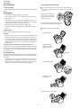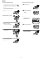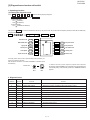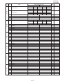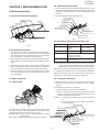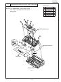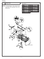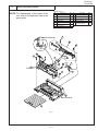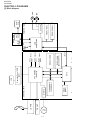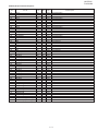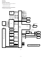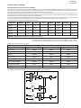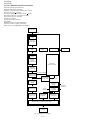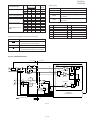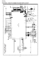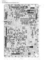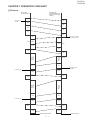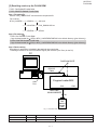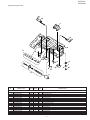
1
UX-B700U
FO-B1600U
SERVICE MANUAL
No. 00ZUXB700USME
FACSIMILE
MODEL
MODEL
UX-B700
FO-B1600
UX-B700
FO-B1600
SELECTION CODE DESTINATION
U
U.S.A.
Illustration: UX-B700U
CONTENTS
CHAPTER 1. GENERAL DESCRIPTION
[1] Specifications ............................................ 1-1
[2] Operation panel ......................................... 1-2
[3] Transmittable documents .......................... 1-3
[4] Installation ................................................. 1-4
[5] Quick setup guide ..................................... 1-9
[6] Quick reference guide ..............................1-10
CHAPTER 2. ADJUSTMENTS
[1] Adjustments ............................................... 2-1
[2] Diagnostics and service soft switch .......... 2-3
[3] Troubleshooting ....................................... 2-25
[4] Error code table ....................................... 2-26
CHAPTER 3. MECHANISM BLOCKS
[1] General description .................................. 3-1
[2] Ink jet printer ............................................ 3-3
[3] Disassembly and assembly
procedures ....................................... 3-6
CHAPTER 4. DIAGRAMS
[1] Block diagram ............................................4-1
[2] Wiring diagram .......................................... 4-2
[3] Point-to-point diagram ............................... 4-3
CHAPTER 5. CIRCUIT DESCRIPTION
[1] Circuit description ...................................... 5-1
[2] Circuit description of control PWB ..............5-2
[3] Circuit description of TEL/LIU PWB ........ 5-13
[4] Circuit description of printer PWB ............5-15
[5] Circuit description of
power supply PWB ............................5-18
[6] Circuit description of CIS unit ...................5-18
CHAPTER 6. CIRCUIT SCHEMATICS AND
PARTS LAYOUT
[1] Control PWB circuit ................................... 6-1
[2] TEL/LIU PWB circuit ............................... 6-10
[3] Printer PWB circuit ...................................6-14
[4] Power supply PWB circuit ...................... 6-20
[5] Operation panel PWB circuit ................... 6-22
[6] Ink PWB circuit ........................................ 6-24
CHAPTER 7. OPERATION FLOWCHART
[1] Protocol ..................................................... 7-1
[2] Power on sequence .................................. 7-2
CHAPTER 8. OTHERS
[1] Service tools .............................................. 8-1
[2] Changing the record paper size ................ 8-6
[3] Rewriting version up the FLASH ROM .......8-7
PARTS GUIDE
Parts marked with " " are important for maintaining the safety of the set. Be sure to replace these parts with specified ones for
maintaining the safety and performance of the set.
SHARP CORPORATION
This document has been published to be used
for after sales service only.
The contents are subject to change without notice.
UX-B700U
FO-B1600U
CAUTION FOR BATTERY REPLACEMENT
(Danish)
ADVARSEL !
Lithiumbatteri-Eksplosionsfare ved fejlagtig håndtering.
Udskiftning må kun ske med batteri af samme fabrikat og type.
Levér det brugte batteri tilbage til leverandoren.
(English)
Caution !
Danger of explosion if battery is incorrectly replaced.
Replace only with the same or equivalent type
recommended by the equipment manufacturer.
Discard used batteries according to manufacturer’s
instructions.
(Finnish)
VAROITUS
Paristo voi räjähtää, jos se on virheellisesti asennettu.
Vaihda paristo ainoastaan laitevalmistajan suosittelemaan
tyyppiin. Hävitä käytetty paristo valmistajan ohjeiden
mukaisesti.
(French)
ATTENTION
Il y a danger d’explosion s’ il y a remplacement incorrect
de la batterie. Remplacer uniquement avec une batterie du
même type ou d’un type recommandé par le constructeur.
Mettre au rébut les batteries usagées conformément aux
instructions du fabricant.
(Swedish)
VARNING
Explosionsfare vid felaktigt batteribyte.
Använd samma batterityp eller en ekvivalent
typ som rekommenderas av apparattillverkaren.
Kassera använt batteri enligt fabrikantens
instruktion.
(German)
Achtung
Explosionsgefahr bei Verwendung inkorrekter Batterien.
Als Ersatzbatterien dürfen nur Batterien vom gleichen Typ oder
vom Hersteller empfohlene Batterien verwendet werden.
Entsorgung der gebrauchten Batterien nur nach den vom
Hersteller angegebenen Anweisungen.
UX-B700U
FO-B1600U
CHAPTER 1. GENERAL DESCRIPTION
[1] Specifications
Automatic dialing:
Rapid Key Dialing: 18 numbers
Speed Dialing: 81 numbers
Print cartridge:
Initial cartridge
Approx. yield 300 letter pages
at 4% coverage*
Replacement cartridge: SHARP UX-C70B
Approx. yield 600 letter pages
at 4% coverage*
Memory size**:
1.8 MB (approx. 100 average pages)
Modem speed:
14,400 bps with auto fallback
to lower speeds.
Transmission time**:
Approx. 6 seconds (only when ECM is on)
Letter/A4: 20 pages max. (20-lb. paper)
Legal: 5 pages max.
Recording system:
Thermal inkjet
Halftone (grayscale):
Compatibility:
ITU-T (CCITT) G3 mode
Effective scanning width: 8.3" (210 mm) max.
Effective printing width:8.0" (203 mm) max.
600 x 600 dpi
Automatic document
feeder:
Letter: Approx. 200 sheets (20-lb. copier
paper at room temperature; maximum stack
height should not be higher than the line on
the tray)
Legal: 100 sheets
Recommended paper weight:
20-lb. Copy Bond
Input document size: Automatic feeding:
Width: 5.8 to 8.5" (148 to 216 mm)
Length (20 pages): 5.5 to 11" (140 to 279 mm)
Length (5 pages): 5.5 to 14" (140 to 356 mm)
Manual feeding:
Width: 5.8 to 8.5" (148 to 216 mm)
Length: 5.5 to 23.6" (140 to 600 mm)
Scanning Resolution: Horizontal:
203 lines/inch (8 lines/mm)
Vertical:
Standard: 98 lines/inch
(3.85 lines/mm)
Fine /Halftone: 196 lines/inch
(7.7 lines/mm)
Super fine: 391 lines/inch
(15.4 lines/mm)
Print resolution:
Paper tray capacity:
Contrast control:
Automatic/Dark selectable
Reception modes:
TEL/FAX/AM
Copy function:
Single/Multi/Sort (99 copies/page)
Telephone function:
Yes (cannot be used if power fails)
Applicable telephone Public switched telephone network
line:
64 levels
Display:
16-digit LCD display
Power requirements:
120 V AC, 60 Hz
Operating temperature: 60 - 90°F (15 - 32°C)
Compression scheme: MR, MH, MMR
* When Ink Save mode is enabled.
** Based on Sharp Standard No. 1 Chart at standard resolution,
excluding time for protocol signals (i.e., ITU-T phase C time only).
Humidity:
25 - 80% RH
Power consumption:
Standby: 5.0 W
Maximum: 30 W
Dimensions (without
attachments):
Width: 14.6" (372 mm)
Depth: 10.2" (259 mm)
Height: 8.0" (203 mm)
Weight (without
attachments):
Approx. 11 lbs. (5.0 kg)
As a part of our policy of continuous improvement, SHARP reserves the right to make design and specification changes for product
improvement without prior notice. The performance specification figures indicated are nominal values of production units. There may be some
deviation from these values in individual units.
1–1
UX-B700U
FO-B1600U
[2] Operation panel
2 3
1
4
PLAIN PAPER INKJET FAX
TEL
ABC
1
GHI
03
04
05
06
AM
07
08
09
10
11
12
13
14
15
17/G1
18/G2
UP
FUNCTION
6
COPY/HELP
SPEED DIAL
WXYZ
8
16/POLL
RESOLUTION/
RECEPTION MODE
3
5
TUV
7
02
MNO
JKL
PQRS
01
DEF
2
4
FAX
9
Z
START/
MEMORY
A
REDIAL
HOLD
0
DOWN
SPEAKER
STOP
PANEL RELEASE
5
6 7
8
9
10
11 12
13
Illustration: UX-B700U
8. HOLD key
Press this key to put the other party on hold during a phone
conversation.When this is done, they cannot hear you. You
can put the handset back in the cradle without breaking the
connection. When you are ready to speak with the other
party again, pick up the handset. If you did not put the
handset back in the cradle, press the HOLD key again to
resume conversation.
9. PANEL RELEASE
Grasp here and pull up to open the operation panel.
10.COPY/HELP key
When a document is in the feeder, press this key to make a
copy of a document. At any other time, press this key to
print out the Help List, a quick reference guide to the
operation of your fax machine.
11.STOP key
Press this key to cancel an operation before it is completed.
12.START/MEMORY key
Press this key after dialing to begin fax transmission. Press
this key before dialing to send a fax through memory. The
key can also be pressed in the date and time display to
show the percentage of memory currently used.
13.Arrow keys
Use these keys to scroll through and select settings, and to
search for auto-dial numbers.
1. Display
This displays messages and prompts to help you operate
the machine.
2. FUNCTION key
Press this key followed by the arrow keys to select special
functions and settings.
3. RESOLUTION / RECEPTION MODE key
When a document is in the feeder, press this key to adjust
the resolution for faxing or copying. At any other time,
press this key to select the reception mode (an arrow in
the display will point to the currently selected reception
mode).
4. Rapid Dial Keys
Press one of these keys to dial a fax number automatically.
5. Number keys
Use these keys to dial numbers, and enter numbers and
letters when storing auto-dial numbers.
6. SPEED DIAL key
Press this key to dial a fax or voice number using an
abbreviated 2-digit Speed Dial number.
7. SPEAKER key
Press this key to listen to the line and fax tones through
the speaker when faxing a document.
Note: This is not a speakerphone. You must pick up the
handset to talk with the other party.
1–2
UX-B700U
FO-B1600U
[3] Transmittable documents
5. Automatic Document Feeder Capacity
1. Document Sizes
Number of pages that can be placed into the feeder at anytime is as
follows:
Normal size
width
length
Normal size: max. ADF 20 pages
5.8" - 8.5" (148 – 216 mm)
5.5" - 11" (140 – 279 mm)
Special size: Single sheet only (manual feeding)
NOTES:
(Max.)
(Max.)
Letter
size
(Min.)
•
600mm
279mm
216mm
[Normal size]
When you need to send or copy more pages than the feeder
limit, place additional pages in feeder when last page in
feeder is being scanned.
Place additional pages carefully and gently in feeder.
If force is used, double-feeding or a document jam may
result.
6. Readable Width & Length
140mm
148mm
•
The readable width and length of a document are slightly smaller than
the actual document size.
216mm
[Special size]
Note that characters or graphics outside the effective document scanning range will not be read.
Use document carrier sheet for smaller documents.
•
* With special sizes, only one sheet can be fed into the machine at a
time. Insert next page into feeder as current page is being scanned.
Readable width
8.3" (210mm), max.
2. Paper Thickness & Weight
20 sheets
1sheet(Manual)
70 kg
70 kg ~ 135 kg
21.5 lbs.
14 lbs. ~ 42 lbs.
(80 g/m2)
(52 g/m2 ~ 157g/m2)
Paper thickness (ref.) 0.1 mm
0.1 mm ~ 0.18mm
Paper size
LGL (216 mm x 355.6 mm)
A4 (210 mm x 297 mm)
LTR (216 mm x 279 mm)
Feeder capacity
A4/LTR: 20 sheets
LGL : 5 sheet
Paper weight
Readable width
3. Document Types
•
Normal paper
•
Documents handwritten in pencil (No. 2 lead or softer), fountain pen,
ball-point pen, or felt-tipped pen can be transmitted.
This is the length of the document sent minus 0.16" (4mm) from the top
and bottom edges.
Documents of normal contrast duplicated by a copying machine can
also be transmitted.
•
Diazo copy (blue print)
•
Carbon copy
Readable length
4mm
Diazo copy documents of a normal contrast may be transmitted.
Readable length
A carbon copy may be transmitted if its contrast is normal.
4mm
4. Cautions on Transmitting Documents
•
Documents written in yellow, greenish yellow, or light blue ink cannot
be transmitted.
•
Ink, glue, and correcting fluid on documents must be dry before the
documents can be transmitted.
•
All clips, staples and pins must be removed from documents before
transmission.
•
Patched (taped) documents should be copied first on a copier and
then the copies used for transmission.
•
All documents should be fanned before insertion into the feeder to
prevent possible double feeds.
1–3
UX-B700U
FO-B1600U
[4] Installation
2. Assembly and connections
1. Site selection
1 Connect the handset as shown and place it on the handset rest.
The ends of the handset cord are identical, so they will go into
either jack.
Take the following points into consideration when selecting a site for this
model.
ENVIRONMENT
•
•
The machine must be installed on a level surface.
•
Provide easy access to the front, back, and sides of the machine. In
particular, keep the area in front of the machine clear, or the original
document may jam as it comes out after scanning.
•
•
Make sure the handset cord
goes into the jack marked
with a handset symbol on the
side of the machine!
Keep the machine away from air conditioners, heaters, direct sunlight, and dust.
Use the handset to make ordinary phone calls,
or to transmit and receive faxes manually.
The temperature should be between 41 - 95°F(5 - 35°C).
The humidity should be between 25% and 85% (without condensation).
2 Attach the paper tray and paper trays.
ELECTRICITY
AC 120V, 60Hz, grounded(3-prong) AC outlet is required.
Attach the paper tray.
Caution!
•
Connection to a power source other than that specified will cause
damage to the equipment and is not covered under the warranty.
•
If your area experiences a high incidence of lightning or power surges,
we recommend that you install a surge protector for the power and
telephone lines. Surge protectors can be purchased at most telephone
speciality stores.
Pull the paper plate
toward you and attach
the paper tray cover.
If the machine is moved from a cold to a warm place...
Condensation may form on the reading glass if machine is moved from
a cold to a warm place, this will prevent proper scanning of documents
for transmission. Turn on the power and wait approximately 2 hours before using machine.
TELEPHONE JACK
Paper plate
A standard RJ11C single-line wall telephone jack must be located near
the machine. This is the telephone jack commonly used in most homes
and offices.
•
Plugging the fax machine into a jack which is not RJ11C single-line
wall telephone jack may result in damage to the machine or your
telephone system. If you do not know what kind of jack you have, or
need to have one installed, contact the telephone company.
Attach the document tray.
2
1
Pull out the received
document tray.
Attach the document exit support.
1–4
UX-B700U
FO-B1600U
3. Installing the Print Cartridge
3 Plug the power cord into a 120 V, 60 Hz, grounded AC (3-prong)
outlet.
Caution:
•
Do not plug the power cord into any other kind of outlet. This will
damage the machine and is not covered under the warranty.
•
Make sure you have removed all of the packing tape before
plugging in the power cord. Plugging in the power cord without
doing so may damage the machine.
•
The machine does not have a power on/off switch, so the power
is turned on and off by simply plugging in or unplugging the power
cord.
•
The initial starter print cartridge included with your fax can print about
300 letter-size pages.
•
When replacing the print cartridge, use a SHARP UX-C70B cartridge.
One cartridge can print about 600 letter-size pages.
The above yields are at 4% coverage in INK SAVE mode.
•
Caution!
Do not open the print compartment cover of the machine while it is
printing. If opened while printing, printing will stop.
Note: Keep ink cartridges sealed in their packages until you are ready
to install them. The ink in a sealed cartridge is guaranteed for one
year. It is recommended that you do not use a cartridge that has been
left unused for a long time after opening, as the print quality may be
considerably degraded.
•
Make sure the power cord of the machine is plugged in and paper is
loaded before installing or replacing the print cartridge.
1
Open the operation panel.
“CHECK CARTRIDGE” normally
appears in the display the first
time you plug in the machine.
This message appears until you
install the print cartridge.
If PRINTER ERROR or PRINTER ERROR/CHECK PAPER
appears...
In the event that the display shows either of the above messages, you must clear the error before installing the print
cartridge. The error can usually be cleared by opening and
closing the print compartment cover (see Step 2), or if a paper
jam has occurred, by removing the paper jam.
Note: If your area experiences a high incidence of lightning or
power surges, we recommend that you install surge protectors for
the power and telephonelines. Surge protectors can be purchased
at most telephone specialty stores.
4 Insert one end of the line cord into the jack on the back of the machine marked TEL. LINE. Insert the other end into a standard (RJ11C)
single-line wall telephone jack.
2
Open the print compartment cover.
• Press as shown and pull the cover
toward you.
L.S
ET
TE
L.L
INE
3
Remove only the tape from the the new
cartridge.
• Important: Make sure you remove all
of the tape.
NO GOOD
• CAUTION! DO NOT touch the gold
Setting the dial mode
contact area of the cartridge.
The fax machine is set for tone dialing. If you are on a pulse dial line, you must
set the fax machine for pulse dialing. Press the panel keys as follows:
4
OPTION SETTING
Make sure the cartridge holder is
between the "CARTRIDGE EXCHANGE
AREA" arrows on the label, and then
pull the green lever and open the
cartridge holder cover.
DIAL MODE
• If you are replacing the cartridge,
Display:
1
Press
2
Press
FUNCTION
once and
once and
3
Press
4
Select the dial mode:
3 times.
4 times.
once.
remove the old cartridge. If you are
going to use the old cartridge again,
place it in an air-tight container.
1=TONE, 2=PULSE
• CAUTION! DO NOT touch the contact
TONE:
5
Press
1
STOP
PULSE:
area inside the carriage carrier.
The display briefly shows
your selection, then:
2
QUIET TIME
Note: If the print compartment cover is left
open for approximately 30 minutes with a
cartridge installed, the cartridge will
automatically return to its home position. To
make the cartridge return to the CARTRIDGE
EXCHANGE AREA when this has happened,
close the cover and then open it again.
to exit.
1–5
NO GOOD
UX-B700U
FO-B1600U
5
Insert the new print cartridge into the
cartridge holder.
6
Place your index finger on the tab as
shown and close the cartridge holder
cover with your thumb. Make sure the
cover clicks into place.
7
Close the print compartment cover.
12
In the alignment page that the machine prints, locate the line that comes
closest to forming a completely straight line.
In this example, "15" comes
closest to forming a straight line.
13
8
1
5
• If you make a mistake, press
14
ENTER (0-30) 15
Press the number keys to enter the number of the straightest line.
Example:
Close the operation panel, pressing
down firmly on both front corners to
make sure it clicks into place.
After the alignment page is
printed, the display shows:
Press
START/
MEMORY
STOP
and then repeat the entry.
.
Display:
CHANGE CARTRIDGE
Note: If at any time the display shows the
alternating messages at right, check the printing
paper. If the tray is empty, add paper. If there is
paper in the tray, take it out and then reinsert it.
1=NEW, 2=OLD
9
When you are finished, press
Press
1 (NEW) if the cartridge you
installed is new.
Press
2
Display when "1" is selected:
NEW CART.: OK?
(OLD) if the cartridge you
installed is old.
OK: PRESS START
If you select the wrong number by mistake,
press
10
Press
STOP
and repeat the selection.
START/
MEMORY
.
If you selected "OLD" in the previous
step, this completes the installation
procedure. (Note: If you find that print
quality is not satisfactory after
reinstalling the old cartridge, align the
cartridge .)
Display when "NEW" is
selected:
ALIGN CARTRIDGE
If you selected "NEW", the display will
show the alternating messages at
right. Continue with the following steps
to align the print cartridge.
11
Press
1
1=PRINT,2=SET
to print an alignment page. (To enter an alignment value
without printing an alignment page, press
2 .)
1–6
START/
MEMORY
ADD PAPER &
PRESS START KEY
.
UX-B700U
FO-B1600U
4. Loading printing paper
1 Setting the paper size
You can load letter or legal size paper in the paper tray. Recommended paper
weight is 20-lb. Copy Bond. The maximum number of sheets is as follows:
Letter size:
Legal size:
1
2
The fax has been set at the factory to scale received faxes to letter size paper.
If you loaded legal paper, you must change the paper size setting to LEGAL.
Approx. 200 sheets (20-Ib. copier paper at room temperature;
maximum stack height should not exceed line on tray)
Approx. 100 sheets (20-Ib. copier paper at room temperature)
Pull the paper plate toward you, and
remove the paper tray cover from the
paper tray.
1
Press
2
Press
once and
3
Press
once.
4
Select the paper size:
If you are going to load legal paper, flip
up the paper tray extension.
5
3
FUNCTION
once and
twice.
Display:
PAPER SIZE SET
once.
1=LETTER,2=LEGAL
LEGAL:
The display briefly shows
your selection, then:
COPY CUT-OFF
LETTER:
1
Press
to return to the date and time display.
STOP
PRINT SET-UP
2
2 Contrast settings
Pull the paper plate toward you and insert the stack of paper into the
tray, PRINT SIDE UP.
AUTO
DARK
• If paper remains in the tray, take it out and combine it into a single stack
Use AUTO for normal documents.
Use DARK for faint documents.
with the new paper.
1
The stack
should not
be higher
than this line
• The document must be loaded before
the resolution and contrast can be
adjusted.
Be sure to load the paper so that
printing takes place on the print side
of the paper. Printing on the reverse
side may result in poor print quality.
4
Load the document(s).
2
Pull the paper plate toward you and
replace the paper tray cover.
Press
RESOLUTION/
RECEPTION MODE
one or more times
STANDARD
:AUTO
• The first time you move through the list
FINE
:AUTO
of resolution settings, the contrast
setting AUTO will appear next to each
resolution setting. The second time you
move through the list, the contrast
setting DARK will appear.
LETTER Place the
LEGAL cover using the
appropriate
notch for the
size of paper
loaded
Display:
until the desired resolution and
contrast settings appear in the display.
SUPER FINE :AUTO
HALF TONE
:AUTO
STANDARD
:DARK
FINE
:DARK
SUPER FINE :DARK
HALF TONE
:DARK
Note: In order to transmit in SUPER FINE resolution, the receiving fax machine
must also have that resolution. If it doesn't, your machine will automatically step
down to the next best available setting.
1–7
UX-B700U
FO-B1600U
5. Clearing a jammed document
6. Clearing jammed printing paper
If the original document doesn't feed properly during transmission or copying,
or DOCUMENT JAMMED appears in the display, first try pressing
the document doesn't feed out, remove it as explained below.
START/
MEMORY
1
Open the operation panel.
2
Open the print compartment cover.
. If
Important:
Do not try to remove a jammed document without releasing it as explained
below. This may damage the feeder mechanism.
1
Slowly open the operation panel until it
is half open.
• Press as shown and pull the cover
toward you.
2
3
Flip up the green levers on each side of
the white roller.
5
Gently pull the jammed paper out of the
machine, making sure no torn pieces
of paper remain in the print
compartment or rollers.
4
Close the print compartment cover.
5
Close the operation panel, pressing
down firmly on both front corners to
make sure it clicks into place.
Gently remove the document.
• Be careful not to tear the document.
4
3
Flip down the green levers on each
side of the white roller.
Close the operation panel, pressing
down on both sides to make sure it
clicks into place.
1–8
UX-B700U
FO-B1600U
[5] Quick setup guide
1
3. Close the print
compartment cover.
2. Remove the packing tape.
1. Press as shown and
pull to open the print
compartment cover.
Note: To enter your name and fax number
and set the data and time so that they
appear at the top of each fax you send, see
pages 26-29 of your operation manual.
2
3
Attach the trays.
1. Connect the handset.
Pull the paper plate
toward you and attach
the paper tray cover.
Paper plate
2. Connect the phone line cord to the
TEL. LINE jack and a wall jack.
2
L.S
ET
TE
L.L
INE
1
4
5
The stack should
not be higher
than this line
Load paper.
Flip up if loading
legal paper
Plug the power cord into a
120-V grounded outlet.
Insert the paper
print side up.
Note: If you are loading legal paper, see
page 22 of the operation manual to
change the paper size setting to LEGAL.
6
Install the Print Cartridge.
1. Open the operation
panel.
2. Press as shown and pull to open
the print compartment cover.
3. Remove only the tape from the new
cartridge.
IMPORTANT: Make sure you remove
all of the tape.
4. Make sure the cartridge holder is between the
"CARTRIDGE EXCHANGE AREA" arrows on the label,
and then pull the green lever and open the cartridge
holder cover.
Caution! Do not touch
the gold contact area.
NO GOOD
5. Insert the new print cartridge
into the cartridge holder.
6. Place your index finger on the tab and close
the cartridge holder cover with your thumb.
7. Close the print compartment cover
and then the operation panel.
Display:
CHANGE CARTRIDGE
1=NEW, 2=OLD
8. a. Press 1
b. Press
to select NEW.
START/
MEMORY
ALIGN CARTRIDGE
9. In the alignment page that the machine
prints, locate the line that comes closest
to forming a completely straight line.
Enter the number of that line.
Example: 1
5
1=PRINT,2=SET
(If you make a mistake, press
c. Press 1 to print an alignment page.
STOP
and
then repeat the entry.)
1–9
10. Press
STOP
START/
MEMORY
to exit.
and then
UX-B700U
FO-B1600U
[6] Quick reference guide
Sending Faxes
Receiving Faxes
Place your document
(up to 20 pages) face
down in the document
feeder.
Press
RESOLUTION/
RECEPTION MODE
until the arrow in the
display points to the desired reception
mode.
TEL FAX
JAN-01 10:30
A.M.
RESOLUTION/
RECEPTION MODE
Normal Dialing
TEL FAX
JAN-01 10:30
A.M.
TEL FAX
1. Lift the handset or press
JAN-01 10:30
SPEAKER .
A.M.
FAX mode: The fax machine automatically
answers and receives faxes.
2. Dial the fax number.
3. Wait for the reception tone (if a person
answers, ask them to press their Start
key).
4. Press
START/
MEMORY
TEL mode: Answer all calls (even faxes)
by picking up the handset. To begin fax
reception, press
START/
MEMORY
.
.
A.M. mode: Select this mode when you
want to use an answering machine that is
connected to the fax.
Rapid Key Dialing
Press the appropriate Rapid Key.
Transmission will begin automatically.
Storing Auto Dial Numbers
Speed Dialing
1. Press
2. Enter the 2-digit Speed Dial number.
3. Press
FUNCTION
1. Press
SPEED DIAL .
once and
once.
2. Enter a 2-digit Speed Dial number (01 to
99; 01 to 18 for Rapid Key Dialing).
START/
MEMORY
3. Enter the fax number and press
START/
MEMORY
.
Search Dialing
4. Enter a name by pressing number keys.
1. Press
A
(To enter two letters in succession that
Z
or
REDIAL
until the desired
require the same key, press
destination appears in the display.
after
entering the first letter.)
2. Press
START/
MEMORY
Direct Keypad Dialing
1. Dial the fax number.
2. Press
G=
N=
A=
H=
O=
V=
B=
I =
P=
W=
SPACE =
.
C=
J=
Q=
X=
D=
K=
R=
Y=
E=
L=
S=
Z=
F=
M=
T=
START/
MEMORY
.
5. Press
1 – 10
U=
START/
MEMORY
and then
STOP
.
UX-B700U
FO-B1600U
CHAPTER 2. ADJUSTMENTS
[1] Adjustments
General
Since the following adjustments and settings are provided for this model,
make adjustments and/or setup as necessary.
1. Adjustments of output voltage (FACTORY ONLY)
1. Install the power supply unit in the machine.
2. Set the recording paper and document.
3. When the document is loaded, power is supplied to the output lines.
Confirm that outputs are within the limits below.
Output voltage settings
12
PANEL PWB
CNPN
1
8
1
CNPW
Output
+5V
+30V
Connector
No.
Voltage limits
4.75V ~ 5.25V
27.0V ~ 33.0V
POWER SUPPLY
PWB
1
2
CNPW
1
1
Pin No.
1
2
3
4
5
6
7
8
PRINTER PWB
+30V
+30V
MG
MG
DG
DG
+5V
+5V
12
12
Connector
No.
Connector
No.
CNLIUA
Pin No.
1
2
3
4
5
6
7
8
9
10
11
12
Connector
No.
CNPN
1
3
5
7
9
11
13
15
17
19
21
23
25
27
1
2
3
4
5
6
7
8
9
10
11
12
KEN4A
KEN3A
KEN2A
KEN1A
DG
+3.3V
E
SEN0
SEN1
SEN2
SEN3
SEN4
2–1
27
28
27
28
CNPRT
CONTROL PWB
CNPRINT
CNPRT
Pin No.
Pin No.
+24V
DG
MICMUTE
TELIN
TELMUTE
RXIN
TELOUT
TXOUT
CML
CI–
HS–
RHS–
12
1 1
CNPN 2
CNLIUA
CNLIUA
TEL/LIU PWB
8
1
CNPW
CNPRINT
+30V
+30V
+3.3VP
+3.3VP
PD0
PD1
PD2
PD3
PD4
PD5
PD6
PD7
nSTROBE
PRTRES
2
4
6
8
10
12
14
16
18
20
22
24
26
28
MG
MG
DG
DG
nACK
BUSY
PERROR
nFAULT
SELECT
nSELECTIN
nINIT
nAUTOFD
PIN
SN_Cover
UX-B700U
FO-B1600U
2. IC protectors replacement
4. Volume adjustment
ICPs (IC Protectors) are installed to protect the motor driver circuit.
ICPs protect various ICs and electronic circuits from an overcurrent condition.
You can adjust the volume of the speaker, handset, and ringer using the
UP and DOWN keys.
The location of ICPs are shown below:
1. Press the SPEAKER key.
CNPW
CNPRT CNPN
FU101
FU1
(1) Speaker
2. Press the UP or DOWN until the display shows the desired volume
level.
CNPRINT
PRINTER PWB
Display:
(TOP SIDE)
SPEAKER: HIGH
↔
CONTROL PWB
(BOTTOM SIDE)
SPEAKER: MIDDLE
• Press SPEAKER key again to
turn off the speaker.
↔
CNMT
FU100
SPEAKER: LOW
(2) Handset
(1) FU100 (QFS-L1026YCZZ) is installed in order to protect IC’s from
an over-current generated in the motor drive circuit. If FU100 is open,
replace it with a new one.
(2) FU101 (QFS-L2016XHZZ) is installed in order to protect IC’s from
an over-current generated in the LIU or CIS control circuit. If FU101
is open, replace it with a new one.
(3) FU1 (QFS-L1027YCZZ) is installed in order to protect IC’s from an
over-current generated in the motor drive circuit. If FU1 is open, replace it with a new one.
1. When talking through the handset, press UP or DOWN until the
display shows the desired volume level.
Display:
↔
RECEIVER: HIGH
↔
RECEIVER: MIDDLE
RECEIVER: LOW
• Note: The volume reverts to
MIDDLE each time you
replace the handset.
(3) Ringer
1. Press the UP or DOWN key. (Make sure SPEAKER key has not been
pressed, the handset is not lifted, and a document is not loaded in the
feeder.)
Display:
• The ringer will ring once at the
RINGER: HIGH
selected level.
3. Settings
↔
(1) Dial mode selector
DIAL mode (Soft Switch No. SW-B4 DATA No. 3)
RINGER: MIDDLE
RINGER: LOW
FUNCTION
DISPLAY:
OPTION SETTING
↔
KEY :
↔
(step 1) Select "OPTION SETTING".
NUMBER OF RING
RINGER OFF: OK?
(step 2) Select "DIAL MODE".
KEY:
Push until DIAL MODE
indicated because the number of
's changes by the model.
DISPLAY:
DIAL MODE
2. If you selected RINGER OFF: OK?, to turn off the ringer, press START/
MEMORY key.
is
1=TONE, 2=PULSE
(step 3) Select, using "1" or "2".
KEY:
1
DISPLAY:
TONE SELECTED
KEY:
2
DISPLAY:
PULSE SELECTED
(step 4) End, using the "STOP" key.
KEY:
STOP
2–2
UX-B700U
FO-B1600U
[2] Diagnostics and service soft switch
1. Operating procedure
(1) Entering the diagnostic mode
Press FUNC → 9 →
→ 8 → # → 7 , and the following display will appear.
or TA95
TA77
/ TA71
After 2 sec: DIAG MODE
contorol PWB ROM
TA77 (UX-B700U)
TA95 (FO-B1600U)
printer PWB ROM
TA71 (UX-B700U/FO-B1600U)
Then press the START key. Select the desired item with the up key or the down key or select with the rapid key. Enter the mode with the START key.
(Diag•specifications)
FUNC
9
8
7
TA77 or TA95 /TA71
DIAG MODE
START
Soft switch mode
START
Rapid1
ROM & RAM check
START
Rapid2
Rapid11
START
Entry data receive
Aging mode
START
Rapid3
Rapid10
START
Entry data send
Panel key test
START
Rapid4
Rapid9
START
Auto feeder mode
Check pattern
START
Rapid5
Rapid8
START
Shading mode
Signals send mode
START
Rapid6
Rapid7
START
Memory clear
If the diag mode cannot be set, repeat the diag mode operation, performing the following operation.
After the power is turned on and "WAIT A MOMENT" is indicated, press
the STOP key.
In relation with the process response (request from Production
Engineering) "WAIT A MOMENT" clock indication may appear depending
on STOP key timing. If the STOP key is held down, "MEMORY CLEAR?"
appears.
START/
MEMORY
"Power ON" +
STOP
KEY
START
KEY
2. Diagnostic items
ITEM No.
Rapid No.
Contents
Function
1
Rapid 1
SOFT SWITCH MODE
Soft switches are displayed and changed. List can be output.
2
Rapid 2
ROM & RAM CHECK
ROM is sum-checked, and RAM is matched. Result list is output.
3
Rapid 3
AGING MODE
10 sheets of check patterns are output every 5 minutes per sheet.
4
Rapid 4
PANEL KEY TEST
Panel keys are tested. Result list is output.
5
Rapid 5
CHECK PATTERN
Check pattern is output.
6
Rapid 6
SIGNALS SEND MODE
Various signals of FAX communication are output.
7
Rapid 7
MEMORY CLEAR
Back-up memory is cleared, and is set at delivery.
8
Rapid 8
SHADING MODE
Shading compensation is performed in this mode.
9
Rapid 9
AUTO FEEDER MODE
Insertion and discharge of document are tested.
10
Rapid 10
ENTRY DATA SEND
Registered content is sent.
11
Rapid 11
ENTRY DATA RECEIVE
Registered content is received, and its list is output.
2–3
UX-B700U
FO-B1600U
3. Diagnostic items description
3. 1. Soft switch mode
3. 6. Signals send mode
This mode is used to send various signals to the circuit during FAX communication. Every push of START key sends a signal in the following
sequence. Moreover, the signal sound is also output to the speaker when
the line monitor of the soft switch is on.
Used to change the soft switch settings.
The soft switch which is stored internally is set by using the keys.
The available soft switches are SW-A1 to SW-P7.
The content of soft switches is shown in Soft switch description.
The contents are set to factory default settings.
[1] No signals
3. 2. ROM & RAM check
ROM executes the sum check, and RAM executes the matching test.
The result will be notified with the number of short sounds of the buzzer
as well as by printing the ROM & RAM check list.
Number of short sounds of buzzer 0 → No error
1 → FAX engine ROM error
2 → Printer engine ROM error
3 → RAM error
(4Kbytes SRAM or 2Mbytes DRAM or Printer 512bytes NV-RAM)
[10] 4800BPS (V.27ter)
[4] 14400BPS (V.17)
[11] 2400BPS (V.27ter)
[5] 12000BPS (V.17)
[12] 300BPS (FLAG)
[6] 9600BPS (V.17)
[13] 2100Hz (CED)
[7] 7200BPS (V.17)
[14] 1100Hz (CNG)
3. 8. Shading mode
The mode is used for the shading com-pensation. For reading, set up
the special original paper. (Refer to page 8-6)
The compensation memorizes the reference data of white and black for
reading.
Moreover, the memorized data is not erased even if memory clear mode
is executed.
3. 4. Panel key test
This mode is used to check whether each key operates properly. Press
the key on the operation panel, and the key will be displayed on the
LCD. Therefore, press all keys. At this time, finally press the STOP key.
When the STOP key is pressed, the keys that are not judged as "pressed"
will be printed on the result list.
• LED part of the contact image sensor (CIS) is kept on during the term
from when "START" of the panel test mode to end with the STOP key.
3. 9. Auto feeder mode
In this mode, a document is inserted and discharged to check the auto
feed function.
3. 5. Check pattern
Check patterns are printed on one sheet.
Printing performance:The following 4 items are checked.
• Print area:Checks that the print area is reserved.
• Nozzles:When checking the nozzle, make sure at least 1 line is printed
in each block: all the blocks of horizontal black bars and the black line
patterns in B and C ( B :16 patterns, C :13 patterns).
(Note: If the nozzle A is not spraying properly, checking the area B
and C may be difficult (or may not be printed at all). In this case,
print again.
• Vertical align:Checks that the straight vertical line is drawn instead of
crooked line.
• Skew:Checks the skew of the recording paper.
5 Top margin
[9] 7200BPS (V.29)
[3] 12000BPS (V.33)
This mode is used to clear the backup memory and reset to the default
settings.
If any document is present, copying will be executed sheet by sheet. If
no document is present, the check pattern will be printed sheet by sheet.
This operation will be executed at a rate of one sheet per 5 minutes, and
will be ended at a total of 10 sheets.
4 Bottom skew
7 Bottom margin
[2] 14400BPS (V.33)
3. 7. Memory clear
3. 3. Aging mode
Detailed of check patterns
1 Top skew
2 Nozzle test
[8] 9600BPS (V.29)
After this mode is started, set a document, and the document feed will
be automatically tested.
3. 10. Entry data send
This mode is used to send the registered data to another machine and
make the other machine copy the registered content.
Before sending in this mode, it is necessary to set the other machine at
the entry data receive mode.
The following, information will be send to the remote machine:
1. Telephone list data
2. Sender register data
3. Optional setting data
3 Vertical lines
6 Left margin
6
4. Soft switch content
5. Junk fax number
1
6. Recording setting list data
5
3. 11. Entry data receive
In this mode, the registered data sent from the other machine is received and the received data is registered in the machine. When this mode
is used for receiving, the other machine must be in the entry data send
mode.
A
B
2
After receiving is completed, the following lists are printed.
C
1. Telephone list data
2. Sender register list (*)
3. Optional setting list (*)
3
4. Soft switch content
0 1 2 3 4 5 6 7 8 9 10 11 12 13 14 15 16 17 18 19 20 21 22 23 24 25 26 27 28 29 30
5. Junk fax number list (*)
6. Recording setting list data (*)
(*): Refer to SETUP LIST
7
4
2–4
UX-B700U
FO-B1600U
4. Entering the printer diagnostic mode
Press FUNC → 9 →
→ 8 → # → 6 , and the following display will appear.
PRINT DIAG MODE
Then press the START key. Select the desired item with the up key or the down key or select with the rapid key. Enter the mode with the START key.
(Diag•specifications)
FUNC
9
8
6
PRINT DIAG MODE
4% DATA PRINT AGING
START
Rapid1
ASF AGING
START
Rapid2
ASF SKEW CHECK AGING
START
Rapid3
CROSS PATTERN
START
Rapid4
INITIAL CARTRIDGE DATA SETTING
START
Rapid5
PRINTER DOWNLOAD
START
Rapid6
IJP LIST MODE
START
Rapid7
PRINTER ERROR CHECK MODE
START
Rapid8
START
If the diagnostic mode cannot be set, repeat the diagnostic mode operation, performing the following operation.
After the power is turned on and "WAIT A MOMENT" is indicated, press the STOP key.
In relation with the process response (request from Production
Engineering) "WAIT A MOMENT" clock indication may appear depending
on STOP key timing. If the STOP key is held down, "MEMORY CLEAR?"
appears.
START/
MEMORY
"Power ON" +
STOP
KEY
START
KEY
5. Printer diagnostic items
ITEM No.
Rapid No.
Contents
Function
1
Rapid 1
4% DATA PRINT AGING
4% of printing data continue to be printed.
2
Rapid 2
ASF AGING
The feed of the paper is continued.
3
Rapid 3
ASF SKEW CHECK AGING
The frame pattern continues to be printed to check the inclination performance.
4
Rapid 4
CROSS PATTERN
The image data of the cross pattern to be printed.
5
Rapid 5
INITIAL CARTRIDGE DATA SETTING
It makes the dot counter the setting for the initial cartridge.
6
Rapid 6
PRINTER DOWNLOAD
This mode rewrites the software of the printer engine.
7
Rapid 7
IJP LIST MODE
The maintenance data is printed.
8
Rapid 8
PRINTER ERROR CHECK MODE
The cause of “PRINTER ERROR” message is displayed.
6. Printer diagnostic items description
6. 1. 4% data print aging
6. 4. Cross pattern
This mode is the aging mode that prints the text pattern of 4%
This mode prints the test pattern that tests the performance of the printer.
6. 2. ASF aging (all white)
6. 5. Initial cartridge data setting
This mode is the aging mode that tests the performance of the ASF function. This mode makes the dot counter the setting for initial cartridge,
And this mode resets the following counter.
6. 3. ASF skew check aging
1. Replacement counter of the cartridge
This mode is the aging mode that tests the performance of the ASF function. 2. Paper jam counter
Detailed of check patterns
6. 6. Printer download
1. Top skew
2. Bottom skew
This mode rewrites the software of the printer engine.
3. Top margin
4. Bottom margin
2–5
UX-B700U
FO-B1600U
6. 7. IJP list mode
Maintenance data of the printer is output.
[Details of maintenance data]
Item
Dot counter
Page counter
Number of head cleaning (Wiping of cartridge)
Replacement counter of the cartridge
Jam counter
Clear timing
At the replacement cartidge
At the replacement cartidge
At the initial cartridge setting
At the initial cartridge setting
At the initial cartridge setting
Updata timing
After printing
After printing
At the maintenance
At the replacement of cartridge
At every paper jam
6. 8. Printer error check mode
The cause of “PRINTER ERROR” message is displayed.
[Details of Display]
Display
PRINTER ERR 01
PRINTER ERR 02
PRINTER ERR 03
PRINTER ERR 04
PRINTER ERR 05
PRINTER ERR 06
PRINTER ERR 07
PRINTER ERR 08
PRINTER ERR 09
PRINTER ERR 10
PRINTER ERR 11
PRINTER ERR 12
PRINTER ERR 13
PRINTER ERR 14
PRINTER ERR 15
Cause of “PRINTER ERROR” message
Power on reset response was not received from printer.
Printer interface ASIC data buffer was full and not resume for 180sec.
Carrier was not reached to cap position for 15sec after cover closed.
NPA command was not forwarded to printer for 5sec.
Printer interface ASIC command buffer error was occurred during NPA command forwarding.
NPA response was not received for 5sec.
Printer interface ASIC response buffer error was occurred during NPA response receiving.
ESC* command was not forwarded to printer for 5sec.
Printer interface ASIC command buffer error was occurred during ESC* command forwarding.
Print data transfer from Printer interface ASIC to printer was not completed for 180sec.
Last printed page was not exited for 60sec.
Carrier was not reached to cap position for 60sec after last printed page was exited.
Alignment pattern or Clean nozzles pattern printing was not completed for 60sec.
Printer interface ASIC print data bit error was occurred.
Printer interface ASIC print data DRAM writing error was occurred.
PRINTER ERR 21
PRINTER ERR 22
PRINTER ERR 23
PRINTER ERR 24
PRINTER ERR 25
PRINTER ERR 26
PRINTER ERR 27
Reserved
Reserved
Reserved
Carrier stall error
Printer PWB NVRAM error
Printer could not output print data.
Printer head short error
PRINTER ERR 31
PRINTER ERR 32
PRINTER ERR 33
PRINTER ERR 34
PRINTER ERR 35
PRINTER ERR 36
PRINTER ERR 37
PRINTER ERR 38
PRINTER ERR 39
PRINTER ERR 40
PRINTER ERR 41
Received NPA response was not for "Loop Back" command.
Received NPA response was not for "Register For DSA" command.
Received NPA response was not for "Print Head Information" command.
Received NPA response was not for "Set Alignment Data" command.
Received NPA response was not for "Get Printer Firmware Version" command.
Received NPA response was not for "Printer ROM & RAM Check" command.
Received NPA response was not for "Printer ROM Checksum" command.
Received NPA response was not for "Cartridge Initial" command.
Received NPA response was not for "Default Cartridge" command.
Received NPA response was not for "Reset Wipe Count" command.
Received NPA response was not for "Reset Page Count" command.
PRINTER ERR 51
PRINTER ERR 52
PRINTER ERR 53
Invalid command parameters was forwarded to printer.
No supported command was forwarded to printer.
Forwarded command was rejected by printer.
2–6
UX-B700U
FO-B1600U
7. How to make soft switch setting
To enter the soft switch mode, press the following key entries in sequence.
Press FUNCTION
DATA No.
9
8
7
START
START
1 2 3 4 5 6 7 8
S F T SW-A1 = 0 0 0 0 0 0 0 0
Press FUNCTION key.
S F T SW-A1 = 1 0 0 0 0 0 0 0
Press
key.
Press
key.
S F T SW-A1 = 1 0 0 0 0 0 0 0
S F T SW-A1 = 1 0 0 0 0 0 0 0
Bit1 - 8 are set.
S F T SW-A1 = 1 0 0 0 0 0 0 0
Press START key during setting.
S F T SW-A2 = 0 0 0 0 0 0 0 0
Soft SW-A2 - SW-P7 are set.
S F T SW-P7 = 0 0 0 0 0 0 0 0
To finish the settings halfway between
SW-A1 and SW-N3, press the STOP
key. In this case, the setting being done
to the SW No. on display will be nullified
while settings done to the preceding
SW No. remain in effect.
When the COPY key is pressed, the
contents of soft switches are printed.
The soft switch mode is terminated.
2–7
UX-B700U
FO-B1600U
8. Soft switch description
• Soft switch
SW
NO.
SW
l
A1
DATA
NO.
SW
l
A4
Initial
setting
0
Protect from echo
Forced 4800bps reception
Footer print
No
Yes
Yes
Yes
No
No
0
0
0
4
Length limitation of copy/send/receive
No limit
Copy/Send: 60 cm
Receive: 1 m
0
5
CSI transmission
Not transmitted
Transmitted
0
6
DIS receive acknowledgement during G3
transmission
Twice
NSF: Once
DIS: Twice
0
7
Non-modulated carrier for V29 transmission
mode
Yes
No
0
EOL (End Of Line) detect timer
25 s
13 s
0
Modem speed
SW
l
A3
1
1
2
3
8
SW
l
A2
Switch setting and function
ITEM
V.33
V.17
V.29
V.27 ter
14400 12000 14400 12000 9600 7200 9600 7200 4800 2400
1
0
0
1
1
1
1
0
0
0
0
1
2
3
1
0
1
1
0
0
0
1
0
0
0
1
0
0
0
1
0
1
0
0
0
0
0
0
0
0
1
1
1
1
0
0
4
Remarks
0
5
6
Sender’s information transmit
Reserved
No
Yes
0
0
7
Communication error treatment in RTN
sending mode (Reception)
No communication error
Communication error
0
8
CNG transmission
CED tone signal interval
No
1
No. 1
1000ms
1
2
No. 2
1
Yes
750ms
1
500ms
0
75ms
0
0
0
0
1
0
0
3
MR coding
No
Yes
0
4
5
6
ECM mode
ECM MMR mode
Reserved
No
No
Yes
Yes
0
0
0
7
8
Reserved
Reserved
1
2
3
4
Signal transmission level
0
0
Binary input
16 8 4 2 1
1 2 3 4 5
EX 0 1 0 0 0
0
1
0
0
No. =
5
eg. Signal transmission level is set to –8dBm.
0
6
Protocol monitor (Error print)
Printed at communication error
Not printed
0
7
8
Protocol monitor
Line monitor
Yes
Yes
No
No
0
0
2–8
OPTION
UX-B700U
FO-B1600U
SW
NO.
DATA
NO.
Switch setting and function
ITEM
1
Digital line equalization setting (Reception)
1
2
SW
l
A5
SW
l
A6
7.2km
3.6km
1
1
1
0
0
1
0
0
No. 1
No. 2
Digital line equalization setting
3
(Transmission)
4
Initial
setting
0
1.8km
0km
1
1
7.2km
3.6km
1.8km
0km
No. 3
1
1
0
0
0
No. 4
1
0
1
0
0
Digital cable equalizer setting (Reception
0km
7.2km
0
0
1
1
5
6
for Caller ID)
No. 5
No. 6
0
0
7
8
1
Error criterion
Anti junk fax check
Reserved
10 ~ 20 %
Yes
5 ~ 10 %
No
0
1
0
2
End Buzzer
Yes
No
1
3
Disconnect the line when DIS is received in
RX mode
No
Yes
1
4
5
Equalizer freeze control (MODEM)
Equalizer freeze control 7200bps only
On
No
Off
Yes
0
0
6
7
8
CNG transmission in manual TX mode
Reserved
Modem speed automatic fallback when RX
Yes
No
Yes
No
1
0
0
level is under -40dBm
SW
l
B1
1
2
3
4
Recall interval
5
Recall times
Binary input
8 4 2 1
1 2 3 4
EX 0 1 0 1
0
1
0
1
No. =
eg. Recall interval is set to 5 min.
6
Binary input
0
8
4
2
1
0
5
EX 0
6
0
7
1
8
1
1
1
No. =
7
8
eg. Recall times is set to 3 times.
SW
l
B2
1
2
3
Dialing pause (sec/pause)
Dial tone detection (before auto dial)
Reserved
4 sec
No
4
Busy tone detection (after auto dial)
Waiting time after dialing
No
2 sec
Yes
0
1
0
Yes
0
45 seconds 55 seconds 90 seconds 140 seconds
0
0
1
1
5
No.5
6
7
No.6
Reserved
0
0
8
Reserved
0
2–9
0
1
0
1
0
Remarks
UX-B700U
FO-B1600U
SW
NO.
SW
l
B3
SW
l
B4
SW
l
B5
SW
l
B6
DATA
NO.
Switch setting and function
ITEM
1
1
Reserved
0
2
3
Reserved
Reserved
0
0
4
5
Reserved
Reserved
0
0
6
Auto dial mode delay timer of before line
connect
7
8
Hold key
1
Auto dial mode delay timer of after line
connect
0 second
0
No.6
No.7
Enable
Dial mode
Pulse → Tone change function by
Dial pulse make/break ratio (%)
6
7
Reserved
Reserved
8
Recalling fixed only one time when dialing was Yes
unsuccessful without detecting busy tone signal
1
DTMF signal transmission level (Low)
key
1.5 seconds 3.0 seconds 4.5 seconds
0
1
1
0
1
Disable
0
1
1.7 seconds 3.0 seconds 3.6 seconds 4.0 seconds
0
0
1
1
No.1
2
3
4
5
No.2
Tone
Enable
40/60
0
1
Pulse
Disable
33/67
0
1
Remarks
0
0
1
0
0
1
1
1
OPTION
0
0
No
1
Binary input
2
3
4
0
No. =
16 8 4 2 1
1 2 3 4 5 (n x 0.5dBm)
EX 0 1 0 0 0
5
1
0
0
eg. Signal transmission level is set to –4dBm.
0
6
Reserved
0
7
Reserved
0
8
1
Reserved
DTMF signal transmission level (High)
Binary input
0
0
16 8 4 2 1
0
2
No. =
3
4
5
1 2 3 4 5 (n x 0.5dBm)
EX 0 0 1 0 1
eg. Signal transmission level is set to –2.5dBm.
6
7
8
1
0
1
Reserved
Reserved
Reserved
0
0
0
Reading slice (Binary)
Factory
setting
Light
Dark
Darker in
dark
No. 1
No. 2
0
0
Factory
setting
1
0
Light
0
1
Dark
1
1
Darker in
dark
0
0
3
No. 3
0
1
0
1
0
4
5
6
No. 4
0
1
1
Line density selection
Reserved
Fine
0
Standard
0
0
0
7
8
MTF correction in half tone mode
Reserved
No
Yes
1
2
Reading slice (Half tone)
SW
l
C1
Initial
setting
0
2 – 10
0
0
OPTION
UX-B700U
FO-B1600U
SW
NO.
DATA
NO.
1
Switch setting and function
Remarks
Binary input
0
OPTION
8
1
4
2
2
3
1
4
1
0
EX 0
1
0
0
0
1
Number of rings for auto receive
2
3
SW
l
D1
Initial
setting
ITEM
No. =
4
eg. Number of rings for auto receive is set to 4 times.
5
Automatic switching manual to auto receive
6
Reserved
Reception after 5 rings
Cl detect frequency
8
SW
l
E1
SW
l
E2
0
No.7
As PTT
0
11.5Hz
0
13.0Hz
1
20.0Hz
1
0
No.8
0
1
0
1
0
Distinctive ringing setting
(PATTERN 4 and 5 are for CANADA only)
SW
l
D3
No reception
0
7
SW
l
D2
0
OPTION
OFF STANDARD PATTERN1 PATTERN2 PATTERN3 PATTERN4 PATTERN5
1
No. 1
0
0
0
0
1
1
1
0
2
No. 2
0
0
1
1
0
0
1
0
No. 3
0
1
0
1
0
1
0
0
3
4
Reserved
5
Caller ID function
Yes
No
0
6
Caller ID detect during CI off
All times
Only first
0
7
8
1
Reserved
Reserved
Cl off detection timer (0-1550ms setting by
2
50ms step)
3
4
0
No. =
Binary input
0
0
0
16 8 4 2 1
1
1 2 3 4 5 (nX50ms)
EX 0 1 1 1 0
5
eg. CI signal OFF detect time is set to 700ms.
1
1
0
6
7
Reserved
Reserved
0
0
8
1
Reserved
Reserved
0
0
2
3
Reserved
Reserved
0
0
4
Reserved
0
5
Reserved
0
6
7
Reserved
Reserved
0
0
8
Reserved
0
1
Reserved
0
2
3
Reserved
Reserved
0
0
4
Reserved
0
5
Reserved
0
6
7
Reserved
Reserved
0
0
8
Reserved
0
2 – 11
OPTION
UX-B700U
FO-B1600U
SW
NO.
SW
l
E3
DATA
NO.
Switch setting and function
ITEM
1
1
Reserved
0
2
3
Reserved
Reserved
0
0
4
Reserved
0
5
Reserved
0
6
7
Reserved
Reserved
0
0
8
Reserved
0
DTMF detect time
SW
l
F1
1
No. 1
50ms
0
2
3
No. 2
0
Protection of remote reception (5
4
Remote reception with GE telephone
5
6
Remote operation code figure by external
TEL (0~9)
1
CNG detection in STAND-BY mode
Number of CNG detect (AM mode)
2
3
No. =
100ms
1
120ms
1
0
1
0
0
1
Binary input
8 4 2 1
6
1
7
0
Number of CNG detect (STAND-BY mode)
0
1
8
1 eg. Remote operation code is set to 5
1pulse
No
2pulses
3pulses
4pulses
0
0
0
1
1
0
1
1
1pulse
2pulses
3pulses
4pulses
0
0
0
1
1
0
1
1
No. 2
No. 3
No. 4
No. 5
.
1
0
1
Reserved
0
Reserved
0
8
Reserved
0
1
2
Quiet detect time
Binary input
8 4 2 1
0
1
1 2 3 4
EX 0 1 0 0
0
0
OPTION
eg. A.M. mode quiet detect time is set to 4 seconds.
5
Quiet detect start timing
No. =
7
8
Binary input
0
8
4
2
1
1
5
6
1
7
0
8
1
0
1
EX 0
eg. A.M. mode quiet detect start timing is set to 5 seconds.
SW
l
G3
OPTION
0
1
7
6
SW
l
G2
OPTION
0
1
6
No. =
Remarks
0
Not compatible
Yes
3
4
SW
l
G1
1
No
Compatible
5
EX 0
4
5
80ms
0
) detect Yes
7
8
SW
l
F2
Initial
setting
0
1
Reserved
0
2
Reserved
0
3
4
Reserved
Reserved
0
0
5
6
Reserved
Reserved
0
0
7
Reserved
0
8
1
2
Reserved
Reserved
Reserved
0
0
0
3
4
Reserved
Reserved
0
0
Section time of quiet detection
5
6
No. 5
No. 6
7
Choice after quiet detect
8
Reserved
30s
40s
50s
60s
0
0
0
1
1
0
1
1
Wait response for 3sec
Normal FAX RX
0
1
0
0
2 – 12
OPTION
UX-B700U
FO-B1600U
SW
NO.
DATA
NO.
Switch setting and function
ITEM
1
Busy tone detection ON/OFF time
1
2
SW
l
H1
(Lower duration)
No. 1
No. 2
Busy tone detection ON/OFF time
3
4
(Upper duration)
5
6
Reserved
Busy tone detect continuation sound detect
7
Reserved
8
Busy tone detect intermittent sound detect
Busy tone detect pulse number
No. 3
No. 4
SW
l
I1
SW
l
I2
SW
l
I3
SW
l
I4
150ms
200ms
250ms
350ms
0
0
0
1
1
0
1
1
650ms
900ms
1500ms
2700ms
0
0
0
1
1
0
1
1
No
Remarks
0
1
0
1
0
0
Yes
0
No
1
2
SW
l
H2
Initial
setting
0
No. 1
No. 2
Yes
2 pulses
Yes
4 pulses
6 pulses
10 pulses
0
0
0
1
1
0
1
1
No
0
0
1
3
4
Fax switching when A.M. full
Reserved
0
0
5
6
Reserved
Reserved
7
Reserved
8
1
2
Busy tone continuous sound detect time
Reserved
Reserved
3
4
Reserved
Reserved
0
0
5
6
Reserved
Reserved
0
0
7
Reserved
0
8
1
2
Reserved
Reserved
Reserved
0
0
0
3
4
Reserved
Reserved
0
0
5
6
Reserved
Reserved
0
0
7
Reserved
0
8
1
2
Reserved
Reserved
Reserved
0
0
0
3
4
Reserved
Reserved
0
0
5
6
Reserved
Reserved
0
0
7
Reserved
0
8
1
2
Reserved
Reserved
Reserved
0
0
0
3
4
Reserved
Reserved
0
0
5
6
Reserved
Reserved
0
0
7
Reserved
0
8
Reserved
0
0
0
0
5 sec
10 sec
2 – 13
1
0
0
OPTION
UX-B700U
FO-B1600U
SW
NO.
SW
l
I5
SW
l
I6
SW
l
I7
SW
l
J1
DATA
NO.
Switch setting and function
ITEM
1
1
2
Reserved
Reserved
0
0
3
4
Reserved
Reserved
0
0
5
6
Reserved
Reserved
0
0
7
Reserved
0
8
1
2
Reserved
Reserved
Reserved
0
0
0
3
4
Reserved
Reserved
0
0
5
6
Reserved
Reserved
0
0
7
Reserved
0
8
1
Reserved
Reserved
0
0
2
Reserved
0
3
4
Reserved
Reserved
0
0
5
6
Reserved
Reserved
0
0
7
Reserved
0
8
1
Reserved
Activity report print
Automatic printout
No printout when memory full
0
0
2
Total communication hours and pages print
No
Yes
0
3
4
Sender’s phone number setting
Reserved
Cannot change
Change allowed
0
0
5
6
Reserved
Summer time setting
No
Yes
Ringer volume
7
No. 7
8
No. 8
0
1
0
1
0
No. 1
Low
0
Low
0
Middle
1
High
1
1
No. 2
0
0
1
No. 4
Low
0
Low
0
Middle
1
High
1
1
No. 5
0
1
0
1
0
Speaker volume (3 stages)
2
3
Polling key
4
Low
0
Middle
1
High
1
1
1
No
Yes
Handset receiver volume
5
SW
l
J3
0
1
Off
0
1
SW
l
J2
Initial
setting
0
0
0
OPTION
OPTION
0
7
Reserved
0
8
1
Reserved
Reserved
0
0
2
Communication results printout
(Transaction report)
No. 2
E/T/M
0
3
No. 3
0
0
1
1
0
0
4
5
6
7
8
No. 4
0
1
0
1
0
0
0
0
0
0
2 – 14
OPTION
OPTION
Reserved
Reserved
Reserved
Reserved
Reserved
OPTION
OPTION
6
Send only Always No print Err only
0
0
0
1
Remarks
OPTION
1
UX-B700U
FO-B1600U
SW
NO.
SW
l
K1
SW
l
L1
DATA
NO.
SW
l
M2
SW
l
N1
Initial
setting
0
Reserved
0
2
Reserved
0
3
4
Reserved
Reserved
0
0
5
6
Reserved
Reserved
0
0
7
8
Reserved
Reserved
0
0
1
Reserved
0
2
Reserved
0
3
4
5
6
Reserved
Reserved
Cut off mode (COPY mode)
A4 paper enable
Yes
Enable
No
Disable
0
0
1
0
7
LEGAL and LETTER paper enable
Enable
Disable
1
8
Reserved
Paper set size
2
SW
l
M1
1
1
1
SW
l
L2
Switch setting and function
ITEM
Remarks
OPTION
0
No. 1
LETTER
0
No. 2
0
Auto
LEGAL
0
A4
1
0
1
0
0
100 %
OPTION
3
4
5
6
Automatic reduce of receive
Reserved
Reserved
Reserved
7
8
1
2
Reserved
Reserved
Reserved
Reserved
0
0
0
0
3
4
5
Reserved
Reserved
Reserved
0
0
0
6
Reserved
0
7
8
Reserved
Reserved
0
0
1
Reserved
0
2
3
Reserved
Reserved
0
0
4
Reserved
0
5
6
7
Reserved
Reserved
Reserved
0
0
0
8
1
Reserved
Reserved
0
0
2
3
Reserved
Reserved
0
0
4
Reserved
0
5
6
Reserved
Reserved
0
0
7
Reserved
0
8
Reserved
0
2 – 15
1
0
0
0
OPTION
UX-B700U
FO-B1600U
SW
NO.
SW
l
N2
SW
l
N3
SW
l
O1
SW
l
O2
SW
l
O3
SW
l
O4
DATA
NO.
ITEM
Switch setting and function
1
0
Initial
setting
1
Reserved
0
2
3
Reserved
Reserved
0
0
4
Reserved
0
5
6
7
Reserved
Reserved
Reserved
0
0
0
8
1
Reserved
Reserved
0
0
2
3
Reserved
Reserved
0
0
4
Reserved
0
5
6
7
Reserved
Reserved
Reserved
0
0
0
8
1
Reserved
Reserved
0
0
2
3
Reserved
Reserved
0
0
4
Reserved
0
5
6
7
Reserved
Reserved
Reserved
0
0
0
8
1
Reserved
Reserved
0
0
2
3
Reserved
Reserved
0
0
4
Reserved
0
5
6
7
Reserved
Reserved
Reserved
0
0
0
8
1
Reserved
Reserved
0
0
2
3
Reserved
Reserved
0
0
4
Reserved
0
5
6
7
Reserved
Reserved
Reserved
0
0
0
8
1
Reserved
Reserved
0
0
2
3
Reserved
Reserved
0
0
4
Reserved
0
5
6
7
Reserved
Reserved
Reserved
0
0
0
8
Reserved
0
2 – 16
Remarks
UX-B700U
FO-B1600U
SW
NO.
SW
l
O5
SW
l
O6
SW
l
P1
SW
l
P2
SW
l
P3
SW
l
P4
DATA
NO.
ITEM
Switch setting and function
1
0
Initial
setting
1
Reserved
0
2
3
Reserved
Reserved
0
0
4
Reserved
0
5
6
7
Reserved
Reserved
Reserved
0
0
0
8
1
Reserved
Reserved
0
0
2
3
Reserved
Reserved
0
0
4
Reserved
0
5
6
7
Reserved
Reserved
Reserved
0
0
0
8
1
Reserved
Reserved
0
0
2
3
Reserved
Reserved
0
0
4
Reserved
0
5
6
7
Reserved
Reserved
Reserved
0
0
0
8
1
Reserved
Reserved
0
1
2
3
Reserved
Reserved
0
0
4
Reserved
1
5
6
7
Reserved
Reserved
Reserved
1
0
0
8
1
Reserved
Reserved
1
1
2
3
Reserved
Reserved
0
1
4
Reserved
0
5
6
7
Reserved
Reserved
Reserved
0
0
1
8
1
Reserved
Reserved
0
0
2
3
Reserved
Reserved
1
0
4
Reserved
1
5
6
7
Reserved
Reserved
Reserved
1
1
1
8
Reserved
0
2 – 17
Remarks
UX-B700U
FO-B1600U
SW
NO.
SW
l
P5
SW
l
P6
SW
l
P7
DATA
NO.
Switch setting and function
ITEM
1
0
Initial
setting
1
Reserved
1
2
3
Reserved
Reserved
0
1
4
Reserved
0
5
6
7
Reserved
Reserved
Reserved
0
0
1
8
1
Reserved
Ink save mode
2
3
Reserved
Reserved
0
0
4
Reserved
0
5
6
7
Reserved
Reserved
Reserved
0
0
0
8
1
Reserved
Reserved
0
0
2
3
Reserved
Reserved
0
0
4
Reserved
0
5
6
7
Reserved
Reserved
Reserved
0
0
0
8
Reserved
0
Yes
No
2 – 18
0
0
Remarks
OPTION
UX-B700U
FO-B1600U
SW-A2 No. 8 CNG transmission
• Soft switch function description
When set to "0" , this model allows CNG transmission by pressing the
Start key in the key pad dialing mode. When set to "1", CNG transmission in the key pad dialing mode cannot be performed. In either case.
CNG transmission can be performed in the auto dial mode.
SW-A1 No. 1 Protect from echo
Used to protect from echo in reception.
SW-A1 No. 2 Forced 4800bps reception
SW-A3 No. 1, No. 2 CED tone signal interval
When line conditions warrant that receptions take place at 4800 BPS
repeatedly.
For international communication, the 2100Hz CED tone may act as an
echo suppression switch, causing a communication problem.
It may improve the success of receptions by setting at 4800BPS.
Though SW-A3 No. 1 and No. 2 are normally set to 0, this selfing is used
to change the time between the CED tone signal to eliminate the communication caused by echo.
This improves the receiving document quality and reduces handshake
time due to fallback during training.
SW-A1 No. 3 Footer print
TX
When set to "1", the date of reception, the sender machine No., and the
page No. are automatically recorded at the end of reception.
RX
CED
SW-A1 No. 4 Length limitation of copy/send/receive
T
Used to set the maximum page length.
To avoid possible paper jam, the page length is normally limited to 0.6
meter for copy or transmit, and 1 meters for receive.
DIS
It is possible to set it to "No limit" to transmit a long document, such as a
computer print form, etc. (In this case, the receiver must also be set to
no limit.)
SW-A3 No. 3 MR coding
SW-A1 No. 5 CSI transmission
SW-A3 No. 4 ECM mode
(CSI TRANSMISSION) is a switch to set whether the machine sends or
does not send the signal (CSI signal) informing its own telephone No. to
the remote fax machine when information is received. When "nonsending"
is set, the telephone No. is not output on the remote transmitting machine if the remote transmitting machine has the function to display or
print the telephone No. of receiving machine, using this CSI signal.
Used to determine ECM mode function. Refer to following table.
MR Coding is enable.
SW-A1 No. 6 DIS receive acknowledgment during G3 transmission
SW-A3 No.4 ECM MODE
0
0
1
1
SW-A3 No.5 ECM MMR MODE
0
1
0
1
Compression ECM MMR mode
ECM MH mode
method
Yes
No
No
No
Yes
Yes
No
No
Yes
Yes
Yes
Yes
MR Mode
Used to make a choice of whether reception of DIS (NSF) is acknowledged after receiving two DISs (NSFs) or receiving one DIS (two NSFs).
It may be useful for overseas communication to avoid an echo suppression problem, if set to 1.
(Depending on remote machine)
SW-A1 No. 7 Non-modulated carrier for V29 transmission mode
See SW-A3 No. 4.
Though transmission of a non-modulated carrier is not required for transmission by the V29 modem according to the CCITT recommendation, it
may be permitted to a send non-modulated carrier before the image
signal to avoid an echo suppression problem. It may be useful for overseas communication to avoid an echo suppression problem, if set to 1.
SW-A3 No. 6 ~ No. 8 Reserved
SW-A3 No. 5 ECM MMR mode
Set to "0".
SW-A4 No. 1 ~ No. 5 Signal transmission level
Used to control the signal transmission level in the range of-0dB to31dB.
SW-A1 No. 8 EOL (End Of Line) detect timer
SW-A4 No. 6 Protocol monitor (Error print)
Used to make a choice of whether to use the 25-second or 13-second
timer for detection of EOL.
This is effective to override communication failures with some facsimile
models that have longer EOL detection.
If set to "1", protocol is printed at communication error.
SW-A4 No. 7 Protocol monitor
Used to set the initial modem speed. The default is 14400BPS.
It may be necessary to program it to a slower speed when frequent line
fallback is encountered, in order to save the time required for fallback
procedure.
Normally set to "0". If set to "1", communication can be checked, in case
of trouble, without using a G3 tester or other tools.
When communication FSK data transmission or reception is made, the
data is taken into the buffer. When communication is finished, the data
is analysed and printed out. When data is received with the line monitor
(SW-A4 No. 8) set to "1" the reception level is also printed out.
SW-A2 No. 5 Sender’s information transmit
SW-A4 No. 8 Line monitor
(SENDER’S INFORMATION TRANSMISSION) is a switch to set the
function to print the content of HEADER PRINT described in the passcode
list at the front end of receiver’s original when original is sent to the
remote machine.
Normally set to "0". If set to "1", the transmission speed and the reception level are displayed on the LCD. Used for line tests.
SW-A2 No. 1 ~ No. 4 Modem speed
SW-A5 No. 1, No. 2 Digital line equalization setting (Reception)
Line equalization when reception is to be set according to the line characteristics.
If this switch is set to "NO", the HEADER PRINT is not output at the
receiving machine.
Setting should be made according to distance between the telephone
and the telephone company central switching station.
SW-A2 No. 6 Reserved
Set to "0".
SW-A5 No. 3, No. 4 Digital line equalization setting (Transmission)
SW-A2 No. 7 Communication error treatment in RTN sending mode
(Reception)
Line equalization when transmitter is to be set according to the line
characteristics.
Setting should be made according to distance between the telephone
and the telephone company central switching station.
Used to determine communication error treatment when RTN is sent by
occurrence of a received image error in G3 reception. When it is set to
"1", communication error is judged as no error.
2 – 19
UX-B700U
FO-B1600U
SW-A5 No. 5, No. 6 Digital cable equalizer setting
(Reception for Caller ID)
SW-B2 No. 7, No. 8 Reserved
Set to "0".
Line equalization when reception for CALLER ID is to be set according
to the line characteristics.
Setting should be made according to distance between the telephone
and the telephone company central switching station.
SW-B3 No. 1 ~ No. 5 Reserved
Set to "0".
SW-A5 No. 7 Error criterion
SW-B3 No. 6, No. 7 Auto dial mode delay timer of before line connect
Used to select error criterion for sending back RTN when receiving image data.
Delay time between the dial key input and line connection under the
auto dial mode.
RAPID01
SW-A5 No. 8 Anti junk fax check
CML RELAY ON
When using the Anti junk fax function, set to "1".
DIALLING
SW-A6 No. 1 Reserved
No.6
No.7
0
0
1
1
0
1
0
1
Set to "0".
SW-A6 No. 2 End buzzer
Setting this bit to 0 will disable the end buzzer (including the error buzzer/
on-hook buzzer).
0sec
1.5sec
3.0sec
4.5sec
SW-B3 No. 8 Hold key
Used to set YES/NO of holding function by the HOLD key.
SW-A6 No. 3 Disconnect the line when DIS is received in RX mode
SW-B4 No. 1, No. 2 Auto dial mode delay timer of after line connect
Bit1= 0: When DIS signal is received during RX mode, the line is disconnected immediately.
Delay time between the line connection and dial data output under the
auto dial mode.
Bit1= 1: When DIS signal is received during RX mode, the line is disconnected on the next tone.
DIAL DATA
RAPID01
CML RELAY ON
SW-A6 No. 4 Equalizer freeze control (MODEM)
This switch is used to perform reception operation by fixing the equalizer control of modem for the line which is always in an unfavorable
state and picture cannot be received.
* Usually, the control is executed according to the state of line where
the equalizer setting is changed always.
No.1
No.2
0
0
1
1
0
1
0
1
1.7sec
3.0sec
3.6sec
4.0sec
SW-A6 No. 5 Equalizer freeze control 7200bps only
SW-B4 No. 3 Dial mode
Setting which specifies SW-A6 No. 4 control only in the condition of
7200BPS modem speed.
When using the pulse dial, set to 1. When using the tone dial, set to 0.
SW-A6 No. 6 CNG transmission in manual TX mode
When setting to 1, the mode is changed by pressing the
pulse dial mode to the tone dial mode.
SW-B4 No. 4 Pulse → Tone change function by
When set to "1", fax transmit the CNG signal in case of manual transmission mode (User press the START key after waiting for the fax answering signal from handset or speaker).
key
key from the
SW-B4 No. 5 Dial pulse make/break ratio (%)
When using the 33% make ratio pulse dial, set to "0".
When using the 40% make ratio pulse dial, set to "1".
SW-A6 No. 7 Reserved
Set to "0".
SW-B4 No. 6, No. 7 Reserved
SW-A6 No. 8 Modem speed automatic fallback when RX level is
under -40dBm
Set to "0".
When set to "1", if fax signal level is under -40dBm during reception,
machine selects the slower modem speed automatically.
It is effective when noises occur on the received document due to the
long distance communications.
SW-B4 No. 8 Recalling fixed only one time when dialing was unsuccessful without detecting busy tone signal
SW-B1 No. 1 ~ No. 4 Recall interval
Supplementary explanation
If time-out termination is made when dialing, only single recall is possible even if the setting time of recalls (SW-B1 No. 5 - No. 8) has been set
to some times. This soft switch is added in order to meet FCC.
When dialing results in failure since the busy tone cannot be detected,
recalling is fixed to one time.
Choice is made for a redial interval for speed and rapid dial calls.
Use a binary number to program this. If set to 0 accidentally, 1 will be
assumed.
SW-B5 No. 1 ~ No. 5 DTMF signal transmission level (Low)
SW-B1 No. 5 ~ No. 8 Recall times
The dial signal of a push button telephone is called DTMF(dual-tone
multi-frequency). These tones consist of two signals, one from a high
group of frequencies and one from a low group of frequencies. Represent each of the push button telephone characters shown as below.
Choice is made as to how many redials there should be.
SW-B2 No. 1 Dialing pause (sec/pause)
Pauses can be inserted between telephone numbers of direct dial connection. Selection of 4 sec or 2 sec pause is available.
High Frequency
Low
Frequency 1209Hz 1336Hz 1477Hz
3
2
1
697Hz
6
5
4
770Hz
9
8
7
852Hz
0
941Hz
SW-B2 No. 2 Dial tone detection (before auto dial)
Used to set YES/NO of dial tone detection in auto dialing.
SW-B2 No. 3 Reserved
The transmission level of DTMF signal is adjusted. (lower frequency)
Set to "0".
00000: 0dBm
SW-B2 No. 4 Busy tone detection (after auto dial)
↓
Used to set busy tone detection in auto dialing.
11111: -15.5dBm (-0.5dBm x 31)
SW-B2 No. 5, No. 6 Waiting time after dialing
SW-B5 No. 6 ~ No. 8 Reserved
This is time waiting for the opponent’s signals after dialing.
Set to "0".
2 – 20
UX-B700U
FO-B1600U
SW-B6 No. 1 ~ No. 5 DTMF signal transmission level (High)
<Example of use>
The transmission level of DTMF signal is adjusted. (higher frequency)
Phone Number
Intended
Purpose
00000: 0dBm
Ring Pattern
↓
11111: -15.5 dBm (-0.5dBm x 31)
SW-B6 No. 6 ~ No. 8 Reserved
Set to "0".
SW-C1 No. 1, No. 2 Reading slice (Binary)
Ring Pattern
555-1234
Voice Calls
Standard
555-1235
Facsimile Calls
Pattern 1
555-1236
Answering
Machine
Pattern 2
555-1237
PC Modem
Pattern 3
<Distinctive Ringing Timing Specifications>
1) USA
Used to determine the set value of reading density in standard/fine mode.
The standard setting is "00" (Factory setting is "00")
DISTINCTIVE RING → 1:RING PATTERN 1 → 2:RING PATTERN 2
↑
↓
5:OFF SETTING
← 4:STANDARD RING ← 3:RING PATTERN 3
SW-C1 No. 3, No. 4 Reading slice (Half tone)
Used to determine the set value of reading density in half tone mode.
The standard setting is "00" (Factory setting is "00")
2) Canada
DISTINCTIVE RING → 1:RING PATTERN 1 → 2:RING PATTERN 2
↑
↓
7:OFF SETTING
3:RING PATTERN 3
↑
↓
6:STANDARD RING ← 5:RING PATTERN 5 ← 4:RING PATTERN 4
SW-C1 No. 5 Line density selection
Used to set the transmission mode which is automatically selected when
the Resolution key is not pressed. In the copy mode, however, the fine
mode is automatically selected unless the Resolution key is manually
set to another mode.
•
SW-C1 No. 6 Reserved
Set to "0".
SW-C1 No. 7 MTF correction in half tone mode
This allows selection of MTF correction (dimness correction) in the half
tone mode.
When "NO" (=1) is selected, the whole image becomes soft and mild.
Clearness of characters will be reduced. Normally set to "YES" (=0).
SW-C1 No. 8 Reserved
Set to "0".
SW-D1 No. 1 ~ No. 4 Number of rings for auto receive
When the machine is set in the auto receive mode, the number of rings
before answering can be selected. It may be set from one to four rings
using a binary number. Since the facsimile telephone could be used as
an ordinary telephone if the handset is taken off the hook, it should be
programmed to the user’s choice. If the soft switch was set to 1, direct
connection is made to the facsimile. If a facsimile calling beep was heard
when the handset is taken off the hook, press the START key and put
the handset on the hook to have the facsimile start receiving. If it was
set to 0 accidentally, receive ring is set to 1.
NOTE: If the machine is set to answer after a large number of rings, it
may not be able to receive faxes successfully. If you have difficulty receiving faxes, reduce the number of rings to a maximum
of 6.
Ring Pattern
STANDARD has 5 ring patterns, and DISTINCTIVE has 9 patterns.
Ring patterns 1 ~ 4 for USA, and 5 ~ 9 for Canada.
However, to make the setting procedure as easy as possible for the
user to understand these patterns are grouped as follows:
<Optional Setting>
1) RING PATTERN 1
RING PATTERN 1
for USA
RING PATTERN 4
for USA
for Canada
RING PATTERN 5
2) RING PATTERN 2
RING PATTERN 2
for USA
RING PATTERN 6
for Canada
3) RING PATTERN 3
for USA
RING PATTERN 3
RING PATTERN 7
for Canada
for Canada
RING PATTERN 8
4) RING PATTERN 4
RING PATTERN 9
for Canada
5) RING PATTERN 5
6) STANDARD RING
7) OFF SETTING
2S ring
STANDARD
4S ring
2S ring
2S ring
1.5S ring
3S ring
1S ring
SW-D1 No. 5 Automatic switching manual to auto receive
4S ring
This soft switch is used to select whether the machine should switch to
the auto receive mode after 5 rings in the manual receive mode or remain in the same way as SW-D1 No. 1, No. 2, No. 3 and No. 4 "0"1"0"0"(5
rings).
0.5S
1.5S ring
0.5S
RING
PATTERN 1
for USA
SW-D1 No. 6 Reserved
RING
PATTERN 2
for USA
Set to "0".
RING
PATTERN 3
for USA
SW-D1 No. 7, No. 8 CI detect frequency
Detection frequency of ring signal for auto reception is set.
When set to No. 7=0, No. 8=0, frequency is set to PTT recommendation.
When set to No. 7=0, No. 8=1, frequency is set to 11.5Hz or more.
When set to No. 7=1, No. 8=0, frequency is set to 13.0Hz or more.
When set to No. 7=1, No. 8=1, frequency is set to 20.0Hz or more.
RING
PATTERN 4
for USA
RING
PATTERN 5
for CANADA
RING
PATTERN 6
for CANADA
SW-D2 No. 1 ~ No. 3 Distinctive ringing setting (PATTERN 4 and 5
are for CANADA only)
RING
PATTERN 7
for CANADA
This function allows reception of services offered by USA and Canada
telephone companies in which the customer contracts with the telephone
company to have up to 4 telephone numbers (USA) or 6 telephone numbers (Canada) established for one line.
Each telephone number is signalled by a different ringing pattern, and
the customer can allocate each number to a specific use.
RING
PATTERN 8
for CANADA
RING
PATTERN 9
for CANADA
4S ring
0.8S
0.8S
0.4S
1S
0.3S
0.2S
4S ring
0.3S
0.2S
4S ring
0.4S 0.4S 0.8S
0.2S 0.2S
1S
4S ring
1S
4S ring
1S
1S
1S
0.5S
1S
0.5S
0.5S
0.5S
0.5S
0.5S
0.5S
0.5S
1S
0.5S
0.25S 0.25S 0.25S
0.2S 0.2S
0.25S 0.25S
0.2S
6S
2 – 21
UX-B700U
FO-B1600U
SW-D2 No. 4 Reserved
SW-F1 No. 5 ~ No. 8 Remote operation code figure by external TEL
(0 ~ 9)
Set to "0".
Used for Caller ID function.
Remote operation codes can be changed from 0 through 9. If set to
greater than 9, it defaults to 9. The "5
" is not changed.
Ex-7
(Default: 5
)
SW-D2 No. 6 Caller ID detect during CI off
SW-F2 No. 1 CNG detection in STAND-BY mode
Detection of caller ID signal is performed as follows:
0:First CI OFF only
1:All of CI OFF
When setting to "1", the CNG signal detection function during stand-by
stops.
SW-D2 No. 7,No. 8 Reserved
Used for detection of CNG in 1 to 4 pulses.
SW-D2 No. 5 Caller ID function
SW-F2 No. 2, No. 3 Number of CNG detect (AM mode)
Set to "0".
SW-F2 No. 4, No. 5 Number of CNG detect (STAND-BY mode)
SW-D3 No. 1 ~ No. 5 CI off detection timer (0-1550ms setting by
50ms step)
Used for detection of CNG in 1 to 4 pulses.
Set the minimum time period of CI signal interruption which affords to be
judged as a CI OFF section with 50ms steps.
(Example)
SW-F2 No. 6 ~ No. 8 Reserved
A
Set to "0".
SW-G1 No. 1 ~ No. 4 Quiet detect time
B
400msec
2000msec
1
2
When an answering machine is connected, if a no sound state is detected for a certain period of time,the machine judges it as a transmission from a facsimile machine and automatically switches to the Fax
mode.
SW-G1 No. 5 ~ No. 8 Quiet detect start timing
01110 (50ms ~ 14):
700ms (CI interruption>700ms:Judged as a CI OFF section)
The section 1 is not judged as a CI OFF section, the CI signal A
is counted as one signal.
The section 2 is judged as a CI OFF section, the CI signal B is
considered as the second signal.
00111 (50ms ~ 7):
350ms (CI interruption>350ms:Judged as a CI OFF section)
The section 1 is judged as a CI OFF section, and the CI signal A
is counted as two signals.
The section 2 is judged as a CI OFF section, and the CI signal B
is considered as the third signal.
Inserts a pause before commencing quiet detection.
SW-D3 No. 6 ~ No. 8 Reserved
Set to "0".
"0": The reception begins when no sound is detected in A.M. mode.
"1": The DIS signal is transmitted only once when no sound is detected
in A.M. mode.
SW-E1 No. 1 ~ No. 8 Reserved
SW-G3 No. 8 Reserved
Set to "0".
Set to "0".
SW-E2 No. 1 ~ No. 8 Reserved
SW-H1 No. 1, No. 2 Busy tone detection ON/OFF time
(Lower duration)
SW-G2 No. 1 ~ No. 8 Reserved
Set to "0".
SW-G3 No. 1 ~ No. 4 Reserved
Set to "0".
SW-G3 No. 5, No. 6 Section time of quiet detection
The switch which sets the time from the start of detection function to the
end of the function.
SW-G3 No. 7 Choice after quiet detect
Set to "0".
The initial value of detection is set according to electric condition.
The set value is changed according to the local switch board.(Erroneous
detection of sound is reduced.)
Normally the upper limit is set to 900msec,and the lower limit to 200msec.
If erroneous detection is caused by sound,etc.,adjust the detection range.
The lower limit can be set in the range of 350msec to 150msec.
SW-E3 No. 1 ~ No. 8 Reserved
Set to "0".
SW-F1 No. 1, No. 2 DTMF detect time
Used to set detect time of DTMF (Dual Tone Multi Frequency) used in
).
remote reception (5
The longer the detect time is, the less the error detection is caused by
noises.
) detect
SW-F1 No. 3 Protection of remote reception (5
Used to set the function of remote reception (5
the remote reception function is disabled.
). When set to "1",
SW-F1 No. 4 Remote reception with GE telephone
(Corresponding to TEL mode by GE) P. B. X.
"1": Compatible with TEL mode by GE
"0": Not compatible
•
When sending (5
) for remote reception with a GE manufactured
telephone remote reception may not take place because of special
specifications in their DTMF.
To overcome this, a soft SW is provided to change the modem setting to allow for remote reception.
•
If this soft SW is set to "1", other telephone sets may be adversely
affected.
2 – 22
UX-B700U
FO-B1600U
SW-H1 No. 3, No. 4 Busy tone detection ON/OFF time
(Upper duration)
SW-J1 No. 1 Activity report print
This soft switch is used to select: whether or not to print out the activity
report when the memory is full. An activity report can be printed when
the following key entry command is made.
Similarly to SW-H1 No.1,the set value can be varied.
The upper limit can be set in the range of 650msec to 2700msec.
“FUNCTION ”, “
”, “
”, “
”
SW-H1
No.1
SW-H1
No.2
SW-H1
No.3
SW-H1
No.4
Detection range
0
0
0
0
150msec ~ 650msec
0
0
0
1
150msec ~ 900msec
After producing the activity report, all the data in the memory will be
cleared.
When the switch function is set to "0" (no), the data in the memory will
be deleted from the oldest as it reaches the maximum memory capacity.
0
0
1
0
150msec ~ 1500msec
SW-J1 No. 2 Total communication hours and pages print
0
0
1
1
150msec ~ 2700msec
0
1
0
0
200msec ~ 650msec
Used to make a choice of whether the total communication time and
pages are recorded in the activity report.
0
1
0
1
200msec ~ 900msec
SW-J1 No. 3 Sender’s phone number setting
0
1
1
0
200msec ~ 1500msec
0
1
1
1
200msec ~ 2700msec
Used to make a choice of whether the registered sender’s phone number
can be changed or not. If the switch is set to "1", new registration of the
sender’s phone number is disabled to prevent accidental wrong input.
1
0
0
0
250msec ~ 650msec
1
0
0
1
250msec ~ 900msec
Set to "0".
1
0
1
0
250msec ~ 1500msec
SW-J1 No. 6 Summer time setting
1
0
1
1
250msec ~ 2700msec
1
1
0
0
350msec ~ 650msec
This is used to set YES/NO of automatic clock adjustment for European
Summer time.
1
1
0
1
350msec ~ 900msec
1
1
1
0
350msec ~ 1500msec
1
1
1
1
350msec ~ 2700msec
SW-J1 No. 4, No. 5 Reserved
SW-J1 No. 7, No. 8 Ringer volume
Used to adjust ringing volume.
SW-J2 No. 1, No. 2 Speaker volume (3 stages)
Used to adjust sound volume from a speaker.
SW-H1 No. 5 Reserved
SW-J2 No. 3 Polling key
Set to "0".
If this switch is set to 1, the last of Rapid key works as polling key.
SW-H1 No. 6 Busy tone detect continuation sound detect
SW-J2 No. 4, No. 5 Handset receiver volume
Used to select detection of the continuous sound of certain frequency.
Used to adjust sound volume from a handset receiver volume.
SW-H1 No. 7 Reserved
SW-J2 No. 6 ~ No. 8 Reserved
Set to "0".
Set to "0".
SW-H1 No. 8 Busy tone detect intermittent sound detect
Used to select detection of the intermittent sound of certain frequency.
SW-J3 No. 1 Reserved
Set to "0".
SW-H2 No. 1, No. 2 Busy tone detect pulse number
SW-J3 No. 2 ~ No. 4 Communication result printout (Transaction
report)
Used to set detection of Busy tone intermittent sounds.
SW-H2 No. 3 Fax switching when A.M. full
Every communication, the result can be output. As usual, it is set to print
the timer sending communication error alone. If No. 2: 0 No. 3: 1 No. 4:
0 are set, printing is always on (printed even if it is normally ended).
If the answering machine’s memory (tape) is full and there is no response, the machine automatically switches to Fax reception.
000: Error, timer and memory sending/receiving
SW-H2 No. 4 ~ No. 7 Reserved
001: Sending
Set to "0".
010: Continuous printing
SW-H2 No. 8 Busy tone continuous sound detect time
011: Not printed
Set detecting time busy tone continuous sound for 5 or 10 seconds.
100: Communication error
SW-I1 No. 1 ~ No. 8 Reserved
Set to "0".
SW-J3 No. 5 ~ No. 8 Reserved
SW-I2 No. 1 ~ No. 8 Reserved
Set to "0".
Set to "0".
SW-K1 No. 1 ~ No. 8 Reserved
SW-I3 No. 1 ~ No. 8 Reserved
Set to "0".
Set to "0".
SW-L1 No. 1 ~ No. 4 Reserved
SW-I4 No. 1 ~ No. 8 Reserved
Set to "0".
Set to "0".
SW-L1 No. 5 Cut off mode (COPY mode)
SW-I5 No. 1 ~ No. 8 Reserved
Set to "0".
Whether the excessive part is printed on the next recording paper or
discarded is selected to copy a document which is longer than the recording paper.
SW-I6 No. 1 ~ No. 8 Reserved
SW-L1 No. 6 A4 Paper enable
Set to "0".
The use of recording paper of A4 is enabled.
SW-I7 No. 1 ~ No. 8 Reserved
Set to "0".
2 – 23
UX-B700U
FO-B1600U
SW-L1 No. 7 LEGAL and LETTER paper enable
SW-P3 No. 7 Reserved
The use of recording paper of LEGAL and LETTER is enabled.
Set to "1".
SW-L1 No. 8 Reserved
SW-P3 No. 8 Reserved
Set to "0".
Set to "0".
SW-L2 No. 1, No. 2 Paper set size
SW-P4 No. 1 Reserved
At present size of the recording paper.
Set to "0".
SW-L2 No. 3 Automatic reduce of receive
SW-P4 No. 2 Reserved
If set to 1, it is reduced automatically when receiving.
Set to "1".
SW-L2 No. 4 ~ No. 8 Reserved
SW-P4 No. 3 Reserved
Set to "0".
Set to "0".
SW-M1 No. 1 ~ No. 8 Reserved
SW-P4 No. 4 ~ No. 7 Reserved
Set to "0".
Set to "1".
SW-M2 No. 1 ~ No. 8 Reserved
SW-P4 No. 8 Reserved
Set to "0".
Set to "0".
SW-N1 No. 1 ~ No. 8 Reserved
SW-P5 No. 1 Reserved
Set to "0".
Set to "1".
SW-N2 No. 1 ~ No. 8 Reserved
SW-P5 No. 2 Reserved
Set to "0".
Set to "0".
SW-N3 No. 1 ~ No. 8 Reserved
SW-P5 No. 3 Reserved
Set to "0".
Set to "1".
SW-O1 No. 1 ~ No. 8 Reserved
SW-P5 No. 4 ~ No. 6 Reserved
Set to "0".
Set to "0".
SW-O2 No. 1 ~ No. 8 Reserved
SW-P5 No. 7 Reserved
Set to "0".
Set to "1".
SW-O3 No. 1 ~ No. 8 Reserved
SW-P5 No. 8 Reserved
Set to "0".
Set to "0".
SW-O4 No. 1 ~ No. 8 Reserved
SW-P6 No. 1 Ink save mode
Set to "0".
If set to "1", printing is done with half of ink.
SW-O5 No. 1 ~ No. 8 Reserved
SW-P6 No. 2 ~ No. 8 Reserved
Set to "0".
Set to "0.
SW-O6 No. 1 ~ No. 8 Reserved
SW-P7 No. 1 ~ No. 8 Reserved
Set to "0".
Set to "0".
SW-P1 No. 1 ~ No. 8 Reserved
Set to "0".
SW-P2 No. 1 Reserved
Set to "1".
SW-P2 No. 2, No. 3 Reserved
Set to "0".
SW-P2 No. 4, No. 5 Reserved
Set to "1".
SW-P2 No. 6, No. 7 Reserved
Set to "0".
SW-P2 No. 8 Reserved
Set to "1".
SW-P3 No. 1 Reserved
Set to "1".
SW-P3 No. 2 Reserved
Set to "0".
SW-P3 No. 3 Reserved
Set to "1".
SW-P3 No. 4 ~ No. 6 Reserved
Set to "0".
2 – 24
UX-B700U
FO-B1600U
[3] Troubleshooting
Refer to the following actions to troubleshoot any of the problems mentioned in 1-4.
[1]
A communication error occurs.
[2]
Image distortion produced.
[3]
Unable to do overseas communication.
[4]
Communication speed slow due to FALLBACK.
•
Increase the transmission level SOFT SWITCH A4-1, 2, 3, 4, 5.
May be used in case [1] [2] [3].
•
Decrease the transmission level SOFT SWITCH A4-1, 2, 3, 4,
5. May be used in case [3].
•
Apply line equalization SOFT SWITCH A5-1, 2.
May be used in case [1] [2] [3] [4].
•
Slow down the transmission speed SOFT SWITCH A2-1, 2, 3,
4. May be used in case [2] [3].
•
Replace the TEL/LIU PWB.
May be used in all cases.
•
Replace the control PWB.
May be used in all cases.
* If transmission problems still exist on the machine, use the following
format and check the related matters.
TO:
ATT:
Ref.No. :
CC:
ATT:
Date
:
Dept
:
Sign
:
FM:
From: Mr.
Our customer
Other party
Problem mode
Name
Address
Contact person
Name
Address
Contact person
Line: Domestic / international
Reception / Transmission
Frequency:
Confirmation
item
Ref.No.:
***** Facsimile communication problem *****
Fax Tel No.:
Our customer
Date:
Model:
G3
Automatic reception / Manual reception
Automatic dialing / Manual dialing / Others
% ROM version:
Other party
B1
B2
Tel No.
Fax No.
Model name
Tel No.
Fax No.
Model name
Phase: A, B, C, D.
Please mark problem with an X.
No problem is: 0.
A1 A2 B1 B2 C1 C2
A1
A2
C1
D2
C2
E1
E2
Our service
D1
Other party's service
Comment
Countermeasure
**** Please attach the G3 data and activity report on problem. ****
* Please complete this report before calling the “TAC” hotline if problem still occurs.
2 – 25
D1 D2 E1 E2
Transmission level setting is (
customer
Transmission level (
) dBm
Reception level (
) dBm
By level meter at B1 and B2
) dB at our
UX-B700U
FO-B1600U
[4] Error code table
1. Communication error code table
G3 Transmission
Code
Final received signal
Error Condition (Receiver side)
0
Incomplete signal frame
Cannot recognize bit stream after flag
1
NSF, DIS
Cannot recognize DCS signal by echo etc.
2
CFR
Cannot recognize NSS signal (FIF code etc)
Disconnects line during reception (carrier missing etc)
3
4
FTT
MCF
Disconnects line by fall back
Disconnects line during reception of multi page
5
PIP or PIN
Cannot recognize NSS, DCS signal in the case of mode change
The line is hung up without replying to telephone request from the receiving party.
6
RTN or RTP
Cannot recognize NSS, DCS signal after transmit RTN or RTP signal.
7
8
No signal or DCN
−
No response in receiver side or DCN signal received* (transmitter side)
Owing to error in some page the error could not be corrected although the specified number of
error retransmissions were attempted.
11
−
Error occurred after or while reception by the remote (receiving) machine was revealed to be
impossible.
12
−
Error occurred just after fallback.
13
−
Error occurred after a response to retransmission end command was received.
G3 Reception
Code
0
Final received signal
Incomplete signal frame
Error Condition (Receiver side)
Cannot recognize bit stream after flag
1
NSS, DCS
2
NSC, DTC
Cannot recognize CFR or FTT signal
Disconnects line during transmission (line error)
Cannot recognize NSS signal (FIF code etc)
3
EOP
Cannot recognize MCF, PIP, PIN, RTN, RTP signal
4
5
EOM
MPS
Cannot recognize MCF, PIP, PIN, RTN, RTP signal in the case of mode change
The line is hung up without replying to communication request.
6
7
PR1-Q
No signal or DCN
Cannot recognize PIP, PIN signal in the case of TALK request
No response in transmitter (cannot recognize DIS signal) or DCN signal received* (receiver side)
8
9
−
−
Error occurred upon completion of reception of all pages.
Error occurred when mode was changed or Transmission/Reception switching was performed.
10
11
−
−
Error occurred during partial page or physical page reception.
Error occurred after or during inquiry from the remote (transmitting) machine as to whether
12
−
reception is possible or not.
Error occurred during or just after fallback.
13
−
Error occurred after the retransmission end command was received.
2 – 26
UX-B700U
FO-B1600U
3-2. Automatic document feed
CHAPTER 3. MECHANISM BLOCKS
1) Use of the paper feed roller and separate plate ensures error-free
transport and separation of documents. The plate spring presses the
document to the paper feed roller to assure smooth feeding of the
document.
[1] General description
2) Document separation method: Separate plate
1. Document feed block and diagram
Paper feed plate
Document guide upper
Separate rubber
Document
Front sensor
Separate plate
Original sensor
Sub feed plate
Back roller
Pinch roller
Document guide upper
Document
Document guide lower
Paper feed roller
Paper feed roller
Fig. 3
CIS
Exit roller
3-3. Documents applicable for automatic feed
20 sheets
1sheet(Manual)
70 kg
70 kg ~ 135 kg
21.5 lbs.
14 lbs. ~ 42 lbs.
(80 g/m2)
(52 g/m2 ~ 157g/m2)
Paper thickness (ref.) 0.1 mm
0.1 mm ~ 0.18mm
Paper size
LGL (216 mm x 355.6 mm)
A4 (210 mm x 297 mm)
LTR (216 mm x 279 mm)
Feeder capacity
A4/LTR: 20 sheets
LGL : 5 sheet
Fig. 1
Paper weight
2. Document feed operation
1) The original, which is set in the document hopper, feeds automatically when the front sensor is activated. This in turn activates the
drive motor which drives the paper feed roller. The document stops
when the lead edge is detected by the original sensor.
2) The lead edge of the original is fed a specified number of pulses after
the lead edge of the document is detected for the reading process to
begin.
NOTE: Double-side coated documents and documents on facsimile recording paper should be inserted manually. The document feed
quantity may be changed according to the document thickness.
3) The trailing edge of the original is fed a specific number of pulses
after the trailing edge of the document deactivates the original sensor. The read process then stops and the original is discharged.
Documents corresponding to a paper weight heavier than 70 kg (81.4g/
m2 ) and lighter than 135 kg (157 g/m2 ) are acceptable for manual feed.
4) When the front sensor is in the OFF state (any document is not set
up in the hopper guide), the drive will be stopped when the document is discharged.
Documents heavier than 135 kg in terms of the paper weight must be
duplicated on a copier to make it operative in the facsimile.
3. Hopper mechanism
3-4. Loading the documents
3-1. General view
1) Make sure that the documents are of suitable size and thickness,
and free from creases, folds, curls, wet glue, wet ink, clips, staples
and pins.
2) Place documents face down in the hopper.
i) Adjust the document guides to the document size.
ii) Align the top edge of documents and gently place them into the
hopper. The first page under the stack will be taken up by the
feed roller to get ready for transmission.
NOTES: 1) Curled edge of documents, if any, must be straightened
out.
2) Do not load the documents of different sizes and/or
thicknesses together.
Back of document
Fig. 2
Last page of document
Paper feed plate
The hopper section contains document guides that are used to adjust
the hopper to the width of the original document. This ensures that the
Separate rubber
original feeds straight into the fax machine for scanning.
Separate plate
Document width: 148 mm to 216 mm (A5 longitudinal size to Letter
Sub feed plate
longitudinal size)
Document guide upper
NOTE: Adjust the document guide after setting up the document.
First page of document
Document
Document guide lower
Paper feed roller
Fig. 4
3–1
UX-B700U
FO-B1600U
3-5. Documents requiring use of document carrier
1) Documents smaller than 148mm (W) x 140mm (L).
2) Documents thinner than the thickness of 0.06mm.
3) Documents containing creases, folds, or curls, especially those whose surface is curled (maximum allowable curl is 5mm).
4) Documents containing tears.
5) Carbon-backed documents. (Insert a white sheet of paper between the carbon back and the document carrier to avoid transfer of carbon to the
carrier.)
6) Documents containing an easily separable writing material (e.g., those written with a lead pencil).
7) Transparent documents.
8) Folded or glued documents.
Document in document carrier should be inserted manually into the feeder.
4. Document release
4-1. General
To correct a jammed document or to clean the document running surface, pull the insertion side of document center of the operation panel. To open the
upper document guide, the operation panel must be opened first.
5. Recording block
1) The pulse motor is rotated by the PICK UP ROLLER to feed the recording sheet. The SEPARATE RUBBER feeds one by one from the top sheet.
2) The recording sheet contacts the P-IN SENSOR.
3) The FEED ROLLER rotates in the reverse direction of paper feed (refer to the figure of PICK UP ROLLER). The tip of recording sheet is set parallel
to the FEED ROLLER when it reaches to the FEED ROLLER and the PRESS ROLLER after through the PICK UP ROLLER.
4) Then the FEED ROLLER rotates in the paper feed direction to feed the recording sheet downwards. (refer to the figure of PAPER FEED)
5) The CARTRIDGE prints the recording sheet, which is then ejected by the EXIT ROLLER and STAR WHEEL.
PICK UP
Reduction gear
Reduction gear
PAPER FEED
Reduction gear
Reduction gear
Reduction gear
Reduction gear
Reduction gear
Reduction gear
Reduction gear
Reduction gear
Planet gear
Planet gear
Exit roller
Reduction gear
Motor
Reduction gear
Motor
Paper
feed roller
Pick up shaft gear
Paper
feed roller
Pick up roller
Pick up shaft gear
Pick up roller
No rotate
Push up plate
Print
cartridge
Pick up roller
Star wheel
Paper
Exit roller
Feed roller
Fig. 5
3–2
Separate rubber
Separate plate
P-IN sensor
Press roller
UX-B700U
FO-B1600U
3) Electrical Overview
The information in this section appears in a sequence relative to
the system diagram in the following figure.
[2] Ink jet printer
1. Engine specifications
1) Mechanism
Resolution: 600dpi x 600dpi addressability
Print speed: 4PPM text with black cartridge
Print swath: 8 inches
Duty cycle: 250 pages per month average
Dimensions: 330mm x 100mm x 130mm
Weight:
1.98punds(900g)(1p=453g)
Acoustics: 50db in letter quality mode
Driver
Printer PWB
Sensor
Home Position
2) Electrical
No electrical hardware included with the type B engine except for
the carrier drive stepping motor, the Sensor FPC assembly which
includes a photo interrupter for sensing home position,the carrier
cables, and the printhead cable.
Fig. 2
4) Power Supply Connector
The mechanism requires two voltages (+3.3V, +11.82V and +24V).
These three voltages supplied from CNHEAD connector.
2. Abbreviations
EOF
ESD
FRU
HVPS
LVPS
OEM
POST
V ac
V dc
ZIF
Head
End-of Form
Electrostatic Discharge
Field Replaceable Unit
High Voltage Power Supply
Low Voltage Power Supply
Original Equipment Manufacturer
Power-On Self Test
Volts alternating current
Volts direct current
Zero Insertion Force
5) Host interface connector
FFC on the INK PWB provides 23 lines from the host unit, for
control of various operating options available to the host.
The two primary functions of the host interface are:
Printing data for the Ink Jet Printer
Error status to the host
6) Driver IC
One driver IC drive 208 (MONO) nozzles on the cartridge.
This driver IC, located on the INK PWB, also connected back to the
ASIC, on Printer PWB.
3. Diagnostic information
7) INK Cartridge Carriage
The carriage connects via a FPC on the INK PWB.
The ink cartridge contacts connect to the carriage contacts.
The ASIC controls the carriage and ink cartridge.
1) Print Cartridge
Black Print Cartridge 208 Nozzles
Pigment based(Water proof)
initial cartridge
Approx.yield 300 letter pages at 4%coverage
Replacement cartridge:SHARP UX-C70B
Approx.yield 600 letter pages at 4%coverage
* When Ink Save mode is enabled.
8) Home Position
Measure the position of the carrier unit by reading the scale of the
encoder ( 1 in the figure) with the photo sensor ( 2 in the figure).
When power is supplied, the carrier unit moves right until it contacts
the dead-end of the right main frame ( 3 in the figure). We call this
home position and hereinafter, regard as the starting point to
measure the position of the carrier unit by reading the scale of the
encoder with the photo sensor. The home position shall be applied
to all operations.
2) Start
Power-OnSelf Test (POST) Sequence
When you turn the printer on it performs a POST. Turn the machine
on and check for a correct POST operation by observing the
following:
1. The carrier moves.
2. The paper feed gears turn.
3. After 30 seconds the carrier moves over the maintenance station
and caps the printhead.
4. All motors stop.
2
1
3
4. Circuit description
1) General description
The compact design of INK PWB is obtained by using Head Driver
IC and Home position Sensor.
2) Electrical System
The PWB provides mechanical control for Ink Jet Printer.
Fig. 1 shows the interconnection of PWB and other electrical
component in the print mechanism.
Fig. 3
Photo Sensor
FFC
To
Printer PWB
FPC
Fig. 1
3–3
UX-B700U
FO-B1600U
5. Overall troubleshooting of Printer
• BOTH CARRIAGE MOTOR AND FEED MOTOR
ARE NG.
REPLACE FU1
FUSE “FU1”
OPEN
OK
+30V CNPRINT 1,3
NG
OK
CHECK RESISTANCE
BETWEEN +30V AND GND.
SHORT OR NOT
CHECK +30V PATTERN
NO
SHORT
REPLACE PRINTER PWB
CHECK IC3
REPLACE IC3
NG
OK
REPLACE PRINTER PWB
• FEED MOTOR IS NG (CARRIAGE MOTOR IS
GOOD)
CHECK WAVEFORMS IC3 (19,21,25,27)
CHECK IC1
NG
NG
OK
REPLACE IC1
OK
REPLACE PRINTER PWB
REPLACE PRINTER PWB
• CARRIAGE MOTOR IS NG (FEED MOTOR IS
GOOD)
CHECK WAVEFORMS IC8 (19,21,25,20)
CHECK IC1
NG
NG
OK
OK
REPLACE PRINTER PWB
REPLACE PRINTER PWB
3–4
REPLACE IC1
UX-B700U
FO-B1600U
• MISSING NOZZLES (RESULT OF CHECK PATTERN
OR CLEAN NOZZLES)
CLEAN NOZZLES
NG
REPLACE ANOTHER CARTRIDGE
NG
MISSING MANY NOZZLES
CHECK IC AND CONNECTOR
NO
YES
CHECK THE SOLDER
IC1, CNHEAD1,2 (PRINTER PWB)
CORRECT SOLDER
NG
OK
CHECK +11.82V
CHECK RESISTANCE BETWEEN
+11.82V AND GND, SHORT OR NOT.
NG
OK
SHORT
NO
CHECK +11.82V PATTERN
CHECK RESISTANCE BETWEEN
+30V AND GND, SHORT OR NOT.
CHECK +30V
NG
OK
REPLACE PRINTER PWB
SHORT
NO
CHECK +30V PATTERN
CHECK RESISTANCE BETWEEN
+3.3V AND GND, SHORT OR NOT.
CHECK +3.3V
NG
OK
REPLACE PRINTER PWB
SHORT
NO
REPLACE IC1 OR IC3
CHECK +3.3V PATTERN
3–5
REPLACE PRINTER PWB
UX-B700U
FO-B1600U
[3] Disassembly and assembly procedures
•
•
This chapter mainly describes the disassembly procedures. For the assembly procedures, reverse the disassembly procedures.
•
•
The numbers in the illustration and the parts list in a same section are common to each other.
Easy and simple disassembly/assembly procedures of some parts and units are omitted. For disassembly and assembly of such parts and units,
refer to the Parts List.
To assure reliability of the product, the disassembly and the assembly procedures should be performed carefully and deliberately.
1
Back cover, Paper hopper unit
Parts list (Fig. 1)
No.
Q’ty
No.
1
Screw (3×12)
Part name
2
7
RP release gear, left
Part name
Q’ty
1
2
Back cover
1
8
RP release gear, right
1
3
Screw (3×10)
2
9
RP release plate
1
4
Paper hopper unit
1
10
Rotation plate
1
5
Screw (3×6)
2
11
Coil spring
2
6
RP release spring
1
12
Paper hopper
1
13
Screw
1
9
10
3
Paper hopper unit
4
Paper pad
3
11
12
5
7
8
1
6
Hook
5
Hook
Check the triangle
mark of gears
1
2
Back cover
13
Main unit
Fig. 1
3–6
UX-B700U
FO-B1600U
2
Document guide lower unit
Parts list (Fig. 2)
No.
1
Caution:
The CONNECTOR COVER can be
opened easily by inserting a thin head jig
such as a metal stick.
Q’ty
No.
1
Screw (3×12)
Part name
3
10
ORG sensor lever
Part name
2
Document guide lower unit
1
11
ORG Sensor lever release spring
1
3
Connector cover
1
12
Paper feed gear unit
1
4
Earth sheet (2pcs.)
1
13
Paper feed roller unit
1
5
Document under sheet
2
14
Screw (3×6)
1
6
Hook switch lever
1
15
Hopper spring
1
7
Hook switch lever spring
1
16
Pinion gear
1
8
Front sensor lever
1
17
Hopper guide
2
9
Front Sensor lever release spring
1
1
Document guide lower unit
2
7
6
8
5
10
5
9
11
12
13
17
17
16
15
1
1
3
4
Q’ty
14
Main unit
Fig. 2
3–7
UX-B700U
FO-B1600U
3
Operation panel unit, Control PWB unit,
TEL/LIU PWB unit
NOTE: For disassembly of the inside of the
unit, refer to the exploded view in the
parts guide.
Parts list (Fig. 3)
No.
Part name
1
Screw (3×10)
2
Operation panel unit/
Q’ty
No.
1
13
Sub feed spring
Part name
Q’ty
2
14
Sub feed plate, left
1
Document guide upper
1
15
Sub feed plate, right
1
3
Screw (3×10)
3
16
Paper feed spring
1
4
Document guide upper
1
17
Paper feed plate
2
5
Earth sheet 2
1
18
Screw (3×10)
2
6
Pinch pressure spring
2
19
LIU upper plate
1
7
Pinch roller
2
20
Screw (3×6)
4
8
Separate spring
1
21
Cable
5
9
Separate plate
1
22
Connector
1
10
Separate cushion
1
23
Control PWB unit
1
11
Separate sheet
1
24
TEL/LIU PWB unit
1
12
Separate rubber
1
21
22
21
Operation Panel
unit with PWB
13
A
8
21
9
10
13
14
Control
PWB unit
5
17
18
6
19
7
4
3
20
20
TEL/LIU
PWB unit
2
24
Control
PWB unit
16
12
11
18
3
15
1
23
A
Main unit
Fig. 3
3–8
3
UX-B700U
FO-B1600U
4
PWB installation plate, Front cover, Upper cabinet unit
Parts list (Fig. 4)
No.
NOTE: For disassembly of the inside of the
unit, refer to the exploded view in the
parts guide.
Part name
Screw (3×8)
2
2
Screw (3×10)
3
3
PWB installation plate
1
4
Front cover
1
5
Screw (3×10)
4
6
Screw (3×6)
1
7
Upper cabinet unit
1
2
1
1
2
2
3 PWB installation plate
5
5
Boss
5
7 Upper cabinet unit
5
6
4
Front cover
Printer unit
Fig. 4
3–9
Q’ty
1
UX-B700U
FO-B1600U
5
Upper cabinet
Parts list (Fig. 5)
No.
NOTE: For disassembly of the inside of the
unit, refer to the exploded view in the
parts guide.
13
Q’ty
No.
Part name
Q’ty
1
Speaker hold spring
Part name
1
10
Reduction gear 15/22Z
1
2
Speaker ass’y
1
11
Document exit gear
1
3
Screw (3×6)
2
12
Exit roller ass’y
1
4
Screw (4×6)
1
13
Back gear
1
5
AC cord ass’y
1
14
Back bearing
2
6
Power supply PWB unit
1
15
Back roller
1
7
Screw (3×10)
1
16
CIS unit
1
8
Drive unit
1
17
CIS spring
2
9
Reduction gear 21/38Z
1
14
15
4
14
16
5
7
17
8
10
9
3
6
2
Upper cabinet
11
1
12
Fig. 5
3 – 10
UX-B700U
FO-B1600U
6
Printer unit, Bottom cabinet
Parts list (Fig. 6)
NOTE: For disassembly of the inside of the
unit, refer to the exploded view in the
parts guide.
No.
Q’ty
No.
1
Screw (3×10)
Part name
2
8
Printer unit
Part name
2
Pick up holder unit
1
9
Separate plate
1
3
CRMT cable
1
10
Separate spring
1
4
FDMT cable
1
11
Bottom cabinet
1
5
Screw (3×6)
2
12
1
6
Printer PWB unit
1
Exit tray/
Extension exit tray
7
Screw (3×10)
2
1
CNHEAD1/CNHEAD2
cables
2
A
1
A
7
3
6
5
4
Hook
9
8
Printer unit
Hook
10
7
11
Bottom Cabinet
12
Fig. 6
3 – 11
Q’ty
1
UX-B700U
FO-B1600U
7
Wire treatment
1
Power Supply
cable
Panel
cable
Control
PWB
TEL/LIU
PWB
Earth
cable
Printer
cable
Speaker cable
Motor cable
CIS cable
2
Power Supply
PWB
Speaker cable
CIS cable
Motor cable
3
Motor cable
3 – 12
UX-B700U
FO-B1600U
MEMO
3 – 13
TX
MT
CIS UNIT
LIU-PWB
4–1
D-RAM
(4Mbit)
FLASH(4Mbit)
(PROGRAM)
Driver IC
CONTROL PWB
ASIC
FAX ENGINE
(SCE214)
Operation Panel PWB
(KEY)
LCD
IEEE1284
FLASH(4Mbit)
(Back up DATA)
D-RAM(16Mbit)
DRSNS
ORGSNS
FRSNS
ASIC
HURRICANE
PIN
Printer
Head
FLASH(1Mbit)
Thunderbolt
PRINTER PWB
D-RAM(16Mbit)
SPIT
FIRE
HEAD PWB
M
M
FDMT
CRMT
UX-B700U
FO-B1600U
CHAPTER 4. DIAGRAMS
[1] Block diagram
SPEAKER
TXMT
4–2
CIS UNIT
6
2
7
CNCIS
CNMT
CNSP
12
PANEL PWB
CNPN
12
CNPN
CONTROL PWB
CNLIUA
CNLIUA
14
3
CNPRT
CNPRG
CNLCD
CNPW
8
CNPW
28
POWER SUPPLY PWB
PRINTER CNPRINT
PWB
12
12
4
2
LCD UNIT
DOWNLOAD CABLE
CNHEAD2
CNFDMT
CNCRMT CNHEAD1
TEL/LIU PWB
FPC
Program
Loader Box
FDMT
CRMT
INK PWB
UX-B700U
FO-B1600U
[2] Wiring diagram
UX-B700U
FO-B1600U
[3] Point-to-point diagram
CIS
VO
VG
CISVDD
ΦΤ
CISCLK
GLED
+24V
TX-MOTOR
TPBD–
TPAD–
TPBD
TPAD
VMT
VMT
1
2
3
4
5
6
7
CNCIS
VO
1
VG
2
3 CISVDD
ΦΤ
4
5 CISCLK
GLED
6
+24V
7
1
2
3
4
5
6
CNMT
TPBD–
1
TPAD–
2
TPBD
3
TPAD
4
VMT
5
VMT
6
SPEAKER
SP+
SP–
1
2
CNSP
SP+
1
SP–
2
CNPN
KEN4A
KEN3A
KEN2A
KEN1A
DG
+3.3V
E
SEN0
SEN1
SEN2
SEN3
SEN4
1
2
3
4
5
6
7
8
9
10
11
12
CNPN
KEN4A
1
KEN3A
2
KEN2A
3
KEN1A
4
DG
5
+3.3V
6
E
7
SEN0
8
SEN1
9
SEN2
10
SEN3
11
SEN4
12
OPERATION
PANEL
PWB
CNPW
+30V
+30V
MG
MG
DG
DG
+5V
+5V
1
2
3
4
5
6
7
8
CNPW
+30V
1
+30V
2
MG
3
MG
4
DG
5
DG
6
+5V
7
+5V
8
CNLIUA
1
+24V
2
DG
MICMUTE 3
4
TELIN
TELMUTE 5
6
RXIN
TELOUT 7
8
TXOUT
9
CML
10
CI–
11
HS–
12
RHS–
CNLIUA
1
+24V
2
DG
3 MICMUTE
4
TELIN
5 TELMUTE
6
RXIN
7
TELOUT
8
TXOUT
9
CML
10
CI–
11
HS–
12
RHS–
TEL/LIU
PWB
CNPRT
+30V
1
MG
2
+30V
3
MG
4
CONTROL
+3.3VP
5
PWB
DG
6
+3.3VP
7
DG
8
PD0
9
nACK
10
PD1
11
BUSY
12
PD2
13
PERROR 14
PD3
15
nFAULT 16
PD4
17
SELECT 18
PD5
19
nSELECTIN 20
PD6
21
nINIT
22
PD7
23
nAUTOFD 24
nSTROBE 25
PIN
26
PRTRES 27
SN_COVER 28
CNPRINT
1
+30V
2
MG
3
+30V
4
MG
5
+3.3VP
6
DG
7
+3.3VP
8
DG
9
PD0
10
nACK
11
PD1
12
BUSY
13
PD2
14 PERROR
15
PD3
16 nFAULT
17
PD4
18 SELECT
19
PD5
20 nSELECTIN
PD6
21
nINIT
22
PD7
23
24 nAUTOFD
25 nSTROBE
PIN
26
27 PRTRES
28 SN_COVER
PRINTER
PWB
CNPRG
1
FLTXD
2
DG
3
FLRXD
POWER
SUPPLY
PWB
4–3
DOWNLOAD cable
1
FLTXD
2
DG
3
FLRXD
UX-B700U
FO-B1600U
CR-MOTOR
CM+
1
CM–
2
CNCRMT
CM+
1
CM–
2
FD-MOTOR
FMB–
FMA–
FMB+
FMA+
CNFDMT
FMB–
1
FMA–
2
FMB+
3
FMA+
4
1
2
3
4
CNHEAD1
GND
1
ACLK
2
AGATE
3
+3.3V
4
+11.82V
5
+11.82V
6
PCLK
7
+30V
8
PD3
9
PD2
10
PD1
11
PD0
12
PRINTER
PWB
CNHEAD2
GND
1
PLOAD
2
PENABLE 3
NHOME
4
LHCS
5
LCN
6
OK2PRT 7
NHDRESET 8
ID1
9
ID2
10
PHASE A 11
PHASE B 12
CNHEAD1
1
GND
2
ACLK
3
AGATE
4
+3.3V
5
+11.82V
6
+11.82V
7
PCLK
8
+30V
9
PD3
10
PD2
11
PD1
12
PD0
CNHEAD2
1
GND
2
PLOAD
3 PENABLE
4
NHOME
5
LHCS
6
LCN
7
OK2PRT
8 NHDRESET
ID1
9
ID2
10
11 PHASE A
12 PHASE B
INK
PWB
4–4
UX-B700U
FO-B1600U
3. Operational description
CHAPTER 5. CIRCUIT DESCRIPTION
Operational descriptions are given below:
•
[1] Circuit description
When a document is loaded in stand-by mode, the state of the document sensor is sensed via the 1 chip fax engine (SCE214). With
depression of the START key in the off-hook state, transmission takes
place. Then, the procedure is sent out from the modem and the motor is rotated to move the document down to the scan line. In the
scan processor, the signal scanned by the CIS is sent to the internal
image processor and the AD converter to convert the analog signal
into binary data. This binary data is transferred from the scan processor to the image buffer within the RAM and encoded and stored in
the transmit buffer of the RAM. The data is then converted from parallel to serial form by the modem where the serial data is modulated
and sent onto the line.
1. General description
The compact design of the control PWB is obtained by using CONEXANT
fax engine in the main control section and high density printing of surface mounting parts. Each PWB is independent according to its function
as shown in Fig. 1.
2. PWB configuration
MOTOR
•
PRINTER
PWB
CIS
LCD
PWB
CONTROL
PWB
Receive operation
There are two ways of starting reception, manual and automatic.
Depression of the START key in the off-hook mode in the case of
manual receive mode, or CI signal detection by the LIU in the automatic receive mode.
INK
PWB
First, the SCE214 controls the procedure signals from the modem to
be ready to receive data. When the program goes into phase C, the
serial data from the modem is converted to parallel form in the modem interface of the 1 chip fax engine (SCE214) which is stored in
the receive buffer of the RAM. The data in the receive buffer is decoded software-wise to reproduce it as binary image data in the image buffer. The data is DMA transferred to the recording processor
within the SCE214 which is then converted from parallel to serial
form to be sent to the Hurricane on the printer PWB. Hurricane control the printing system.
TEL/LIU
PWB
PANEL
PWB
POWER
SUPPLY
PWB
Transmission operation
•
AC CORD
Copy operation
To make a copy on this facsimile, the COPY key is pressed when the
machine is in stand-by with a document on the document table and
the telephone set is in the on-hook state. First, depression of the
COPY key advances the document to the scan line. Similar to the
transmitting operation, the image signal from the CIS is converted to
a binary signal in the DMA mode via the 1 chip fax engine (SCE214)
which is then sent to the image buffer of the RAM. Next, the data is
transferred to the recording processor to send the image data to
Hurricane and then to the INK cartridge which is printed line by line.
The copying takes place as the operation is repeated.
Fig. 1
1) Control PWB
The control PWB controls peripheral PWBs, mechanical parts, transmission, and performs overall control of the unit.
This machine employs a 1-chip modem (SCE214) which is installed on
the control PWB.
2) TEL/LIU PWB
This PWB controls connection of the telephone line to the unit.
3) Power supply PWB
This PWB provides voltages of +5V and +30V to the other PWBs.
4) Panel PWB
The panel PWB allows input of the operation keys.
5) LCD PWB
This PWB controls the LCD display.
6) Printer PWB
This PWB controls printer machine.
7) Ink PWB
This PWB controls Ink cartridge.
5–1
UX-B700U
FO-B1600U
[2] Circuit description of control PWB
3) DMA Channels
1. General description
Six internal DMA channels support memory access for scanner, T.4/T.6,
and resolution conversion. DMA Channel 2 can be reprogrammed for
external access to thermal printing, thermal transfer, or plain paper inkjet
printing.
Fig. 2 shows the functional blocks of the control PWB, which is composed of 5 blocks.
(4) ASIC
(1) SCE214
IA(CX20438)
MEMORY(SRAM)
4) External RAM and ROM
Moveable and programmble size external SRAM memory of up to 1 MB,
DRAM memory of up to 4 MB, and ROM of up to 2 MB can be directly
connected to the SCE214. By using an external address decoder, the
size of SRAM and/or ROM can be extended. The ROM stores all the
program object code.
(5) DRAM
(2) FLASH
5) Flash Memory Controller
The SCE214 includes a flash memory controller that supports NOR,
NAND, and Serial NAND-type flash memory. The supported size of NORtype memory is up to 1 MB and the supported size of NAND-type memory
is unlimited.
(3) DRAM
6) Stepper Motor Control
Fig. 2 Control PWB functional block diagram
Eight outputs are provided to external current drivers: four to the scanner motor and four to the printer motor. The stepping patterns are programmable and selectable line times are supported. A timeout circuit
controls the power control of the motors. The printer or scanner motor
outputs can be programmed as GPOs for applications using single motor or paper printers.
2. Description of each block
(1) Main control block
The main control block is composed of CONEXANT 1 chip fax engine
(SCE214), FLASH (4Mbit x 2), DRAM (16Mbit), ASIC (µPD65944).
Devices are connected to the bus to control the whole unit.
7) T.4/T.6 Compressor/Decompressor
MH, MR and MMR compression and decompression are provided in
hardware. T.4 line lengths of up to 8192 pixels are supported. MMR and
Alternating Compression/Decompression (ACD) on a line by line basis
provide support for up to three independent compression and decompression processes.
1) SCE214 (IC16) : pin-176 QFP (FAX CONTROLLER)
1 chip fax engine has internal integrated analog (20438) and internal
memory (SRAM : 32kbit).
2) LH28F400BVE-TL85 (IC5, 6): pin-48 TSOP (FLASH)
8) Bi-level Resolution Conversion
(IC5)FLASH of 4Mbit equipped with software for the main CPU.
(IC6)FLASH of 4Mbit equipped with MEMORY for registration data.
One independent programmable bi-level 1D-resolution conversion block
is provided to perform expansion or reduction on the T.4 decompressed
data and scan image data. Image expansion can be programmed up to
200% and reduction down to 33%. Vertical line ORing and data output
bit order reversal is also provided.
3) IS41LV8205 (IC4): pin-28 SOJ (DRAM)
Image memory for recording process.
• Memory for recording pixel data without paper.
• Memory for system work and ECM receive buffer.
9) Printer IF
4) µPD65944 (IC12): pin-100 QFP (ASIC)
The Printer Interface provides a standard connection between the
SCE214 and a thermal printhead to support thermal printing or thermal
transfer. The thermal printer interface consists of programmable data,
latch, clock, and up to four strobe signals. Programmable timing supports traditional thermal printers, as well as the latchless split mode printers, and line lengths of up to 2048 pixels. Line times from 5 ms to 40 ms
are supported.
The SCE214 includes a thermal ADC (TADC) function utilizing a D/A
converter and a comparator to monitor the printhead temperature. External terminating resistors must be supplied; the values are determined
by the specific printhead selected.
As an option, plain paper inkjet printing can be supported.
ASIC between SCE214 and Hurricane.
It converts the resolution and the aspect ratio of the serial scanning data
sent by SCE214 and sends the converted data to Hurricane by parallel
IF.
5) MSM51V4800E (IC19): pin-28 SOJ (DRAM)
Dedicated image buffer for ASIC (IC12).
(2) IC16 (SCE214) Hardware description
1) Integrated Controller (SCC)
10) Scanner and Video Control
The Controller contains an internal MC24 Processor with a 16-MB address space and dedicated circuitry optimized for facsimile image
processing and monitoring and for thermal or thermal transfer printer
support.
The CPU provides fast instruction (up to 10 MHz clock speed) execution and memory efficient input/output bit manipulation. The CPU connects to other internal functions over an 8-bit data bus and 24-bit address bus and dedicated control lines.
The 24-bit external address bus, 8-bit data bus, control, status and decoded chip select signals support connection to external DRAM, and
FLASH memory.
Five programmable control and timing signals support common CCD
and CIS scanners. The video control function provides signals for controlling the scanner and for processing its video output. Three programmable control signals (START, CLK1n, and CLK2) provide timing related to line and pixel timing. These are programmable with regard to
start time, relative delay and pulse width.
Two video control output signals (VIDCTL[1:0]) provide digital control
for external signal pre-processing circuitry. These signals provide a per
pixel period, or per line period, timing with programmable polarity control for each signal.
2) DRAM Controller
The CX06835 includes a DRAM controller with signal and page mode
access support which supports fast, normal, or slow refresh time. DRAM
memory space is provided in one block up to 4 MB. A maximum of 4 MB
of DRAM is supported. This space has a programmble size and starting
address. Refresh is performed automatically and is supported in standby mode. CAS and RAS signal support is provided for one-DRAM banks
for both 4-bit and 8-bit organizations. Access speeds from 50ns to 70ns
can be supported.
5–2
UX-B700U
FO-B1600U
11) Video Processing
19) Power Up/Down Control
The CX06835 supports two modes of shading correction for scanner
data non-uniformity arising from uneven sensor output or uneven illumination. Corrections are provided on either an 8-pixel group or are applied separately to each pixel. Dark level correction and gamma correction are also provided.
Two-dimensional Error Diffusion/Dithering is performed on halftone images.
The CX06835 includes an 8 x 8 dither table, which is programmable and
stored internally (8-bit per table entry). The table is arranged in a matrix
of 8 rows by 8 columns. The video processing circuit provides mixedmode detection/processing and multi-level Resolution Conversion for
the scanner multi-level data. The conversion ratio of the multi-level Resolution Conversion is fixed to B4-A4 conversion.
Power Up/Down detection is provided internally. The threshold voltages
are:
• Power Up detection level = 2.83V to 2.95V.
An internally generated power down signal controls internal switching
between primary and battery power. This control signal is also provided
as an output on the PWRDWNn pin. An externally generated power
down detector (optional) can be provided as an input on the PWRDWNn
pin by setting the INTPWRDWNEn pin.
20) Stand-by and Sleep Modes
Two power saving modes are provided to reduce the power consumption. In stand-by mode, the CPU is functional, but the modem clock is
turned off to save power. When this occurs, the modem may be activated by software under different conditions. In sleep mode, the clock is
cut off from both the modem and the CPU to increase the power savings.
The system can be activated by paper insertion, key pressing events,
and telephone ring detection.
12) Operator Panel Interface
Operation Panel functions are supported by the operator output bus
OPO[6:0], the operator input bus OP[3:0], and two control outputs
(LCDCS and LEDCTRL).
The CX06835 can directly interface to a 28-key keypad.
A 2-line LCD display module with 20 characters per line can be supported.
21) Embedded Modem DSP
The embedded modem DSP is a synchronous 9600 bps half-duplex
modem with error detection and DTMF generation/reception. It provides
data transmission/reception from regular PSTN lines, PBX, or private
lines.
The modem can operate at any standard V.29 data speed up to 9600
bps as well as in V.21 and V.23 modes.
The modem is designed for use in Group 3 facsimile machines. It satisfies the requirements specified in ITU-T recommendations V.29, V.27ter,
V.21 Channel 2, and T.4 , and meets the signaling requirements of T.30.
It also performs HDLC framing according to T.30 at all speeds.
13) Synchronous Serial Interface (SSIF)
One or optionally two Synchronous only Serial Interfaces (SSIF) are
built into the CX06835, which allows it to communicate with external
peripherals. Each SSIF provides separate signals for Data (SSTXD,
SSRXD), Clock (SSCLK), and Status (SSSTAT). Each SSIF is a duplex,
three-wire system. The SSIF may be configured to operate as either a
master or a slave interface. The bit rate, clock polarity, clock phase, and
data shifting order are programmable.
14) Synchronous/Asynchronous Serial Interface (SASIF)
Note: For technical details, refer to the FM209/FM214 Designer’s Guide,
(document 1175).
One or optionally two Synchronous/Asynchronous Serial Interface
(SASIF) performs the following:
• Serial-parallel conversion of data received from a peripheral device.
• Parallel-to-serial conversion of data for transmission to a peripheral
device.
This interface consists of serial transmit data (SASTXD), serial receive
data (SASRXD), and a serial clock(SASCLK). The SASIF includes a
programmable bit rate generator for asynchronous and synchronous
operations. The data shifting order, data bit number, and the SASCLK
polarity are programmable.
The optional SASIF 2 has an additional pin called DSS_AVAIL. This
signal can be used to tristate the SASCLK2 and SASTXD2 signals.
22) Software and Firmware Support Features
Available software and embedded firmware provides the following:
• Modem support for speeds up to 9600 bps.
• ECM under conditional assembly.
• DRAM memory support under conditional assembly.
• MH, MR and MMR support.
• Page memory receiving.
• 5ms minimum scan line time.
• Conditional Error Diffusion or Dither table (8x8) support.
• Dark Level Correction support.
• Single motor support.
• 28-key operator panel support.
• Call progress support for Europe and U.S.A.
• Monochrome inkjet print engine support.
15) Real Time Clock (RTC)
The CX06835 includes a battery backup real time clock. The RTC will
automatically maintain the proper date and time for 32 years. Leap year
compensation is included. A 32.768 kHz or 65.536 kHz crystal is required by the RTC.
16) Tone Generator (ALT_TONE)
The CX06835 provides a programmable tone generator output. The frequency of the tone generator is programmable from 400 Hz to 4 kHz. By
using a PWM programmable high frequency as a modulation frequency,
the output level can be made programmable.
17) Watchdog Timer
The Programmable Watchdog Timer is intended to guard against
firmware lockup on the part of either executive-controlled background
tasks or interrupt-driven tasks, and can only be enabled by a sequence
of events under control of the Watchdog Control Logic. Once the Watchdog Timer has been enabled, it can not be disabled unless a system
reset occurs.
18) Reset and Power Control
The RESETn I/O pin provides an internally generated reset output to
external circuits, or it can accept an externally generated reset signal.
This reset signal will not reset the RTC. Separate RTC battery power
inputs are provided for battery-backup functions. A BATRSTn pin is provided, which resets the RTC circuits and other SCC circuits.
5–3
UX-B700U
FO-B1600U
SCE214 (IC16) Terminal descriptions
Pin
No.
1
2
3
4
5
6
7
8
9
10
11
12
13
14
15
16
17
18
19
20
21
22
23
24
25
26
27
28
29
30
31
32
33
34
35
36
37
38
39
40
41
42
43
44
45
46
47
48
49
50
51
52
53
54
55
56
57
58
59
60
61
62
63
Pin List
VDDPLL
VSSPLL
ROMCSn
SYNC/GPO[20]
WRn
RDn
DEBUGn
TSTCLK
VSS
SXIN
SXOUT
OPO[0]/GPO[8]/SMPWRCTRL
OPO[1]/GPO[9]/PMPWRCTRL
OPO[2]/GPO[10]/RINGER
OPO[3]/GPO[11]
OPO[4]/GPO[12]/SSTXD1
OPO[5]/GPO[13]
OPO[6]/GPO[14]
OPI[0]/GPIO[21]/SSRXD1
OPI[1]/GPIO[22]/SSSTAT1
OPI[2]/GPIO[23]/SSCLK1
OPI[3]/GPIO[24]
LCDCS/GPO[17]
VDD
RASn
CAS[0]n
DWRn
VBAT
XIN
XOUT
WRPROTn
TEST[1]
TEST[0]
BATRSTn
INTPWRDWNEn
PWRDWNn
N.C.
ADGA
VREFn/CLREF
VIN
ADGA
ADVA
ADXG
VREFp
VSS
IVREFn
IVREFp
VDD
THADI
VSS
GPIO[17]/DSPIRQn
GPIO[16]/IRQ[8]
GPIO[15]/CS[5]n
GPIO[13]/CS[3]n
GPIO[37]/IRQ15n/DSPCSn
GPIO[4]/CPCIN/TPHPWRCTRL/DMAREQ
STRB[0]
STRB[1]
STRB[2]
STRB[3]
PLAT
PDAT
PCLK/DMAACK
I/O
Input
Type
Output
Type
—
—
O
O
O
O
I
O
—
I
O
O
O
OZ
O
O
O
O
I/O
I/O
I/O
I/O
O
—
O
O
O
—
I
O
O
I
I
I
I
I/O
—
—
I
I
—
—
—
I
—
O
O
—
I
—
I/O
I/O
I/O
I/O
I
I/O
O
O
O
O
O
O
O
—
—
—
—
—
—
Hu
—
—
Osc0
—
—
—
—
—
—
—
—
Hu
Hu
Hu
Hu
—
—
—
—
—
—
Osc1
—
—
Hd
Hd
H
H
H
—
VADG
VRVA
VADG
VADV
VXG
VR
—
—
—
—
Analog
—
Hu
Hu
Hu
Hu
Hu
Hu
—
—
—
—
—
—
—
—
—
13Xs
13Xs
13Xs
13Xs
—
13Xs
—
—
Osc0
13Xs
13Xs
13Xs
13Xs
13Xs
13Xs
13Xs
13Xs
13Xs
13Xs
13Xs
1XC
—
13Xs
13Xs
13Xs
—
—
Osc1
1XC
—
—
—
—
13Xs
—
—
—
—
—
—
—
—
—
VRVR+
—
—
—
13Xs
13Xs
13Xs
13Xs
13Xs
13Xs
1XC
1XC
1XC
1XC
3XC
2XC
3XC
Pin Description
PLL Power
PLL GND
—
—
—
—
—
—
Digital GND
—
—
—
—
—
—
—
—
—
—
—
—
—
—
Digital Power
—
—
—
RTC Battery Power
—
—
—
—
—
—
—
—
—
PADC Analog GND
PADC
PADC
PADC Analog GND
PADC Analog Power
PADC
PADC
VSS Digital GND
PADC
PADC
Digital Power
TADC
Digital GND
—
—
—
—
—
—
—
—
—
—
—
—
—
5–4
UX-B700U
FO-B1600U
SCE214 (IC16) Terminal descriptions
Pin
No.
64
65
66
67
68
69
70
71
72
73
74
75
76
77
78
79
80
81
82
83
84
85
86
87
88
89
90
91
92
93
94
95
96
97
98
99
100
101
102
103
104
105
106
107
108
109
110
111
112
113
114
115
116
117
118
119
120
121
122
123
124
125
126
Pin List
VDD
GPIO[11]/BE/SERINP/SR4IN
GPIO[19]/RDY/SEROUT
START
CLK1n/GPO[25]
CLK2/GPO[24]
GND
MCLK
CTRLI
TESTC
SOUT
SIN
FSYNC
POR
GND
LINE_INP
MIC_INP
MIC_INM
MIC_BIAS
BG
VC
AVDD
GND
LINE_OUTP
SPKR_OUTP
SPKR_OUTM
DVDD
MODE_0
ICLK
VSS
FCSn[1]/VIDCTL[0]/GPO[23]
IARESET
IACLK
VDD
IA1CLK
SR3IN/DSPIRQn
SR4OUT
SR1IO
SA1CLK
GPIO[7]/SSRXD2/SASRXD2
GPIO[6]/SSTXD2/SASTXD2
GPIO[5]/SSCLK2/SASCLK2
GPIO[10]/SSSTAT2/DSS_AVAIL
VSS
RESETn
GPIO[3]/SASCLK
GPIO[2]/SASRXD
GPIO[1]/SASTXD
GPIO[9]/FRDn
GPIO[8]/FWRn
A[0]
A[1]
A[2]
A[3]
A[4]
VDD
A[5]
A[6]
A[7]
A[8]
A[9]
A[10]
A[11]
I/O
—
I/O
I/O
O
O
O
—
ID
ID
ID
OD
ID
I/OD
IA
—
IA
IA
IA
OA
OA
OA
PWR
—
OA
OA
OA
PWD
ID
I/OD
—
O
O
O
—
I
I
O
O
I
I/O
I/O
I/O
I/O
—
I/O
I/O
I/O
I/O
I/O
I/O
I/O
I/O
I/O
I/O
I/O
—
I/O
I/O
I/O
I/O
I/O
I/O
I/O
Input
Type
Output
Type
—
Hu
Hu
—
—
—
—
—
d
d
—
d
d
d
—
—
—
—
—
—
—
—
—
—
—
—
—
u
—
—
—
—
—
—
H
H
—
—
H
Hu
Hu
Hu
Hu
—
Hu
Hu
Hu
Hu
Hu
Hu
Tu
Tu
Tu
Tu
Tu
—
Tu
Tu
Tu
Tu
Tu
Tu
Tu
—
13Xs
13Xs
2XC
13Xs
13Xs
—
—
—
—
T
—
—
—
—
—
—
—
—
—
—
—
—
—
—
—
—
—
—
—
13Xs
13Xs
13Xs
—
—
—
13Xs
13Xs
—
13Xs
13Xs
13Xs
13Xs
—
2XC
13Xs
13Xs
13Xs
13Xs
13Xs
13Xs
13Xs
13Xs
13Xs
13Xs
—
13Xs
13Xs
13Xs
13Xs
13Xs
13Xs
13Xs
Pin Description
Digital Power
—
—
—
—
—
IA GND
Main Clock from DSP
Control Data from DSP
IA Test
Serial Data to DSP
Serial Data to DSP
Frame Sync Signal (IA)
Hardware Reset
IA GND
Analog Input to Line Pre-Amp.
Positive differential Analog Input to Microphone Pre-Amp.
Negative differential Analog Input to Microphone Pre-Amp.
2.2 V Nominal DC Bias Source for Electret Microphone
Analog reference Voltage Output
Analog Ground Bias Output
IA Analog Power
IA GND
Line Driver Output
Positive Speaker Driver Output
Negative Speaker Driver Output
IA Digital Power
Connect to VSS (IA Mode Selection)
IA Bit Clock Input/Output
VSS Digital GND
—
DSP to EXTIA POR
DSP to EXTIA MCLK
Digital Power
DSP from EXTIA ICLK
DSP from primary EXTIA SOUT/EXT. Modem IRQn
DSP to primary EXTIA SIN
DSP to EXTIA CTRL1
DSP from EXTIA FSYNC
—
—
—
—
Digital GND
—
—
—
—
—
—
CPU Address Bus
CPU Address Bus
CPU Address Bus
CPU Address Bus
CPU Address Bus
Digital power
CPU Address Bus
CPU Address Bus
CPU Address Bus
CPU Address Bus
CPU Address Bus
CPU Address Bus
CPU Address Bus
5–5
UX-B700U
FO-B1600U
SCE214 (IC16) Terminal descriptions
Pin
No.
127
128
129
130
131
132
133
134
135
136
137
138
139
140
141
142
143
144
145
146
147
148
149
150
151
152
153
154
155
156
157
158
159
160
161
162
163
164
165
166
167
168
169
170
171
172
173
174
175
176
Pin List
A[12]
A[13]
A[14]
A[15]
A[16]
VDD
VSS
A[17]
A[18]
A[19]
A[20]
A[21]/EYECLK
A[22]/EYESYNC
A[23]/EYEXY
D[0]
D[1]
D[2]
D[3]
D[4]
D[5]
D[6]
D[7]
GPIO[20]/ALTTONE
GPIO[26]
GPIO[27]
GPIO[28]
GPO[26]
GPO[27]
GPO[28]
GPO[29]
GPO[30]/SR3OUT
GPIO[29]
GPIO[31]
GPIO[32]
VDD
GPIO[34]
GPIO[35]
GPIO[36]
Vss
VDD
PM[0]/GPO[0]
PM[1]/GPO[1]
PM[2]/GPO[2]
PM[3]/GPO[3]
SM[0]/GPO[4]
SM[1]/GPO[5]
SM[2]/GPO[6]
SM[3]/GPO[7]
REGDMA/GPO[18]/CLKDIV[0]
WAITn/GPO[19]/CLKDIV[1]
I/O
I/O
I/O
I/O
I/O
I/O
—
—
I/O
I/O
I/O
I/O
I/O
I/O
I/O
I/O
I/O
I/O
I/O
I/O
I/O
I/O
I/O
I/O
I/O
I/O
I/O
O
O
O
O
O
I/O
I/O
I/O
—
I/O
I/O
I/O
—
—
O
O
O
O
O
O
O
O
I/O
I/O
Input
Type
Output
Type
Tu
Tu
Tu
Tu
Tu
—
—
Tu
Tu
Tu
Tu
Tu
Tu
Tu
Tu
Tu
Tu
Tu
Tu
Tu
Tu
Tu
Hu
Hu
Hu
Hu
—
—
—
—
—
Hu
Hu
Hu
—
Hu
Hu
Hu
—
—
—
—
—
—
—
—
—
—
T
T
13Xs
13Xs
13Xs
13Xs
13Xs
—
—
13Xs
13Xs
13Xs
13Xs
13Xs
13Xs
13Xs
13Xs
13Xs
13Xs
13Xs
13Xs
13Xs
13Xs
13Xs
13Xs
13Xs
13Xs
13Xs
13Xs
13Xs
13Xs
13Xs
13Xs
13Xs
13Xs
13Xs
—
13Xs
13Xs
13Xs
—
—
13Xs
13Xs
13Xs
13Xs
13Xs
13Xs
13Xs
13Xs
13Xs
13Xs
Pin Description
CPU Address Bus
CPU Address Bus
CPU Address Bus
CPU Address Bus
CPU Address Bus
Digital Power
Digital GND
CPU Address Bus
CPU Address Bus
CPU Address Bus
CPU Address Bus
CPU Address Bus
CPU Address Bus
CPU Address Bus
CPU Data Bus
CPU Data Bus
CPU Data Bus
CPU Data Bus
CPU Data Bus
CPU Data Bus
CPU Data Bus
CPU Data Bus
—
—
—
—
—
—
—
—
—
—
—
—
Digital power
—
—
—
Digital GND
Digital Power
—
—
—
—
—
—
—
—
—
—
5–6
UX-B700U
FO-B1600U
(3) Panel control block
The following controls are performed by the SCE214.
•
Operation panel key scanning
•
Operation panel LCD display
(4) Mechanism/recording control block
Recording control block diagram
OPERATOR
PANEL,
KEYPAD,
LCD
OPO[4:0]*
OPI[3:0]*
LCDCS*
CLOCK
IVTN
WAIT
ASICRES
GACSN
RDN
WRN
DRAM
DWEN
CAS_N
RAS_N
D[7:0]
A[9:0]
µPD65944
TEST[1:0]
BATRSTN
RESETN
TONE
ALTTONE
TSTCLK
REGDMA
WAITN
SYNC
PWRDWNN
INTPWRDWNEN
XIN
XOUT
RTC
CRYSTAL
SXIN
SXOUT
SYSCLK
CRYSTAL
PDAT
PCLK
PLAT
A[5:0]
D[7:0]
TELEPHONE
LINE
DATA[7:0]
INTERNAL
IA
SCE214
1-CHIP
FAX ENGINE
(nAUTOFD, nSELECTIN, nINIT, nSTROBE)
(nACK. BUSY, PERROR, nFAULT, SELECT)
•
PRINTER
PWB
SCANNER
MOTOR DRIVERS
RXIN
TXOUT
LINE
INTERFACE
SM[3:0]*
FLASHWRN
SCANNER
CONTROLS
SCANNER
VIDEO
PREPROCESSING
START
CLK2
A[23:0]
D[7:0]
RDN
WRN
ROMCSN
VIN
SERIAL SYNC
PORTS
(SSIF)
SSCLK[2:1]*
SSTXD[2:1]*
SSRXD[2:1]*
SSSTAT[2:1]*
GENERAL
PURPOSE I/O
GPIO
SYNC/ASYNC
SERIAL PORT
SASIF
RESET
IC
PWRDWN
ROMCSN
FLASH
MEMORY
EXTERNAL BUS
RDN
FLCSN
FLASH
MEMORY
CAS[0,1]N, RASN, DWRN
DRAM
CS[5:0]N*
DEBUGN
VDD
VDRAM
VBAT
VSS
ADVA
ADGA
SASCLK*
SASTXD*
SASRXD*
SN-COVER
PIN
Fig. 3
5–7
NOTES: * ALTERNATIVE GPO, GPI OR GPIO LINES
**FOR SAMSUNG NAND-TYPE FLASH
UX-B700U
FO-B1600U
(5) Modem block (CX20438)
Integrated Analog Control Resisters for CX20438
The CX20438 IA can be used as a Primary Integrated Analog (PIA) codec or as a Secondary Integrated Analog (SIA) codec, depending on the signal
connection with the SCE Controller ASIC device. In the SCE100 product, both the PIA and the SIA are packaged external to the SCE Controller device,
whereas in the SCE209, the PIA is packaged with the SCE209 Controller and the SIA is external.
The CX20438 IA provides gain, filtering, internal analog switching, and an internally sourced microphone bias output. The IA is controlled by three
control registers and an address register located in internal RAM space which are accessed via the modem interface memory. These registers provide
individual controls for the IA’s inputs, outputs, gain settings, and switching.
The registers are located in internal DSP RAM. Each bit of each 8-bit IA control register has exactly the same meaning for the PIA and the SIA. The LSB
of each 16-bit address contents is used to control the PIA. The MSB of each 16-bit address contents is used to control the SIA.
The following table the PIA/SIA control register RAM access code.
Register
SBRAMx
BRx
Crx
IOx
AREXx
ADDx
PIA Reg*
SIA Reg*
IACR1
0
0
0
0
0
D0
0
1
IACR2
0
0
0
0
0
D4
0
1
IACR3
0
0
0
0
0
D5
0
1
IAADD
0
0
0
0
0
CE
0, 1
0, 1
NOTES: *Registers to use when x=1. When x=2, add 10h.
• For changes made to IACR1 tobe effective, the host must write to IAADD with a value of 0002h.
• For changes made to IACR2 tobe effective, the host must write to IAADD with a value of 0006h.
• For changes made to IACR3 tobe effective, the host must write to IAADD with a value of 0007h.
Configuration default values are shown below.
DEFAULT VALUE
CONFIGURATION
IACR1
IACR2
IACR3
V.17/V.33
1D9Eh
0008h
0000h
V.29
1D9Eh
0008h
0000h
V.27ter
1D9Eh
0008h
0000h
V.21 Ch. 2
1D9Eh
0008h
0000h
V.23/Caller ID
1D9Eh
0008h
0000h
Tone Transmit/Detect
1D9Eh
0008h
0000h
Voice/Audio Codec
0D16h
0008h
0000h
Speakerphone
0D16h
0008h
0000h
The following signal flow block diagram is for a signal IA and it applies to both PIA and SIA.
LINE IN ENABLE MIC ENABLE
MICM
LINEIN
MIC/LINE SELECT
MICP
GAIN
LPF
ADC
SOUT
0, +4 dB
0, 20, 25, 30 dB(MIC IN)
0dB(LINE IN)
LINE OUT ENABLE
(1,0)
(1,1)
LINE OUT
LINE IN
SELECT
LINE
DRIVER
(0,0)
Mute, 0, -6, -12 dB
SPKRP
SPEAKER
DRIVER
(0,0)
RT
Loop
SPKRM
DAC
(1,0)
(0,1)
0, 6 dB
SPEAKER OUT ENABLE
(1,1)
Fig. 4 PIA/SIA Signal Flow Control
5–8
SIN
UX-B700U
FO-B1600U
(6) IC12 (µPD65944) Hardware description
Serial data reception from FaxEngine
FaxEngine external bus connection
Resolution conversion/image zooming (70 % - 200 %)
Main scan: 203.3 dpi
600 dpi
Sub scan: 97.79 dpi/195.58 dpi/391.16 dpi
600 dpi
Main scanning direction: print position centering
Sub scanning direction: white skip
Printing dot calculation
Printing data: swath conversion
Split printing
IEEE1284 interface (commands/responses)
Autonomous output of printing commands
Buffer memory control (DRAM)/access arbitration
Fax Engine
Serial Data I/F
IF ASIC
Received data
destruction
circuit
Serial data
receiving circuit
203 dpi data
buffer
Memory access
arbiter
DRAM controller
DRAM 4Mbit
Blank data
interpolation
circuit
Main scanning
direction
resolution
conversion circuit
Overall data
conversion controller
Main scan 600 dpi
data buffer
132kB(FIFO)
Sub scanning
direction resolution
conversion circuit
Conversion completed
Printing dot
calculation/duty
judging circuit
Number of dots
Sub scan 600
dpi data buffer
280kB
Interruptive
controller
Fax Engine
CPU Bus I/F
Swath data
conversion circuit
ESC command
adding circuit
Control
Registers
Command buffer
64B(FIFO)
Fax Engine
bus interface
Response buffer
1024B(FIFO)
IEEE1284 controller (compatibility mode, nibble)
IEEE1284 I/F
Printer controller
Hurricane
Fig. 5 Configuration of IF ASIC
5–9
Serial data receiving circuit
203 dpi data buffer
Main scanning direction resolution conversion circuit
Main scan 600 dpi data buffer
Sub scanning direction resolution conversion circuit
Sub scan 600 dpi data buffer
Printing dot calculation circuit
Print duty judging circuit
Swath conversion circuit
ESC command adding circuit
Command transmission buffer
Response receiving buffer
IEEE1284 controller
Fax Engine bus interface
Memory controller/arbiter
Overall data conversion controller
UX-B700U
FO-B1600U
Functional block
Function
1
2
3
4
5
6
7
8
9
10
Serial data reception
Main scan resolution conversion
Sub scan resolution conversion
Main scan print position centering
Swath data conversion
Printing dot calculation
Split printing for power protection
Transmission of printing data/delivery command
Command transmission
Response reception
Main functional block
Relevant functional block
Table 1. Correlation of ASIC functions and functional blocks
1) Overall data conversion controller
3) 203 dpi data buffer (FIFO controller)
It controls a data flow of the overall ASIC. When data is stored in the
203.2 dpi data buffer, the controller activates the main scanning direction resolution conversion circuit of the subsequent stage, etc. and stores
the data in the main scan 600 dpi data buffer. Then activates the sub
scanning direction resolution switcher circuit and stores the converted
data in the sub scan 600 dpi data buffer. When the data of more than
208 lines is ready for print head vertical direction, triggers are sent to the
swath conversion circuit and the ESC command adding circuit.
It occupies 96 kB of DRAM memory as a serial data receiving buffer.
The buffer mounts an address counter as part of FIFO mechanism.
Equipped with a judging circuit to indicate the FIFO status either as FULL,
Near FULL or EMPTY.
4) Main scanning direction resolution conversion circuit
This circuit reads raster data from the 203 dpi data buffer and changes
the resolution by the dot. The converted data will be stored in the main
scan 600 dpi data buffer one by one.
After converting 4800 dots (600 bytes) in the main scanning direction,
end-of-line pulse will be sent.
Equipped with the following functions to realize main scanning direction
centering.
2) Serial data receiving circuit
This circuit receives serial printing data from Fax Engine and stores
them in the 203 dpi data buffer. Data PDAT is received via an 8-bit shift
register when PCLK starts up. The circuit writes the data on the buffer
every 8 dots (1 byte).
The input amount per line is fixed to 216 bytes (1728 dots). The upper
limit of the serial transfer frequency is set to 3.3 MHz. Equipped with the
following functions to realize main scanning direction centering.
• Interpolation of 8-dot (byte) blank data
This function inserts blank data on both ends of the line for main scanning direction centering. It depends on the conversion rate of resolution.
If the number of dots is less than 0, blank data will not be interpolated.
The blank data of less then 8 dots will be inserted in the aforementioned "serial data receiving circuit". The main block accepts the insertion of byte size (8-dot) blank data.
• Received data destruction
This function does not receive (invalidates) the data printed on both
margins, unnecessary for centering, and only accepts valid data. The
number of dots to invalidate depends on the conversion rate of resolution.
If the number is less than 0, data will not be invalidated and white dots
will be inserted instead.
• Interpolation of blank data (8 dots or less) on both margins
Blank data of a byte (8 dots) are inserted in the after-mentioned blank
data interpolation circuit. Blank data of less than 1 byte are inserted in
the main block.
The per-line-data to be written on the 203.2 dpi data buffer should be
218 bytes at the maximum.
5) Main scan 600 dpi data buffer (FIFO controller)
It makes up the buffer with a FIFO mechanism. Though it carries out the
same pointer control as the 203 dpi data buffer, The data byte per line is
fixed to 600.
The Read channel should be connected to the sub scanning direction
resolution conversion circuit.
5 – 10
UX-B700U
FO-B1600U
6) Sub scanning direction resolution conversion circuit
14) FaxEngine bus interface
It reads 1 byte (8 dots in the main scanning direction) of data in the main
scan 600 dpi data buffer, converts the resolution in the sub scanning
direction, and stores the data in the sub scan 600 dpi data buffer. Then
it repeats this operation every 8 dots until reaching the end of line.
It further converts the data for 208 lines and sends out the completion
pulse when finished.
In the sub scanning direction, the input data per line may increase up to
13 lines and go over the swath. To simplify circuit configuration, apply
the same conversion method to after the 208th line and continue conversion up to 220 lines. The lines 209th and over should be handled as
the next swath data.
It functions as a bridge connecting the external bus of Fax Engine-LSI
and the internal bus of this ASIC. It operates at 1 wait except for the
accesses by the command or response buffer. As these two buffer accesses via the arbiter, the external wait will be generated by the RDY
signal.
7) Sub scan 600 dpi data buffer (buffer controller)
It adjusts memory accesses from buffers. It possesses 9 access channels.
The arbitration logic needs to be devised in order to secure the data
transmission rate.
15) Interruptive controller
It collects causes of interruption that occurs in the ASIC and generates
interruptive signals when interruption of Fax Engine firmware is prohibited. It clears or retains interruption factors.
16) Memory access arbiter
It performs pointer management to use the DRAM as a buffer for 440
lines (208 + 12 lines x 2).
The buffer cannot be cleared until swath data conversion (printing command output) is complete as it reads data in the line direction. To avoid
degraded performance, this buffer should have a capacity for 2 sets of
swath data. The buffer should store 220 lines per swath due to the configuration of the sub scanning direction resolution conversion circuit.
17) DRAM controller
It accesses memory using read cycle, early write cycle and CAS-beforeRAS refresh cycle of MSM51V4800E-70 [OKI] of 4Mbit Fast Page DRAM.
8) Printing dot counting circuit/print duty judging circuit
It monitors the output data from the sub scanning direction resolution
conversion circuit and counts the number of black dots. When counting
of a swath (208 lines) is finished, it sends the result to the ESC command adding circuit to reflect it on the ESC command parameter.
To judge whether or not the print density of every inch (600 dots) in the
main scanning direction surpasses 50%, it counts the dots in 8 areas
(for 8 inches) every 75 bytes (600 dpi x 1 inch/8) after the line start. If the
print duty in any area surpasses 50%, the circuit notifies split printing to
the swath data conversion circuit. It further separates and counts oddand even-numbered slices in each area in order to clarify the number of
dots for split printing. When dots in all areas for a swath are counted,
odd- and even-numbered slices are totaled.
When the counting for a swath is finished, if both slices total 0, it notifies
the ESC command adding circuit to activate white skip operation and
clears the sub scan 600 dpi data buffer.
9) Swath data conversion circuit
This circuit reads data by 1-bit increments from the discrete address of
the sub scan 600 dpi data buffer and converts them into data of a slice.
When split printing is instructed from the printing dot calculation circuit,
it converts even-numbered slices for the first time. When conversion
completes, it creates odd-numbered slices without clearing the sub scan
600 dpi data buffer.
10) ESC command adding circuit
It adds a command line and a parameter to the printing data when a
print command is sent. Then sends a paper feed command for white
skip and a paper deliver command for after a single page printing.
11) IEEE1284 controller
It sends commands to, receives responses from and sends printing commands and data to IEEE1284 interface of Hurricane.
12) Command buffer
It provides a buffer of 64 bytes to send commands from Fax Engine to
the printer (Hurricane). The actual buffer is located in the DRAM to keep
down the number of gates.
Therefore, equipped with a data path to the memory access arbiter and
an address controller to realize the buffer.
13) Response buffer
It provides a buffer of 1024 bytes to receive responses from the printer
(Hurricane) to Fax Engine. The actual buffer is located in the DRAM as
with the command buffer.
Also equipped with a data path to the memory access arbiter and an
address controller to realize the buffer.
5 – 11
UX-B700U
FO-B1600U
µPD65944 (IC12) Terminal descriptions
PIN NO.
1
2
3
4
5
6
7
8
9
10
11
12
13
14
15
16
17
18
19
20
21
22
23
24
25
26
27
28
29
30
31
32
33
34
35
36
37
38
39
40
41
42
43
44
45
46
47
48
49
50
PIN NAME
VDD
XOUT
XIN
VDD
GND
CLKMAIN
GND
GND
VDD
SCK
AMC
RDY
INTMAIN_N
CS_N
RD_N
WR_N
SMC
ASICRES(SIN)
DEBUG4(SOT)
GND
D7
D6
D5
D4
VDD
GND
D3
D2
D1
D0
GND
A5
A4
A3
A2
A1
A0
GND
VDD
SD7
SD6
SD5
SD4
GND
SA8
SA7
SA6
SA5
SA4
GND
I/O
–
O
I
–
–
O
–
–
–
I
I
O
O
I
I
I
I
I
O
–
I/O
I/O
I/O
I/O
–
–
I/O
I/O
I/O
I/O
–
I
I
I
I
I
I
–
–
I/O
I/O
I/O
I/O
–
O
O
O
O
O
–
BLOCK TYPE
–
OSO1
OSI1
–
–
FE01
–
–
–
FID1
FID1
BOUT
BOUT
FI01
FI01
FI01
FID1
FIS1
FO09
–
B00C
B00C
B00C
B00C
–
–
B00C
B00C
B00C
B00C
–
F101
F101
F101
F101
F101
F101
–
–
B00U
B00U
B00U
B00U
–
FO09
FO09
FO09
FO09
FO09
–
PIN NO.
51
52
53
54
55
56
57
58
59
60
61
62
63
64
65
66
67
68
69
70
71
72
73
74
75
76
77
78
79
80
81
82
83
84
85
86
87
88
89
90
91
92
93
94
95
96
97
98
99
100
5 – 12
PIN NAME
VDD
SA3
SA2
SA1
SA0
GND
SD3
SD2
SD1
SD0
SA9
VDD
GND
CAS_N
RAS_N
DWE_N
GND
VDD
GND
DEBUG1
DEBUG2
DEBUG3
TEST
GND
VDD
GND
DATA8
DATA7
DATA6
DATA5
GND
DATA4
DATA3
DATA2
DATA1
AUTOFD_N
STROBE_N
INIT_N
SELECTIN_N
VDD
GND
SELCT
FAULT_N
PERROR
BUSY
ACK_N
PCLK
PDAT
PLAT
GND
I/O
–
O
O
O
O
–
I/O
I/O
I/O
I/O
O
–
–
O
O
O
–
–
–
I
I
I
I
–
–
–
O
O
O
O
–
O
O
O
O
O
O
O
O
–
–
I
I
I
I
I
I
I
I
–
BLOCK TYPE
–
FO09
FO09
FO09
FO09
–
B00U
B00U
B00U
B00U
FO09
–
–
FO09
FO09
FO09
–
–
–
FDS1
FDS1
FDS1
FDS1
–
–
–
FO09
FO09
FO09
FO09
–
FO09
FO09
FO09
FO09
FO09
FO09
FO09
FO09
–
–
FIU1
FIU1
FIU1
FIU1
FIU1
FIS1
FIS1
FIS1
–
UX-B700U
FO-B1600U
[3] Circuit description of TEL/LIU PWB
(1) TEL/LIU block operational description
1) Block diagram
TEL/LIU PWB
CONTROL PWB
IC101A
RTLOOP
(20438 I/A)
LINE
EXIT
SIGTX
H
HS
DETECTOR
TXOUT
L
CML
SP OUT
CI DETECTOR
SIGRX
RXIN
MIC ENABLE
MICP
SIN
DAC
ENABLE
MIC
/LINE
SELECT
LINEIN
IC101B
0,6dB
0,1
0,0
1,0
1,1
SPKRP
LPF
LINE IN ENABLE
0,20,25,30dB
IC101C
RX
Q102
ADC
TEL IN
TEL MUTE
(H:MUTE)
TX
HANDASET
MIC MUTE
(H:MUTE)
LINE OUT ENABLE
0,+4dB
LINE
SELECT
IC101D
1,1
0,0
1,0
SPOUT
Q103
LINE
OUT
IC8
SOUT
MUTE,0,-6,-12dB
DTMFMUTE
RCVOL
SP MUTE
TEL MUTE
CI
CML
MIC MUTE
SPEAKER SP MUTE
(H:MUTE)
HS
IC16 SCE214
FAX CONTROLLER
+24VL
DG
Fig. 6
2) Circuit description
7. External phone off-hook detection (HS) section
Line current detection will be switched to ON (LOW) when the main
unit or the external phone is off the hook. When the HS signal is turned
on at CML OFF, the external phone is considered to be off the hook
and, at CML ON, the HS signal is constantly turned on (if connected).
The TEL/LIU PWB is composed of the following 7 blocks.
1. Speech circuit section
2. Dial transmission section
3. Speaker amplifier section
4. Ringer circuit section
5. CI detection circuit
6. Signal/DTMF transmission level & receiving level
7. External phone off-hook detection (HS) section
4) Signal selection
The following signals are used to control the transmission line of TEL/
FAX signal. For details, refer to the signal selector matrix table.
3) Block description
[Control signals from output port]
1. Speech circuit section
• The receiver volume is an electronic volume type, this model is
switched in 3 steps.
2. Dial transmission section
• D.P. transmission: The CML relay is turned on and off for control in
the DP calling system. (Refer to the attached sheet.)
• DTMF transmission: It is formed in the modem, and is output.
3. Speaker amplifier section
• Ringer volume :It is controlled by the combination of the
attenuator value of the LINE DRIVER in the
modem and the ringer sending level sent from
the modem.
• Speaker volume :It is controlled by the attenuator value of the
LINE DRIVER in the modem.
4. Ringer circuit section
• The ringer sound is formed in the tone of modem when CI signal is
detected. The amplifier circuit drives the speaker of the main body.
5. CI detection circuit
• CI is detected by the photo coupler which is integrated in series in
the primary side TEL circuit well proven in the existing unit.
6. Signal/DTMF transmission level & receiving level
• Signal transmission level setting: ATT -8 dB Circuit output: -11.5 dBm.
• DTMF transmission level setting: HF -2.5 dBm LF -4.0 dBm
Thus, set the level.
Signal Name
Description
CML
Line connecting relay and DP generating relay
H: Line make
L: Line break
(The circuit is located
in the TEL/LIU PWB.)
SP MUTE
(The circuit is located
in the control PWB.)
TELMUTE
Speaker tone mute control signal
H: Muting (Power down mode)
L: Muting cancel (Normal operation)
Handset reception mute control signal
H: Muting
L: Muting cancel
Handset receiver volume control signal
RCVOL
DTMFMUTE
(The circuit is located
in the control PWB.)
Volume
RCVOL
DTMFMUTE
High Middle
L
L
H
L
Low DTMF sending
H
H
H
H
Note: The DTMF sending listed above is DTMF signal
sending in the handset OFF-HOOK mode.
5 – 13
UX-B700U
FO-B1600U
LINEOUT A
VOLUME SETTING
(HIGH) (LOW)
Receiver volume setting
Low
High
Middle
Fixed
MUTE
1
0
1
1
DTMF Transmission
volume setting (Receiver)
Key buzzer volume setting Fixed
Speaker volume setting
Low
Middle
High
Ringer volume setting
Low
Middle
High
DTMF speaker volume
Low
setting
Middle
High
[Other signals]
RCVOL DTME
Signal Name
1
0
0
1
Function
TEL IN
Receiving signal from line or modem
SPOUT
Speaker output signal
Transmission (DTMF) analog signal output
TXOUT
1
1
0
1
1
0
1
1
0
1
0
1
1
0
1
1
0
1
Reception (DTMF, others) analog signal input
RXIN
into modem
NO
Signal Name (CNLIUA)
NO
Signal Name (CNLIUA)
1
+24V
7
TELOUT
2
3
DG
MICMUTE
8
TXOUT
CML
4
5
TELIN
9
10
TELMUTE
RXIN
11
12
[Signals for status recognition according to input signals]
Signal Name
from modem
6
CI
HSRHS-
Function
H:The handset is in the on-hook state.
RHS
L: The handset is in the off-hook state.
CI
Incoming call (CI) detection signal
HS
H: The handset and external telephone is in the on-hook state.
L: The handset and external telephone is in the off-hook state.
(Example: SENDING/RECEIVING)
TEL/LIU PWB
CONTROL PWB
IC101A
RTLOOP
(20438 I/A)
LINE
EXIT
SIGTX
H
HS
DETECTOR
0,1
0,0
1,0
1,1
SPKRP
TXOUT
L
CML
SP OUT
CI DETECTOR
SIGRX
RXIN
MICP
LINEIN
IC101B
MIC ENABLE
SIN
DAC
ENABLE
MIC
/LINE
SELECT
LINE IN ENABLE
0,6dB
LPF
0,20,25,30dB
IC101C
RX
Q102
ADC
TEL IN
TEL MUTE
(H:MUTE)
TX
HANDASET
MIC MUTE
(H:MUTE)
LINE OUT ENABLE
LINE
SELECT
IC101D
1,1
0,0
1,0
SPOUT
Q103
LINE
OUT
IC8
0,+4dB
SOUT
MUTE,0,-6,-12dB
DTMFMUTE
RCVOL
SP MUTE
TEL MUTE
CI
CML
MIC MUTE
SPEAKER SP MUTE
(H:MUTE)
: FAX SENDING/RECEIVING
+24VL
DG
Fig. 8
5 – 14
HS
IC16 SCE214
FAX CONTROLLER
UX-B700U
FO-B1600U
[4] Circuit description of Printer PWB
1. Block diagram
PD(8:1)
PCLK
PDAT
SCE214
PLAT
MAIN CLOCK
PRINTER
HEAD
HURRICANE
µPD65944
CONTROL
SIGNAL
SERIAL TRANSFER
11.82V
THUNDERBOLT
FD
MOTOR
CR
MOTOR
Fig. 8
2. Circuit description
The printer control unit consists of a printer controller ASIC (IC1:Hurricane), printer controller CPU bus connection ASIC(With control PWB), and analog
ASIC(IC3: Thunderbolt) with a built-in motor driver and head voltage generating circuit.
1) Hurricane(IC1): (RH-IX2314XHZZ)
This is ASIC where CPU(ARM7) of 32-bit RISC works as its core and peripheral features are integrated. It is also equipped with the firmware ROM,
buffer ROM, and IEEE1284 parallel port interface. Data communication with the main controller is performed via Alcore ASIC. Data from Alcore ASIC is
transferred to the controller in the compatible mode or ECP mode of IEEE1284, and the controller sends the status of the printer in the nibble mode. The
operating frequency is 24 MHz.
2) Thunderbolt(IC3): pin-44 PLCC(VHIPC901054-1)
Motor drivers of the FD and CR motors, and head voltage(11.82V) generating regulator of the printer carriage are integrated into this analog ASIC.
Each motor control register is set by the one-way synchronous serial transfer via the printer controller, Hurricane.
5 – 15
UX-B700U
FO-B1600U
Hurricane (IC1) Terminal descriptions
Pin
No.
Parallel Port 10
58
54
51
46
31
26
13
9
43
39
18
7
4
21
6
2
19
Head Driver 105
106
108
110
111
113
114
117
118
125
Pin Name
I/O
Pin Description
nSTRB
P_D0
P_D1
P_D2
P_D3
P_D4
P_D5
P_D6
P_D7
nACK
BUSY
SELECT
nAUTOFD
nINIT
PERROR
nFAULT
nSELECTIN
BUF DIR
ACLK
AGATE
PCLK
PData0
PData1
PData2
PData3
PLOAD
PENABLE
LoadHtrCS
I
I
I
I
I
I
I
I
I
O
O
O
I
I
O
O
I
O
O
O
O
O
O
O
O
O
O
O
123
126
LatchCtrlNibble
OK2PRT
O
I
120
122
128
130
56
49
74
75
202
203
205
207
62
61
68
59
70
71
En Ph0
I
En Ph1
I
SNR_ChA
I
SNR_ChB
I
SNR_Paper I
SNR_Cover I
GPIO_0
I
GPIO_1
I
SW_paper
I
SW_power
I
LED_paper O
LED_power O
USB_D+
I/O
USB_D–
I/O
USB_PullUp O
USB_Vbus
I
I2C_SDA
I/O
I2C_SCK
O
STROBE
DATA0
DATA1
DATA2
DATA3
DATA4
DATA5
DATA6
DATA7
ACKNOWLEDGE
BUSY
SELECT
AUTOFD
INIT
Printer ERROR
FAULT
SELECTIN
Not use
Address Counter Clock
Resets Counter
Clock to Shift Serial P-line
Serial P-line Data0
Serial P-line Data1
Serial P-line Data2
Serial P-line Data3
Latch P-line Data
Enable L-line
Latch Substrate Heater and
Printhead Select Status
Latch Control Nibble Value
Indicating either P-line shorts
or BH/CH over current
Printhead ID1
Printhead ID2
Encoder channel A
Encoder channel B
Paper in Sensor
Not use
Not use
Cover Sensor
Not use
Not use
Not use
Not use
Not use
Not use
Not use
Not use
EEPROM Serial Data
EEPROM Serial Clock
Block
Sensor
Switch
LED
USB
EEPROM
Pin
No.
JTAG
93
94
90
88
85
Motor Control 83
84
86
61
CLK
91
92
98
44
47
FLASH
161
INTERFACE 154
159
27
3
5
8
11
12
15
17
20
28
30
33
36
38
41
48
50
55
63
64
67
69
72
75
82
102
107
109
112
115
116
124
127
Block
5 – 16
Pin Name
I/O
JTAGE_nTRESET
JTAGE_TDin
JTAGE_TModeSel
JTAGE_TClk
JTAGE_TDout
TB_nCS
TB_SCK
TB_SDI
DCM_PWM
Xin
Xout
Loop out
SSCG_nRESET
Bypass
ROM_nCE
ROM_nOE
ROM_nWE
EXT_ROM
A00
A01
A02
A03
A04
A05
A06
A07
A08
A09
A10
A11
A12
A13
A14
A15
A16
A17
A18
A19
A20
A21
A22
A23
D0
D1
D2
D3
D4
D5
D6
D7
I
I
I
I
O
O
O
O
O
I
O
O
I
I
O
O
O
I
O
O
O
O
O
O
O
O
O
O
O
O
O
O
O
O
O
O
O
O
O
O
O
O
I/O
I/O
I/O
I/O
I/O
I/O
I/O
I/O
Pin Description
JTAGE RESET
JTAGE TDIN
JTAGE TModeSel
JTAGE TCLK
JTAGE TDOUT
Motor controller Chip Select
Motor controller Serial Clock
Motor controller Serial Date
DC Motor Driver PWM
Clock 48MHz in
Clock 48MHz out
48MHz out
Not use
Not use
FLASH ROM Chip Select
FLASH ROM Output Enable
FLASH ROM Write Enable
External ROM Select
Address 00
Address 01
Address 02
Address 03
Address 04
Address 05
Address 06
Address 07
Address 08
Address 09
Address 10
Address 11
Address 12
Address 13
Address 14
Address 15
Address 16
Address 17
Address 18
Address 19
Address 20
Address 21
Address 22
Address 23
Data 00
Data 01
Data 02
Data 03
Data 04
Data 05
Data 06
Data 07
UX-B700U
FO-B1600U
Hurricane (IC1) Terminal descriptions
Pin Name
I/O
D8
D9
D10
D11
D12
D13
D14
D15
DRAM_nRAS
DRAM_nLCAS
I/O
I/O
I/O
I/O
I/O
I/O
I/O
I/O
O
O
172
DRAM_nUCAS
O
175
177
195
196
199
200
190
188
187
185
183
178
144
147
151
153
163
165
166
169
158
157
156
155
143
141
139
138
164
171
173
176
179
181
184
186
189
192
DRAM_nWE
DRAM_nOE
DRAM_A0
DRAM_A1
DRAM_A2
DRAM_A3
DRAM_A4
DRAM_A5
DRAM_A6
DRAM_A7
DRAM_A8
DRAM_A9
DRAM_D00
DRAM_D01
DRAM_D02
DRAM_D03
DRAM_D04
DRAM_D05
DRAM_D06
DRAM_D07
DRAM_D08
DRAM_D09
DRAM_D10
DRAM_D11
DRAM_D12
DRAM_D13
DRAM_D14
DRAM_D15
ARM_nRW
ARM_BL0
ARM_BL1
ARM_BL2
ARM_BL3
ARM_MAS0
ARM_MAS1
ARM_MClk
ARM_nM0
ARM_nM1
O
O
O
O
O
O
O
O
O
O
O
O
I/O
I/O
I/O
I/O
I/O
I/O
I/O
I/O
I/O
I/O
I/O
I/O
I/O
I/O
I/O
I/O
O
O
O
O
O
O
O
O
O
O
ARM
Pin
No.
194
197
198
201
204
206
RESET
40
WATCHDOG 73
TEST PIN
29
35
37
Pin Description
Data 08
Data 09
Data 10
Data 11
Data 12
Data 13
Data 14
Data 15
DRAM Row Address Strobe
DRAM Lower Column
Address Strobe
DRAM Upper Column
Address Strobe
DRAM Write Enable
DRAM Output Enable
DRAM Address 0
DRAM Address 1
DRAM Address 2
DRAM Address 3
DRAM Address 4
DRAM Address 5
DRAM Address 6
DRAM Address 7
DRAM Address 8
DRAM Address 9
DRAM Data 00
DRAM Data 01
DRAM Data 02
DRAM Data 03
DRAM Data 04
DRAM Data 05
DRAM Data 06
DRAM Data 07
DRAM Data 08
DRAM Data 09
DRAM Data 10
DRAM Data 11
DRAM Data 12
DRAM Data 13
DRAM Data 14
DRAM Data 15
Not use
Not use
Not use
Not use
Not use
Not use
Not use
Not use
Not use
Not use
Block
Pin Name
I/O
ARM_nM2
ARM_nM3
ARM_nM4
ARM_nMREQ
ARM_nOPC
ARM_nWait
nRESET
WATCHDOG
Test1
Test2
Test3
O
O
O
O
O
O
I
O
I
I
I
Pin Description
Not use
Not use
Not use
Not use
Not use
Not use
RESET
WATCHDOG
TEST PIN
TEST PIN
TEST PIN
Hurricane BLOCK DIAGRAM
+3.3V
CLK_IN
OSC
48MHz
CLK_OUT
VDD/VSS
SSCG
BLOCK
+2.5V
GROUND
CPU CORE
ARM7TDMI
CONTROL(1:8)
DATA(0:3)
PRINTHEAD
ACLK
ASIC
INTERFACE PCLK
SNR_CHA
SNR_CHB
PIN
–CS
SN_COVER
USB
CORE
USB_HIGH
ANALOG SCK
ASIC
SDI
INTERFACE
DCM_PWM
USB_CON
D+
USB
PORT
RESET
D–
TEST
C(0:7)
BUSY
PERROR
TEST
–OE
–INIT
PARALLEL
–RESET
–CE
–SLCTIN
–STROBE
1284
PARALLEL
PORT
USER
LOGIC
FLASH
ROM-I/F
D(0:15)
A(0:23)
–WE
SLCT
TCLK
–ACK
TMODSEL
TDIN
JTAG
PORT
DRAM
I/F
Fig. 9
5 – 17
PRINTHEAD
DRIVER
ASIC
I/O
BLOCK
–BAS
LCAS
UCAS
nOE
nWE
A(0:9)
D(0:15)
Pin
No.
FLASH
129
INTERFACE 132
134
137
140
146
149
152
DRAM
170
174
Block
TDOUT
–TRESET
ANALOG
ASIC
UX-B700U
FO-B1600U
[5] Circuit description of power supply PWB
1. Block diagram
TRANSFORMER
INPUT
(1)
FILTER
CIRCUIT
BLOCK
(2)
(3)
SWITCHING
CIRCUIT
BLOCK
RECTIFICATION
AND SMOOTHING
CIRCUIT BLOCK
(5)
30V CIRCUIT
BLOCK
30V
(6)
5V CIRCUIT
BLOCK
5V
(4)
CONTROL
CIRCUIT BLOCK
GND
PHOTO-COUPLER
Fig. 10
This power supply unit has the function to convert the A110-120V(50/60Hz) to DC5V, and provide these outputs to the equipment.
The following explains the function of each block.
2-1. Filter circuit block
2-4. Control circuit block
This circuit reduces the outgoing noise through the input lines which is
generated in the power supply unit, and prevents the invasion of the
noise from the lines. (the excessive surge such as the thunder is prevented by the varitstor(Z1).)
This circuit block controls the output voltage by transmitting the detected
5V voltage to the primary control circuit through the photo-coupler(PC1).
In case of the over-current, this circuit reduces providing the energy to
the transformer. In case of the over-voltage, this circuit reduces providing the energy to the transformer by letting the Power-Zener(D104; connected between the 30V output voltage and GND) into the short mode
and letting the over-current protection circuit work.
2-2. Rectification and smoothing circuit block
This circuit rectifies and smoothes the AC input, and provides the DC
voltage to the switching circuit block.
2-5. 30V output circuit block
2-3. Switching circuit block
This circuit block rectifies and smoothes the high-frequency pulse voltage provided by the transformer, and provides the DC 30V output to the
equipment.
This circuit converts the DC voltage(provided from the Rectification and
smoothing circuit block) to the high-frequency pulse voltage by FET(Q1)’s
switching (on/off repeat), and provides the energy to the transformer(T1).
It discharges the energy(charged during the FET ON time) to the secondary side during the FET OFF time through the secondary windings.
The output voltages on the secondary side provided by the energy depend on the ratio of the winding turns (primary : secondary) etc.
2-6. 5V output circuit block
This circuit block rectifies and smoothes the high-frequency pulse voltage provided by the transformer, and provides the DC 5V output to the
equipment. The output voltage is adjusted by the variable
resistor(VR101).
[6] Circuit description of CIS unit
1. CIS
2. Waveforms
Cis is an image sensor which puts the original paper in close contact
with the full-size sensor for scanning, being a monochromatic type
with the pixel number of 1,728 dots and the main scanning density of
8 dots/mm.
The following clock is supplied from SCE214 of the control board,
and VO is output.
5ms
It is composed of sensor, rod lens, LED light source, light-conductive
plate, control circuit and so on, and the reading line and focus are
previously adjusted as the unit.
Due to the full-size sensor, the focus distance is so short that the set
is changed from the light weight type to the compact type.
Approx.3.3V
øT
0V
2µs
CISCLK
VO
0.6V~2.6V
(White original paper)
Fig. 11
5 – 18
1
2
3
4
5
ENABLE
(1-1D)
CNCIS-4
CNCIS-5
(4-4B)
CLOCK
A
(4-4B) PLAT
(4-4B) PDAT
(4-4B) PCLK
<T>
<CISCLK>
CISCLK
N.M.
C108
DG
C200
R223
DG
0
B
N.M.
R208
R207
N.M.
C109
270
270
270
R211
R212
R213
270
150
DG
C230
100pF x 6
CNPN-7
60
59
58
57
63
62
61
67
69
11
C
C244
C227
C245
C243
C228
E
DG
C12
N.M.
10
32
33
C218
1u/10V
DG
1u/10V
C217
STRB3
STRB2
STRB1
STRB0
PCLK
PDAT
PLAT
START
CLK2
SXOUT
SXIN
TEST1
TEST0
RA16
470
D
RA15
470
42
ADVA
C216
1u/10V
119
VDD
SEN4
+3.3V
132
VDD
+3.3V
161
VDD
E
DG
E
C171
0.1u/50V
C150
C151
0.1u/50V
0.1u/50V
C219
0.1u/50V
C214
0.1u/50V
C195
0.1u/50V
C170
0.1u/50V
C148
0.1u/50V
C149
0.1u/50V
F
N.M.
DG
F
N.M.
IC 16
SCE214(1/2)
DG
DG
R215
DG
G
DG
C220
1u/10V
G
DG
C198
C197
22p/50V 22p/50V
X3
10M
7
<M>
8
6
D
38,41
ADGA
CNPN-12
C
43
ADXG
SEN3
CNPN-11
SEN2
CNPN-10
166
VDD
C246
C231
C232
C247
<K>
DEBUGn
B
46
SEN1
[1] Control PWB circuit
Main control block
C202
47
IVREFn
4
3
2
1
SEN0
5
6
7
8
470
R216
C201
24
IVREFp
18
17
16
15
14
13
12
23
CNPN-9
32.768KHz
C215
1u/10V
48
VDD
OPO6
OPO5
OPO4
OPO3
OPO2
OPO1
OPO0
LCDCS
CNPN-8
(1-2A)
ENABLE
1
C107
C106
C105
C112
VDD
22
21
20
19
4
3
2
1
5
6
7
8
KEN4A
2
VSSPLL
VDDPLL
VREFp
44
97
KEN3A
9
VSS
SM3
SM2
SM1
SM0
174
173
172
171
R169
R170
R172
R173
1K
1K
1K
1K
TPBTPATPB
TPA
XIN
29
64
CNPN -1
45
VSS
30
VDD
CNPN-2
50
VSS
(6-1E) BZOUT1
OPI3
OPI2
OPI1
OPI0
KEN2A
CNPN-3
70
VSS
(5-6D) VIN
XOUT
VDD
KEN1A
CNPN-4
ALTTONE (BZ)
107
VSS
149
133
VSS
THADI
VIN
VREFn/CLREF
49
40
39
H
RAS
CAS
DWR
RD
WR
ROMCS
CS3
FCS1
A3
A2
A1
A0
A7
A6
A5
A4
A11
A10
A9
A8
A15
A14
A13
A12
A23
A22
A21
A20
A19
A18
A17
A16
DG
C221
1u/10V
DG
DG
H
C223 1u/10V
R222
220K
CS5
SYNC/GPO20
WRPROT
WAIT/GPO19/CLKDIV1
REGDMA/GPO18/CLKDIV0
PWRDWN
36
165
(5-5E)
(5-5E)
(5-5E)
(5-5E)
VBATn
VSS
+3.3V
BATRST
34
TSTCLK
<L>
108
RESET
(2-2G) P W RDWN-
VBAT
28
VBAT
INTPWRDOWNE
35
R228
10k
+3.3V
D7
D6
D5
D4
148
147
146
145
D7
D6
D5
D4
D3
D2
D1
D0
144
143
142
141
D3
D2
D1
D0
IRQ15n
6–1
55
A
1
2
3
4
122
121
120
118
<J>
C222
1u/10V
53
4
31
176 <I>
175 <H>
25
26
27
6
5<G>
3
54
94
0
0
68
68
R192
R205
R214
R189
DG
C196
100pF
R LYCNT
RA4
RA5
RA6
RA3
DG
I
33
33
33
33
INT (4-4C)
CNLIUB-3
(6-2A)
RLYCNT
RAS- (2-4G)
CAS- (2-4G)
DWR- (2-4G)
RD-(2-3A)(4-4C)
WR-(2-3A)(4-4C)
ROMCS-(2-4A)
GACS-(3-4C)
FLCS-(2-4D)
<BATRSTn>
DG
A[1 8:0] (2-6A)
R164 33
R163 33
R162 33
<BATRST>
<CS5n>
DG
R188
68
R210
0
R193
0
A3
A2
A1
A0
A7
A6
A5
A4
A11
A10
A9
A8
A15
A14
A13
A12
A18
A17
A16
<CS5>
10K
R148
0
8
7
6
5
8
7
6
5
8
7
6
5
8
7
6
5
R191
1
2
3
4
1
2
3
4
126
125
124
123
117
116
115
114
1
2
3
4
<A>
<B>
<C>
<D>
<E>
<F>
130
129
128
127
140
139
138
137
136
135
134
131
D [7:0] (2-5A)
1/7
I
1
2
3
4
5
6
UX-B700U
FO-B1600U
CHAPTER 6. CIRCUIT SCHEMATICS AND PARTS LAYOUT
1
2
3
4
5
6
FLASHWR(3-2C)
(1-4I) R D-
(1-4I) W R-
(1-3I) ROMCS-
(1-6I) D [7:0]
(1-5I) A[18:0]
A
1k
R116
R133
10k
+3.3V
R120
10k
+3.3V
R145
10k
+3.3V
G
R117
100k
A0
A1
A2
A3
A4
A5
A6
A7
A8
A9
A10
A11
A12
A13
A14
A15
A16
A17
A18
Memory block
DG
VPP
RY/BY
WE
OE
CE
D15/A-1
A0
A1
A2
A3
A4
A5
A6
A7
A8
A9
A10
A11
A12
A13
A14
A15
A16
A17
IC5
GND
GND
BYTE
VCC
RP
WP
N.C.
N.C.
N.C.
D0
D1
D2
D3
D4
D5
D6
D7
D8
D9
D10
D11
D12
D13
D14
27
46
47
37
12
14
16
10
9
29
31
33
35
38
40
42
44
30
32
34
36
39
41
43
C
B
R118
4.7k
2SJ243
Q1
DG
C274
0.1u/50V
DG
C
LH28F400BVE-TL85
(4MFLASH)
13
15
11
28
26
45
25
24
23
22
21
20
19
18
8
7
6
5
4
3
2
1
48
17
B
+3.3V
S
6–2
D
A
3
2
1
Vout
4
5
DG
FLCS(1-3I)
PST596INR
GND
SUB
VCC
IC20
DG
M/R
C277
0.1u/50V
C126
0.1u/50V
+3.3V
D0
D1
D2
D3
D4
D5
D6
D7
D
C261
1u/10V
R236
1k
+3.3V
+3.3V
R121
10k
+3.3V
R146
10k
D
A0
A1
A2
A3
A4
A5
A6
A7
A8
A9
A10
A11
A12
A13
A14
A15
A16
A17
A18
DG
VPP
RY/BY
WE
OE
CE
D15/A-1
A0
A1
A2
A3
A4
A5
A6
A7
A8
A9
A10
A11
A12
A13
A14
A15
A16
A17
IC6
GND
GND
BYTE
VCC
RP
WP
N.C.
N.C.
N.C.
D0
D1
D2
D3
D4
D5
D6
D7
D8
D9
D10
D11
D12
D13
D14
27
46
47
37
12
14
16
10
9
29
31
33
35
38
40
42
44
30
32
34
36
39
41
43
E
LH28F400BVE-TL85
C275
0.1u/50V (4MFLASH)
13
15
11
28
26
45
25
24
23
22
21
20
19
18
8
7
6
5
4
3
2
1
48
17
E
F
F
DG
C127
0.1u/50V
+3.3V
D0
D1
D2
D3
D4
D5
D6
D7
(1-3I) DWR-
(1-3I) CAS-
(1-3I) RAS-
G
R237
10k
+3.3V
G
R238
10k
A0
A1
A2
A3
A4
A5
A6
A7
A8
A9
A10
OE
WE
CAS
RAS
A0
A1
A2
A3
A4
A5
A6
A7
A8
A9
A10
IC4
GND
GND
NC
VCC
VCC
DQ0
DQ1
DQ2
DQ3
DQ4
DQ5
DQ6
DQ7
28
15
8
1
14
2
3
4
5
24
25
26
27
H
P W RDWN-
(1-1G)
IS41LV8205
(16MbitDRAM)
22
6
23
7
10
11
12
13
16
17
18
19
20
21
9
H
RA1
1
2
3
4
RA2
8
7
6
5
1
2
3
4
I
DG
C33
0.1u/50V
33
I
C32
0.1u/50V
+3.3V
33
8
7
6
5
2/7
D0
D1
D2
D3
D4
D5
D6
D7
1
2
3
4
5
6
UX-B700U
FO-B1600U
6–3
1
2
3
4
5
6
LEDON
CNLIUB-2
W-TONE
CNLIUB-1
A
CNLIUA-3
CNPRT-26
CNDSS-7
CNDSS-6
CNDSS-8
(6-1H) VOLA
(6-1H) VOLB
(6-1H) VOLC
CNPRT-27
CNPW-9
CNPRG-3
CNPRG-1
(4-4D) ASICRES
(4-4B) WAIT
FRSNS(7-3C)
(7-2C) ORGSNSDRSNS
(7-5C)
(5-3A)
(6-2D)
CNLIUA-9
CNLIUA-5
(6-3F) (6-3E) RCVOL
(6-4F) (6-3E) DTMFMUTE
(6-1A) SIGMUTE
(6-1I) SPMUTE
CNLIUA-12
CNLIUA-11
CNLIUA-10
CNDSS-5
C165
DG
C208
N.M.
C
270
N.M.
68
162
51
52
56
PIN
DG
DG
MICMUTE
R206
SRLTX
SRLRX
PARK
PRTRES
PSAVE
270
N.M.
B
SN_Cover
N.M. FLASHWR(2-2A)
CNPRT-28
DG
C242
R165
R190
R186
R185
N.M.
1K
R209
C241
R147
DG
R167
C140
FLRXD
C240
DG
C119
R187
FLTXD
C264
FRSNS
ORGSNS
DRSNS
LEDON
DPMUTE
DPON
R168
CML
N.M.
R166
TELMUTE
150
270
DG
C169
150
N.M.
150
DG
C263
470
N.M.
158
105
104
103
106
150
169
170
151
112
113
152
153
110
111
109
66
163
164
65
168
156
167
160
155
157
159
4
3
2
1
RCVOL
C185
270
RA14
154
DG
C163
DG
C164
N.M.
5
6
7
8
C
DTMFMUTE
SIGMUTE
SPMUTE
RHS-
HS-
CI-
CI-
FAX Modem block
B
D
D
GPIO29
GPIO5
SASTXD2
SASRXD2
DSS_PARK
GPIO26
GPO2
GPO3
GPIO27
GPIO9
GPIO8
GPIO28
GPO26
SASRXD
SASTXD
GPIO3
RDY
GPIO35
GPIO36
GPIO11
GPO1
GPO29
GPO0
GPIO32
GPO28
GPO30
GPIO31
GPO27
GPO25
GPIO34
GPIO17
GPIO16
GPIO4
E
IC16
SCE214(2/2)
E
DVSS(IIA)
DVDD (IIA)
AGND (IIA)
VREF (IIA)
AVSS2 (IIA)
AVSS1 (IIA)
AVDD (IIA)
LINE_OUTP (IIA)
LINE_INP (IIA)
SPKR_OUTM (IIA)
SPKR_OUTP (IIA)
MIC_BIAS (IIA)
MIC_INM (IIA)
MIC_INP (IIA)
TESTC
MCDE0
N.C.
POR (IIA)
IARESET
SOUT (IIA)
SR3IN
SIN (IIA)
SR4OUT
CTRLI (IIA)
SR1IO
MCLK (IIA)
IACLK
ICLK (IIA)
IA1CLK
FSYNC (IIA)
SA1CLK
93
90
84
83
78
86
85
87
79
89
88
82
81
80
73
91
37
77
95
74
99
75
100
72
101
71
96
92
98
76
102
C229
0.1u/50V
1K
R227
0.1u/16V-K
C194
1000pF
DG
F
C193
0.1u/50V
C212
+
0.1u/50V
C9
C211
0.1u/50V 10u/50V
2.2K
R220
C213
DG
DG
F
+
A
C10
10u/50V
C8
10u/50V
+3.3V
+
DG
15
L103
G
G
DG
+3.3V
(6-1C)
(6-4E)
SPOUT
H
(6-2E)
TELOUT1 (6-6E)
SIGTX
SIGRX
H
I
I
3/7
1
2
3
4
5
6
UX-B700U
FO-B1600U
6–4
A
B
C
D
E
DG
D[7:0]
PLAT
(1-5A) CLOCK
(1-3A)
(1-3A) PCLK
(1-3A) PDATA
(1-3I) GACS(1-4I)
RD(1-4I) W R-
(1-6I)
(1-5I)A[5:0]
(3-3A) ASICR ES
A0
A1
A2
A3
A4
A5
A6
A7
A8
A9
22
7
23
8
6
10
11
12
13
16
17
18
19
20
9
OE
WE
CAS
RAS
NC
A0
A1
A2
A3
A4
A5
A6
A7
A8
A9
4
28
15
21
1
14
2
3
4
5
24
25
26
27
(3-3A) WAIT
RA13 100
1
2
3
4
8
7
6
5
C265
C16
0.1u/50V0.1u/50V
DG
+3.3VAS
RA17 100
1
8
2
7
3
6
4
5
C237
0.1u/50V
C17
0.1u/50V
(1-2I) INT
GND
GND
NC
VCC
VCC
DQ0
DQ1
DQ2
DQ3
DQ4
DQ5
DQ6
DQ7
IC19
MSM51V4800E (4MDRAM)
ASIC block
4
D0
D1
D2
D3
D4
D5
D6
D7
DG
300
0
0
C160
47pF/50V
R2
R242
R241
D0
D1
D2
D3
D4
D5
D6
D7
D0
D1
D2
D3
D4
D5
D6
D7
1M
100
8
7
6
5
3
N.M.
C183
3pF/50V
R199
0
DG
DG
C34
8
7
6
5
18
66
64
65
60
59
58
57
43
42
41
40
55
54
53
52
49
48
47
46
45
61
2
3
6
99
97
98
13
14
15
16
12
30
29
28
27
24
23
22
21
37
36
35
34
33
32
1000pF
100
DG
C131
RA7
1
2
3
4
RA12 100
R235 56
32.256MHz
(RCRSP2190SCZZ)
X1
R177
R217
RA11 100
1
8
2
7
3
6
4
5
1
2
3
4
R218
100
A0
A1
A2
A3
A4
A5
A0
A1
A2
A3
A4
A5
A6
A7
A8
A9
3
XOUT
XIN
CLKMAIN
PLAT
PCLK
PDAT
INTMAIN_N
CS_N
RD_N
WR_N
RDY
D0
D1
D2
D3
D4
D5
D6
D7
A0
A1
A2
A3
A4
A5
ASICRES
DWE_N
CAS_N
RAS_N
SD0
SD1
SD2
SD3
SD4
SD5
SD6
SD7
SA0
SA1
SA2
SA3
SA4
SA5
SA6
SA7
SA8
SA9
IC12
ASIC
DATA1
DATA2
DATA3
DATA4
DATA5
DATA6
DATA7
DATA8
GND
GND
GND
GND
GND
GND
GND
GND
GND
GND
GND
GND
GND
GND
GND
GND
GND
GND
VDD
VDD
VDD
VDD
VDD
VDD
VDD
VDD
VDD
VDD
TEST
DEBUG4
DEBUG3
DEBUG2
DEBUG1
SMC
AMC
SCK
ACK_N
BUSY
PERROR
FAULT_N
SELECT
SELECTIN_N
INT_N
STROBE_N
AUTOFD_N
uPD65944
5
7
8
20
26
31
38
44
50
56
63
67
69
74
76
81
91
100
1
4
9
25
39
51
62
68
75
90
73
19
72
71
70
17
11
10
96
95
94
93
92
89
88
87
86
85
84
83
82
80
79
78
77
33
33
8
7
6
5
8
7
6
5
RA10 33
1
2
3
4
8
7
6
5
C259
0.1u
C260
0.1u
DG
0.1u
C258
0.1u
C257
2
0.1u
C256
0.1u
C255
0.1u
C254
0.1u
C253
0.1u
C21
DG
DG
DG
DG
DG
DG DG DG DG
C236
C250
C266
C268
C248
220pF
220pF
220pF
220pF
220pF
C249
C269
C267
C251
1000pF
220pF
220pF
220pF
RA8
1
2
3
4
RA9
1
2
3
4
2
0.1u
C22
nACK
BUSY
PERROR
nFAULT
SELECT
nSELECTIN
nINIT
nSTROBE
nAUTOFD
0.1u
C19
0.1u
C18
0.1u
C20
CNPRT-10
CNPRT-12
CNPRT-14
CNPRT-16
CNPRT-18
CNPRT-20
CNPRT-22
CNPRT-25
CNPRT-24
DG
C15
220u/6.3V
( 2125)
L104
3
DG
+3.3V
1
PD0
PD1
PD2
PD3
PD4
PD5
PD6
PD7
+3.3VAS
DG DG DG DG DG DG DG DG
C276
C27
C29
C31
220pF
220pF
220pF
220pF
C30
C28
C26
C25
220pF
220pF
220pF
220pF
1
CNPRT-9
CNPRT-11
CNPRT-13
CNPRT-15
CNPRT-17
CNPRT-19
CNPRT-21
CNPRT-23
4/7
A
B
C
D
E
UX-B700U
FO-B1600U
1
2
3
4
5
VO
A
(5-3I) LEDON(3-3A)
CNCIS-1
+3.3V
<VO>
VG
R103
R105
51k
B
5.1
DG
VG
N.M.
R124
C103
VG
DG
<VG>
C102
0.1u/50V
C
C
CNCIS-6
CNCIS-2
CNCIS-3
<VIN>
C101
0.1u/50V
GLED
VG
C ISVDD
<TP10
9>
1000p
C ISVDD
2SA1530AS
Q100
R1 220 (2W)
L100
0
150u/6V
C1
B
R104
5.1K
E
C
6
C ISVDD
Video processing/Motor driver
B
+30V
D
KAB5002 201
FU101
V IN (1-1F)
D
R226
R3
TPATPB-
(1-1E)
(1-1E)
N.M.
11 (2W)
E
LEDON
TPB
TPA
(1-1E)
(1-1F)
E
1
8
7
6
5
4
3
2
1
F
7C
6C
5C
4C
3C
2C
1C
COM
IC2
+30V
10
11
12
13
14
15
16
9
K
Vin
B
REG5
D106
1SS355
MG
DG
A
Q2
Vout
N.M.
KID65001AP
E
7B
6B
5B
4B
3B
2B
1B
C226
NJM78M24DL1A
0.1u/50V
N.M.
R125
MG
F
C
E
VSS
6–5
2
A
3
G
C225
0.1u/50V
MG
KAB5002 501
FU100
G
0
L102
+ C7
22u/50V
+24V
<TP131>
<TP133>
<TP134>
<TP135>
ZD1
1N4744A
H
<TP13
6>
H
<TP14
1>
TPBD-
TPAD-
TPBD
TPAD
VMT
VMT
+24V
+24V
5/7
CNLIUA-1
CNCIS-7
I
LEDON- (5-3A)
CNMT-1
CNMT-2
CNMT-3
CNMT-4
CNMT-6
CNMT-5
I
1
2
3
4
5
6
UX-B700U
FO-B1600U
1
2
3
4
5
DSSOUT
A
(3-5A) SIGMUTE
CNLIUA-8
TELOUT
(6-6C)
RLYCONT
(I-3I)
PREB
(6-5H)
CNDSS-10
RXIN
TXOUT
15
R183
6
ZD100
+3.3V
10
B
DG
9
R201
14
DG
Q102
C
1u/10V
C184
11
B
DG
R156
IC10
C121
0
N.M.
DG
R155
1M
C
C144
0
C143
DG
R151
C138
C
+3.3V
DG
SIGTX
R153
3.9k
C
Q105
C
R202
DG
B
W-TONE
(3-4A)
DG
SIGTX (3-3H)
N.M.
N.M.
R152
D
B
DG
N.M.
Q101
RT1N141C
C
Q103
RT1N141C
B
DG
B
N.M.
C187 1u/10V
Q104
C192
C167
0.1u/16V-K
R203
R204
TELOUT (6-2A)
CNDSS-11
C191
R154
7.5k
C190
0.1u/16V-K
C166
C188
N.M.
R179
IC14A
4
DG
IC14C
R180
13
12
C189
+3.3V
39k
DG
R138
IC15D
IC14B
2
1
C141
3
5
11
+3.3V
R178
BLM18HG102SN1D
IC15C
DG
C186
8
R200
BLM18HG102SN1D
ICM
DPON
CNLIUA-6
PREA
(6-6E)
(6-2F)
(3-4A)
DSSIN
10
CNDSS-9
16
8
6
7
TELOUT
12
E
16
16
8
6
7
9
7
6
8
CNLIUA-7
1
4
6
2
E
Analog signal block/RF interface
3
5
E
E
E
D102
1SS355
SPOUT
C142
(1-1F) BZOUT1
(3-2H)
DG
N.M.
+3.3V
5
4
TELIN
DG
E
DG
C115
4700p/50V
20K
R130
3
2
1
RCVOL (3-5A)
IC9
1
3
CNDSS-12
PREA
(6-5A)
DG
13
C114
4066
R128
1k
0.01u/50V
C116
2
4
DSSTX
0.022uK/50V
C139
IC15A/B
R181
R182
DTMFMUTE (3-5A)
CNLIUA-4
N.M.
CML (3-4A)
SIGRX (3-3H)
TELOUT1 (3-2H)
N.M.
SIGRX
1SS355
D104
+3.3V
+3.3V
5
120k
R131
27k
R127
N.M.
F
N.M.
ICM
+5V
R161
C123
2
3
5
4
8
2
4
R110
5
R113
R114
1
12
R112
R111
15
14
13
X7
X6
X5
X4
X3
X2
X1
X0
R115
RCVOL (3-5A)
G
DG
X
G
C
B
A
G ND
VEE
E-
V DD
IC3
0
9
10
11
8
7
6
16
3
DG
R157
7
IC11 B
1
IC11 A
(3-5A)
DG
6
+5V
R160
C147
DG
DTMFMUTE
DG
C124
DG
C125
R109
R129
R132
R184
R144
(6-5A)
VREF
(6-5I)
C146
VRE F
(6-5I)
F
8
4
E
R158
R139
DG
C113
R5
100K
R143
C122
220K
DG
VOLC (3-2A)
VOLB (3-2A)
H
C137
1u/10V
3 +
2
4 -
DG
C168
+5V
DG
220p/50V
7
14
5
PREB
(6-2A)
CNDSS-13
+3.3V
IC8
NJM2113
R4
C14
VOLA (3-2A)
+3.3V
N.M.
DSSRX
IC15
R159
R140
H
1
D
6
+
C
8
-
B
7
+3.3V
C13
0.1u/50V
DG
R141
R142
1
+
6–6
DG
2
-
A
I
SP-
4
8
C145
N.M.
VREF
(6-5F)
SPMUTE (3-5A)
CNSP-2
CNSP-1
DG
+5V
6/7
SP+
C2
47u/25V
IC11
I
1
2
3
4
5
6
UX-B700U
FO-B1600U
1
2
3
4
5
R107
430
R174
430
A
R101
430
R175
430
+5V
DG
PH1
ORGSNS
GP1S58VS
PH100
DRSNS
GP1S58VS
PH2
FRSNS
GP1S58VS
DG
R108
430
+5V
DG
2
R100
430
+5V
1
2
1
1
2
6
270
R106
270
R171
270
R102
B
DG
FG3
C
FG3n
C104
1000p/50V
ORGSNS
<ORGSNS>
DG
FRSNS
C152
1000p/50V
<FRSNS
>
DG
DRSNS
C
C100
1000p/50V
<DRSNS
>
Sensor/Power supply block
3
4
3
4
3
4
FG
ORGSNS
(3-3A)
FRSNS
(3-3A)
DRSNS
(3-3A)
+
0
0
R224
D
MG
R232
R126
DG
DG
+5V
+5V
CNDSS-3
CNPW-6
CNPW-5
CNPW-8
CNPW-7
R225
DG
CR2032
BAT1
5.6K
R230
D
0
DG
R234
R233
N.M.
DSSDG
R240
DSSDG
DSSDG
DG
DG
+5VA
R239
DSS5V
CNDSS-2
CNDSS-1
CNLIUA-2
CNLIUB-4
CNLIUB-5
E
+5V
DG
E
N.M.
N.M.
FG2
CNPW-4
CNPW-3
CNPW-2
CNPW-1
R198
0
MG
MG
+30V
+30V
+5V
<VBT>
C120
N.M.
C207
0
R219
<VBT1>
DSSDG
K
DSS5V
HRW0202
CNDSS-4
A2
D108
+3.3V
A1
B
<TP140>
<+30V>
<TP19-132>
<TP139>
VBAT
N.M.
R231
+5V
F
C233
0.1u/50V
C23
1000p/50V
F
3
1
ON/OFF
Vin
K
R243
C24
1000p/50V
PQ1X331M2ZP
DG
<DG>
C238
0.1u/50V
1
G
REG3
DG
G
Nr
Vout
A
N.M.
D107
1SS355
MG
C239
0.1u/50V
4
5
REG4
D105
1SS355
ON/OFF
Vin
K
+30V
C235
1u/10V
+ C5
22u/50V
PQ1X331M2ZP
3
+ C4
47u/25V
VSS
6–7
2
VSS
2
A
A
Nr
Vout
C209
1u/10V
C234
1u/50V
4
5
H
0
L101
DG
<+3.3V>
C273
1000p/50V
DG
DG
DG
DG
+3.3V
CNPRT-4
CNPRT-2
CNPRT-3
CNPRT-1
+3.3VP
+3.3VP
<TP141>
MG
MG
+30V
+30V
<DG>
+ C6
220u/6.3V
+3.3V
C272
0.1u/50V
C210
1u/10V
+ C11
10u/50V
C271
1000p/50V
H
I
I
CNPRT-7
CNPRT-5
CNPRG-2
CNPRT-8
CNPRT-6
CNPN-5
CNPN-6
7/7
1
2
3
4
5
6
UX-B700U
FO-B1600U
UX-B700U
FO-B1600U
Control PWB parts layout (Top side)
DRSNS
[BROWN]
ORGSNS
[ORANGE]
FRSNS
[RED]
6–8
UX-B700U
FO-B1600U
Control PWB parts layout (Bottom side)
FU100
FU101
6–9
1
2
3
CNTLJ-4
CNLNJ-2
CNLNJ-3
CNLNJ-4
CNLNJ-5
EX-T2
T2
L2
L1
A
N.M
RA501P-C6
4
RA-391P-V6-2
AR2
T1
RA501P-C6
ARG
L5
L6
JP5
JP4
L2
JP3
L4
JP
N.M
N.M
JP
JP
N.M
N.M
N.M
L1
JP
JP6
L3
N.M
B
A5X24E908
3
CML1A
4
5
C101
JP
JP
R4
0.82u/250V
C2
30(1/4W)
R8
HZ2A1
ZD5
D1
2
1
PC817X4
PC2A
1SS133
HZ27-1
ZD2
ZD1
JP
22k(2125)
(1608 & 2125)
R101
PC814X
91(1/4W)
PC1A
HZ2A1
R11
ZD6
R1
JP1
22k(1/2W)
EX-T1
C
~ –
REC1
~ +
N.M
R103
C6
JP
R7
R3
C3
C5
ZD3
R2
R102
AR1
AR3
C1
[2] TEL/LIU PWB circuit
D
D
I2164
T1
ZD4
+
ZD8
HZ2C1
ZD7
HZ2C1
R104
CNTLJ-3
C
C15
Q1
G
+
DG
R6
100
R112
1
B
C4
22u/50V
D
S
R5
R105
PC3A
6 – 10
2
A
IN/OUT
E
N.M
JP7
V ref A
( 2-4A)
E
1/3
1
2
3
4
UX-B700U
FO-B1600U
1000p
C107
C102
N.M
0.01u
VA1
JP2
1
2
CNHJ-3
CNHJ-2
CNLIUA-3
CNHJ-1
C131
C108
1u(2125)
MICMUTE
RX-
RX+
TX-
TX+
A
2200p
1SS355
CNHJ-4
B
N.M
E
C
RT1N436C
Q102
N.M
3
C104
620
R127
C127
L8
L9
JP
JP9
R-5C
N.M
N.M
N.M
R113
V ref A
N.M
JP
JP10
L7
C126
JP8
1.5k
R119
1k
C119
R125
R123
+24VA
HSDG
DG
R14
100(1/4W)
V ref B
1u
C123
C14
22u/50V
DG
R122
B
DG
1k
R120
C120
DG
1000p
N.M
C121
B
Q2
KTC3198GR-AT
3.3k
DG
+
O
+
N.M
IC101A
HA17324A
1
220p
0
1u(2125)
V ref A
N.M
( 1-4E)
C113
IN/OUT
C117
+
9
10
V ref A
3
82k
(1608 & 2125)
- 2
C112
R129
1000p
4
C124
R124
R116
N.M
C109
C106
33p
N.M
R130
+
-
R126
DG
+
O
8
C
C
DG
E
B
Q103
RT1N436C
3.3k
R115
1K
C130
14
O
R107
C111
820p
22k
24k
39k
+
-
220k
220p
0
12
13
R134
C133
R137
R133
R138
TELOUT
IC101D
HA17324A
DG
+
V ref A
0
V ref A
TELOUT
C129
0.1u/16V
R117
C11
47u/16V
3.6k
R128
8.2k
R132
IC101C
HA17324A
16k
2200p
E
Q104
RT1P141C
C125
C
C16
B
N.M
R121
C12
C118
3.3k(2125)
(1608 & 2125)
TEL/LIU PWB circuit
C110
C122
N.M
+
C116
N.M
C
D
5
6
+
-
R135
C132
O
15k
33p
D
DG
+
DG
R108
8.2k
R111
R114
13k
7
IC101B
HA17324A
C9
B
C128
C17
C
E
220p
R15
22u/50V
150(1/4W)
R131
N.M
6 – 11
N.M
R136
8.2k
3.3k
V ref B
DG
TELOUT
ZD10
ZD11
A
DG
DG
HZ9C3
N.M
TELIN
TELOUT
E
TELMUTE
(2-3D)
TELOUT
RXIN
TXOUT
E
CNLIUA-5
CNLIUA-4
CNLIUA-7
CNLIUA-6
CNLIUA-8
2/3
1
2
3
4
UX-B700U
FO-B1600U
C115
N.M
1
2
3
+24V
DG
N.M
PC3B
DG
A
A5X24E908
CML1B
1SS133
D2
PC1B
PC814X
DG
DG
1000p
C
DG
B
Q101
RT1N436C
1000p
C103
C105
4
3
DG
PC2B
PC817X4
HS-
Ci
CML
CNLIUA-9
CNLIUA-11
CNLIUA-10
B
+
V ref A
+24VA
V ref B
DG
+24VA
IC101E
HA17324A
22u/50V
4
C
C
ZD9
HZ6A3
R13
2k(1/2W)
DG
11
4
B
V ref A
C13
TEL/LIU PWB circuit
4
3
0.1u(2125)
(1608 & 2125)
0
C114
R109
R110
6 – 12
E
+
+24V
D101
DG
+
+
C8
N.M
3
R9
2
Vin
Vout
GND
HSDG
1
R12 100(1/2W)
C7
A
DG
REG1
+24V
R10
1.2k(1W)
CNLIUA-1
CNLIUA-2
N.M
+24V
D
D
DG
PH1
GP7S58VS
TELMUTE
RXIN
TELOUT
TXOUT
CML
CI
HS-
6
7
10
12
11
9
E
RHS-
TELIN
5
8
MICMUTE
4
DG
CNLIUA
+24V
CNLIUA-12
3
2
1
RHS-
E
3/3
1
2
3
4
UX-B700U
FO-B1600U
100u/50V
C10
UX-B700U
FO-B1600U
TEL/LIU PWB parts layout (Top side)
TEL/LIU PWB parts layout (Bottom side)
6 – 13
1
2
3
4
5
6
DG
A
DG
0.1u
C158
0.1u
0.1u
C142
0.1u
C131
ASIC_+2.5V
+3.3V
0.1u
0.1u
0.1u
C141 C161
0.1u
GND
WP
4
7
8
0.1u
C140
C162
0.1u
C157
0.1u
C183
B
0.1u
C185
0.1u
C134
ASIC_+3.3V
0.1u
0.1u
0.1u
C168 C156
0.1u
C133 C186
DG
0.1u
C144
+3.3V
ACLK
0.1u
C128
0.1u
C160
0.1u
0.1u
C169
0.1u
C127
C143
0.1u
N.M.
C170
N.M.
C135
ASIC_+3.3V
(4-2A) LatchHtrCS
(4-2A)
LCN
(4-3A)
(4-3A)
C159
SSCG_nRESET
(1-6E)
SNR_Cover
(1-5E)
PCLK
(4-1A)(4-5E)(2-6B) PRTRES-
SW_Power (1-5E)
R143
0
+3.3V
S-24C04B
A0
A1
A2
SDA +3.3V
SCK
IC2
DG
22u/50V
C4
R146
470
+3.3V
R158
10K
+3.3V
C132 C167
DG
1
2
3
5
6
R117
4.7K
SSCG_ByPass
(1-5E)
SW_Paper (1-5E)
R145
4.7K
C136
N.M.
ASIC_+2.5V
(1-4E) I2C_SDA
(1-4E) I2C_SCK
R141
R144
10K
+3.3V
R157
10K
+3.3V
[3] Printer PWB circuit
C
DG
C
DG
<RESET>
DG
DG
Q101
C163
DG
C166
DG
C165
R135
R136
DG
15p
C102
C164
N.M.
300
R134
300
300
D
300
(4-6E) P_D[0..7]
DG
R142
N.M.
10K
R137
10K
R139
3300p X7R
X1
48MHz
R112
1K
R140
+3.3V
C129
15p
KTC3875GR
R138
N.M.
R149
C107
R113
(4-5I) SN_Cover
0.1u
DG
C184
+3.3V
D
C130
100
R114
R163
300
R111
I2C_SCK
(4-6A)
(4-6A)
(4-5A)
(4-6A)
(4-6A)
(4-5A)
(4-5A)
(4-5A)
(4-5A)
(4-5A)
(4-5I)
(4-5I)
(4-5E)
(4-5I)
(4-6I)
(4-6I)
(4-6I)
(4-6I)
(4-5I)
SF_ok2prt
SF_agate
SF_pload
SF_phid1
SF_phid2
TP104
TP5
TP6
TP105
TP8
TP7
TP9
TP10
TP11
TP12
TP14
TP15
TP13
TP16
TP17
TP18
SF_penable
SF_pdata0
SF_pdata1
SF_pdata2
SF_pdata3
nSELECTIN
nINIT
nSTROBE
nAUTOFD
A_nAck
A_Busy
A_PError
A_nFault
A_Select
P_D0
P_D1
P_D2
P_D3
P_D4
P_D5
P_D6
P_D7
(4-1E)
USB_VBUS
(4-1E)
USB_D(4-1E)
USB_D+
(4-2E) USB_PULLUP
(1-3A)
I2C_SDA
PIN
SNR_Cover
SNR_ChB
SNR_ChA
(4-3I)(4-5I)
(1-5B)
(4-1A)
(4-1A)
(1-3A)
SW_Power
SW_Paper
3.6K_F
(1-4A)
SSCG_ByPass
N.M.
R167
5.1K
(1-6B)
(1-6A)
N.M.
1M
DG
C192
+3.3V
(1-4B) SSCG_nRESET
E
E
164
171
173
176
179
181
184
186
189
192
194
197
198
201
204
206
118
110
111
113
114
108
117
120
122
105
106
125
123
126
58
54
51
46
31
26
13
9
19
2
4
10
7
43
39
21
6
18
59
61
62
68
70
71
74
76
56
49
128
130
207
205
203
202
98
92
91
47
44
40
73
ASIC_+3.3V
ARM_nRW
ARM_BL0
ARM_BL1
ARM_BL2
ARM_BL3
ARM_MAS0
ARM_MAS1
ARM_MClk
ARM_nM0
ARM_nM1
ARM_nM2
ARM_nM3
ARM_nM4
ARM_nMREQ
ARM_nOPC
ARM_nWait
PEnable
PData0
PData1
PData2
PData3
PClk
PLoad
En_Ph0
En_Ph1
AClk
AGate
LoadHtrCS
LatchCtrlNibble
OK2PRT
P_D0
P_D1
P_D2
P_D3
P_D4
P_D5
P_D6
P_D7
BUF_DIR
nSELECTIN
nINIT
nSTROBE
nAUTOFD
nACK
BUSY
PERROR
nFAULT
SELECT
USB_VBus
USB_DUSB_D+
USB_PullUp
I2C_SDA
I2C_SCK
GPIO_0
GPIO_1
SNR_Paper
SNR_Cover
SNR_ChA
SNR_ChB
LED_Power
LED_Paper
SW_Power
SW_Paper
Loop_Out
XOUT
XIN
ByPass
SSCG_nRESET
nRESET
WATCHDOG
+3.3V
F
IC1
Hurricane
LQFP208
F
DG
JTAG_TDout
JTAG_TClk
JTAG_TModeSel
JTAG_TDin
JTAG_nTReset
Test1
Test2
Test3
TB_nCS
TB_SCK
TB_SDI
DCM_PWM
DRAM_nRAS
DRAM_nLCAS
DRAM_nUCAS
DRAM_nWE
DRAM_nOE
DRAM_D00
DRAM_D01
DRAM_D02
DRAM_D03
DRAM_D04
DRAM_D05
DRAM_D06
DRAM_D07
DRAM_D08
DRAM_D09
DRAM_D10
DRAM_D11
DRAM_D12
DRAM_D13
DRAM_D14
DRAM_D15
DRAM_A0
DRAM_A1
DRAM_A2
DRAM_A3
DRAM_A4
DRAM_A5
DRAM_A6
DRAM_A7
DRAM_A8
DRAM_A9
ROM_nCE
ROM_nOE
ROM_nWE
EXT_ROM
D00
D01
D02
D03
D04
D05
D06
D07
D08
D09
D10
D11
D12
D13
D14
D15
A00
A01
A02
A03
A04
A05
A06
A07
A08
A09
A10
A11
A12
A13
A14
A15
A16
A17
A18
A19
A20
A21
A22
A23
ASIC_+2.5V
1
16
25
34
45
53
60
66
80
89
104
121
135
142
148
160
167
191
+3V3
+3V3
+3V3
+3V3
+3V3
+3V3
+3V3
+3V3
+3V3
+3V3
+3V3
+3V3
+3V3
+3V3
+3V3
+3V3
+3V3
+3V3
B
24
79
96
99
133
182
+2V5
+2V5
+2V5
+2V5
+2V5
+2V5
14
22
23
32
42
52
57
65
77
78
87
95
101
103
119
131
136
145
150
162
168
180
193
208
6 – 14
GND
GND
GND
GND
GND
GND
GND
GND
GND
GND
GND
GND
GND
GND
GND
GND
GND
GND
GND
GND
GND
GND
GND
GND
A
TP3
TP2
TP1
TP103
TP102
TP100
TP101
A1
A2
A3
A4
A5
A6
A7
A8
A9
A10
A11
A12
A13
A14
A15
A16
G
85
88
90
94
93
29
35
37
83
84
86
81
170
174
172
175
177
A_TDO
A_TCK
A_TMS
A_TDI
A_nTRST
R152
R153
R154
0
0
0
5
6
7
8
DRAM_nRAS
DRAM_nLCAS
DRAM_nUCAS
DRAM_nWE
DRAM_nOE
DRAM_D0
DRAM_D1
DRAM_D2
DRAM_D3
DRAM_D4
DRAM_D5
DRAM_D6
DRAM_D7
DRAM_D8
DRAM_D9
DRAM_D10
DRAM_D11
DRAM_D12
DRAM_D13
DRAM_D14
DRAM_D15
144
147
151
153
163
165
166
169
158
157
156
155
143
141
139
138
10K*4
RA3
R156
5
6
7
8
(3-5B)
(3-5B)
(3-5B)
(3-5B)
(3-5B)
R116
0
H
DG
DG
N.M.
R115
4
3
2
1
10p
C139
DG
10p
C138
DRAM_D[00..15] (3-6H)
+3.3V
1K
N.M.
R150
R151
0
DRAM_A[0..8] (3-6C)
DG
33*4
4
3
2
1
ROM_D[0..15] (3-3F)
A[1:16] (3-3C)
H
+3.3V
RA2
R155
10K
+3.3V
ROM_nCE (3-2C)
ROM_nOE (3-2C)
ROM_nWE (3-2C)
DRAM_A0
DRAM_A1
DRAM_A2
DRAM_A3
DRAM_A4
DRAM_A5
DRAM_A6
DRAM_A7
DRAM_A8
ROM_D0
ROM_D1
ROM_D2
ROM_D3
ROM_D4
ROM_D5
ROM_D6
ROM_D7
ROM_D8
ROM_D9
ROM_D10
ROM_D11
ROM_D12
ROM_D13
ROM_D14
ROM_D15
TP4
+2.5V
195
196
199
200
190
188
187
185
183
178
161
154
159
27
102
107
109
112
115
116
124
127
129
132
134
137
140
146
149
152
3
5
8
11
12
15
17
20
28
30
33
36
38
41
48
50
55
63
64
67
69
72
75
82
G
DG
10p
C137
DG
10p
C114
I
(2-6B)
(2-6B)
(2-6B)
(2-5B)
1/4
nCS
SCK
SDI
Carrier_PWM
I
1
2
3
4
5
6
UX-B700U
FO-B1600U
6 – 15
1
2
3
4
5
6
MG
A
DG
nCS
SCK
SDI
R133
R132
R131
R130
N.M.
+11.82V
N.M.
MG
ZD1
(1-2I) Carrier_PWM
(1-2I)
(1-2I)
(1-2I)
(4-1A)(4-5E)(1-6C) PRTRES-
B
C174
2200p
C172
0.1u
FG
C5
220u/25V
C175
2200p
Printer PWB circuit
B
C171
2700p_BK
DG
C173
2200p
DG
DG
C
C176
0.01u
MG
+30V
4
D
CP1
CP2
GND
GND
VPH_FB
FU1
D
MG
MG
+VM
VCP
VBULK
VBULK
VBULK
VBULK
VBULK
VBULK
VBULK
E
R122
R124
R123
33
13
12
14
34
32
26
20
19
21
27
25
1
11
15
16
23
30
31
35
N.M.
100
Motor2_B_R
Motor2_A_R
Motor2_A+
Motor2_AMotor2_B+
Motor2_B-
Motor1_B_R
Motor1_A_R
Motor1_A+
Motor1_AMotor1_B+
Motor1_B-
E
C2
47u/50V
IC3
Thunderbolt
PLCC44
KAB3202 202
VPH_Src
VCC_FB
VCC_Src
VCC
Motor2_PWM
Motor2_Mode
Motor1_PWM
Motor1_Mode
nCS
SCK
SDI
nRESET
C1
100u/50V
3
2
39
40
38
36
8
10
5
24
37
22
9
43
42
41
MG
VR1 N.M.
MG
SS16
D2
+3.3V
+3.3V
C193
N.M.
R119
100_F
R120
2.00K_F
680uH
L1
C177
1.0u
R165 DG
0
33
7.87K_F
R118
+3.3V
R164
C
GND
GND
GND
GND
GND
GND
6
7
17
18
28
29
AGND
44
A
DG
R2
R1
+VM
R121
R125
0
0
F
MG
0.91(1W)
0.91(1W)
C6
47u/50V
F
MG
C8
+3.3V
N.M.
C152
MG
SS14
D4
DG
C149
N.M.
C146
0.1u
MG
+VM
C124
1000p
SS14
D5
R127
R126
SS14
D7
0
0
SS14
D6
G
DG
1
2
3
NC
Vout
4
5
+VM
C147
0.1u
SS14
D8
H
H
IC4
PQ1X251M2ZP
Vin
Vss
On/Off
1SS355
D100
C153 C151 C148 C145 C150
0.1u 0.1u 0.1u 0.1u 0.1u
MG
C125
1000p
C121 C123 C120 C122
220p 220p 220p 220p
SS14
D3
G
DG
C7
220u/6.3V
+2.5V
CM+
CM-
FMB+
FMBFMA+
FMA-
(4-4H)
(4-4H)
(4-5H)
(4-5H)
(4-5H)
(4-5H)
I
I
2/4
1
2
3
4
5
6
UX-B700U
FO-B1600U
6 – 16
1
2
3
4
5
6
B
A
B
(1-2H)
(1-2H)
(1-2H)
(1-2H)
(1-2H)
Printer PWB circuit
A
DRAM_nRAS
DRAM_nLCAS
DRAM_nUCAS
DRAM_nWE
DRAM_nOE
C205
330p
C
(1-4G) ROM_nCE
(1-4G) ROM_nOE
(1-4G) ROM_nWE
C200
100p
C203
330p
R159
10K
+3.3V
C201
330p
(1-6H) A[1..16]
C204
330p
(1-4H) DRAM_A[0..8]
C
DG
14
29
28
13
27
16
17
18
19
22
23
24
25
26
D0
D1
D2
D3
D4
D5
D6
D7
D8
D9
D10
D11
D12
D13
D14
D15
GND
GND
GND
+3V3
+3V3
+3V3
IC5
RAS
LCAS
UCAS
WE
OE
A0
A1
A2
A3
A4
A5
A6
A7
A8
40
35
21
1
6
20
2
3
4
5
7
8
9
10
31
32
33
34
36
37
38
39
100p
C24
A1
A2
A3
A4
A5
A6
A7
A8
A9
A10
A11
A12
A13
A14
A15
A16
D
N.C.
N.C.
nCE
nOE
nWE
A00
A01
A02
A03
A04
A05
A06
A07
A08
A09
A10
A11
A12
A13
A14
A15
64Kx16
IC6
GND
GND
+3V3
D00
D01
D02
D03
D04
D05
D06
D07
D08
D09
D10
D11
D12
D13
D14
D15
21
40
10
29
28
27
26
25
24
23
22
20
19
18
17
16
15
14
13
E
E
0.1u
C191
ROM_D0
ROM_D1
ROM_D2
ROM_D3
ROM_D4
ROM_D5
ROM_D6
ROM_D7
ROM_D8
ROM_D9
ROM_D10
ROM_D11
ROM_D12
ROM_D13
ROM_D14
ROM_D15
N.M.
C23
+3.3V
DG
C22
N.M. DG
C190
1.0u
C21
N.M.
C187
1.0u
C20
N.M.
C188
1.0u
RAMD00
RAMD01
RAMD02
RAMD03
RAMD04
RAMD05
RAMD06
RAMD07
RAMD08
RAMD09
RAMD10
RAMD11
RAMD12
RAMD13
RAMD14
RAMD15
SST49LV1025 (TSOP)
11
8
12
30
9
31
32
33
34
35
36
37
38
39
1
2
3
4
5
6
7
DRAM_256Kx16
R161
10K
C25
100p DG
C202
330p
R160
10K
DRAM_A0
DRAM_A1
DRAM_A2
DRAM_A3
DRAM_A4
DRAM_A5
DRAM_A6
DRAM_A7
DRAM_A8
D
N.M.
C9
+3.3V
N.M.
C189
RAMD08
RAMD09
RAMD04
RAMD05
RAMD06
RAMD07
F
ROM_D[0..15] (1-5H)
RAMD12
RAMD13
RAMD14
RAMD15
RAMD10
RAMD11
RAMD00
RAMD01
RAMD02
RAMD03
F
8
7
6
5
8
7
6
5
5
6
7
8
5
6
7
8
100*4
RA5
100*4
RA6
100*4
RA7
100*4
RA4
1
2
3
4
1
2
3
4
4
3
2
1
4
3
2
1
G
DRAM_D12
DRAM_D13
DRAM_D14
DRAM_D15
DRAM_D8
DRAM_D9
DRAM_D10
DRAM_D11
DRAM_D4
DRAM_D5
DRAM_D6
DRAM_D7
DRAM_D0
DRAM_D1
DRAM_D2
DRAM_D3
G
H
DRAM_D[0..15] (1-3H)
H
I
I
3/4
1
2
3
4
5
6
UX-B700U
FO-B1600U
6 – 17
1
2
3
4
5
6
A
+3.3V
B
LatchHtrCS
LCN
OK2PRT
PRTRESEn_PhID1
En_PhID2
SNR_ChB
SNR_ChA
A
PLOAD
PENABLE
PH_D3
PH_D2
PH_D1
PH_D0
(4-5C)
(4-5C)
(4-5C)
(4-5C)
(1-2C)
(1-2C)
(4-6C)
(1-6C)
(4-6C)
(4-6C)
(1-5E)
(1-5E)
PCLK
(1-3C)
(4-5C)
(4-5C)
ACLK
AGATE
SF_penable
SF_pdata0
SF_pdata1
SF_pdata2
SF_pdata3
SF_pload
SF_phid1
SF_phid2
SF_agate
SF_ok2prt
(1-3C)
(4-6C)
(1-3E)
(1-3E)
(1-3E)
(1-3E)
(1-3E)
(1-3E)
(1-3E)
(1-3E)
(1-2E)
(1-2E)
+VM
R168
N.M.
1K
C155
1N4002
D1
L101
L105
L104
L103
L102
L100
R106
R107
R105
R108
R109
5.1K
DG
B
220p
C154
R128
47K
DG
220p
C181
DG
C180
N.M.
DG
+30VHD
N.M.
HLW12S-2C7
CNHEAD1
GND
1
ACLK
2
AGATE
3
+3.3V
4
+11.82V
5
+11.82V
6
PCLK
7
+30V
8
PH_D3
9
PH_D2
10
PH_D1
11
PH_D0
12
DG
C109
N.M.
C
C
HLW12S-2C7
CNHEAD2
DG
1
PLOAD
PENABLE 2
3
4
LatchHtrCS
5
LCN
OK2PRT 6
PRTRES- 7
En_PhID1 8
En_PhID2 9
PHASE_A 10
PHASE_B 11
12
C113
C104
DG
DG
C112
C105
+11.82V +30VHD
MG
DG
DG
C111
C103
C178
+3.3V
C182
MG
DG
DG
C110
C106
C3
100u/50V
C108
DG
DG
300
300
300
300
300
300
DG
300
300
300
300
Printer PWB circuit
(4-2A)
(4-2A)
(4-3A)
(4-3A)
(4-3A)
(4-2A)
(4-1A)
(4-1A)
(4-3A)
(4-2A)
PENABLE
PH_D0
PH_D1
PH_D2
PH_D3
PLOAD
En_PhID1
En_PhID2
AGATE
OK2PRT
nSTROBE
PRTRES-
USB_VBUS
(1-4E)
(1-4E)
D
USB_DUSB_D+
(1-4E)
(1-4E) USB_PULLUP
(1-3E)
(2-6B)(1-6C)
(1-4D) P_D[0..7]
D
C100
R101
R103
R102
R104
E
R100
DG
C198
1000p
DG
C126
KTC3875GR
DG
P_D0
P_D1
P_D2
P_D3
P_D4
P_D5
P_D6
P_D7
Q100
E
C101
DG
C116
0.01u
+3.3V
F
DG
C115
220p
+30V
F
DG
2
4
6
8
10
12
14
16
18
20
22
24
26
28
5
4
2
3
1
6
DG
FG1
GND
DD+
VBUS
FG2
CNUSB
R147
120
+3.3V
4
1
DG
N.M.
C119
1µF
DG
R166
G
GP1S094HCZ
PI1
C118
1000p
G
N.M.
nACK
BUSY
PERROR
nFAULT
SELECT
R129
120
B28B-PHDSS-B
1
3
5
7
9
11
13
15
17
19
21
23
25
27
CNPRINT
1000p
C197
ZD2
N.M.
3
2
DG
C179
(2-5H) CM(2-5H) CM+
R148
47K
DG
N.M.
R162
100
FMBFMAFMB+
FMA+
R110
(2-5H)
(2-5H)
(2-5H)
(2-5H)
DG
+3.3V
C117
1000p
DG
MG
N.M.
H
1
2
3
4
C199
RA1
100*4
CMCM+
0
8
7
6
5
H
PIN (1-5E)(4-5I)
B2B-PH-K-S(WHITE)
1
2
CNCRMT
B4B-PH-K-S
1
2
3
4
CNFDMT
I
.
(1-3E)
(1-3E)
(1-3E)
(1-3E)
(1-5E)(4-3I)
(1-4C)
(1-3E)
(1-3E)
(1-3E)
(1-3E)
4/4
A_Select
nSELECTIN
nINIT
nAUTOFD
PIN
SN_Cover
A_nAck
A_Busy
A_PError
A_nFault
I
1
2
3
4
5
6
UX-B700U
FO-B1600U
UX-B700U
FO-B1600U
Printer PWB parts layout (Top side)
P-IN
[YELLOW]
FU1
[GREEN]
+3.3V
6 – 18
UX-B700U
FO-B1600U
Printer PWB parts layout (Bottom side)
6 – 19
1
2
3
4
FG
3
C6
5
C7
A
Z1
Q1
R5
F1
C1
R1
R41
B
Q2
R19
C10
D5
1
CNAC
L1
C
R6
R7
D11
D12
D7
N.M.
R9
D3
C5
R10
D
D
2
3
4
6
T1
12
9
8
C9
D101
C111
E
D103
D102
E
N.M.
N.M.
C101
6
C8
BEA1
D4
D10
D13
PC1
C103
F
F
FG
C102
R2
R3
D8
N.M.
R112
G
R105
R106
G
C110
BEA101
F102
R103
R111
[4] Power supply PWB circuit
R11
R13
D6
R17
6 – 20
C11
VR101
R115
R104
R110
PC1
IC101
C
D106
N.M.
H
H
F101
D104
B
R101
A
N.M.
I
I
3 MG
4 MG
5 DG
6 DG
+5V
8
7
+5V
+30V
2
1
+30V
CNPW
1/1
1
2
3
4
5
6
UX-B700U
FO-B1600U
R102
R113
R107
R8
R12
UX-B700U
FO-B1600U
Power supply PWB parts layout (Top side)
Power supply PWB parts layout (Bottom side)
6 – 21
6 – 22
A
B
C
D
KEN4A
CNPN-1
DG
CNPN-5
A
+3.3V
CNPN-6
CNPN-7
KEN3A
CNPN-3
CNPN-2
KEN2A
CNPN-4
E
SEN4
CNLCD-4
SEN3
CNLCD-14
SEN2
CNLCD-13
SEN1
CNLCD-12
SEN0
KEN1A
CNPN-12
CNPN-11
CNPN-10
CNPN-9
CNPN-8
CNLCD-11
RS
LD3
LD2
LD1
LD0
+
C3
22u/50V
NC
A3
A2
A1
A0
GND
VCC
D1
D2
D3
D4
D5
D6
D7
D8
D9
IC1
74HC147
1SS133
D1
1SS133
D2
1SS133
D4
1SS133
D5
1SS133
D3
[5] Operation Panel PWB circuit
A
1
B
+3.3V
R4
100k
DG
C2
22000p
+3.3V
UP
*
7/PQRS
4 /GHI
B
DOWN
0
8/TUV
5/JKL
2/ABC
R9
100k
DG
A
#
R2
200
6.2k
Z
C
R8
100k
RESOLUTION
13
07
01
R1
R10
100k
9/WXYZ
6/MNO
3/DEF
C
DG
C1
N.M
R7
100k
START/MEMORY
FUNCTION
14
08
02
DG
CNLCD-1
CNLCD-2
CNLCD-3
+3.3V
CNLCD-6
VO
CNLCD-5
R3
100k
E
R/W
STOP
SPEED/DIAL
15
09
03
R6
100k
INTERCOM
SPEAKER
17/G1
11
05
P LAY
R11
100k
N.M.
COPY/HELP
18/G2
12
06
2
3
4
5
6
7
8
9
10
11
12
13
14
1
2
3
4
5
6
7
8
9
10
11
12
1
VO
RS
R/W
E
N.C
N.C
N.C
N.C
LD0
LD1
LD2
LD3
CNLCD
DG
+3.3V
CNPN
KEN4A
KEN3A
KEN2A
KEN1A
DG
+3.3V
E
SEN0
SEN1
SEN2
SEN3
SEN4
E
1/1
D
E
Note: Since the parts of PWB cannot be
supplied, change it as a unit.
R5
100k
REC/MEMO
HOLD
16/POLL
10
04
D
A
B
C
D
UX-B700U
FO-B1600U
UX-B700U
FO-B1600U
Operation panel PWB parts layout
Note: Since the parts of PWB cannot be supplied, change it as a unit.
6 – 23
1
2
3
4
5
6
A
CNHEAD2
CNHEAD1
1
2
3
4
5
6
7
8
9
10
11
12
1
2
3
4
5
6
7
8
9
10
11
12
PHASE A
PHASE B
B
GND
C108
0.1
GND
PLOAD
PENABLE
nHOME
LHCS
LCN
OK2PRT
NHDRESET
ID1
GND
ACLK
AGATE
+3.3V
+11.82V
+11.82V
PCLK
+30V
PD3
PD2
PD1
PD0
R103
R100
R101
0
39
39
2
1
4
6
5
3
[6] Ink PWB circuit
B
ENC1
GP1A038RBKL
R106
180
C101
180P
GND
C100
180P
C111
0.1
C
+11.82V
C
N.M.
C103
GND
R107
5.1K
N.M.
N.M.
GND
C112
GND
D
32
58
59
35
62
30
34
50
49
54
53
52
51
57
61
60
55
GND
C105
+3.3V
C104
0.1
+3.3V
GND
R108
5.1K
N.M.
C109
GND
C110
D
GND
GND
VREF
LOAD_HTR_CS
LATCH_CTRL
OK2PRT
RESET
PH_ID1
PH_ID2
PLOAD
PENABLE
PD3
PD2
PD1
PD0
PCLK
ACLK
AGATE
VCC1
GND
C107 C106 C1
+11.82V
0.1
0.1
1000/25
GND
E
BH
CH
HSMD
HSCD
ID1
ID2
P1
P2
P3
P4
P5
P6
P7
P8
P9
P10
P11
P12
P13
P14
P15
P16
A1
A2
A3
A4
A5
A6
A7
A8
A9
A10
A11
A12
A13
R105
3.9K
BH12
13
15
64
63
31
33
BS1
F
BSEL
BCP1
BCP2
BCP3
BCP4
BCP5
BCP6
BCP7
BCP8
BCP9
BCP10
BCP11
BCP12
BCP13
BCP14
BCP15
BCP16
BCA1
BCA2
BCA3
BCA4
BCA5
BCA6
BCA7
BCA8
BCA9
BCA10
BCA11
BCA12
BCA13
F
46
42
45
40
43
39
4
37
3
12
1
9
6
7
48
10
26
25
24
23
22
21
27
20
19
18
17
28
29
R104
3.9K
+11.82V
R102
3.9K
C102
0.047/50
GND
+30V
E
SPITFIRE
IC1
GND
GND
16
36
6 – 24
CATHODE
ANODE
CH B
VCC
CH A
GND
2
5
8
11
14
38
41
44
47
56
VCC2
VCC2
VCC2
VCC2
VCC2
VCC2
VCC2
VCC2
VCC2
VCC3
A
G
G
BCA1
BCP2
BSEL
BCP6
BCP4
BCA2
BCP8
BCA5
BCA3
BCA4
BCP14
BCA6
BCP12
BCP16
BS1
BH12
BCP10
BCP9
BCA7
BCA13
BCP15
BCP11
BCA12
BCP13
BCA10
BCA9
BCA11
BCP7
BCA8
BCP3
BCP5
BCP1
GND
1
2
3
4
5
6
7
8
9
10
11
12
13
14
15
16
17
18
19
20
21
22
23
24
25
26
27
28
29
30
31
32
33
34
35
36
37
38
39
40
41
42
CNFPC
H
H
1/1
1
2
3
4
5
6
UX-B700U
FO-B1600U
UX-B700U
FO-B1600U
Ink PWB parts layout (Top side)
FPC
Ink PWB parts layout (Bottom side)
FPC
6 – 25
UX-B700U
FO-B1600U
CHAPTER 7. OPERATION FLOWCHART
[1] Protocol
Transmitter side
(Document inserted into
document sensor during
standby)
Receive side
G3 communication
CED
To recording
position
CED
NSF
NSF
CSI
CSI
DIS
DIS
TSI
Document inserted to
the reading position
TSI
(DCS)
NSS
NSS
(DCS)
TCF
TCF
CFR
IMAGE
SIGNAL
IMAGE
SIGNAL
CFR
1st page
RTC
RTC
Next page insert
command
Cut line printed
MPS
MPS
MCF
IMAGE
SIGNAL
IMAGE
SIGNAL
MCF
RTC
RTC
EOP
EOP
Cut line printed
MCF
MCF
DCN
DCN
Recording paper ejected
7–1
Document ejected
UX-B700U
FO-B1600U
[2] Power on sequence
START
CPU initialized
MODEM initialized
“WAIT A MOMENT” display
STOP key ?
NO
“MEMORY CLEAR ?” display
NO
3 sec ?
YES
1
YES
STAND-BY
START key ?
NO
2
YES
COPY key ?
1
2
“MEMORY CLEARED” display
“MEMORY CLEARED” display
Memory clear
Memory clear
STAND-BY
PROCESS CHECK MODE
NO
YES
STOP key ?
NO
3 sec ?
NO
YES
STAND-BY
7–2
UX-B700U
FO-B1600U
CHAPTER 8. OTHERS
[1] Service tools
1. List
NO.
PARTS CODE
DESCRIPTION
Q’TY
PRICE
RANK
1
CPWBX3312SCS1
Extension board unit (Control PWB)
1
CA
2
CPWBX3318SCS1
Extension board unit (Printer PWB)
1
CA
3
PSHEZ3579SCZZ
Shading wave memory standard paper
1
AD
Q’TY
PRICE
RANK
Extension Control board unit
100
Extension Control PWB unit (CPWBX3312SCS1)
NO.
PARTS CODE
DESCRIPTION
1
VCEAGA1HW476M
CAPACITOR (50WV 47µF)
2
QCNCM2482SC2H
CONNECTOR (28PIN)
[C6][C7]
2
AB
[CNPRT][CNPRT2]
2
AG
3
QCNCM705CAF04
CONNECTOR (YELLOW) (3PIN)
[CNSNS]
1
AC
4
QCNCM7014SC1B
CONNECTOR (12PIN)
[CNPN][CNPN2]
2
AD
5
QCNCM7014SC0G
CONNECTOR (7PIN)
[CNCIS][CNCIS2]
2
AB
6
QCNCM7014SC0H
CONNECTOR (8PIN)
[CNPW][CNPW2]
2
AB
7
QCNCM7014SC0F
CONNECTOR (6PIN)
[CNMT][CNMT2]
2
AB
8
QCNCM2401SC0B
CONNECTOR (RED) (2PIN)
[CNSP][CNSP2]
2
AA
9
VHPGP1S58V/-1
PHOTO INTERRUPTER PH1:ORGSNS PH2:FRSNS PH100:DRSNS
[PH1][PH2][PH100]
3
AE
10
VRD-HT2EY431J
RESISTOR (1/4W 430Ω ‚±5%)
[R1][R2][R3][R4][R5][R6]
6
AA
11
VRD-HT2EY000J
RESISTOR (1/4W 0Ω ‚±5%)
[R7][R8][R9]
3
AA
Q’TY
PRICE
RANK
AP
Extension cables for extension Control PWB
NO.
PARTS CODE
DESCRIPTION
1
QCNWG338BSCZZ
CIS EXTENSION CABLE
1
2
QCNWG339BSCZZ
PANEL EXTENSION CABLE
1
AF
3
QCNWG344BSCZZ
SPEAKER EXTENSION CABLE
1
AG
4
QCNWG345BSCZZ
TX MOTOR EXTENSION CABLE
1
AN
5
QCNWG348BSCZZ
SENSOR EXTENSION CABLE
1
AV
6
QCNWG349BSCZZ
PS EXTENSION CABLE
1
AE
8–1
UX-B700U
FO-B1600U
Extension Printer board unit
Extension Printer PWB unit (CPWBX3318SCS1)
NO.
PARTS CODE
Q’TY
PRICE
RANK
[CNPRT][CNPRT2]
2
AG
[CNPIN]
1
AB
[CNHEAD1][CNHEAD1-2][CNHEAD2][CNHEAD2-2]
4
AG
DESCRIPTION
1
QCNCM2482SC2H
CONNECTOR (28PIN)
2
QCNCM2442SC0B
CONNECTOR(GREEN) (2PIN)
3
QCNCW2556SC1B
CONNECTOR (12PIN)
4
QCNCM7014SC0D
CONNECTOR (4PIN)
[CNFDMT][CNFDMT2]
2
AB
5
QCNCM7014SC0B
CONNECTOR (2PIN)
[CNCRMT][CNCRMT2]
2
AD
6
VHPGP1S094HCZ
PHOTO INTERRUPTER
[PI1(PIN)]
1
AG
7
VRD-HT2EY121JT
RESISTOR (1/4W 120Ω ‚±5%)
[R4][R5]
2
AA
Q’TY
PRICE
RANK
Extension cables for extension Printer PWB
NO.
PARTS CODE
DESCRIPTION
1
QCNWG340BSCZZ
FD MOTOR EXTENSION CABLE
1
AL
2
QCNWG341BSCZZ
CR MOTOR EXTENSION CABLE
1
AG
3
QCNWG342BSCZZ
INK1 EXTENSION CABLE (For CNHEAD1)
1
AY
4
QCNWG343BSCZZ
INK2 EXTENSION CABLE (For CNHEAD2)
1
AY
5
QCNWG364BSCZZ
PIN EXTENSION CABLE
* This cable is used when extension Control PWB and extension Printer PWB are used at the same time.
1
AR
6
QCNWG355BSCZZ
PRINTER RELAY EXTENSION CABLE
* This cable is used when either extension Control PWB or extension Printer PWB is used.
1
AZ
8–2
UX-B700U
FO-B1600U
2. Description
2-1. Control PWB CHK
Install the extension PWB X3312 in the main unit. (Replace X3308.)
,,,
QCNWG348BSCZZ
RED
BROWN
ORANGE
QCNWG338BSCZZ QCNWG339BSCZZ
QCNWG344BSCZZ QCNWG345BSCZZ
QCNWG349BSCZZ QCNWG355BSCZZ
ORGSNS
(ORANGE)
PH1
FRSNS(RED)
DRSNS
(BROWN)
PH100
PH1
(HOOK-SW)
PH2
CHECK TEL/LIU PWB
(F3309)
CHECK CONTROL PWB (X3308)
* Block the groove in each PH like
. Hook-SW (PH1 of TEL/LIU F3309) should be turned on/off manually.
8–3
UX-B700U
FO-B1600U
2-2. Printer PWB CHK
Install the extension PWB X3318 in the main unit. (Replace X3346.)
QCNWG342BSCZZ
QCNWG340BSCZZ
QCNWG341BSCZZ
QCNWG355BSCZZ
"RED"
CNHEAD1
[RED]
CHECK PRINTER PWB (X3346)
"BLUE"
CNHEAD2
[BLUE]
PI1
QCNWG343BSCZZ
* Block the groove in PI1 like
.
Notes:
• Match the colors of the silk listed on the PWB and of the cable as shown above when connecting.
• On the extension PWB X3318, match the color of the silk listed on the PWB and of the cable as shown
below when connecting.
"BLUE"
"RED"
CNHEAD2-2
[BLUE]
CNHEAD1-2
[RED]
EXTENSION PRINTER PWB (X3318)
8–4
UX-B700U
FO-B1600U
2-3. Simultaneous CHK on Control PWB and Printer PWB
• Install the extension PWB X3312 in the main unit. (Replace X3308.)
• Install the extension PWB X3318 in the main unit. (Replace X3346.)
Notes:
Be sure to follow the notes in "2-2. Printer PWB CHK".
,,,,
,,,,
QCNWG342BSCZZ
QCNWG364BSCZZ
QCNWG340BSCZZ
QCNWG341BSCZZ
GREEN
"RED"
YELLOW
CNPRT
+3.3V
[GREEN]
CNHEAD1
[RED]
P-IN
[YELLOW]
"BLUE"
CNHEAD2
[BLUE]
PI1
CHECK PRINTER PWB
(X3346)
QCNWG343BSCZZ
,,
QCNWG348BSCZZ
RED
BROWN
PRINTER CABLE
QCNWN354BXHZZ
QCNWG338BSCZZ
QCNWG344BSCZZ
QCNWG349BSCZZ
QCNWG339BSCZZ
QCNWG345BSCZZ
ORANGE
ORGSNS
(ORANGE)
PH1
FRSNS(RED)
DRSNS
(BROWN)
PH100
PH1
(HOOK-SW)
PH2
CHECK CONTROL PWB (X3308)
CHECK TEL/LIU PWB
(F3309)
CNPRT
* Block the groove in each PH,PI like
. Hook-SW (PH1 of TEL/LIU F3309) should be turned on/off manually.
8–5
UX-B700U
FO-B1600U
2-4. Shading paper
The white and black basis is applied to remember the shading waveform. Be sure to perform this operation when replacing the battery or replacing the
control PWB. Execute in the shading mode of DIAG mode.
SHADING WAVE MEMORY STANDARD PAPER (PSHEZ3579SCZZ)
[2] Changing the record paper size
How to change the A4 size and letter size of the record papers
1) It becomes the record paper of the A4 size by installing A4 guide (PGiDM2493AXSA)
which shows in the drawing. Remove A4 guide when you use the record paper of the letter size.
3 x 10 Screw
XEBSD30P10000
A4 Guide
PGIDM2493AXSA
2) Set soft switch SW-L2 No.1 and the initialization of SW-L2 No.2 as follows.
SW
NO.
DATA
NO.
SW
l
L2
1
2
Switch setting and function
ITEM
1
Paper set size
LETTER
0
0
No. 1
No. 2
8–6
Initial
setting
0
LEGAL
0
1
A4
1
0
Remarks
OPTION
0
0
UX-B700U
FO-B1600U
[3] Rewriting version up the FLASH ROM
TYPE1: FAX ENGINE FLASH ROM
TYPE2: PRINTER ENGINE FLASH ROM
Step 1 File setting 1
Execute “FAX_LOADER.EXE” and extract the compressed file.
File contents:
¥FAX_LOADER¥ ----+----¥CMD¥-----+---- Atl0.cmd
----+----¥CONFIG¥--+---- FAX_DOWNLOAD.txt
----+----¥DATA¥----+---- ¥FAX¥
Step 2 File setting 2
TYPE1: FAX ENGINE FLASH ROM
Copy the downloaded file ( .VER) to ¥FAX_LOADER¥DATA¥FAX¥ in the default directory (given directory).
TYPE2: PRINTER ENGINE FLASH ROM
Copy the downloaded file ( .ESC) to ¥FAX_LOADER¥DATA¥FAX¥ in the default directory (given directory).
Step 3 Flash rewriting
Description for application is detailed in the attached document below.
· Rewriting the flash for the FAX or PRINTER engine (with software (Tera Term) for the PC)
PC
DUNTK404CSCZZ
RS-232C
Cable
RS-232C DSUB 9PIN
Program Loader BOX
Com
Port
CN1
CN2
Main Cable
QCNW-306BSCZZ
3PIN
CNPRG
FAX
Machine
Control
PWB
Fig. 1. Connected chart
PART CORD
PRICE RANK
NAME
REMARKS
DUNTK404CSCZZ
DG
Program loader BOX
Includes RS-232C cable
QCNW-306BSCZZ
BF
Main cable
Connects Program loader BOX and FAX machine.
Table 1. Program loader unit
8–7
UX-B700U
FO-B1600U
FRONT PANEL
MAIN SW
CALIBRATION
BACK PANEL
BAT SW
PARK SW
RS-232C
DSUB 9PN
ON
ON
ON
ON
OFF
OFF
OFF
OFF
IC
Voltage
5V
MODE
CALIBRATION
CALIBRATION
Cordless
MAIN
DOWNLOAD
CN1
3.3V
FUSE
CN2
DOWNLOAD
AC
CORD
Fig. 2. Program loader BOX
1 Before connecting the PC
and Program loader BOX
with RS-232C cable.
FAX PWB rewriting
2 After connecting the PC
and Program loader BOX
with RS-232C cable. (1*)
Set the switches of Program Set the switch of Program
loader BOX as follows.
loader BOX as follows.
(a) MAIN SW OFF (down)
(g) MAIN SW ON (up)
(b) CALIBRATION OFF
(down)
(c) BATSW OFF (down)
(d) PARK SW OFF (down)
(e) IC Voltage to 3.3V (down)
(f) MODE to DOWNLOAD
(down)
3 Power supply to the FAX
machine.
4 Connect Program loader
BOX and the Control PWB
of the FAX machine
(CNPRG) with Main cable.
(3*)
Plug the power cable of the
FAX machine to the outlet.
(2* TYPE1: FAX ENGINE
FLASH ROM Only.)
---
Table 2. Program loader BOX connection procedures
1*: Connect one end of RS-232C cable to the COM port of the PC and the other end to RS-232C DSUB 9PIN of
Program loader BOX.
2*(TYPE1:FAX ENGINE FLASH ROM Only.) :
Press and hold down the keys 1 simultaneously while turning on the FAX machine and until “DOWNLOAD MODE” appears.
3*: Perform the procedure 3 before 4 . (Turn on the Program loader BOX and the FAX machine before connecting
Main cable and the FAX machine.)
Connect one end of Main cable to the connector of the Control PWB connector for the FAX machine (CNPRG) (refer to Fig. 3), and the other
end to CN1 of Program loader BOX.
From Program
Loader BOX (CN1)
Remove Connector cover
Main Cable
QCNW-306BSCZZ
CN
PR
G
Control PWB
unit
Note: Open the CONNECTOR COVER on the right of the
DOCUMENT GUIDE UNDER and find the CONNECTOR
under the control PWB. Software can be downloaded from
the CONNECTOR. The CONNECTOR COVER can be
opened easily by inserting a thin head jig such as a metal
stick.
Fig. 3. Connection of Main cable
8–8
FAX
machine
UX-B700U
FO-B1600U
Using software for the PC (Tera Term)
Uncompress the compressed file of TeraTerm.
Execute the “SETUP.EXE” from compressed files to install TeraTerm.
Execute the “ttermpro.exe” to start Tera Term.
1. Select “New connection” from the pull-down menu of “File”.
1
2
3
Check “Serial”.
Select the port number in which the RS-232C cable is connected to.
Click “OK” for confirmation.
↓
Proceed to 2.
8–9
UX-B700U
FO-B1600U
2. Select “Serial port” from the pull-down menu of “Setup”.
Select the port number which the RS-232C cable is connected to.
Set the other parameters as follows and click “OK” for confirmation.
↓
Proceed to 3.
8 – 10
UX-B700U
FO-B1600U
3. Perform procedures described in Table 3.
1 Before connecting the PC
and Program loader BOX
with RS-232C cable.
2 After connecting the PC
and Program loader BOX
with RS-232C cable. (1*)
Set the switches of Program Set the switch of Program
loader BOX as follows.
loader BOX as follows.
(a) MAIN SW OFF (down)
(g) MAIN SW ON (up)
(b) CALIBRATION OFF
(down)
FAX PWB rewriting
(c) BATSW OFF (down)
(d) PARK SW OFF (down)
(e) IC Voltage to 3.3V (down)
(f) MODE to DOWNLOAD
(down)
3 Power supply to the FAX
machine.
4 Connect Program loader
BOX and the Control PWB
of the FAX machine
(CNPRG) with Main
Cable. (3*)
Plug the power cable of the
FAX machine to the outlet.
(2* TYPE1: FAX ENGINE
FLASH ROM Only.)
---
Table 3. Program loader BOX connection procedures
1*: Connect one end of RS-232C cable to the COM port of the PC and the other end to RS-232C DSUB 9PIN of
Program loader BOX.
2*(TYPE1: FAX ENGINE FLASH ROM Only.):
Press and hold down the keys 1 simultaneously while turning on the FAX machine and until “DOWNLOAD MODE” appears.
3*: Perform the procedure 3 before 4 . (Turn on the Program loader BOX and the FAX machine before connecting
Main cable and the FAX machine.)
Connect one end of Main cable to the connector of the Control PWB connector for the FAX machine (CNPRG) (refer to Fig. 3), and the other
end to CN1 of Program loader BOX.
TYPE2: PRINTER ENGINE FLASH ROM
After performing procedures described in Table 3, confirm the LCD is data & time and press FUNCTION 9
START
, “PRINTER DOWNLOAD” appears on the LCD.
And press down the START key, “DOWNLOADING WT” appears on the LCD.
↓
Proceed to 4.
8 – 11
8#6
UX-B700U
FO-B1600U
4. Select “Send file” from the pull-down menu of “File”.
Enable the Binary in “Option” and open “Atl0. cmd”.
↓
Proceed to 5.
8 – 12
UX-B700U
FO-B1600U
5.
If the description above does not appear, return to 4.
If the description above appears, proceed to 6.
8 – 13
UX-B700U
FO-B1600U
6. Select “Send file” from the pull-down menu of “File”.
TYPE1: FAX ENGINE FLASH ROM
Enable the Binary in “Option” and open “ta .ver”.
TYPE2: PRINTER ENGINE FLASH ROM
Enable the Binary in “Option” and open “ta .ESC”.
(Select a file you want to download here.)
↓
Proceed to 7.
8 – 14
UX-B700U
FO-B1600U
7.
If the description above appears, return to 4.
If the description above appears, downloading was completed normally.
↓
Proceed to 8.
8 – 15
UX-B700U
FO-B1600U
8.
1. To go on to download FLASH ROM, perform the following procedures.
1-1. Only perform procedures 1 and 2 described in Table 4.
1-2. Return to 3.
2. To complete downloading FLASH ROM, perform the following procedures.
2-1. Perform procedures 1 throug 3 described in Table 4.
2-2. Terminate “Tera Term”.
Table 4. Termination procedures (1*)
1 Remove the connector from the
Control PWB (CNPRG) of the
FAX machine.
---
FAX PWB rewriting
1*. Perform procedures
1
through
3
2 Turn off the FAX machine.
3 Turn off the Program loader BOX.
Turn off the FAX machine.
Set the switch of Program loader
BOX as follows.
(a) MAIN SW OFF (down)
in numerical order.
8 – 16
UX-B700U
FO-B1600U
PARTS GUIDE
UX-B700
FO-B1600
MODEL
MODEL
UX-B700
FO-B1600
SELECTION CODE DESTINATION
U
U.S.A.
CONTENTS
1
Cabinet, etc.
8
Printer PWB unit
2
Operation panel unit/Document guide upper
9
Power supply PWB unit
3
Document guide lower
10 Operation panel PWB unit
4
Printer unit
11 Ink PWB unit
5
Packing material & Accessories
12 Other service parts
(Extension control PWB unit)
6
Control PWB unit
13 Other service parts
(Extension printer PWB unit)
7
TEL/LIU PWB unit
14 Other service parts
(Extension cables)
Index
Because parts marked with " " are indispensable for the machine safety maintenance and operation, it must be replaced with the
parts specific to the product specification.
UX-B700U
FO-B1600U
[1] Cabinet,etc.
18
B8
B8
56
26
B6
B6
OPERATION
PANEL
UNIT
16
7
B8
B8
1
B3
63
B8
50
B8
B5
DOCUMENT
GUIDE
UPPER UNIT B8
61
B1
13
38
17
36
W1
45
B6
66
60
47
B2
B8
B8
22
31
59
19
14
68
48
41
B11
4
B2
B9
35
27 28
9
B11
29
37
49
54
33
39
B8
B9
B11
33 B8
55
23 40
B7
67
3
B8
34
B8
B9
69
8
43
32
B8
46
B10
B12
5
15
10
B8
20
B8
42
B8 12
6
DOCUMENT
GUIDE
LOWER UNIT
65 52 53
62
64
21
PRINTER
UNIT
57
30
58
2
11
11
24
12
25
–1–
UX-B700U
FO-B1600U
NO.
PARTS CODE
PRICE
RANK
NEW
MARK
PART
RANK
CE
CE
BB
AL
BA
AM
AQ
BF
BC
AP
AM
AD
AA
AC
AC
AL
AQ
AS
AP
AR
AF
AP
AE
AG
AP
AM
AM
AE
AD
AE
AD
AE
AD
AC
AK
AC
AD
AD
AC
AD
AD
AC
AE
AE
AR
AG
AD
AD
AR
AB
AH
AD
AB
AL
AP
AE
AE
AP
AP
AM
AY
AF
AE
AE
BK
AY
BP
AE
AC
AC
AC
AB
AA
AA
AA
AA
AA
AA
AA
AA
N
N
N
N
N
N
N
N
N
N
N
E
E
D
C
E
E
E
E
D
C
C
C
C
C
C
C
C
C
C
C
C
C
C
C
C
C
C
C
C
C
C
C
C
C
C
C
C
C
C
C
C
C
C
C
C
C
C
C
C
C
C
C
C
C
C
C
C
B
C
C
C
C
B
B
E
B
B
C
C
C
C
C
C
C
C
C
C
C
C
C
DESCRIPTION
[1] Cabinet,etc.
1
1
1
1
1
2
3
4
5
6
7
8
9
10
11
12
13
14
15
16
17
18
19
20
21
22
23
24
25
26
27
28
29
30
31
32
33
34
35
36
37
38
39
40
41
42
43
45
46
47
48
49
50
52
53
54
55
56
57
58
59
60
61
62
63
64
65
66
67
68
69
B1
B2
B3
B5
B6
B7
B8
B9
B10
B11
B12
W1
DCEKC984RXHZZ
DCEKC986RXHZZ
GCABB2419XHSA
CCNWN337BXH01
CPLTM3258XH01
CROLP2499XH01
CROLR2362XH03
DCEKL434CXH01
GCABA2418XHSA
GCOVA2458XHSA
GCOVA2467XHSA
GLEGG2078XHZZ
LBNDJ2006XHZZ
LBSHP2140XHZA
LBSHP2143XHZZ
LFRM-2240XHZZ
LPLTM2924XHFW
LPLTM3253XHZZ
LPLTM3255XHZZ
LPLTM3256XHZZ
LPLTM3259XHZZ
LPLTP2884AXZA
LPLTP3254XHZZ
LPLTP3258XHZZ
LPLTP3260XHSA
LPLTP3261XHSA
LPLTP3263XHSA
MLEVP2379XHZZ
MSPRC3390XHZZ
MSPRC3391XHZZ
MSPRC3406XHZZ
MSPRC3407XHZZ
MSPRP3055XHFJ
MSPRP3119XHZZ
MSPRP3392XHZZ
MSPRT2932XHFJ
NGERH2365AXZZ
NGERH2366AXZZ
NGERH2569XHZZ
NGERH2570XHZZ
NGERH2572XHZZ
NGERH2580XHZZ
NGERH2609XHZZ
NGERH2612XHZZ
NROLR2482XHZZ
NSFTZ2367XHZZ
PGIDM2617XHZZ
PGIDM2618XHZZ
PHOP-2095XHVA
PSEL-2015XHZZ
PSHEZ3293XHZZ
PSHEZ3344XHZZ
PSHEZ3410XHZZ
PSHEZ3750XHZZ
PSHEZ3759XHZZ
PSHEZ3760XHZZ
PSHEZ3761XHZZ
QACCD2054XHZZ
QCNWN333BXHZZ
QCNWN347BXHZZ
QCNWN354BXHZZ
QCNWN389BXHZZ
RCORF2124XHZZ
RCORF2125XHZZ
RDENT2188XHZZ
RMOTS2182XHZZ
RUNTZ2118XHZZ
TLABH491EXHZZ
LX-BZ2205XHZZ
LX-BZ2222XHZZ
LX-BZ2241XHZZ
LX-BZ2282XHZZ
XBBSF30P06000
XEBSD30P06000
XEBSD30P10000
XEBSE30P12000
XHBSD30P06000
XHBSD30P10000
XHPSD30P08K00
XWHSN40-08100
N
N
N
N
N
N
N
N
N
N
N
N
N
N
N
N
N
N
N
N
N
N
N
N
N
N
N
N
N
N
N
N
N
Control PWB unit(Within ROM)
Control PWB unit(Within ROM)
Bottom cabinet
Speaker ass’y
Drive unit
Exit roller ass’y
Pick up roller ass’y
TEL/LIU PWB unit
Upper cabinet
Back cover
Front cover
Rubber leg
Band(100mm)
Back bearing,left
Back bearing,right
Pick up hold frame
Rotation plate
PWB installation plate
LIU upper plate
Power supply plate
Earth plate
Separate plate
Panel stopper
Drive frame
Exit tray
Extension exit tray
RP release plate
Front CV switch lever
Switch lever spring
CIS spring
Separate plate spring
Coil spring
Speaker hold spring
Panel lock spring
Earth spring
RP release spring
RP release gear,left
RP release gear,right
Back gear
Reduction gear,21/38Z
Reduction gear,25/63Z
Reduction gear,15/22Z
Reduction gear 2
Document exit gear
Back roller
Pick up shaft
CIS holder,left
CIS holder,right
Paper hopper
Paper pad
Separate plate pad
Separate sheet
Jack sheet
Printer cable sheet
Document under sheet
Guide sheet,left
Guide sheet,right
AC cord ass’y
CIS cable
Power supply cable
Printer cable
Earth cable
Core
Core(TRA31)
Power supply PWB unit
Transmission motor
CIS
Ink change label
Screw
Screw(3x6)
Screw(3x8)
Screw(4x6)
Screw(3x6)
Screw(3x6)
Screw(3x10)
Screw(3x12)
Screw(3x6)
Screw(3x10)
Screw(3x8)
Washer
–2–
[UX-B700U]
[FO-B1600U]
UX-B700U
FO-B1600U
[2] Operation panel unit/Document guide upper
2
901
3
1
27
26
18
12
16
11
28
23
8
4
13
9
B1
19
10
7
B2
14
6
25
29
B1
5
22
17
21
24
30
B1
15
31
20
NO.
15
PARTS CODE
PRICE
RANK
NEW
MARK
PART
RANK
DESCRIPTION
[2]Operation panel unit/Document guide upper
1
2
3
4
5
6
7
8
9
10
11
12
13
14
15
16
17
18
19
20
21
22
23
24
25
26
27
28
29
30
31
B1
B2
901
DCEKP439CXH01
HPNLH2426XHZZ
HPNLH2426XHZA
GCASP2168XHSA
JBTN-2381XHSA
JBTN-2382XHSA
JBTN-2383XHSA
JBTN-2384XHSA
JBTN-2385XHSA
JBTN-2386XHSA
LPLTG3268XHZZ
LPLTP3175XHZZ
LPLTP3257XHZL
LPLTP3257XHZR
MARMP2034XHZZ
MSPRD3401XHZZ
MSPRD3398XHZZ
MSPRD3399XHZZ
MSPRD3400XHZZ
MSPRD3405XHZZ
NROLP2332XHZZ
PGIDM2650XHSA
PSHEM3772XHZZ
PSHEP3773XHZZ
PSHEZ3757XHZZ
QCNWN334BXHZZ
QSW-K0005AWZZ
RUNTZ2080XH01
PCUSU2196XHZZ
QCNWN389BXHZZ
PBRS-2062XHZZ
PSHEZ3776XHZZ
XUBSD20P06000
XEBSD30P10000
(Unit)
DCEKP438CXH01
BG
AL
AL
AU
AG
AF
AF
AF
AF
AG
AE
AD
AE
AE
AE
AE
AE
AE
AD
AD
AD
AU
AG
AK
AG
AP
AC
BA
AE
AF
AZ
AF
AA
AA
BM
N
N
N
N
N
N
N
N
N
N
N
N
N
N
N
N
N
N
N
N
N
N
N
N
N
N
N
N
N
E
D
D
D
C
C
C
C
C
C
C
C
C
C
C
C
C
C
C
C
C
C
D
D
C
C
C
E
C
C
C
D
C
C
Operation panel PWB unit
Decoration panel
Decoration panel
Panel case
12 key
Start/Memory key
Function key
Stop key
Copy/Help key
Rapid Dial key
Separate rubber
Separate plate
Sub feed plate,left
Sub feed plate,right
Paper feed plate
Pinch pressure spring
Separate spring
Paper feed spring
Sub feed spring,left
Sub feed spring,right
Pinch roller
Document guide upper
Earth sheet 2
Separate sheet
Panel sheet
Panel cable
Tact switch(SW)
LCD unit
Separate cushion
Earth cable
Static brush
Static brush sheet
Screw(2x6)
Screw(3x10)
E
Operation panel unit
–3–
[UX-B700U]
[FO-B1600U]
UX-B700U
FO-B1600U
[3] Document guide lower
14
3
15
16
17
4
8
5
18
9
11
7
6 10
18
B1
1
2
NO.
PARTS CODE
PRICE
RANK
NEW
MARK
PART
RANK
AP
AQ
AG
AE
AE
AE
AB
AD
AE
AE
AD
AG
AG
AV
AK
AE
AC
N
N
N
N
N
N
E
E
C
C
C
C
C
C
C
C
C
C
C
C
D
C
C
DESCRIPTION
[3] Document guide lower
1
2
3
4
5
6
7
8
9
10
11
14
15
16
17
18
B1
CGERH2614XH01
CROLR2362XH04
GCOVA2477XHSA
MLEVP2380XHZZ
MLEVP2381XHZZ
MLEVP2382XHZZ
MSPRC3301XHZZ
MSPRC3394XHZZ
MSPRD3396XHZZ
MSPRD3397XHZZ
NGERP2318XHZZ
PGIDM2619XHVA
PGIDM2620XHVA
PGIDM2649XHSA
PSHEM3769XHZZ
PSHEZ3763XHZZ
LX-BZ2222XHZZ
N
N
N
N
N
N
N
N
Paper feed gear unit
Paper feed roller unit
Connector cover
Hook switch lever
Front sensor lever
Original sensor lever
Hopper spring
Hook switch lever spring
Front sensor lever spring
Original sensor lever spring
Pinion gear
Hopper guide,left
Hopper guide,right
Document guide lower
Earth sheet(2pcs.)
Hopper sheet
Screw(3x6)
–4–
UX-B700U
FO-B1600U
[4] Printer unit
41
16
50
23
52
16
45
61
53
16
3
61
7
16
B2
22
61
6
31
58
57 61
14
47
21
B3
46
40
29
19
19
51
11
66
64
B3
28
56
20
59
26
5
49
A
B3
69
68
35
B3
B3
30
18
4
44
B3
62
10
B1
33
54
13
55
37
A
1
67
48
2
B4
43
60
65
34
32
34
34
60
42
36
38
12
25
B4
39
43
60
60
8
24
15
9
–5–
63
17
UX-B700U
FO-B1600U
PARTS CODE
NO.
PRICE
RANK
NEW
MARK
PART
RANK
AY
AX
BM
BU
AF
AL
AG
AL
AA
AD
AE
AE
AY
AG
AL
AF
AE
AD
AD
AD
AM
AE
AG
AG
AG
AF
AD
AE
AE
AE
AE
AD
AE
AE
AD
AE
AD
AD
AD
AD
AE
AE
AD
AE
AE
AE
AE
AE
AE
AF
AG
AE
AQ
AF
AE
AE
AE
AE
AE
AE
AD
AE
AE
AE
AC
AP
AY
BA
AB
AA
AA
AA
N
N
N
N
C
C
E
E
C
C
C
C
C
C
C
C
E
C
C
C
C
C
C
C
C
C
C
C
C
C
C
C
C
C
C
C
C
C
C
C
C
C
C
C
C
C
C
C
C
C
C
C
C
C
C
C
C
C
C
C
C
C
C
C
C
C
C
C
C
C
B
B
C
C
C
C
DESCRIPTION
[4] Printer unit
1
2
3
4
5
6
7
8
9
10
11
12
13
14
15
16
17
18
19
20
21
22
23
24
25
26
28
29
30
31
32
33
34
35
36
37
38
39
40
41
42
43
44
45
46
47
48
49
50
51
52
53
54
55
56
57
58
59
60
61
62
63
64
65
66
67
68
69
B1
B2
B3
B4
CROLR2497XH01
CROLR2498XH01
DCEKH435CXH01
DCEKP440CXH01
GCASP2167XHZZ
GCOVA2465XHZZ
GCOVA2466XHZZ
LANGF2858XHZZ
LBNDJ2006XHZZ
LBSHP2138XHZZ
LBSHP2146XHZA
LBSHP2150XHZZ
CCHSM2076XH01
LFRM-2241XHZZ
LFRM-2242XHZZ
LHLDR2212XHZS
LHLDZ2215XHZZ
LHLDZ2220XHZZ
LHLDZ2221XHZZ
LHLDZ2222XHZZ
LHLDZ2245XHZZ
LHLDZ2246XHZZ
LHLDZ2247XHZZ
LHLDZ2248XHZZ
LHLDZ2249XHZZ
LHLDZ2253XHZZ
LPLTP3266XHZZ
MARMP2033XHZZ
MLEVP2355XHZZ
MLEVP2377XHZZ
MLEVP2378XHZZ
MSPRC3270XHZZ
MSPRC3360XHZZ
MSPRC3361XHZZ
MSPRC3362XHZZ
MSPRC3380XHZZ
MSPRC3385XHZZ
MSPRC3386XHZZ
MSPRC3387XHZZ
MSPRC3408XHZZ
MSPRC3414XHZZ
MSPRC3415XHZZ
MSPRD3272XHZA
MSPRD3382XHZZ
MSPRD3383XHZZ
MSPRD3413XHZZ
MSPRK3343XHZR
MSPRK3381XHZL
MSPRP3279XHZZ
MSPRP3334XHZA
MSPRP3384XHZZ
MSPRP3388XHZZ
NBLTK2063XHZZ
NGERH2608XHZZ
NGERH2609XHZZ
NGERH2610XHZZ
NGERH2611XHZZ
NPLYD2095XHZZ
NROLM2480XHZZ
NROLP2477XHZZ
NSFTM2343XHZZ
PCAPH2090XHZZ
PFLT-2028XHZZ
PGUMM2189XHZZ
PGUMS2188XHZZ
PSHEP3657XHZA
RMOTS2181XHZZ
RMOTZ2183XHZZ
XBPSD26P04J00
XEPSD26P06000
XHBSD30P06000
XHBSE30P10000
N
N
N
N
N
N
N
N
N
N
N
N
N
N
N
N
N
N
N
N
N
N
N
N
N
N
N
N
N
N
N
N
N
N
N
N
N
N
N
N
N
N
N
N
N
N
N
N
Feed roller ass’y
Paper up roller ass’y
Ink PWB unit with FPC
Printer PWB unit(Within ROM)
Ink case
C/T front cover
C/T top cover
Star wheel bracket
Band(100mm)
Roller bearing
C/T shaft bearing
Roller bearing B
Frame chassis ass’y
Drive frame
Star wheel base
Press roller holder
Cap holder
FFC clamper
FPC stopper side
FPC stopper bottom
Carrier
C/T front holder
C/T top holder
Slide base
Sled
Idler Holder
Lever holder
Friction arm
Sensor lever
C/T lock lever
Latch lever
Encoder spring
Star wheel spring
Idler spring
Cap spring
Feed gear spring
Latch lever spring
Sled spring
Friction gear spring
Press roller spring
MS spring
Star wheel spring 2
Sensor lever spring
Front cover spring
Lock lever spring
Top cover spring
Shaft spring,right
Shaft spring,left
C/T lock spring
C/T shaft spring
C/T side spring
Top holder spring
Carrier belt
Reduction gear 1
Reduction gear 2
Reduction gear 3
Friction gear
Idler pulley
Star wheel
Press roller
Carrier shaft
Cap
Ink felt
Wiper
Rubber backer
Encoder
Feed motor
Carrier motor
Screw(2.6x4)
Screw(2.6x6)
Screw(3x6)
Screw(3x10)
–6–
UX-B700U
FO-B1600U
[5] Packing material & Accessories
15
14
11
TAPE
24
TAPE
25
30
9
5
20
29
8
2
31
10
28
23
18
4
13
TAPE
7
19
16
22
AC Cord
6
21
3
17
TAPE
26
1
27
TAPE
NO.
PARTS CODE
PRICE
RANK
NEW
MARK
PART
RANK
AY
AS
AQ
AS
AE
AE
AE
AF
AL
AY
AM
AK
AS
AR
AU
AF
AH
AK
AK
AL
AF
AE
AE
AG
AA
AA
AE
AE
AE
AG
AC
AC
AA
N
N
N
N
N
N
N
D
D
D
D
S
D
D
D
D
E
C
C
C
C
C
C
C
D
D
D
D
D
D
D
D
D
D
D
D
C
D
D
D
DESCRIPTION
[5] Packing material & Accessories
1
2
3
4
1
1
5
6
7
8
9
10
11
13
14
15
16
17
18
19
20
21
22
23
24
25
26
27
28
29
30
31
CPAKC224EXH01
SPAKC302EXHTZ
TINSE4299XHTZ
TINSE4304XHTZ
UINK-2034XHZZ
TCADH3457XHZZ
TCADH3546XHZZ
TCADZ2891XHZZ
TCADZ3456XHZZ
DUNTK443CXHFW
LPLTP2889XHVA
LPLTP2890XHVA
LPLTP3264XHSA
PCOVA2115XHVB
PWIR-2082XHZZ
QCNWG208BXHZZ
QCNWG209BXHOW
SPAKA219EXHZZ
SPAKA220EXHZZ
SPAKA221EXHZZ
SPAKA295EXHZZ
SPAKA296EXHZZ
SPAKA394EXHZZ
SPAKP223EXHZZ
SSAKA2340QCZZ
SSAKA3001CCZZ
TLABH446EXHZZ
SPAKA404EXHZZ
SPAKA405EXHZZ
TLABH445EXHZZ
TCADZ3365XHZZ
SPAKA328CXHZZ
SSAKA2008XHZZ
N
N
N
N
N
N
N
N
N
N
N
N
N
N
N
N
N
N
N
Packing case with label
Packing case
Operation manual
Operation manual
Print cartridge(Intial cartridge)
Setup guide
Setup guide
Registration card
Pop card
Handset
Paper tray
Tray extension
Document tray
Paper tray cover
Document exit support
Telephone line cord
Handset cord
Packing add.,left
Packing add.,right
Accessory case
AC cord sleeve
Tray protect case
Plate protection
Body cover
Vinyl bag,operation manual(240x360mm)
Vinyl bag,handset cord(140x360mm)
Rapid key labels
Front pad
Front sheet
Paper set upper label
Please read sheet
Protection pad
Vinyl bag,paper tray
–7–
[UX-B700U]
[FO-B1600U]
[UX-B700U]
[FO-B1600U]
[UX-B700U]
[FO-B1600U]
[UX-B700U]
[UX-B700U]
UX-B700U
FO-B1600U
NO.
PARTS CODE
PRICE
RANK
NEW
MARK
PART
RANK
DESCRIPTION
[6] Control PWB unit
1
2
3
4
5
6
7
8
9
10
11
12
13
14
15
16
17
18
19
20
21
22
23
24
25
26
27
28
29
30
31
32
33
34
35
36
37
38
39
40
41
42
43
44
45
46
47
48
49
50
51
52
53
54
55
56
57
58
59
60
61
62
63
64
65
66
67
68
69
70
71
72
73
74
75
76
77
78
79
80
UBATL2049SCZZ
VCEAPSOJC157M
VCEAGA1EW476M
VCEAGA1EW476M
VCEAGA1HW226M
VCEAGA0JW227M
VCEAGA1HW226M
VCEAGA1HW106M
VCEAGA1HW106M
VCEAGA1HW106M
VCEAGA1HW106M
VCKYCY1HF104Z
VCCCCY1HH221J
VCEAGA0JW227M
VCKYCY1HF104Z
VCKYCY1HF104Z
VCKYCY1HF104Z
VCKYCY1HF104Z
VCKYCY1HF104Z
VCKYCY1HF104Z
VCKYCY1HF104Z
VCKYCY1HF104Z
VCKYCY1HB102K
VCKYCY1HB102K
VCCCCY1HH221J
VCCCCY1HH221J
VCCCCY1HH221J
VCCCCY1HH221J
VCCCCY1HH221J
VCCCCY1HH221J
VCCCCY1HH221J
VCKYCY1HF104Z
VCKYCY1HF104Z
VCKYCY1HB102K
VCKYCY1HF104Z
VCKYCY1HF104Z
VCKYCY1HB102K
VCKYCY1HB102K
VCKYCY1HB223K
VCKYCY1HB472K
VCKYCY1HB103K
VCKYCY1HF104Z
VCKYCY1HF104Z
VCKYCY1HB102K
VCKYCY1AF105Z
VRS-CY1JB000J
VCKYCY1HF104Z
VCKYCY1HF104Z
VCKYCY1HF104Z
VCKYCY1HF104Z
VCKYCY1HB102K
VCCCCY1HH470J
VCKYCY1CB104K
VCKYCY1CB104K
VCKYCY1HF104Z
VCKYCY1HF104Z
VCCCCY1HH3R0C
VCKYCY1AF105Z
RCILZ2179XHZZ
VCKYCY1AF105Z
VCKYCY1HF104Z
VCKYCY1HB102K
VCKYCY1HF104Z
VCCCCY1HH101J
VCCCCY1HH220J
VCCCCY1HH220J
VCKYCY1AF105Z
VCKYCY1AF105Z
VCKYCY1HF104Z
VCKYCY1HF104Z
VCKYCY1CB104K
VCKYCY1HF104Z
VCKYCY1AF105Z
VCKYCY1AF105Z
VCKYCY1AF105Z
VCKYCY1AF105Z
VCKYCY1HF104Z
VCKYCY1AF105Z
VCKYCY1AF105Z
VCKYCY1AF105Z
AF
AF
AA
AA
AB
AD
AB
AA
AA
AA
AA
AA
AA
AD
AA
AA
AA
AA
AA
AA
AA
AA
AA
AA
AA
AA
AA
AA
AA
AA
AA
AA
AA
AA
AA
AA
AA
AA
AC
AA
AA
AA
AA
AA
AC
AA
AA
AA
AA
AA
AA
AA
AB
AB
AA
AA
AA
AC
AE
AC
AA
AA
AA
AA
AA
AA
AC
AC
AA
AA
AB
AA
AC
AC
AC
AC
AA
AC
AC
AC
N
N
B
C
C
C
C
C
C
C
C
C
C
C
C
C
C
C
C
C
C
C
C
C
C
C
C
C
C
C
C
C
C
C
C
C
C
C
C
C
C
C
C
C
C
C
C
C
C
C
C
C
C
C
C
C
C
C
C
C
C
C
C
C
C
C
C
C
C
C
C
C
C
C
C
C
C
C
C
C
C
C
Battery(CR2032T23)
Capacitor(6WV 150µF)
Capacitor(25WV 47µF)
Capacitor(25WV 47µF)
Capacitor(50WV 22µF)
Capacitor(6.3WV 220µF)
Capacitor(50WV 22µF)
Capacitor(50WV 10µF)
Capacitor(50WV 10µF)
Capacitor(50WV 10µF)
Capacitor(50WV 10µF)
Capacitor(50WV 0.1µF)
Capacitor(50WV 220PF)
Capacitor(6.3WV 220µF)
Capacitor(50WV 0.1µF)
Capacitor(50WV 0.1µF)
Capacitor(50WV 0.1µF)
Capacitor(50WV 0.1µF)
Capacitor(50WV 0.1µF)
Capacitor(50WV 0.1µF)
Capacitor(50WV 0.1µF)
Capacitor(50WV 0.1µF)
Capacitor(50WV 1000PF)
Capacitor(50WV 1000PF)
Capacitor(50WV 220PF)
Capacitor(50WV 220PF)
Capacitor(50WV 220PF)
Capacitor(50WV 220PF)
Capacitor(50WV 220PF)
Capacitor(50WV 220PF)
Capacitor(50WV 220PF)
Capacitor(50WV 0.1µF)
Capacitor(50WV 0.1µF)
Capacitor(50WV 1000PF)
Capacitor(50WV 0.1µF)
Capacitor(50WV 0.1µF)
Capacitor(50WV 1000PF)
Capacitor(50WV 1000PF)
Capacitor(50WV 0.022µF)
Capacitor(50WV 4700PF)
Capacitor(50WV 0.01µF)
Capacitor(50WV 0.1µF)
Capacitor(50WV 0.1µF)
Capacitor(50WV 1000PF)
Capacitor(10WV 1µF)
Resistor(1/16W 0Ω ±5%)
Capacitor(50WV 0.1µF)
Capacitor(50WV 0.1µF)
Capacitor(50WV 0.1µF)
Capacitor(50WV 0.1µF)
Capacitor(50WV 1000PF)
Capacitor(50WV 47PF)
Capacitor(16WV 0.1µF)
Capacitor(16WV 0.1µF)
Capacitor(50WV 0.1µF)
Capacitor(50WV 0.1µF)
Capacitor(50WV 3PF)
Capacitor(10WV 1µF)
Coil(BLM18HG102SNID)
Capacitor(10WV 1µF)
Capacitor(50WV 0.1µF)
Capacitor(50WV 1000PF)
Capacitor(50WV 0.1µF)
Capacitor(50WV 100PF)
Capacitor(50WV 22PF)
Capacitor(50WV 22PF)
Capacitor(10WV 1µF)
Capacitor(10WV 1µF)
Capacitor(50WV 0.1µF)
Capacitor(50WV 0.1µF)
Capacitor(16WV 0.1µF)
Capacitor(50WV 0.1µF)
Capacitor(10WV 1µF)
Capacitor(10WV 1µF)
Capacitor(10WV 1µF)
Capacitor(10WV 1µF)
Capacitor(50WV 0.1µF)
Capacitor(10WV 1µF)
Capacitor(10WV 1µF)
Capacitor(10WV 1µF)
–8–
[BAT1]
[C1]
[C2]
[C4]
[C5]
[C6]
[C7]
[C8]
[C9]
[C10]
[C11]
[C13]
[C14]
[C15]
[C16]
[C17]
[C18]
[C18]
[C19]
[C20]
[C21]
[C22]
[C23]
[C24]
[C25]
[C26]
[C27]
[C28]
[C29]
[C30]
[C31]
[C32]
[C33]
[C100]
[C101]
[C102]
[C103]
[C104]
[C114]
[C115]
[C116]
[C126]
[C127]
[C131]
[C137]
[C143]
[C148]
[C149]
[C150]
[C151]
[C152]
[C160]
[C166]
[C167]
[C170]
[C171]
[C183]
[C184]
[C186]
[C187]
[C193]
[C194]
[C195]
[C196]
[C197]
[C198]
[C209]
[C210]
[C211]
[C212]
[C213]
[C214]
[C215]
[C216]
[C217]
[C218]
[C219]
[C220]
[C221]
[C222]
UX-B700U
FO-B1600U
NO.
PARTS CODE
PRICE
RANK
NEW
MARK
PART
RANK
DESCRIPTION
[6] Control PWB unit
1
1
1
1
1
81
82
83
84
85
86
87
88
89
90
91
92
93
94
95
96
97
98
99
100
101
102
103
104
105
106
107
108
109
110
111
112
113
114
115
116
117
118
119
120
121
122
123
124
125
126
127
128
129
130
131
132
133
134
135
136
137
138
139
140
141
142
143
144
145
146
147
148
149
150
151
152
153
154
155
156
157
158
159
VCKYCY1AF105Z
VCKYCY1HF104Z
VCKYCY1HF104Z
VCCCCY1HH101J
VCCCCY1HH101J
VCKYCY1HF104Z
VCCCCY1HH101J
VCKYCY1HF104Z
VCKYCY1AF105Z
VCKYCY1AF105Z
VCCCCY1HH221J
VCKYCY1HF104Z
VCKYCY1HF104Z
VCKYCY1HF104Z
VCCCCY1HH101J
VCCCCY1HH101J
VCCCCY1HH101J
VCCCCY1HH221J
VCKYCY1HB102K
VCCCCY1HH221J
VCCCCY1HH221J
VCKYCY1HF104Z
VCKYCY1HF104Z
VCKYCY1HF104Z
VCKYCY1HF104Z
VCKYCY1HF104Z
VCKYCY1HF104Z
VCKYCY1HF104Z
VCKYCY1HF104Z
VCKYCY1AF105Z
VCKYCY1HF104Z
VCCCCY1HH221J
VCCCCY1HH221J
VCCCCY1HH221J
VCCCCY1HH221J
VCKYCY1HB102K
VCKYCY1HF104Z
VCKYCY1HB102K
VCKYCY1HF104Z
VCKYCY1HF104Z
VCCCCY1HH221J
VCKYCY1HF104Z
QCNCM7014SC0G
QCNCW2500SC1B
QCNCM7014SC0F
QCNCM7014SC1B
QCNCM7014SC0C
QCNCM2482SC2H
QCNCM7014SC0H
QCNCM2401SC0B
VHD1SS355//-1
VHD1SS355//-1
VHD1SS355//-1
VHD1SS355//-1
VHDHRW0202B-1
QFS-L1026YCZZ
QFS-L2016XHZZ
VHIKID65001AP
RH-IX2288SCZZ
VHIF004/TA77G
VHIF004/TA95A
RH-IX0013ESZZ
VHINJM2113M-1
RH-IX2306SCZZ
VHISCE214//-1
RH-IX2168XHZZ
VHIPST596IN-1
VRS-CY1JB000J
VRS-CY1JB000J
VRS-CY1JB000J
VRS-CY1JB150J
VRS-TS2AD3R0J
VHPGP1S58V/-1
VHPGP1S58V/-1
VHPGP1S58V/-1
VS2SJ243///-1
VS2SA1530AS-1
VSRT1N141C/-1
VSRT1N141C/-1
VRS-HT3DA221J
AC
AA
AA
AA
AA
AA
AA
AA
AC
AC
AA
AA
AA
AA
AA
AA
AA
AA
AA
AA
AA
AA
AA
AA
AA
AA
AA
AA
AA
AC
AA
AA
AA
AA
AA
AA
AA
AA
AA
AA
AA
AA
AB
AF
AB
AD
AA
AG
AB
AA
AB
AB
AB
AB
AD
AE
AD
AE
BE
BU
BU
AY
AG
BF
BN
AZ
AE
AA
AA
AA
AA
AA
AE
AE
AE
AD
AC
AB
AB
AB
N
N
N
N
N
N
C
C
C
C
C
C
C
C
C
C
C
C
C
C
C
C
C
C
C
C
C
C
C
C
C
C
C
C
C
C
C
C
C
C
C
C
C
C
C
C
C
C
C
C
C
C
C
C
C
C
B
B
B
B
B
B
B
B
B
B
B
B
B
B
B
B
B
C
C
C
C
C
B
B
B
B
B
B
B
C
Capacitor(10WV 1µF)
Capacitor(50WV 0.1µF)
Capacitor(50WV 0.1µF)
Capacitor(50WV 100PF)
Capacitor(50WV 100PF)
Capacitor(50WV 0.1µF)
Capacitor(50WV 100PF)
Capacitor(50WV 0.1µF)
Capacitor(10WV 1µF)
Capacitor(10WV 1µF)
Capacitor(50WV 220PF)
Capacitor(50WV 0.1µF)
Capacitor(50WV 0.1µF)
Capacitor(50WV 0.1µF)
Capacitor(50WV 100PF)
Capacitor(50WV 100PF)
Capacitor(50WV 100PF)
Capacitor(50WV 220PF)
Capacitor(50WV 1000PF)
Capacitor(50WV 220PF)
Capacitor(50WV 220PF)
Capacitor(50WV 0.1µF)
Capacitor(50WV 0.1µF)
Capacitor(50WV 0.1µF)
Capacitor(50WV 0.1µF)
Capacitor(50WV 0.1µF)
Capacitor(50WV 0.1µF)
Capacitor(50WV 0.1µF)
Capacitor(50WV 0.1µF)
Capacitor(10WV 1µF)
Capacitor(50WV 0.1µF)
Capacitor(50WV 220PF)
Capacitor(50WV 220PF)
Capacitor(50WV 220PF)
Capacitor(50WV 220PF)
Capacitor(50WV 1000PF)
Capacitor(50WV 0.1µF)
Capacitor(50WV 1000PF)
Capacitor(50WV 0.1µF)
Capacitor(50WV 0.1µF)
Capacitor(50WV 220PF)
Capacitor(50WV 0.1µF)
Connector(7pin)
Connector(12pin)
Connector(6pin)
Connector(12pin)
Connector(3pin)
Connector(28pin)
Connector(8pin)
Connector(2pin)
Diode(1SS355)
Diode(1SS355)
Diode(1SS355)
Diode(1SS355)
Diode(HRW0202B)
Fuse(KAB5002 501)
Fuse(KAB5002 201)
IC,Driver(KID65001AP)
IC,16M DRAM(1S41LV8205)
IC FLASH ROM(4MB)Ver.TA77G(DROM-984RXH0A)
IC FLASH ROM(4MB)Ver.TA95A(DROM-986RXH0A)
IC,ROM(4MB)
IC,Speaker AMP.(NJM2113M)
IC,Original Asic(µPD65944)
IC,FAX ENGINE(SCE214)
IC,DRAM(4Mb)(GLT441L08)
IC,RESET IC(PST596INR)
Resistor(1/16W 0Ω ±5%)
Resistor(1/16W 0Ω ±5%)
Resistor(1/16W 0Ω ±5%)
Resistor(1/16W 15Ω ±5%)
Resistor(1/10W 3Ω ±5%)
Original sensor(GP7S58VS)
Front sensor(GP7S58VS)
DR sensor(GP7S58VS)
Transistor(2SJ243)
Transistor(2SA1530AS)
Transistor(RT1N141C)
Transistor(RT1N141C)
Resistor(2W 220Ω ±5%)
–9–
[C223]
[C225]
[C226]
[C227]
[C228]
[C229]
[C230]
[C233]
[C234]
[C235]
[C236]
[C237]
[C238]
[C239]
[C243]
[C244]
[C245]
[C248]
[C249]
[C250]
[C251]
[C253]
[C254]
[C255]
[C256]
[C257]
[C258]
[C259]
[C260]
[C261]
[C265]
[C266]
[C267]
[C268]
[C269]
[C271]
[C272]
[C273]
[C274]
[C275]
[C276]
[C277]
[CNCIS]
[CNLIUA]
[CNMT]
[CNPN]
[CNPRG]
[CNPRT]
[CNPW]
[CNSP]
[D104]
[D105]
[D106]
[D107]
[D108]
[FU100]
[FU101]
[IC2]
[IC4]
[IC5][UX-B700U]
[IC5][FO-B1600U]
[IC6]
[IC8]
[IC12]
[IC16]
[IC19]
[IC20]
[L100]
[L101]
[L102]
[L103]
[L104]
[PH1]
[PH2]
[PH100]
[Q1]
[Q100]
[Q101]
[Q103]
[R1]
UX-B700U
FO-B1600U
NO.
PARTS CODE
PRICE
RANK
NEW
MARK
PART
RANK
DESCRIPTION
[6] Control PWB unit
160
161
162
163
164
165
166
167
168
169
170
171
172
173
174
175
176
177
178
179
180
181
182
183
184
185
186
187
188
189
190
191
192
193
194
195
196
197
198
199
200
201
202
203
204
205
206
207
208
209
210
211
212
213
214
215
216
217
218
219
220
221
222
223
224
225
226
227
228
229
230
231
232
233
234
235
236
237
238
239
VRS-CY1JB301J
VRS-RE3DA110J
VRS-CY1JB224J
VRS-CY1JB104J
VRS-CY1JB431J
VRS-CY1JB431J
VRS-CY1JB271J
VRS-CY1JB5R1J
VRS-CY1JB512J
VRS-CY1JB513J
VRS-CY1JB271J
VRS-CY1JB431J
VRS-CY1JB431J
VRS-CY1JB000J
VRS-CY1JB102J
VRS-CY1JB104J
VRS-CY1JB472J
VRS-CY1JB103J
VRS-CY1JB103J
VRS-CY1JB273J
VRS-CY1JB102J
VRS-CY1JB203J
VRS-CY1JB124J
VRS-CY1JB103J
VRS-CY1JB103J
VRS-CY1JB103J
VRS-CY1JB102J
VRS-CY1JB103J
VRS-CY1JB392J
VRS-CY1JB752J
VRS-CY1JB105J
VRS-CY1JB000J
VRS-CY1JB330J
VRS-CY1JB330J
VRS-CY1JB330J
VRS-CY1JB271J
VRS-CY1JB271J
VRS-CY1JB471J
VRS-CY1JB102J
VRS-CY1JB102J
VRS-CY1JB271J
VRS-CY1JB102J
VRS-CY1JB102J
VRS-CY1JB431J
VRS-CY1JB431J
VRS-CY1JB105J
VRS-CY1JB393J
VRS-CY1JB151J
VRS-CY1JB680J
VRS-CY1JB680J
VRS-CY1JB151J
VRS-CY1JB000J
VRS-CY1JB000J
VRS-CY1JB000J
VRS-CY1JB000J
VRS-CY1JB000J
RCILZ2179XHZZ
VRS-CY1JB000J
VRS-CY1JB271J
VRS-CY1JB151J
VRS-CY1JB271J
VRS-CY1JB151J
VRS-CY1JB000J
VRS-CY1JB271J
VRS-CY1JB271J
VRS-CY1JB271J
VRS-CY1JB680J
VRS-CY1JB106J
VRS-CY1JB471J
VRS-CY1JB101J
VRS-CY1JB101J
VRS-CY1JB000J
VRS-CY1JB222J
VRS-CY1JB224J
VRS-CY1JB000J
VRS-CY1JB000J
VRS-CY1JB000J
VRS-CY1JB102J
VRS-CY1JB103J
VRS-CY1JB562J
AA
AE
AA
AA
AC
AC
AA
AC
AA
AA
AA
AC
AC
AA
AA
AA
AA
AA
AA
AA
AA
AA
AA
AA
AA
AA
AA
AA
AA
AA
AA
AA
AA
AA
AA
AA
AA
AA
AA
AA
AA
AA
AA
AC
AC
AA
AA
AA
AA
AA
AA
AA
AA
AA
AA
AA
AE
AA
AA
AA
AA
AA
AA
AA
AA
AA
AA
AA
AA
AA
AA
AA
AA
AA
AA
AA
AA
AA
AA
AA
N
N
N
N
N
N
N
N
N
C
C
C
C
C
C
C
C
C
C
C
C
C
C
C
C
C
C
C
C
C
C
C
C
C
C
C
C
C
C
C
C
C
C
C
C
C
C
C
C
C
C
C
C
C
C
C
C
C
C
C
C
C
C
C
C
C
C
C
C
C
C
C
C
C
C
C
C
C
C
C
C
C
C
C
C
C
C
C
C
Resistor(1/16W 300Ω ±5%)
Resistor(2W 11Ω ±5%)
Resistor(1/16W 220KΩ ±5%)
Resistor(1/16W 100KΩ ±5%)
Resistor(1/16W 430Ω ±5%)
Resistor(1/16W 430Ω ±5%)
Resistor(1/16W 270Ω ±5%)
Resistor(1/16W 5.1Ω ±5%)
Resistor(1/16W 5.1KΩ ±5%)
Resistor(1/16W 51KΩ ±5%)
Resistor(1/16W 270Ω ±5%)
Resistor(1/16W 430Ω ±5%)
Resistor(1/16W 430Ω ±5%)
Resistor(1/16W 0Ω ±5%)
Resistor(1/16W 1KΩ ±5%)
Resistor(1/16W 100KΩ ±5%)
Resistor(1/16W 4.7KΩ ±5%)
Resistor(1/16W 10KΩ ±5%)
Resistor(1/16W 10KΩ ±5%)
Resistor(1/16W 27KΩ ±5%)
Resistor(1/16W 1KΩ ±5%)
Resistor(1/16W 20KΩ ±5%)
Resistor(1/16W 120KΩ ±5%)
Resistor(1/16W 10KΩ ±5%)
Resistor(1/16W 10KΩ ±5%)
Resistor(1/16W 10KΩ ±5%)
Resistor(1/16W 1KΩ ±5%)
Resistor(1/16W 10KΩ ±5%)
Resistor(1/16W 3.9KΩ ±5%)
Resistor(1/16W 7.5KΩ ±5%)
Resistor(1/16W 1MΩ ±5%)
Resistor(1/16W 0Ω ±5%)
Resistor(1/16W 33Ω ±5%)
Resistor(1/16W 33Ω ±5%)
Resistor(1/16W 33Ω ±5%)
Resistor(1/16W 270Ω ±5%)
Resistor(1/16W 270Ω ±5%)
Resistor(1/16W 470Ω ±5%)
Resistor(1/16W 1KΩ ±5%)
Resistor(1/16W 1KΩ ±5%)
Resistor(1/16W 270Ω ±5%)
Resistor(1/16W 1KΩ ±5%)
Resistor(1/16W 1KΩ ±5%)
Resistor(1/16W 430Ω ±5%)
Resistor(1/16W 430Ω ±5%)
Resistor(1/16W 1MΩ ±5%)
Resistor(1/16W 39KΩ ±5%)
Resistor(1/16W 150Ω ±5%)
Resistor(1/16W 68Ω ±5%)
Resistor(1/16W 68Ω ±5%)
Resistor(1/16W 150Ω ±5%)
Resistor(1/16W 0Ω ±5%)
Resistor(1/16W 0Ω ±5%)
Resistor(1/16W 0Ω ±5%)
Resistor(1/16W 0Ω ±5%)
Resistor(1/16W 0Ω ±5%)
Coil(BLM18HG102SNID)
Resistor(1/16W 0Ω ±5%)
Resistor(1/16W 270Ω ±5%)
Resistor(1/16W 150Ω ±5%)
Resistor(1/16W 270Ω ±5%)
Resistor(1/16W 150Ω ±5%)
Resistor(1/16W 0Ω ±5%)
Resistor(1/16W 270Ω ±5%)
Resistor(1/16W 270Ω ±5%)
Resistor(1/16W 270Ω ±5%)
Resistor(1/16W 68Ω ±5%)
Resistor(1/16W 10MΩ ±5%)
Resistor(1/16W 470Ω ±5%)
Resistor(1/16W 100Ω ±5%)
Resistor(1/16W 100Ω ±5%)
Resistor(1/16W 0Ω ±5%)
Resistor(1/16W 2.2KΩ ±5%)
Resistor(1/16W 220KΩ ±5%)
Resistor(1/16W 0Ω ±5%)
Resistor(1/16W 0Ω ±5%)
Resistor(1/16W 0Ω ±5%)
Resistor(1/16W 1KΩ ±5%)
Resistor(1/16W 10KΩ ±5%)
Resistor(1/16W 5.6KΩ ±5%)
– 10 –
[R2]
[R3]
[R4]
[R5]
[R100]
[R101]
[R102]
[R103]
[R104]
[R105]
[R106]
[R107]
[R108]
[R115]
[R116]
[R117]
[R118]
[R120]
[R121]
[R127]
[R128]
[R130]
[R131]
[R133]
[R145]
[R146]
[R147]
[R148]
[R153]
[R154]
[R155]
[R156]
[R162]
[R163]
[R164]
[R165]
[R166]
[R168]
[R169]
[R170]
[R171]
[R172]
[R173]
[R174]
[R175]
[R177]
[R178]
[R185]
[R188]
[R189]
[R190]
[R191]
[R192]
[R193]
[R198]
[R199]
[R200]
[R205]
[R206]
[R207]
[R208]
[R209]
[R210]
[R211]
[R212]
[R213]
[R214]
[R215]
[R216]
[R217]
[R218]
[R219]
[R220]
[R222]
[R223]
[R224]
[R225]
[R227]
[R228]
[R230]
UX-B700U
FO-B1600U
NO.
PARTS CODE
PRICE
RANK
NEW
MARK
PART
RANK
DESCRIPTION
[6] Control PWB unit
240
241
242
243
244
245
246
247
248
249
250
251
252
253
254
255
256
257
258
259
260
261
262
263
264
265
266
267
268
269
901
VRS-CY1JB560J
VRS-CY1JB102J
VRS-CY1JB103J
VRS-CY1JB103J
VRS-CY1JB000J
VRS-CY1JB000J
VRS-CY1JB000J
RR-TZ3016SCZZ
RR-TZ3016SCZZ
RR-TZ3016SCZZ
RR-TZ3016SCZZ
RR-TZ3016SCZZ
RR-TZ3016SCZZ
RR-TZ3023SCZZ
RR-TZ3016SCZZ
RR-TZ3016SCZZ
RR-TZ3016SCZZ
RR-TZ3023SCZZ
RR-TZ3023SCZZ
RR-TZ3023SCZZ
RR-TZ3017SCZZ
RR-TZ3018SCZZ
RR-TZ3018SCZZ
RR-TZ3023SCZZ
VHIPQ1X331M-1
VHIPQ1X331M-1
VHINJM78M24DL
RCRSP2190SCZZ
RCRSB2185XHZZ
VHE1N4744A/-1
(Unit)
DCEKC984RXHZZ
DCEKC986RXHZZ
AA
AA
AA
AA
AA
AA
AA
AA
AA
AA
AA
AA
AA
AC
AA
AA
AA
AC
AC
AC
AC
AC
AC
AC
AL
AL
AM
AE
AD
AE
CE
CE
N
C
C
C
C
C
C
C
B
B
B
B
B
B
B
B
B
B
B
B
B
B
B
B
B
B
B
B
B
B
B
Resistor(1/16W 56Ω ±5%)
Resistor(1/16W 1KΩ ±5%)
Resistor(1/16W 10KΩ ±5%)
Resistor(1/16W 10KΩ ±5%)
Resistor(1/16W 0Ω ±5%)
Resistor(1/16W 0Ω ±5%)
Resistor(1/16W 0Ω ±5%)
Resistor array(33Ωx4)
Resistor array(33Ωx4)
Resistor array(33Ωx4)
Resistor array(33Ωx4)
Resistor array(33Ωx4)
Resistor array(33Ωx4)
Resistor array(100Ωx4)
Resistor array(33Ωx4)
Resistor array(33Ωx4)
Resistor array(33Ωx4)
Resistor array(100Ωx4)
Resistor array(100Ωx4)
Resistor array(100Ωx4)
Resistor array(270Ωx4)
Resistor array(470Ωx4)
Resistor array(470Ωx4)
Resistor array(100Ωx4)
IC,+3.3V REG(PQ1X331M2ZP)
IC,+3.3V REG(PQ1X331M2ZP)
IC,24V Regulator(NJM78M24DL1A)
Crystal(32.256MHz)
Crystal(32.768kHz)
Zener diode(1N4744A)
N
N
E
E
Control PWB unit(Within ROM)
Control PWB unit(Within ROM)
B
B
B
C
C
C
C
C
C
C
C
C
B
C
C
C
C
C
C
C
C
C
C
C
C
C
C
C
C
C
C
B
C
C
C
C
B
B
B
C
B
B
B
B
B
Varistor(RA-391P-V6-2)
Varistor(RA501P-C6)
Varistor(RA501P-C6)
Capacitor(250WV 0.82µF)
Capacitor(50WV 0.01µF)
Capacitor(50WV 22µF)
Capacitor(16WV 47µF)
Capacitor(50WV 100µF)
Capacitor(50WV 22µF)
Capacitor(50WV 22µF)
Capacitor(50WV 22µF)
Capacitor(50WV 1000PF)
Diode(1SS355)
Capacitor(50WV 1000PF)
Capacitor(50WV 1000PF)
Capacitor(50WV 2200PF)
Capacitor(50WV 220PF)
Capacitor(50WV 1000PF)
Capacitor(50WV 220PF)
Capacitor(50WV 0.1µF)
Capacitor(50WV 220PF)
Capacitor(50WV 33PF)
Capacitor(10WV 1µF)
Capacitor(50WV 1000PF)
Capacitor(50WV 2200PF)
Capacitor(16WV 1µF)
Resistor(1/16W 0Ω ±5%)
Capacitor(16WV 0.1µF)
Capacitor(16WV 1µF)
Capacitor(50WV 33PF)
Capacitor(50WV 820PF)
Relay(A5X-24E-908)
Jack(4pin)
Connector(12pin)
Jack
Jack
Diode(1SS133)
Diode(1SS133)
IC,Ope amp.(HA17324AFEL)
Coil(R-5C)
Photo coupler(PC814X)
Photo coupler(PC817X4)
Photo transistor(GP7S58VS)
Transistor(KTC3198GR)
Transistor(RT1N436C)
N
N
N
[R235]
[R236]
[R237]
[R238]
[R239]
[R241]
[R242]
[RA1]
[RA2]
[RA3]
[RA4]
[RA5]
[RA6]
[RA7]
[RA8]
[RA9]
[RA10]
[RA11]
[RA12]
[RA13]
[RA14]
[RA15]
[RA16]
[RA17]
[REG3]
[REG4]
[REG5]
[X1]
[X3]
[ZD1]
[UX-B700U]
[FO-B1600U]
[7] TEL/LIU PWB unit
1
1
2
3
4
5
6
7
8
9
10
11
12
13
14
15
16
17
18
19
20
21
22
23
24
25
26
27
28
29
30
31
32
33
34
35
36
37
38
39
40
41
42
43
44
45
VHVRA391PV6-1
VHVRA501PC6-1
VHVRA501PC6-1
RC-FZ3024SCZZ
VCKYPA1HB103K
VCEAGA1HW226M
VCEAGA1CW476M
VCEAGA1HW107M
VCEAGA1HW226M
VCEAGA1HW226M
VCEAGA1HW226M
VCKYCY1HB102K
VHD1SS355//-1
VCKYCY1HB102K
VCKYCY1HB102K
VCKYCY1HB222K
VCCCCY1HH221J
VCKYCY1HB102K
VCCCCY1HH221J
VCKYTV1HF104Z
VCCCCY1HH221J
VCCCCY1HH330J
VCKYCY1AF105Z
VCKYCY1HB102K
VCKYCY1HB222K
VCKYTV1CF105Z
VRS-CY1JB000J
VCKYCY1CB104K
VCKYTV1CF105Z
VCCCCY1HH330J
VCKYCY1HB821K
RRLYD3436XHZZ
QJAKZ2079XH0D
QCNCM2548SC1B
QJAKZ2060SC0B
QJAKZ2060SC0B
VHDDSS133//-1
VHDDSS133//-1
RH-IX2287SCZZ
RFILN2027XHZZ
VHPPC814X//-1
VHPPC817X4/-1
VHPGP1S58V/-1
VSKTC3198GR-1
VSRT1N436C/-1
AE
AG
AG
AG
AA
AB
AB
AA
AB
AB
AB
AA
AB
AA
AA
AA
AA
AA
AA
AA
AA
AA
AC
AA
AA
AB
AA
AB
AB
AA
AA
AP
AD
AH
AD
AD
AA
AA
AG
AC
AE
AC
AE
AD
AD
N
– 11 –
[AR1]
[AR2]
[AR3]
[C2]
[C5]
[C10]
[C11]
[C13]
[C14]
[C15]
[C17]
[C103]
[C104]
[C105]
[C107]
[C108]
[C111]
[C112]
[C113]
[C114]
[C116]
[C118]
[C123]
[C124]
[C125]
[C127]
[C129]
[C130]
[C131]
[C132]
[C133]
[CML]
[CNHJ]
[CNLIUA]
[CNLNJ]
[CNTLJ]
[D1]
[D2]
[IC101]
[L9]
[PC1]
[PC2]
[PH1]
[Q2]
[Q101]
UX-B700U
FO-B1600U
NO.
PARTS CODE
PRICE
RANK
NEW
MARK
PART
RANK
DESCRIPTION
[7] TEL/LIU PWB unit
1
46
47
48
49
50
51
52
53
54
55
56
57
58
59
60
61
62
63
64
65
66
67
68
69
70
71
72
73
74
75
76
77
78
79
80
81
82
83
84
85
86
87
88
89
90
901
VSRT1N436C/-1
VSRT1N436C/-1
VSRT1P141C+-1
VRD-HT2HY223J
VRD-HT2EY300J
VRS-RE3AA122J
VRD-HT2EY910J
VRS-RE2HA101J
VRD-HT2HY202J
VRD-HT2EY101J
VRD-HT2EY151J
VRS-TS2AD223J
VRS-CY1JB224J
VRS-CY1JB133J
VRS-CY1JB000J
VRS-CY1JB822J
VRS-CY1JB101J
VRS-CY1JB822J
VRS-CY1JB332J
VRS-CY1JB332J
VRS-CY1JB102J
VRS-CY1JB152J
VRS-CY1JB102J
VRS-CY1JB823J
VRS-CY1JB102J
VRS-CY1JB163J
VRS-CY1JB000J
VRS-CY1JB362J
VRS-CY1JB621J
VRS-TS2AD332J
VRS-CY1JB822J
VRS-CY1JB243J
VRS-CY1JB000J
VRS-CY1JB153J
VRS-CY1JB332J
VRS-CY1JB223J
VRS-CY1JB393J
RTRNI2164XHZZ
VHEHZ27-1//-1
VHEHZ2A1///-1
VHEHZ2A1///-1
VHEHZ2C1///-1
VHEHZ2C1///-1
VHEHZ6A3///-1
VHEHZ9C3///-1
(Unit)
DCEKL434CXH01
AD
AD
AB
AA
AA
AC
AA
AB
AA
AA
AA
AA
AA
AA
AA
AA
AA
AA
AA
AA
AA
AA
AA
AD
AA
AA
AA
AA
AA
AA
AA
AA
AA
AA
AA
AA
AA
AG
AB
AC
AC
AA
AA
AC
AE
BF
N
B
B
B
C
C
C
C
C
C
C
C
C
C
C
C
C
C
C
C
C
C
C
C
C
C
C
C
C
C
C
C
C
C
C
C
C
C
B
B
B
B
B
B
B
B
Transistor(RT1N436C)
Transistor(RT1N436C)
Transistor(RT1P141C)
Resistor(1/2W 22KΩ ±5%)
Resistor(1/4W 30Ω ±5%)
Resistor(1W 1.2KΩ ±5%)
Resistor(1/4W 91Ω ±5%)
Resistor(1/2W 100Ω ±5%)
Resistor(1/2W 2KΩ ±5%)
Resistor(1/4W 100Ω ±5%)
Resistor(1/4W 150Ω ±5%)
Resistor(1/10W 22KΩ ±5%)
Resistor(1/16W 220KΩ ±5%)
Resistor(1/16W 13KΩ ±5%)
Resistor(1/16W 0Ω ±5%)
Resistor(1/16W 8.2KΩ ±5%)
Resistor(1/16W 100Ω ±5%)
Resistor(1/16W 8.2KΩ ±5%)
Resistor(1/16W 3.3KΩ ±5%)
Resistor(1/16W 3.3KΩ ±5%)
Resistor(1/16W 1KΩ ±5%)
Resistor(1/16W 1.5KΩ ±5%)
Resistor(1/16W 1KΩ ±5%)
Resistor(1/16W 82KΩ ±5%)
Resistor(1/16W 1KΩ ±5%)
Resistor(1/16W 16KΩ ±5%)
Resistor(1/16W 0Ω ±5%)
Resistor(1/16W 3.6KΩ ±5%)
Resistor(1/16W 620Ω ±5%)
Resistor(1/10W 3.3KΩ ±5%)
Resistor(1/16W 8.2KΩ ±5%)
Resistor(1/16W 24KΩ ±5%)
Resistor(1/16W 0Ω ±5%)
Resistor(1/16W 15KΩ ±5%)
Resistor(1/16W 3.3KΩ ±5%)
Resistor(1/16W 22KΩ ±5%)
Resistor(1/16W 39KΩ ±5%)
Transformer(I2164)
Zener diode(HZ27-1)
Zener diode(HZ2A1)
Zener diode(HZ2A1)
Zener diode(HZ2C1)
Zener diode(HZ2C1)
Zener diode(HZ6A3)
Zener diode(HZ9C3)
E
TEL/LIU PWB unit
C
C
C
C
C
C
C
C
C
C
C
C
C
C
C
C
C
C
C
C
C
C
C
C
C
C
C
C
C
C
C
Capacitor(50WV 100µF)
Capacitor(50WV 47µF)
Capacitor(50WV 100µF)
Capacitor(50WV 22µF)
Capacitor(25WV 220µF)
Capacitor(50WV 47µF)
Capacitor(6.3WV 220µF)
Capacitor(50WV 100PF)
Capacitor(50WV 100PF)
Capacitor(50WV 15PF)
Capacitor(50WV 15PF)
Capacitor(50WV 10PF)
Capacitor(50WV 220PF)
Capacitor(50WV 0.01µF)
Capacitor(50WV 1000PF)
Capacitor(50WV 1000PF)
Capacitor(10WV 1µF)
Capacitor(50WV 220PF)
Capacitor(50WV 220PF)
Capacitor(50WV 220PF)
Capacitor(50WV 220PF)
Capacitor(50WV 1000PF)
Capacitor(50WV 1000PF)
Capacitor(50WV 0.1µF)
Capacitor(50WV 0.1µF)
Capacitor(50WV 3300PF)
Capacitor(50WV 0.1µF)
Capacitor(50WV 0.1µF)
Capacitor(50WV 0.1µF)
Capacitor(50WV 0.1µF)
Capacitor(50WV 0.1µF)
[Q102]
[Q103]
[Q104]
[R1]
[R8]
[R10]
[R11]
[R12]
[R13]
[R14]
[R15]
[R101]
[R107]
[R108]
[R109]
[R111]
[R112]
[R114]
[R115]
[R116]
[R117]
[R119]
[R120]
[R121]
[R125]
[R126]
[R127]
[R128]
[R129]
[R131]
[R132]
[R133]
[R134]
[R135]
[R136]
[R137]
[R138]
[T1]
[ZD2]
[ZD5]
[ZD6]
[ZD7]
[ZD8]
[ZD9]
[ZD11]
[8] Printer PWB unit
1
2
3
4
5
6
7
8
9
10
11
12
13
14
15
16
17
18
19
20
21
22
23
24
25
26
27
28
29
30
31
VCEAGA1HW107M
VCEAGA1HW476M
VCEAGA1HW107M
VCEAGA1HW226M
VCEAGA1EW227M
VCEAGA1HW476M
VCEAGA0JW227M
VCCCCY1HH101J
VCCCCY1HH101J
VCCCCY1HH150J
VCCCCY1HH150J
VCCCCY1HH100D
VCCCCY1HH221J
VCKYCY1HB103K
VCKYCY1HB102K
VCKYCY1HB102K
VCKYCY1AF105Z
VCCCCY1HH221J
VCCCCY1HH221J
VCCCCY1HH221J
VCCCCY1HH221J
VCKYCY1HB102K
VCKYCY1HB102K
VCKYCY1HF104Z
VCKYCY1HF104Z
VCKYCY1HB332K
VCKYCY1HF104Z
VCKYCY1HF104Z
VCKYCY1HF104Z
VCKYCY1HF104Z
VCKYCY1HF104Z
AA
AB
AA
AB
AB
AB
AD
AA
AA
AB
AB
AA
AA
AA
AA
AA
AC
AA
AA
AA
AA
AA
AA
AA
AA
AA
AA
AA
AA
AA
AA
– 12 –
[C1]
[C2]
[C3]
[C4]
[C5]
[C6]
[C7]
[C24]
[C25]
[C102]
[C107]
[C114]
[C115]
[C116]
[C117]
[C118]
[C119]
[C120]
[C121]
[C122]
[C123]
[C124]
[C125]
[C127]
[C128]
[C129]
[C131]
[C132]
[C133]
[C134]
[C136]
UX-B700U
FO-B1600U
NO.
PARTS CODE
PRICE
RANK
NEW
MARK
PART
RANK
DESCRIPTION
[8] Printer PWB unit
1
1
32
33
34
35
36
37
38
39
40
41
42
43
44
45
46
47
48
49
50
51
52
53
54
55
56
57
58
59
60
61
62
63
64
65
66
67
68
69
70
71
72
73
74
75
76
77
78
79
80
81
82
83
84
85
86
87
88
89
90
91
92
93
94
95
96
97
98
99
100
101
102
103
104
105
106
107
108
109
110
111
VCCCCY1HH100D
VCCCCY1HH100D
VCCCCY1HH100D
VCKYCY1HF104Z
VCKYCY1HF104Z
VCKYCY1HF104Z
VCKYCY1HF104Z
VCKYCY1HF104Z
VCKYCY1HF104Z
VCKYCY1HF104Z
VCKYCY1HF104Z
VCKYCY1HF104Z
VCKYCY1HF104Z
VCKYCY1HF104Z
VCKYCY1HF104Z
VCCCCY1HH221J
VCKYCY1HF104Z
VCKYCY1HF104Z
VCKYCY1HF104Z
VCKYCY1HF104Z
VCKYCY1HF104Z
VCKYCY1HF104Z
VCKYCY1HF104Z
VCKYCY1HF104Z
VCKYCY1HF104Z
VCKYCY1HF104Z
VCKYCY1HB272K
VCKYCY1HF104Z
VCKYCY1HB222K
VCKYCY1HB222K
VCKYCY1HB222K
VCKYCY1HB103K
VCKYCY1AF105Z
VCCCCY1HH221J
VCKYCY1HF104Z
VCKYCY1HF104Z
VCKYCY1HF104Z
VCKYCY1HF104Z
VCKYCY1AF105Z
VCKYCY1AF105Z
VCKYCY1AF105Z
VCKYCY1HF104Z
VCKYCY1HB102K
VCKYCY1HB102K
VCCCCY1HH101J
VCCCCY1HH331J
VCCCCY1HH331J
VCCCCY1HH331J
VCCCCY1HH331J
VCCCCY1HH331J
QCNCM7014SC0B
QCNCM7014SC0D
QCNCW2556SC1B
QCNCW2556SC1B
QCNCM2482SC2H
VHDU1GC44//-1
VHDSS16////-1
VHDSS14////-1
VHDSS14////-1
VHDSS14////-1
VHDSS14////-1
VHDSS14////-1
VHDSS14////-1
VHD1SS355//-1
QFS-L1027YCZZ
RH-IX2314XHZZ
RH-IX2322XHZZ
VHIPC901054-1
VHIPQ1X251M-1
RH-IX2289XHZZ
VHIF001/TA71F
RCILF2175XHZZ
VRS-CY1JB301J
VRS-CY1JB301J
VRS-CY1JB301J
VRS-CY1JB301J
VRS-CY1JB301J
VRS-CY1JB301J
VHPGP1S094HCZ
VS2SC3052F/-1
AA
AA
AA
AA
AA
AA
AA
AA
AA
AA
AA
AA
AA
AA
AA
AA
AA
AA
AA
AA
AA
AA
AA
AA
AA
AA
AB
AA
AA
AA
AA
AA
AC
AA
AA
AA
AA
AA
AC
AC
AC
AA
AA
AA
AA
AB
AB
AB
AB
AB
AD
AB
AG
AG
AG
AC
AF
AF
AF
AF
AF
AF
AF
AB
AE
BF
AM
AY
AL
AZ
BA
AL
AA
AA
AA
AA
AA
AA
AG
AD
N
N
N
N
N
N
N
N
N
N
N
N
N
N
N
N
C
C
C
C
C
C
C
C
C
C
C
C
C
C
C
C
C
C
C
C
C
C
C
C
C
C
C
C
C
C
C
C
C
C
C
C
C
C
C
C
C
C
C
C
C
C
C
C
C
C
C
C
C
C
C
B
B
B
B
B
B
B
B
B
B
B
B
B
B
B
B
C
C
C
C
C
C
C
B
B
Capacitor(50WV 10PF)
Capacitor(50WV 10PF)
Capacitor(50WV 10PF)
Capacitor(50WV 0.1µF)
Capacitor(50WV 0.1µF)
Capacitor(50WV 0.1µF)
Capacitor(50WV 0.1µF)
Capacitor(50WV 0.1µF)
Capacitor(50WV 0.1µF)
Capacitor(50WV 0.1µF)
Capacitor(50WV 0.1µF)
Capacitor(50WV 0.1µF)
Capacitor(50WV 0.1µF)
Capacitor(50WV 0.1µF)
Capacitor(50WV 0.1µF)
Capacitor(50WV 220PF)
Capacitor(50WV 0.1µF)
Capacitor(50WV 0.1µF)
Capacitor(50WV 0.1µF)
Capacitor(50WV 0.1µF)
Capacitor(50WV 0.1µF)
Capacitor(50WV 0.1µF)
Capacitor(50WV 0.1µF)
Capacitor(50WV 0.1µF)
Capacitor(50WV 0.1µF)
Capacitor(50WV 0.1µF)
Capacitor(50WV 2700PF)
Capacitor(50WV 0.1µF)
Capacitor(50WV 2200PF)
Capacitor(50WV 2200PF)
Capacitor(50WV 2200PF)
Capacitor(50WV 0.01µF)
Capacitor(10WV 1µF)
Capacitor(50WV 220PF)
Capacitor(50WV 0.1µF)
Capacitor(50WV 0.1µF)
Capacitor(50WV 0.1µF)
Capacitor(50WV 0.1µF)
Capacitor(10WV 1µF)
Capacitor(10WV 1µF)
Capacitor(10WV 1µF)
Capacitor(50WV 0.1µF)
Capacitor(50WV 1000PF)
Capacitor(50WV 1000PF)
Capacitor(50WV 100PF)
Capacitor(50WV 330PF)
Capacitor(50WV 330PF)
Capacitor(50WV 330PF)
Capacitor(50WV 330PF)
Capacitor(50WV 330PF)
Connector(2pin)
Connector(4pin)
Connector(12pin)
Connector(12pin)
Connector(28pin)
Diode(U1GC44)
Diode(SS16)
Diode(SS14)
Diode(SS14)
Diode(SS14)
Diode(SS14)
Diode(SS14)
Diode(SS14)
Diode(1SS355)
Fuse
IC,Hurricane 208(LQFP208)
IC,EEPROM(S-24CO4B)
IC,Thunderbolt(PLCC44)
IC,+2.5V Regulater(PQ1X251M2ZP)
IC,DRAM 4M(IS41LV16256)
IC FLASH ROM(1M)Ver.TA71F(DROM-440CXH0A)
Coil(680µH)
Resistor(1/16W 300Ω ±5%)
Resistor(1/16W 300Ω ±5%)
Resistor(1/16W 300Ω ±5%)
Resistor(1/16W 300Ω ±5%)
Resistor(1/16W 300Ω ±5%)
Resistor(1/16W 300Ω ±5%)
P-IN sensor(GP1S094HCZ)
Transistor(2SC3052F)
– 13 –
[C137]
[C138]
[C139]
[C140]
[C141]
[C142]
[C143]
[C144]
[C145]
[C146]
[C147]
[C148]
[C150]
[C151]
[C153]
[C154]
[C156]
[C157]
[C158]
[C159]
[C160]
[C161]
[C162]
[C167]
[C168]
[C169]
[C171]
[C172]
[C173]
[C174]
[C175]
[C176]
[C177]
[C181]
[C183]
[C184]
[C185]
[C186]
[C187]
[C188]
[C190]
[C191]
[C197]
[C198]
[C200]
[C201]
[C202]
[C203]
[C204]
[C205]
[CNCRMT]
[CNFDMT]
[CNHEAD1]
[CNHEAD2]
[CNPRINT]
[D1]
[D2]
[D3]
[D4]
[D5]
[D6]
[D7]
[D8]
[D100]
[FU1]
[IC1]
[IC2]
[IC3]
[IC4]
[IC5]
[IC6]
[L1]
[L100]
[L101]
[L102]
[L103]
[L104]
[L105]
[PI1]
[Q100]
UX-B700U
FO-B1600U
NO.
PARTS CODE
PRICE
RANK
NEW
MARK
PART
RANK
DESCRIPTION
[8] Printer PWB unit
112
113
114
115
116
117
118
119
120
121
122
123
124
125
126
127
128
129
130
131
132
133
134
135
136
137
138
139
140
141
142
143
144
145
146
147
148
149
150
151
152
153
154
155
156
157
158
159
160
161
162
163
164
165
166
167
168
169
170
171
172
173
901
VS2SC3052F/-1
VRS-HT3AAR91J
VRS-HT3AAR91J
VRS-CY1JB301J
VRS-CY1JB301J
VRS-CY1JB301J
VRS-CY1JB301J
VRS-CY1JB512J
VRS-CY1JB101J
VRS-CY1JB362F
VRS-CY1JB101J
VRS-CY1JB301J
VRS-CY1JB105J
VRS-CY1JB000J
VRS-CY1JB472J
VRSCY1JB7871F
VRSCY1JB1000F
VRS-CY1JB202F
VRS-CY1JB000J
VRS-CY1JB101J
VRS-CY1JB000J
VRS-CY1JB000J
VRS-CY1JB000J
VRS-CY1JB473J
VRS-CY1JB121J
VRS-CY1JB301J
VRS-CY1JB301J
VRS-CY1JB301J
VRS-CY1JB102J
VRS-CY1JB103J
VRS-CY1JB103J
VRS-CY1JB000J
VRS-CY1JB103J
VRS-CY1JB472J
VRS-CY1JB471J
VRS-CY1JB121J
VRS-CY1JB473J
VRS-CY1JB000J
VRS-CY1JB000J
VRS-CY1JB000J
VRS-CY1JB000J
VRS-CY1JB103J
VRS-CY1JB102J
VRS-CY1JB103J
VRS-CY1JB103J
VRS-CY1JB103J
VRS-CY1JB103J
VRS-CY1JB103J
VRS-CY1JB000J
VRS-CY1JB301J
VRS-CY1JB330J
VRS-CY1JB000J
VRS-CY1JB512J
VRS-CY1JB102J
RR-TZ3012SCJ0
RR-TZ3016SCZZ
RR-DZ1115AFZZ
RR-TZ3012SCJ0
RR-TZ3012SCJ0
RR-TZ3012SCJ0
RR-TZ3012SCJ0
RCRMA2009XHZZ
(Unit)
DCEKP440CXH01
AD
AB
AB
AA
AA
AA
AA
AA
AA
AC
AA
AA
AA
AA
AA
AA
AA
AC
AA
AA
AA
AA
AA
AA
AA
AA
AA
AA
AA
AA
AA
AA
AA
AA
AA
AA
AA
AA
AA
AA
AA
AA
AA
AA
AA
AA
AA
AA
AA
AA
AA
AA
AA
AA
AB
AA
AC
AB
AB
AB
AB
AG
BU
N
B
C
C
C
C
C
C
C
C
C
C
C
C
C
C
C
C
C
C
C
C
C
C
C
C
C
C
C
C
C
C
C
C
C
C
C
C
C
C
C
C
C
C
C
C
C
C
C
C
C
C
C
C
C
B
B
B
B
B
B
B
B
Transistor(2SC3052F)
Resistor(1W 0.91Ω ±5%)
Resistor(1W 0.91Ω ±5%)
Resistor(1/16W 300Ω ±5%)
Resistor(1/16W 300Ω ±5%)
Resistor(1/16W 300Ω ±5%)
Resistor(1/16W 300Ω ±5%)
Resistor(1/16W 5.1KΩ ±5%)
Resistor(1/16W 100Ω ±5%)
Resistor(1/16W 3.6KΩ ±1%)
Resistor(1/16W 100Ω ±5%)
Resistor(1/16W 300Ω ±5%)
Resistor(1/16W 1MΩ ±5%)
Resistor(1/16W 0Ω ±5%)
Resistor(1/16W 4.7KΩ ±5%)
Resistor(1/16W 7.87KΩ ±1%)
Resistor(1/16W 100Ω ±1%)
Resistor(1/16W 2.0KΩ ±1%)
Resistor(1/16W 0Ω ±5%)
Resistor(1/16W 100Ω ±5%)
Resistor(1/16W 0Ω ±5%)
Resistor(1/16W 0Ω ±5%)
Resistor(1/16W 0Ω ±5%)
Resistor(1/16W 47KΩ ±5%)
Resistor(1/16W 120Ω ±5%)
Resistor(1/16W 300Ω ±5%)
Resistor(1/16W 300Ω ±5%)
Resistor(1/16W 300Ω ±5%)
Resistor(1/16W 1KΩ ±5%)
Resistor(1/16W 10KΩ ±5%)
Resistor(1/16W 10KΩ ±5%)
Resistor(1/16W 0Ω ±5%)
Resistor(1/16W 10KΩ ±5%)
Resistor(1/16W 4.7KΩ ±5%)
Resistor(1/16W 470Ω ±5%)
Resistor(1/16W 120Ω ±5%)
Resistor(1/16W 47KΩ ±5%)
Resistor(1/16W 0Ω ±5%)
Resistor(1/16W 0Ω ±5%)
Resistor(1/16W 0Ω ±5%)
Resistor(1/16W 0Ω ±5%)
Resistor(1/16W 10KΩ ±5%)
Resistor(1/16W 1KΩ ±5%)
Resistor(1/16W 10KΩ ±5%)
Resistor(1/16W 10KΩ ±5%)
Resistor(1/16W 10KΩ ±5%)
Resistor(1/16W 10KΩ ±5%)
Resistor(1/16W 10KΩ ±5%)
Resistor(1/16W 0Ω ±5%)
Resistor(1/16W 300Ω ±5%)
Resistor(1/16W 33Ω ±5%)
Resistor(1/16W 0Ω ±5%)
Resistor(1/16W 5.1KΩ ±5%)
Resistor(1/16W 1KΩ ±5%)
Resistor array(100Ωx4)
Resistor array(33Ωx4)
Resistor array(10KΩx4)
Resistor array(100Ωx4)
Resistor array(100Ωx4)
Resistor array(100Ωx4)
Resistor array(100Ωx4)
Crystal(48MHz)
N
E
Printer PWB unit(Within ROM)
C
C
C
C
C
C
C
C
C
C
C
C
C
C
Ferrite beads(BL02RN1)
Wire(1/4W 0Ω)
Film capacitor(275WV 0.1µF)
Electrolytic capacitor
Ceramic capacitor(4700PF)
Ceramic capacitor(4700PF)
Ceramic capacitor(1KWV 220PF)
Ceramic capacitor(50WV 4700PF)
Ceramic capacitor(25WV 0.033µF)
Ceramic capacitor(50WV 100PF)
Electrolytic capacitor(50WV 150µF)
Electrolytic capacitor(16WV 330µF)
Ceramic capacitor(16WV 0.1µF)
Connector(2pin)
N
N
[Q101]
[R1]
[R2]
[R105]
[R106]
[R107]
[R108]
[R109]
[R110]
[R111]
[R112]
[R113]
[R114]
[R116]
[R117]
[R118]
[R119]
[R120]
[R121]
[R122]
[R125]
[R126]
[R127]
[R128]
[R129]
[R134]
[R135]
[R136]
[R138]
[R139]
[R140]
[R143]
[R144]
[R145]
[R146]
[R147]
[R148]
[R151]
[R152]
[R153]
[R154]
[R155]
[R156]
[R157]
[R158]
[R159]
[R160]
[R161]
[R162]
[R163]
[R164]
[R165]
[R167]
[R168]
[RA1]
[RA2]
[RA3]
[RA4]
[RA5]
[RA6]
[RA7]
[X1]
[9] Power supply PWB unit
1
2
3
4
5
6
7
8
9
10
11
12
13
14
0KY0L551A0010
0KY0W000A0050
0KY0C245Q1040
0KYC3126KS151
0KY0C176Q4720
0KY0C176Q4720
0KY0C1A9R2210
0KYC1102EC472
0KYC1102CC333
0KY0C1Q1E1010
0KY0C3A0E1510
0KY0C3A0B3310
0KY0C1Q2B1040
0KY0K207B0020
AE
AC
AM
AR
AL
AL
AG
AC
AC
AD
AL
AL
AD
AK
N
N
N
– 14 –
[BEA1]
[BEA101]
[C1]
[C5]
[C6]
[C7]
[C8]
[C9]
[C10]
[C11]
[C101]
[C102]
[C110]
[CNAC]
UX-B700U
FO-B1600U
NO.
PARTS CODE
PRICE
RANK
NEW
MARK
PART
RANK
DESCRIPTION
[9] Power supply PWB unit
15
16
17
18
19
20
21
22
23
24
25
26
27
28
29
30
31
32
33
34
35
36
37
38
39
40
41
42
43
44
45
46
47
48
49
50
51
52
53
54
55
56
57
58
59
60
61
62
63
64
65
66
67
1
901
0KY0K202B0080
0KY0D251A0020
0KY0D251A0020
0KY0D492A0050
0KY0D251A0020
0KY0D466A1050
0KY0D157A0060
0KY0D157A0060
0KY0D157A0060
0KY0D157A0060
0KYD2049BQ202
0KY0D2Q0A0030
0KY0D461A3800
0KYK7124AS2R5
0KY0W000A0120
0KY0W000A0050
0KY0H153A0020
0KY0W000A0150
0KY0W000A0050
0KY0W000A0150
0KY0W000A0070
0KY0L110K2230
0KYH7137AS001
0KY0T637A0010
0KY0T395A0020
0KYR3131AC225
0KYR3120TC184
0KYR3120TC184
0KYR3120TC153
0KYR3121TC681
0KYR3111VC333
0KYR3111VC101
0KYR3111VC682
0KYR3120TC133
0KYR3111VC273
0KYR3111VC102
0KYR3111VC681
0KYR3121TC820
0KYR3131AC225
0KYR3131AC103
0KY0R153U5620
0KY0R153U5620
0KYR3131AC562
0KYR3131AC562
0KYR3131AC562
0KYR3111VC101
0KYR3121TC272
0KYR3111VC821
0KYR3120TC272
0KYR3114VC222
0KYL2100DS007
0KY0R854E1020
0KY0D758A2410
(Unit)
RDENT2188XHZZ
AE
AD
AD
AG
AD
AE
AG
AG
AG
AG
AQ
AL
AK
AL
AC
AC
AP
AC
AC
AC
AC
AS
AL
AX
AG
AC
AB
AB
AB
AB
AB
AB
AB
AB
AB
AB
AB
AB
AC
AC
AC
AC
AC
AC
AC
AB
AB
AB
AB
AC
AY
AG
AK
N
N
N
N
N
N
N
N
N
N
N
N
N
N
N
N
N
N
N
N
N
N
N
N
N
N
N
N
N
N
C
B
B
B
B
B
B
B
B
B
B
B
B
B
C
C
B
C
C
C
B
C
B
B
B
C
C
C
C
C
C
C
C
C
C
C
C
C
C
C
C
C
C
C
C
C
C
C
C
C
C
C
B
Connector(B8B-PH-K-S)
Diode(1SS133)
Diode(1SS133)
Zener diode(UDZ S9.1)
Diode(1SS133)
Zener diode(HZS30)
Diode(ERA15-06)
Diode(ERA15-06)
Diode(ERA15-06)
Diode(ERA15-06)
Diode(ERC91-02)
Diode(EC31QS03L)
Zener diode(HZ-36P)
Fuse
Wire
Wire(1/4W 0Ω)
Integrated circuit(TA76431)
Wire
Wire(1/4W 0Ω)
Wire
Wire
Inductor(PLA10A)
Optical isolater
FET(2SK2662)
Transistor(2SC4097)
Resistor(1/4W 2.2MΩ)
Resistor(1/8W 180KΩ)
Resistor(1/8W 180KΩ)
Resistor(1/8W 15KΩ)
Resistor(1/8W 680Ω)
Resistor(1/16W 33KΩ)
Resistor(1/16W 100Ω)
Resistor(1/16W 6.8KΩ)
Resistor(1/8W 13KΩ)
Resistor(1/16W 27KΩ)
Resistor(1/16W 1K)
Resistor(1/16W 6.8KΩ)
Resistor(1/8W 82Ω)
Resistor(1/4W 2.2MΩ)
Resistor(1/4W 10KΩ)
Resistor(1/4W 5.6KΩ ±5%)
Resistor(1/4W 5.6KΩ ±5%)
Resistor(1/4W 5.6KΩ ±5%)
Resistor(1/4W 5.6KΩ)
Resistor(1/4W 5.6KΩ)
Resistor(1/16W 5.6KΩ)
Resistor(1/8W 2.7KΩ)
Resistor(1/16W 820Ω)
Resistor(1/8W 2.7KΩ)
Resistor(1/16W 2.2KΩ)
Transformer
Variable resistor(1/10W 1KΩ)
Transient voltage surge suppressor
BK
N
E
Power supply PWB unit
BG
N
E
Operation panel PWB unit
AG
AA
AA
AA
AA
AA
AA
AA
AA
AL
AL
AZ
BF
AA
AA
AD
AA
AD
AD
N
C
C
C
C
C
C
C
C
C
C
C
B
B
C
C
C
C
C
C
Capacitor(25WV 1000µF)
Capacitor(50WV 180PF)
Capacitor(50WV 180PF)
Capacitor(50WV 0.1µF)
Capacitor(50WV 0.1µF)
Capacitor(50WV 0.1µF)
Capacitor(50WV 0.1µF)
Capacitor(50WV 0.1µF)
Capacitor(50WV 0.1µF)
FFC,Ink 1 cable
FFC,Ink 2 cable
Photo transistor
IC(IX2248)
Resistor(1/16W 39Ω ±5%)
Resistor(1/16W 39Ω ±5%)
Resistor(1/16W 3.9KΩ ±5%)
Resistor(1/16W 0Ω ±5%)
Resistor(1/16W 3.9KΩ ±5%)
Resistor(1/16W 3.9KΩ ±5%)
[CNPW]
[D3]
[D4]
[D5]
[D6]
[D8]
[D10]
[D11]
[D12]
[D13]
[D101]
[D103]
[D104]
[F1]
[F101]
[F102]
[IC101]
[J1]
[J2]
[J3]
[J101]
[L1]
[PC1]
[Q1]
[Q2]
[R1]
[R2]
[R3]
[R5]
[R6]
[R8]
[R9]
[R10]
[R11]
[R12]
[R13]
[R17]
[R19]
[R41]
[R101]
[R103]
[R104]
[R105]
[R106]
[R107]
[R110]
[R111]
[R112]
[R113]
[R115]
[T1]
[VR101]
[Z1]
[10] Operation panel PWB unit
901
(Unit)
DCEKP439CXH01
[11] Ink PWB unit
1
2
3
4
5
6
7
8
9
10
11
12
13
14
15
16
17
18
19
RC-EZ3074XHZZ
VCCCCY1HH181J
VCCCCY1HH181J
VCKYCY1HF104Z
VCKYCY1HF104Z
VCKYCY1HF104Z
VCKYCY1HF104Z
VCKYCY1HF104Z
VCKYCY1HF104Z
QCNWN335BXHZZ
QCNWN335BXHZZ
VHPGP1A38RBKL
RH-IX2248XHZZ
VRS-CZ1JB390J
VRS-CZ1JB390J
VRS-CZ1JB392J
VRS-CZ1JB000J
VRS-CZ1JB392J
VRS-CZ1JB392J
N
N
N
N
– 15 –
[C1]
[C100]
[C101]
[C102]
[C104]
[C106]
[C107]
[C108]
[C111]
[CNHEAD1]
[CNHEAD2]
[ENC1]
[IC100]
[R100]
[R101]
[R102]
[R103]
[R104]
[R105]
UX-B700U
FO-B1600U
NO.
PARTS CODE
PRICE
RANK
NEW
MARK
PART
RANK
DESCRIPTION
[11] Ink PWB unit
20
21
22
23
901
VRS-CZ1JB181J
VRS-CZ1JB512J
VRS-CZ1JB512J
PSHEP3680XHZZ
(Unit)
DCEKH435CXH01
AA
AD
AD
AD
BM
N
C
C
C
C
Resistor(1/16W 180Ω ±5%)
Resistor(1/16W 5.1KΩ ±5%)
Resistor(1/16W 5.1KΩ ±5%)
C1 sheet
E
Ink PWB unit with FPC
[R106]
[R107]
[R108]
[SHEET1]
[12] Other service parts(Extension control PWB unit)
1
1
1
1
2
3
4
5
6
7
8
9
10
11
12
13
14
15
16
17
18
19
20
21
22
23
24
25
26
27
901
VCEAGA1HW476M
VCEAGA1HW476M
QCNCM7014SC0G
QCNCM7014SC0G
QCNCM7014SC0F
QCNCM7014SC0F
QCNCM7014SC1B
QCNCM7014SC1B
QCNCM2482SC2H
QCNCM2482SC2H
QCNCM7014SC0H
QCNCM7014SC0H
QCNCM705CAF04
QCNCM2401SC0B
QCNCM2401SC0B
VHPGP1S58V/-1
VHPGP1S58V/-1
VHPGP1S58V/-1
VRD-HT2EY431J
VRD-HT2EY431J
VRD-HT2EY431J
VRD-HT2EY431J
VRD-HT2EY431J
VRD-HT2EY431J
VRD-HT2EY000J
VRD-HT2EY000J
VRD-HT2EY000J
(Unit)
CPWBX3312SCS1
AB
AB
AB
AB
AB
AB
AD
AD
AG
AG
AB
AB
AC
AA
AA
AE
AE
AE
AA
AA
AA
AA
AA
AA
AA
AA
AA
CA
N
N
C
C
C
C
C
C
C
C
C
C
C
C
C
C
C
B
B
B
C
C
C
C
C
C
C
C
C
Capacitor(50WV 47µF)
Capacitor(50WV 47µF)
Connector(7pin)
Connector(7pin)
Connector(6pin)
Connector(6pin)
Connector(12pin)
Connector(12pin)
Connector(28pin)
Connector(28pin)
Connector(8pin)
Connector(8pin)
Connector(3pin)
Connector(2pin)
Connector(2pin)
Photo interrupter,ORGSNS(GP7S58VS)
Photo interrupter,FRSNS(GP7S58VS)
Photo interrupter,DRSNS(GP7S58VS)
Resistor(1/4W 430Ω ±5%)
Resistor(1/4W 430Ω ±5%)
Resistor(1/4W 430Ω ±5%)
Resistor(1/4W 430Ω ±5%)
Resistor(1/4W 430Ω ±5%)
Resistor(1/4W 430Ω ±5%)
Resistor(1/4W 0Ω ±5%)
Resistor(1/4W 0Ω ±5%)
Resistor(1/4W 0Ω ±5%)
E
Extension control PWB unit
[C6]
[C7]
[CNCIS]
[CNCIS2]
[CNMT]
[CNMT2]
[CNPN]
[CNPN2]
[CNPRT]
[CNPRT2]
[CNPW]
[CNPW2]
[CNSNS]
[CNSP]
[CNSP2]
[PH1]
[PH2]
[PH100]
[R1]
[R2]
[R3]
[R4]
[R5]
[R6]
[R7]
[R8]
[R9]
[13] Other service parts(Extension printer PWB unit)
1
1
2
3
4
5
6
7
8
9
10
11
12
13
14
901
QCNCM7014SC0B
QCNCM7014SC0B
QCNCM7014SC0D
QCNCM7014SC0D
QCNCW2556SC1B
QCNCW2556SC1B
QCNCW2556SC1B
QCNCW2556SC1B
QCNCM2442SC0B
QCNCM2482SC2H
QCNCM2482SC2H
VHPGP1S094HCZ
VRD-HT2EY121J
VRD-HT2EY121J
(Unit)
CPWBX3318SCS1
AD
AD
AB
AB
AG
AG
AG
AG
AB
AG
AG
AG
AA
AA
CA
C
C
C
C
C
C
C
C
C
C
C
B
C
C
Connector(2pin)
Connector(2pin)
Connector(4pin)
Connector(4pin)
Connector(12pin)
Connector(12pin)
Connector(12pin)
Connector(12pin)
Connector(2pin)
Connector(28pin)
Connector(28pin)
Photo interrupter,P-IN(GP1S094HCZ)
Resistor(1/4W 120Ω ±5%)
Resistor(1/4W 120Ω ±5%)
N
E
Extension printer PWB unit
N
N
N
N
N
N
N
N
N
N
N
N
C
C
C
C
C
C
C
C
C
C
C
C
7pin,CIS extension cable
12pin,Panel extension cable
4pin,FD motor extension cable
2pin,CR motor extension cable
12pin,INK1 extension cable(For CNHEAD1)
12pin,INK2 extension cable(For CNHEAD2)
2pin,Speaker extension cable
6pin,TX motor extension cable
3pin,Sensor extension cable
8pin,Power supply extension cable
28pin,Printer relay extension cable
2pin,PIN extension cable
[14] Other service parts(Extension cables)
1
2
3
4
5
6
7
8
9
10
11
12
QCNWG338BSCZZ
QCNWG339BSCZZ
QCNWG340BSCZZ
QCNWG341BSCZZ
QCNWG342BSCZZ
QCNWG343BSCZZ
QCNWG344BSCZZ
QCNWG345BSCZZ
QCNWG348BSCZZ
QCNWG349BSCZZ
QCNWG355BSCZZ
QCNWG364BSCZZ
AP
AF
AL
AG
AY
AY
AG
AN
AV
AE
AZ
AR
– 16 –
[CNCRMT]
[CNCRMT2]
[CNFDMT]
[CNFDMT2]
[CNHEAD1]
[CNHEAD1-2]
[CNHEAD2]
[CNHEAD2-2]
[CNPIN]
[CNPRT]
[CNPRT2]
[PI1]
[R4]
[R5]
UX-B700U
FO-B1600U
Index
PARTS CODE
[C]
CCHSM2076XH01
CCNWN337BXH01
CGERH2614XH01
CPAKC224EXH01
CPLTM3258XH01
CPWBX3312SCS1
CPWBX3318SCS1
CROLP2499XH01
CROLR2362XH03
CROLR2362XH04
CROLR2497XH01
CROLR2498XH01
[D]
DCEKC984RXHZZ
″
DCEKC986RXHZZ
″
DCEKH435CXH01
″
DCEKL434CXH01
″
DCEKP438CXH01
DCEKP439CXH01
″
DCEKP440CXH01
″
DUNTK443CXHFW
[G]
GCABA2418XHSA
GCABB2419XHSA
GCASP2167XHZZ
GCASP2168XHSA
GCOVA2458XHSA
GCOVA2465XHZZ
GCOVA2466XHZZ
GCOVA2467XHSA
GCOVA2477XHSA
GLEGG2078XHZZ
[H]
HPNLH2426XHZA
HPNLH2426XHZZ
[J]
JBTN-2381XHSA
JBTN-2382XHSA
JBTN-2383XHSA
JBTN-2384XHSA
JBTN-2385XHSA
JBTN-2386XHSA
[L]
LANGF2858XHZZ
LBNDJ2006XHZZ
″
LBSHP2138XHZZ
LBSHP2140XHZA
LBSHP2143XHZZ
LBSHP2146XHZA
LBSHP2150XHZZ
LFRM-2240XHZZ
LFRM-2241XHZZ
LFRM-2242XHZZ
LHLDR2212XHZS
LHLDZ2215XHZZ
LHLDZ2220XHZZ
LHLDZ2221XHZZ
LHLDZ2222XHZZ
LHLDZ2245XHZZ
LHLDZ2246XHZZ
LHLDZ2247XHZZ
LHLDZ2248XHZZ
LHLDZ2249XHZZ
LHLDZ2253XHZZ
LPLTG3268XHZZ
LPLTM2924XHFW
LPLTM3253XHZZ
LPLTM3255XHZZ
LPLTM3256XHZZ
LPLTM3259XHZZ
LPLTP2884AXZA
LPLTP2889XHVA
No.
PRICE NEW PART
RANK MARK RANK
4-13
1-3
3-1
5-1
1-4
12-901
13-901
1-5
1-6
3-2
4-1
4-2
AY
AL
AP
AY
BA
CA
CA
AM
AQ
AQ
AY
AX
N
N
N
N
N
N
N
N
N
N
N
N
E
C
E
D
E
E
E
E
E
E
C
C
1-1
6-901
1-1
6-901
4-3
11-901
1-7
7-901
2-901
2-1
10-901
4-4
8-901
5-7
CE
CE
CE
CE
BM
BM
BF
BF
BM
BG
BG
BU
BU
AY
N
N
N
N
N
N
N
N
N
N
N
N
N
N
E
E
E
E
E
E
E
E
E
E
E
E
E
E
1-8
1-2
4-5
2-3
1-9
4-6
4-7
1-10
3-3
1-11
BC
BB
AF
AU
AP
AL
AG
AM
AG
AD
N
N
D
D
C
D
C
C
C
C
C
C
2-2
2-2
AL
AL
N
N
D
D
2-4
2-5
2-6
2-7
2-8
2-9
AG
AF
AF
AF
AF
AG
N
N
N
N
N
N
C
C
C
C
C
C
4-8
1-12
4-9
4-10
1-13
1-14
4-11
4-12
1-15
4-14
4-15
4-16
4-17
4-18
4-19
4-20
4-21
4-22
4-23
4-24
4-25
4-26
2-10
1-16
1-17
1-18
1-19
1-20
1-21
5-8
AL
AA
AA
AD
AC
AC
AE
AE
AL
AG
AL
AF
AE
AD
AD
AD
AM
AE
AG
AG
AG
AF
AE
AQ
AS
AP
AR
AF
AP
AM
N
C
C
C
C
C
C
C
C
C
C
C
C
C
C
C
C
C
C
C
C
C
C
C
C
C
C
C
C
C
C
N
N
N
N
N
N
N
N
N
N
N
N
N
N
N
N
N
N
N
N
N
N
N
N
N
N
PARTS CODE
LPLTP2890XHVA
LPLTP3175XHZZ
LPLTP3254XHZZ
LPLTP3257XHZL
LPLTP3257XHZR
LPLTP3258XHZZ
LPLTP3260XHSA
LPLTP3261XHSA
LPLTP3263XHSA
LPLTP3264XHSA
LPLTP3266XHZZ
LX-BZ2205XHZZ
LX-BZ2222XHZZ
″
LX-BZ2241XHZZ
LX-BZ2282XHZZ
[M]
MARMP2033XHZZ
MARMP2034XHZZ
MLEVP2355XHZZ
MLEVP2377XHZZ
MLEVP2378XHZZ
MLEVP2379XHZZ
MLEVP2380XHZZ
MLEVP2381XHZZ
MLEVP2382XHZZ
MSPRC3270XHZZ
MSPRC3301XHZZ
MSPRC3360XHZZ
MSPRC3361XHZZ
MSPRC3362XHZZ
MSPRC3380XHZZ
MSPRC3385XHZZ
MSPRC3386XHZZ
MSPRC3387XHZZ
MSPRC3390XHZZ
MSPRC3391XHZZ
MSPRC3394XHZZ
MSPRC3406XHZZ
MSPRC3407XHZZ
MSPRC3408XHZZ
MSPRC3414XHZZ
MSPRC3415XHZZ
MSPRD3272XHZA
MSPRD3382XHZZ
MSPRD3383XHZZ
MSPRD3396XHZZ
MSPRD3397XHZZ
MSPRD3398XHZZ
MSPRD3399XHZZ
MSPRD3400XHZZ
MSPRD3401XHZZ
MSPRD3405XHZZ
MSPRD3413XHZZ
MSPRK3343XHZR
MSPRK3381XHZL
MSPRP3055XHFJ
MSPRP3119XHZZ
MSPRP3279XHZZ
MSPRP3334XHZA
MSPRP3384XHZZ
MSPRP3388XHZZ
MSPRP3392XHZZ
MSPRT2932XHFJ
[N]
NBLTK2063XHZZ
NGERH2365AXZZ
NGERH2366AXZZ
NGERH2569XHZZ
NGERH2570XHZZ
NGERH2572XHZZ
NGERH2580XHZZ
NGERH2608XHZZ
NGERH2609XHZZ
″
NGERH2610XHZZ
NGERH2611XHZZ
NGERH2612XHZZ
NGERP2318XHZZ
NPLYD2095XHZZ
No.
PRICE NEW PART
RANK MARK RANK
5-9
2-11
1-22
2-12
2-13
1-23
1-24
1-25
1-26
5-10
4-28
1-B1
1-B2
3-B1
1-B3
1-B5
AK
AD
AE
AE
AE
AG
AP
AM
AM
AS
AD
AC
AC
AC
AC
AB
4-29
2-14
4-30
4-31
4-32
1-27
3-4
3-5
3-6
4-33
3-7
4-34
4-35
4-36
4-37
4-38
4-39
4-40
1-28
1-29
3-8
1-30
1-31
4-41
4-42
4-43
4-44
4-45
4-46
3-9
3-10
2-16
2-17
2-18
2-15
2-19
4-47
4-48
4-49
1-32
1-33
4-50
4-51
4-52
4-53
1-34
1-35
AE
AE
AE
AE
AE
AE
AE
AE
AE
AD
AB
AE
AE
AD
AE
AD
AD
AD
AD
AE
AD
AD
AE
AD
AE
AE
AD
AE
AE
AE
AE
AE
AE
AD
AE
AD
AE
AE
AE
AD
AC
AE
AF
AG
AE
AK
AC
4-54
1-36
1-37
1-38
1-39
1-40
1-41
4-55
1-42
4-56
4-57
4-58
1-43
3-11
4-59
AQ
AD
AD
AC
AD
AD
AC
AF
AE
AE
AE
AE
AE
AD
AE
– 17 –
N
N
N
N
N
N
N
N
N
N
N
N
N
N
N
N
N
N
N
N
N
N
N
N
N
N
N
N
N
N
N
N
N
N
N
N
N
N
N
N
N
N
N
N
N
N
N
N
N
N
N
N
N
N
C
C
C
C
C
C
C
C
C
C
C
C
C
C
C
C
C
C
C
C
C
C
C
C
C
C
C
C
C
C
C
C
C
C
C
C
C
C
C
C
C
C
C
C
C
C
C
C
C
C
C
C
C
C
C
C
C
C
C
C
C
C
C
C
C
C
C
C
C
C
C
C
C
C
C
C
C
C
PARTS CODE
NROLM2480XHZZ
NROLP2332XHZZ
NROLP2477XHZZ
NROLR2482XHZZ
NSFTM2343XHZZ
NSFTZ2367XHZZ
[P]
PBRS-2062XHZZ
PCAPH2090XHZZ
PCOVA2115XHVB
PCUSU2196XHZZ
PFLT-2028XHZZ
PGIDM2617XHZZ
PGIDM2618XHZZ
PGIDM2619XHVA
PGIDM2620XHVA
PGIDM2649XHSA
PGIDM2650XHSA
PGUMM2189XHZZ
PGUMS2188XHZZ
PHOP-2095XHVA
PSEL-2015XHZZ
PSHEM3769XHZZ
PSHEM3772XHZZ
PSHEP3657XHZA
PSHEP3680XHZZ
PSHEP3773XHZZ
PSHEZ3293XHZZ
PSHEZ3344XHZZ
PSHEZ3410XHZZ
PSHEZ3750XHZZ
PSHEZ3757XHZZ
PSHEZ3759XHZZ
PSHEZ3760XHZZ
PSHEZ3761XHZZ
PSHEZ3763XHZZ
PSHEZ3776XHZZ
PWIR-2082XHZZ
[Q]
QACCD2054XHZZ
QCNCM2401SC0B
″
″
QCNCM2442SC0B
QCNCM2482SC2H
″
″
″
″
″
QCNCM2548SC1B
QCNCM7014SC0B
″
″
QCNCM7014SC0C
QCNCM7014SC0D
″
″
QCNCM7014SC0F
″
″
QCNCM7014SC0G
″
″
QCNCM7014SC0H
″
″
QCNCM7014SC1B
″
″
QCNCM705CAF04
QCNCW2500SC1B
QCNCW2556SC1B
″
″
″
″
″
QCNWG208BXHZZ
QCNWG209BXHOW
No.
PRICE NEW PART
RANK MARK RANK
4-60
2-20
4-61
1-45
4-62
1-46
AE
AD
AE
AR
AD
AG
N
2-30
4-63
5-11
2-28
4-64
1-47
1-48
3-14
3-15
3-16
2-21
4-65
4-66
1-49
1-50
3-17
2-22
4-67
11-23
2-23
1-52
1-53
1-54
1-55
2-24
1-56
1-57
1-58
3-18
2-31
5-13
AZ
AE
AR
AE
AE
AD
AD
AG
AG
AV
AU
AE
AC
AR
AB
AK
AG
AP
AD
AK
AH
AD
AB
AL
AG
AP
AE
AE
AE
AF
AU
N
N
N
N
1-59
6-130
12-14
12-15
13-9
6-128
8-86
12-9
12-10
13-10
13-11
7-34
8-82
13-1
13-2
6-127
8-83
13-3
13-4
6-125
12-5
12-6
6-123
12-3
12-4
6-129
12-11
12-12
6-126
12-7
12-8
12-13
6-124
8-84
8-85
13-5
13-6
13-7
13-8
5-14
5-15
AP
AA
AA
AA
AB
AG
AG
AG
AG
AG
AG
AH
AD
AD
AD
AA
AB
AB
AB
AB
AB
AB
AB
AB
AB
AB
AB
AB
AD
AD
AD
AC
AF
AG
AG
AG
AG
AG
AG
AF
AH
N
N
N
N
N
N
N
N
N
N
N
N
N
N
N
N
N
N
N
N
N
N
N
C
C
C
C
C
C
C
C
C
C
C
C
C
C
C
C
C
C
C
C
C
D
D
C
C
D
C
C
C
C
C
C
C
C
C
D
C
B
C
C
C
C
C
C
C
C
C
C
C
C
C
C
C
C
C
C
C
C
C
C
C
C
C
C
C
C
C
C
C
C
C
C
C
C
C
C
C
C
UX-B700U
FO-B1600U
PARTS CODE
QCNWG338BSCZZ
QCNWG339BSCZZ
QCNWG340BSCZZ
QCNWG341BSCZZ
QCNWG342BSCZZ
QCNWG343BSCZZ
QCNWG344BSCZZ
QCNWG345BSCZZ
QCNWG348BSCZZ
QCNWG349BSCZZ
QCNWG355BSCZZ
QCNWG364BSCZZ
QCNWN333BXHZZ
QCNWN334BXHZZ
QCNWN335BXHZZ
″
QCNWN347BXHZZ
QCNWN354BXHZZ
QCNWN389BXHZZ
″
QFS-L1026YCZZ
QFS-L1027YCZZ
QFS-L2016XHZZ
QJAKZ2060SC0B
″
QJAKZ2079XH0D
QSW-K0005AWZZ
[R]
RC-EZ3074XHZZ
RC-FZ3024SCZZ
RCILF2175XHZZ
RCILZ2179XHZZ
″
RCORF2124XHZZ
RCORF2125XHZZ
RCRMA2009XHZZ
RCRSB2185XHZZ
RCRSP2190SCZZ
RDENT2188XHZZ
″
RFILN2027XHZZ
RH-IX0013ESZZ
RH-IX2168XHZZ
RH-IX2248XHZZ
RH-IX2287SCZZ
RH-IX2288SCZZ
RH-IX2289XHZZ
RH-IX2306SCZZ
RH-IX2314XHZZ
RH-IX2322XHZZ
RMOTS2181XHZZ
RMOTS2182XHZZ
RMOTZ2183XHZZ
RR-DZ1115AFZZ
RR-TZ3012SCJ0
″
″
″
″
RR-TZ3016SCZZ
″
″
″
″
″
″
″
″
″
RR-TZ3017SCZZ
RR-TZ3018SCZZ
″
RR-TZ3023SCZZ
″
″
″
″
RRLYD3436XHZZ
RTRNI2164XHZZ
RUNTZ2080XH01
No.
PRICE NEW PART
RANK MARK RANK
14-1
14-2
14-3
14-4
14-5
14-6
14-7
14-8
14-9
14-10
14-11
14-12
1-60
2-25
11-10
11-11
1-61
1-62
1-63
2-29
6-136
8-96
6-137
7-35
7-36
7-33
2-26
AP
AF
AL
AG
AY
AY
AG
AN
AV
AE
AZ
AR
AP
AP
AL
AL
AM
AY
AF
AF
AE
AE
AD
AD
AD
AD
AC
N
N
N
N
N
N
N
N
N
N
N
N
N
N
N
N
N
N
N
N
11-1
7-4
8-103
6-59
6-216
1-64
1-65
8-173
6-268
6-267
1-66
9-901
7-40
6-141
6-145
11-13
7-39
6-139
8-101
6-143
8-97
8-98
4-68
1-67
4-69
8-168
8-166
8-169
8-170
8-171
8-172
6-247
6-248
6-249
6-250
6-251
6-252
6-254
6-255
6-256
8-167
6-260
6-261
6-262
6-253
6-257
6-258
6-259
6-263
7-32
7-83
2-27
AG
AG
AL
AE
AE
AE
AE
AG
AD
AE
BK
BK
AC
AY
AZ
BF
AG
BE
AZ
BF
BF
AM
AY
AY
BA
AC
AB
AB
AB
AB
AB
AA
AA
AA
AA
AA
AA
AA
AA
AA
AA
AC
AC
AC
AC
AC
AC
AC
AC
AP
AG
BA
N
N
N
N
N
N
N
N
N
N
N
N
N
N
N
N
N
N
C
C
C
C
C
C
C
C
C
C
C
C
C
C
C
C
C
C
C
C
B
B
B
C
C
C
C
C
C
C
C
C
B
B
B
B
B
E
E
C
B
B
B
B
B
B
B
B
B
B
B
B
B
B
B
B
B
B
B
B
B
B
B
B
B
B
B
B
B
B
B
B
B
B
B
B
B
B
E
PARTS CODE
RUNTZ2118XHZZ
[S]
SPAKA219EXHZZ
SPAKA220EXHZZ
SPAKA221EXHZZ
SPAKA295EXHZZ
SPAKA296EXHZZ
SPAKA328CXHZZ
SPAKA394EXHZZ
SPAKA404EXHZZ
SPAKA405EXHZZ
SPAKC302EXHTZ
SPAKP223EXHZZ
SSAKA2008XHZZ
SSAKA2340QCZZ
SSAKA3001CCZZ
[T]
TCADH3457XHZZ
TCADH3546XHZZ
TCADZ2891XHZZ
TCADZ3365XHZZ
TCADZ3456XHZZ
TINSE4299XHTZ
TINSE4304XHTZ
TLABH445EXHZZ
TLABH446EXHZZ
TLABH491EXHZZ
[U]
UBATL2049SCZZ
UINK-2034XHZZ
[V]
VCCCCY1HH100D
″
″
″
VCCCCY1HH101J
″
″
″
″
″
″
″
″
″
VCCCCY1HH150J
″
VCCCCY1HH181J
″
VCCCCY1HH220J
″
VCCCCY1HH221J
″
″
″
″
″
″
″
″
″
″
″
″
″
″
″
″
″
″
″
″
″
″
″
″
″
″
VCCCCY1HH3R0C
VCCCCY1HH330J
No.
PRICE NEW PART
RANK MARK RANK
1-68
BP
N
B
5-16
5-17
5-18
5-19
5-20
5-30
5-21
5-26
5-27
5-1
5-22
5-31
5-23
5-24
AK
AK
AL
AF
AE
AC
AE
AE
AE
AS
AG
AA
AA
AA
N
N
N
N
N
D
D
D
D
D
D
D
D
D
D
D
D
D
D
5-4
5-4
5-5
5-29
5-6
5-2
5-2
5-28
5-25
1-70
AE
AE
AF
AC
AL
AQ
AS
AG
AE
AE
N
N
N
N
N
N
N
D
D
D
D
D
D
D
C
D
C
6-1
5-3
AF
AE
N
B
S
8-12
8-32
8-33
8-34
6-64
6-84
6-85
6-87
6-95
6-96
6-97
8-8
8-9
8-76
8-10
8-11
11-2
11-3
6-65
6-66
6-13
6-25
6-26
6-27
6-28
6-29
6-30
6-31
6-91
6-98
6-100
6-101
6-112
6-113
6-114
6-115
6-121
7-17
7-19
7-21
8-13
8-18
8-19
8-20
8-21
8-47
8-65
6-57
7-22
AA
AA
AA
AA
AA
AA
AA
AA
AA
AA
AA
AA
AA
AA
AB
AB
AA
AA
AA
AA
AA
AA
AA
AA
AA
AA
AA
AA
AA
AA
AA
AA
AA
AA
AA
AA
AA
AA
AA
AA
AA
AA
AA
AA
AA
AA
AA
AA
AA
– 18 –
N
N
N
N
N
N
N
C
C
C
C
C
C
C
C
C
C
C
C
C
C
C
C
C
C
C
C
C
C
C
C
C
C
C
C
C
C
C
C
C
C
C
C
C
C
C
C
C
C
C
C
C
C
C
C
C
PARTS CODE
VCCCCY1HH330J
VCCCCY1HH331J
″
″
″
″
VCCCCY1HH470J
VCEAGA0JW227M
″
″
VCEAGA1CW476M
VCEAGA1EW227M
VCEAGA1EW476M
″
VCEAGA1HW106M
″
″
″
VCEAGA1HW107M
″
″
VCEAGA1HW226M
″
″
″
″
″
″
VCEAGA1HW476M
″
″
″
VCEAPSOJC157M
VCKYCY1AF105Z
″
″
″
″
″
″
″
″
″
″
″
″
″
″
″
″
″
″
″
″
″
VCKYCY1CB104K
″
″
″
VCKYCY1HB102K
″
″
″
″
″
″
″
″
″
″
″
″
″
″
″
″
″
″
″
″
No.
7-30
8-77
8-78
8-79
8-80
8-81
6-52
6-6
6-14
8-7
7-7
8-5
6-3
6-4
6-8
6-9
6-10
6-11
7-8
8-1
8-3
6-5
6-7
7-6
7-9
7-10
7-11
8-4
8-2
8-6
12-1
12-2
6-2
6-45
6-58
6-60
6-67
6-68
6-73
6-74
6-75
6-76
6-78
6-79
6-80
6-81
6-89
6-90
6-110
7-23
8-17
8-64
8-70
8-71
8-72
6-53
6-54
6-71
7-28
6-23
6-24
6-34
6-37
6-38
6-44
6-51
6-62
6-99
6-116
6-118
7-12
7-14
7-15
7-18
7-24
8-15
8-16
8-22
8-23
8-74
PRICE NEW PART
RANK MARK RANK
AA
AB
AB
AB
AB
AB
AA
AD
AD
AD
AB
AB
AA
AA
AA
AA
AA
AA
AA
AA
AA
AB
AB
AB
AB
AB
AB
AB
AB
AB
AB
AB
AF
AC
AC
AC
AC
AC
AC
AC
AC
AC
AC
AC
AC
AC
AC
AC
AC
AC
AC
AC
AC
AC
AC
AB
AB
AB
AB
AA
AA
AA
AA
AA
AA
AA
AA
AA
AA
AA
AA
AA
AA
AA
AA
AA
AA
AA
AA
AA
N
C
C
C
C
C
C
C
C
C
C
C
C
C
C
C
C
C
C
C
C
C
C
C
C
C
C
C
C
C
C
C
C
C
C
C
C
C
C
C
C
C
C
C
C
C
C
C
C
C
C
C
C
C
C
C
C
C
C
C
C
C
C
C
C
C
C
C
C
C
C
C
C
C
C
C
C
C
C
C
C
UX-B700U
FO-B1600U
PARTS CODE
No.
VCKYCY1HB102K
VCKYCY1HB103K
″
″
VCKYCY1HB222K
″
″
″
″
VCKYCY1HB223K
VCKYCY1HB272K
VCKYCY1HB332K
VCKYCY1HB472K
VCKYCY1HB821K
VCKYCY1HF104Z
″
″
″
″
″
″
″
″
″
″
″
″
″
″
″
″
″
″
″
″
″
″
″
″
″
″
″
″
″
″
″
″
″
″
″
″
″
″
″
″
″
″
″
″
″
″
″
″
″
″
″
″
″
″
″
″
″
″
″
″
″
″
″
″
″
8-75
6-41
8-14
8-63
7-16
7-25
8-60
8-61
8-62
6-39
8-58
8-26
6-40
7-31
6-12
6-15
6-16
6-17
6-18
6-19
6-20
6-21
6-22
6-32
6-33
6-35
6-36
6-42
6-43
6-47
6-48
6-49
6-50
6-55
6-56
6-61
6-63
6-69
6-70
6-72
6-77
6-82
6-83
6-86
6-88
6-92
6-93
6-94
6-102
6-103
6-104
6-105
6-106
6-107
6-108
6-109
6-111
6-117
6-119
6-120
6-122
8-24
8-25
8-27
8-28
8-29
8-30
8-31
8-35
8-36
8-37
8-38
8-39
8-40
8-41
8-42
8-43
8-44
8-45
8-46
PRICE NEW PART
RANK MARK RANK
AA
AA
AA
AA
AA
AA
AA
AA
AA
AC
AB
AA
AA
AA
AA
AA
AA
AA
AA
AA
AA
AA
AA
AA
AA
AA
AA
AA
AA
AA
AA
AA
AA
AA
AA
AA
AA
AA
AA
AA
AA
AA
AA
AA
AA
AA
AA
AA
AA
AA
AA
AA
AA
AA
AA
AA
AA
AA
AA
AA
AA
AA
AA
AA
AA
AA
AA
AA
AA
AA
AA
AA
AA
AA
AA
AA
AA
AA
AA
AA
C
C
C
C
C
C
C
C
C
C
C
C
C
C
C
C
C
C
C
C
C
C
C
C
C
C
C
C
C
C
C
C
C
C
C
C
C
C
C
C
C
C
C
C
C
C
C
C
C
C
C
C
C
C
C
C
C
C
C
C
C
C
C
C
C
C
C
C
C
C
C
C
C
C
C
C
C
C
C
C
PARTS CODE
VCKYCY1HF104Z
″
″
″
″
″
″
″
″
″
″
″
″
″
″
″
″
″
″
″
″
″
VCKYPA1HB103K
VCKYTV1CF105Z
″
VCKYTV1HF104Z
VHDDSS133//-1
″
VHDHRW0202B-1
VHDSS14////-1
″
″
″
″
″
VHDSS16////-1
VHDU1GC44//-1
VHD1SS355//-1
″
″
″
″
″
VHEHZ2A1///-1
″
VHEHZ2C1///-1
″
VHEHZ27-1//-1
VHEHZ6A3///-1
VHEHZ9C3///-1
VHE1N4744A/-1
VHIF001/TA71F
VHIF004/TA77G
VHIF004/TA95A
VHIKID65001AP
VHINJM2113M-1
VHINJM78M24DL
VHIPC901054-1
VHIPQ1X251M-1
VHIPQ1X331M-1
″
VHIPST596IN-1
VHISCE214//-1
VHPGP1A38RBKL
VHPGP1S094HCZ
″
VHPGP1S58V/-1
″
″
″
″
″
″
VHPPC814X//-1
VHPPC817X4/-1
VHVRA391PV6-1
VHVRA501PC6-1
″
VRD-HT2EY000J
″
No.
8-48
8-49
8-50
8-51
8-52
8-53
8-54
8-55
8-56
8-57
8-59
8-66
8-67
8-68
8-69
8-73
11-4
11-5
11-6
11-7
11-8
11-9
7-5
7-26
7-29
7-20
7-37
7-38
6-135
8-89
8-90
8-91
8-92
8-93
8-94
8-88
8-87
6-131
6-132
6-133
6-134
7-13
8-95
7-85
7-86
7-87
7-88
7-84
7-89
7-90
6-269
8-102
6-140
6-140
6-138
6-142
6-266
8-99
8-100
6-264
6-265
6-146
6-144
11-12
8-110
13-12
6-152
6-153
6-154
7-43
12-16
12-17
12-18
7-41
7-42
7-1
7-2
7-3
12-25
12-26
– 19 –
PRICE NEW PART
RANK MARK RANK
AA
AA
AA
AA
AA
AA
AA
AA
AA
AA
AA
AA
AA
AA
AA
AA
AA
AA
AA
AA
AA
AA
AA
AB
AB
AA
AA
AA
AD
AF
AF
AF
AF
AF
AF
AF
AC
AB
AB
AB
AB
AB
AB
AC
AC
AA
AA
AB
AC
AE
AE
BA
BU
BU
AE
AG
AM
AY
AL
AL
AL
AE
BN
AZ
AG
AG
AE
AE
AE
AE
AE
AE
AE
AE
AC
AE
AG
AG
AA
AA
N
N
N
N
N
N
N
N
N
N
N
N
N
N
N
N
N
N
C
C
C
C
C
C
C
C
C
C
C
C
C
C
C
C
C
C
C
C
C
C
C
C
C
C
B
B
B
B
B
B
B
B
B
B
B
B
B
B
B
B
B
B
B
B
B
B
B
B
B
B
B
B
B
B
B
B
B
B
B
B
B
B
B
B
B
B
B
B
B
B
B
B
B
B
B
B
C
C
PARTS CODE
No.
VRD-HT2EY000J
VRD-HT2EY101J
VRD-HT2EY121J
″
VRD-HT2EY151J
VRD-HT2EY300J
VRD-HT2EY431J
″
″
″
″
″
VRD-HT2EY910J
VRD-HT2HY202J
VRD-HT2HY223J
VRS-CY1JB000J
″
″
″
″
″
″
″
″
″
″
″
″
″
″
″
″
″
″
″
″
″
″
″
″
″
″
″
″
″
″
″
″
″
″
″
VRS-CY1JB101J
″
″
″
″
″
VRS-CY1JB102J
″
″
″
″
″
″
″
″
″
″
″
″
″
″
VRS-CY1JB103J
″
″
″
″
″
″
″
12-27
7-55
13-13
13-14
7-56
7-50
12-19
12-20
12-21
12-22
12-23
12-24
7-52
7-54
7-49
6-46
6-147
6-148
6-149
6-173
6-191
6-211
6-212
6-213
6-214
6-215
6-217
6-222
6-231
6-234
6-235
6-236
6-244
6-245
6-246
7-27
7-60
7-72
7-78
8-125
8-130
8-132
8-133
8-134
8-143
8-149
8-150
8-151
8-152
8-160
8-163
6-229
6-230
7-62
8-120
8-122
8-131
6-174
6-180
6-186
6-198
6-199
6-201
6-202
6-237
6-241
7-66
7-68
7-70
8-140
8-154
8-165
6-177
6-178
6-183
6-184
6-185
6-187
6-238
6-242
PRICE NEW PART
RANK MARK RANK
AA
AA
AA
AA
AA
AA
AA
AA
AA
AA
AA
AA
AA
AA
AA
AA
AA
AA
AA
AA
AA
AA
AA
AA
AA
AA
AA
AA
AA
AA
AA
AA
AA
AA
AA
AA
AA
AA
AA
AA
AA
AA
AA
AA
AA
AA
AA
AA
AA
AA
AA
AA
AA
AA
AA
AA
AA
AA
AA
AA
AA
AA
AA
AA
AA
AA
AA
AA
AA
AA
AA
AA
AA
AA
AA
AA
AA
AA
AA
AA
C
C
C
C
C
C
C
C
C
C
C
C
C
C
C
C
C
C
C
C
C
C
C
C
C
C
C
C
C
C
C
C
C
C
C
C
C
C
C
C
C
C
C
C
C
C
C
C
C
C
C
C
C
C
C
C
C
C
C
C
C
C
C
C
C
C
C
C
C
C
C
C
C
C
C
C
C
C
C
C
UX-B700U
FO-B1600U
PARTS CODE
No.
VRS-CY1JB103J
″
″
″
″
″
″
″
″
″
VRS-CY1JB104J
″
VRS-CY1JB105J
″
″
VRS-CY1JB106J
VRS-CY1JB121J
″
VRS-CY1JB124J
VRS-CY1JB133J
VRS-CY1JB150J
VRS-CY1JB151J
″
″
″
VRS-CY1JB152J
VRS-CY1JB153J
VRS-CY1JB163J
VRS-CY1JB202F
VRS-CY1JB203J
VRS-CY1JB222J
VRS-CY1JB223J
VRS-CY1JB224J
″
″
VRS-CY1JB243J
VRS-CY1JB271J
″
″
″
″
″
″
″
″
″
VRS-CY1JB273J
VRS-CY1JB301J
″
″
″
″
″
″
″
″
″
″
″
″
″
″
″
VRS-CY1JB330J
″
″
″
VRS-CY1JB332J
″
″
VRS-CY1JB362F
VRS-CY1JB362J
VRS-CY1JB392J
VRS-CY1JB393J
″
VRS-CY1JB431J
″
″
″
″
6-243
8-141
8-142
8-144
8-153
8-155
8-156
8-157
8-158
8-159
6-163
6-175
6-190
6-205
8-124
6-227
8-136
8-147
6-182
7-59
6-150
6-207
6-210
6-219
6-221
7-67
7-79
7-71
8-129
6-181
6-232
7-81
6-162
6-233
7-58
7-77
6-166
6-170
6-195
6-196
6-200
6-218
6-220
6-223
6-224
6-225
6-179
6-160
8-104
8-105
8-106
8-107
8-108
8-109
8-115
8-116
8-117
8-118
8-123
8-137
8-138
8-139
8-161
6-192
6-193
6-194
8-162
7-64
7-65
7-80
8-121
7-73
6-188
6-206
7-82
6-164
6-165
6-171
6-172
6-203
PRICE NEW PART
RANK MARK RANK
AA
AA
AA
AA
AA
AA
AA
AA
AA
AA
AA
AA
AA
AA
AA
AA
AA
AA
AA
AA
AA
AA
AA
AA
AA
AA
AA
AA
AC
AA
AA
AA
AA
AA
AA
AA
AA
AA
AA
AA
AA
AA
AA
AA
AA
AA
AA
AA
AA
AA
AA
AA
AA
AA
AA
AA
AA
AA
AA
AA
AA
AA
AA
AA
AA
AA
AA
AA
AA
AA
AC
AA
AA
AA
AA
AC
AC
AC
AC
AC
N
N
N
N
N
N
N
C
C
C
C
C
C
C
C
C
C
C
C
C
C
C
C
C
C
C
C
C
C
C
C
C
C
C
C
C
C
C
C
C
C
C
C
C
C
C
C
C
C
C
C
C
C
C
C
C
C
C
C
C
C
C
C
C
C
C
C
C
C
C
C
C
C
C
C
C
C
C
C
C
C
C
C
C
C
C
C
PRICE NEW PART
RANK MARK RANK
PARTS CODE
No.
VRS-CY1JB431J
VRS-CY1JB471J
″
″
VRS-CY1JB472J
″
″
VRS-CY1JB473J
″
VRS-CY1JB5R1J
VRS-CY1JB512J
″
″
VRS-CY1JB513J
VRS-CY1JB560J
VRS-CY1JB562J
VRS-CY1JB621J
VRS-CY1JB680J
″
″
VRS-CY1JB752J
VRS-CY1JB822J
″
″
VRS-CY1JB823J
VRS-CZ1JB000J
VRS-CZ1JB181J
VRS-CZ1JB390J
″
VRS-CZ1JB392J
″
″
VRS-CZ1JB512J
″
VRS-HT3AAR91J
″
VRS-HT3DA221J
VRS-RE2HA101J
VRS-RE3AA122J
VRS-RE3DA110J
VRS-TS2AD223J
VRS-TS2AD3R0J
VRS-TS2AD332J
VRSCY1JB1000F
VRSCY1JB7871F
VSKTC3198GR-1
VSRT1N141C/-1
″
VSRT1N436C/-1
″
″
VSRT1P141C+-1
VS2SA1530AS-1
VS2SC3052F/-1
″
VS2SJ243///-1
[X]
XBBSF30P06000
XBPSD26P04J00
XEBSD30P06000
XEBSD30P10000
″
XEBSE30P12000
XEPSD26P06000
XHBSD30P06000
″
XHBSD30P10000
XHBSE30P10000
XHPSD30P08K00
XUBSD20P06000
XWHSN40-08100
[0]
0KYC1102CC333
0KYC1102EC472
0KYC3126KS151
0KYD2049BQ202
0KYH7137AS001
0KYK7124AS2R5
0KYL2100DS007
0KYR3111VC101
6-204
6-197
6-228
8-146
6-176
8-126
8-145
8-135
8-148
6-167
6-168
8-119
8-164
6-169
6-240
6-239
7-74
6-208
6-209
6-226
6-189
7-61
7-63
7-76
7-69
11-17
11-20
11-14
11-15
11-16
11-18
11-19
11-21
11-22
8-113
8-114
6-159
7-53
7-51
6-161
7-57
6-151
7-75
8-128
8-127
7-44
6-157
6-158
7-45
7-46
7-47
7-48
6-156
8-111
8-112
6-155
AC
AA
AA
AA
AA
AA
AA
AA
AA
AC
AA
AA
AA
AA
AA
AA
AA
AA
AA
AA
AA
AA
AA
AA
AD
AA
AA
AA
AA
AD
AD
AD
AD
AD
AB
AB
AB
AB
AC
AE
AA
AA
AA
AA
AA
AD
AB
AB
AD
AD
AD
AB
AC
AD
AD
AD
1-B6
4-B1
1-B7
1-B8
2-B2
1-B9
4-B2
1-B10
4-B3
1-B11
4-B4
1-B12
2-B1
1-W1
AA
AB
AA
AA
AA
AA
AA
AA
AA
AA
AA
AA
AA
AA
9-9
9-8
9-4
9-25
9-37
9-28
9-65
9-46
AC
AC
AR
AQ
AL
AL
AY
AB
– 20 –
N
N
N
C
C
C
C
C
C
C
C
C
C
C
C
C
C
C
C
C
C
C
C
C
C
C
C
C
C
C
C
C
C
C
C
C
C
C
C
C
C
C
C
C
C
C
C
C
B
B
B
B
B
B
B
B
B
B
B
C
C
C
C
C
C
C
C
C
C
C
C
C
C
N
N
N
N
N
N
N
C
C
C
B
B
B
C
C
PARTS CODE
0KYR3111VC101
0KYR3111VC102
0KYR3111VC273
0KYR3111VC333
0KYR3111VC681
0KYR3111VC682
0KYR3111VC821
0KYR3114VC222
0KYR3120TC133
0KYR3120TC153
0KYR3120TC184
″
0KYR3120TC272
0KYR3121TC272
0KYR3121TC681
0KYR3121TC820
0KYR3131AC103
0KYR3131AC225
″
0KYR3131AC562
″
″
0KY0C1A9R2210
0KY0C1Q1E1010
0KY0C1Q2B1040
0KY0C176Q4720
″
0KY0C245Q1040
0KY0C3A0B3310
0KY0C3A0E1510
0KY0D157A0060
″
″
″
0KY0D2Q0A0030
0KY0D251A0020
″
″
0KY0D461A3800
0KY0D466A1050
0KY0D492A0050
0KY0D758A2410
0KY0H153A0020
0KY0K202B0080
0KY0K207B0020
0KY0L110K2230
0KY0L551A0010
0KY0R153U5620
″
0KY0R854E1020
0KY0T395A0020
0KY0T637A0010
0KY0W000A0050
″
″
0KY0W000A0070
0KY0W000A0120
0KY0W000A0150
″
No.
9-60
9-50
9-49
9-45
9-51
9-47
9-62
9-64
9-48
9-43
9-41
9-42
9-63
9-61
9-44
9-52
9-54
9-40
9-53
9-57
9-58
9-59
9-7
9-10
9-13
9-5
9-6
9-3
9-12
9-11
9-21
9-22
9-23
9-24
9-26
9-16
9-17
9-19
9-27
9-20
9-18
9-67
9-31
9-15
9-14
9-36
9-1
9-55
9-56
9-66
9-39
9-38
9-2
9-30
9-33
9-35
9-29
9-32
9-34
PRICE NEW PART
RANK MARK RANK
AB
AB
AB
AB
AB
AB
AB
AC
AB
AB
AB
AB
AB
AB
AB
AB
AC
AC
AC
AC
AC
AC
AG
AD
AD
AL
AL
AM
AL
AL
AG
AG
AG
AG
AL
AD
AD
AD
AK
AE
AG
AK
AP
AE
AK
AS
AE
AC
AC
AG
AG
AX
AC
AC
AC
AC
AC
AC
AC
N
N
N
N
N
N
N
N
N
N
N
N
N
N
N
N
N
N
N
N
N
N
N
N
N
N
C
C
C
C
C
C
C
C
C
C
C
C
C
C
C
C
C
C
C
C
C
C
C
C
C
C
C
C
C
C
B
B
B
B
B
B
B
B
B
B
B
B
B
C
C
C
C
C
C
C
B
B
C
C
C
B
C
C
C
UX-B700U
FO-B1600U
COPYRIGHT © 2002 BY SHARP CORPORATION
ALL RIGHTS RESERVED.
No part of this publication may be reproduced,
stored in a retrieval system, or transmitted in
any form or by any means, electronic, mechanical,
photocopying, recording, or otherwise, without
prior written permission of the publisher.
SHARP CORPORATION
Communication Systems Group
Quality & Reliability Control Center
Higashihiroshima, Hiroshima 739-0192, Japan
Printed in U.S.A.
A0212-1100SS•IS•T