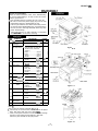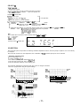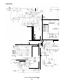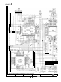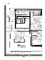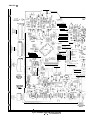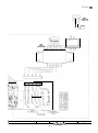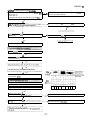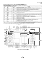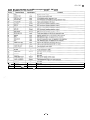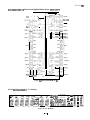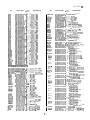
1
CD-C471W
SHARP SERVICE MANUAL
No. S6845CDC471 W/
CD-C471 W
CD-C471 W mini component system consisting of
CD-C471 W mini component system, front (CP-C471), senter
(GBOXS0006AWM6)and surround(GBOXS0007AWM6)
Speaker System.
l
In the interests of user-safety the set should be restored to its
original condition and only parts identical to those specified be
used.
ciInli%
DIGITAL AUDIO
YYI
SURROUND
P R O f L O G I C
Manufactured under license from Dolby Laboratories Licensing Corporation.
DOLBY, the double-D symbol 00 and “PRO LOGIC”
are trademarks of Dolby Laboratories Licensing Corporation.
/
.
CONTENTS
Page
SAFETY PRECAUTION FOR SERVICE MANUAL ..........................................................................................................
VOLTAGE SELECTION.. ..................................................................................................................................................
SPECIFICATIONS ............................................................................................................................................................
NAMES OF PARTS ..........................................................................................................................................................
OPERATION MANUAL .....................................................................................................................................................
DISASSEMBLY.. ...............................................................................................................................................................
REMOVING AND REINSTALLING THE MAIN PARTS.. ................................................................................................
ADJUSTMENT.. ..............................................................................................................................................................
NOTES ON SCHEMATIC DIAGRAM .............................................................................................................................
TYPE QF TRANSISTOR AND LED ................................................................................................................................
BLOCK DIAGRAM ..........................................................................................................................................................
SCHEMATIC DIAGRAM /WIRING SIDE OF P.W.BOARD.. ..........................................................................................
WAVEFORMS OF CD CIRCUIT.. ...................................................................................................................................
TROUBLESHOOTING (CD CHANGER CONTROL / CD SECTION). ............................................................................
FUNCTION TABLE OF IC ..............................................................................................................................................
FL DISPLAY ....................................................................................................................................................................
REPLACEMENT PARTS LIST/EXPLODED VIEW
SHARP CoRPoRATloN
2
2
3
4
6
7
IO
11
14
14
15
18
39
40
44
54
This document has been published to be used
for after sales selvice only.
The contents are subject to change without notice.
CD-C471 W
SAFETY PRECAUTION FOR
SERVICE MANUAL
Laser Dkode Properties
Material: GaAlAs
Wavelength. 780 nm
Emission Duration: continuous
Laser Output: max. 0.6 mW
Precaution to be taken when replacing and servicing the
Laser Pickup.
The AEL (Accessible Emission Level) of Laser Power Output
forthis model is specified to belowerthan Class I Requirements.
However, the following precautions must be observed during
servicing to protect your eyes against exposure to the Laser
beam
(1) When the cabinet has been removed, the power is turned
on without a compact disc, and the Pickup is on a position
outerthan the lead-in position, the Laserwill Iightforseveral
,seconds to detect a disc, Do not look into the Pickup Lens.
(2) The Laser Power Output of the Pickup inside the unit and
replacement service parts have already been adjusted prior
to shipping.
(3) No adjustment to the Laser Power should be attempted
when replacing or servicing the Pickup.
(4) Under no circumstances look directly into the Pickup Lens
at any time.
(5) CAUTION - Use of controls or adjustments, or performance
of procedures other than those specified herein may result
in hazardous radiation exposure.
CAUTION
0 This Mini Component System is classified as a CLASS
1 LASER product.
0 The CLASS 1 LASER PRODUCT label is located on the
rear cover.
l Use of controls, adjustments or performance of procedures other than those specified herein may result in hazardous radiation exposure.
As the laser beam used in this compact disc player is
harmful to the eyes, do not attempt to disassemble the
cabinet. Refer servicing to qualified personnel only.
1
VOLTAGE SELECTION
The voltage selector is located on the AC voltage selector box. If adjustment is necessary, use a screwdriver in order to turn the
selector in either direction the correct voltage figure is displayed in the window next to the adjustment screw.
QACCB0002AWOO
92LCORD5776
QACCE0005AWOO
QACCL0002AWOO
92LPLUG027
92LCORDZ1652A
El
Figure 2 POWER SUPPLY CORD AND PLUG ADAPTOR
-2-
92LPLUG155A
CD-C471 W
FOR A COMPLETE DESCRIPTION OF THE OPERATION OF THIS UNIT, PLEASE REFER
TO THE OPERATION MANUAL.
SPECIFICATIONS
l
0 General
Power source:
Power consumption:
Dimensions:
Weight:
AC 11 O/l 27/2201230-240 V,
50160 Hz
112w
Width; 270 mm (1 O-5/8”)
Height; 303 mm (1 l-l 3116”)
Depth; 350 mm (13-13/16”)
7.1 kg (15.3 Ibs.)
Bias and erasure
system:
Tape speed:
Wow and flutter:
Heads:
0 Amplifier section
Output power:
Input terminals:
Output terminals:
PMPO; 1,000 W (total)
Front speakers;
MPO; 176 W (88 W + 88 W)
(10 % T.H.D.)
RMS; 80 W (40 W + 40 W)
(10 % T.H.D.)
Center speaker;
MPO; 32 W (10 % T.H.D.)
RMS; 20 W (10 % T.H.D.)
Surround speakers;
MPO; 32 W (10 % T.H.D.)
RMS; 20 W (10 % T.H.D.)
Video/Auxiliary (audio signal) x 2;
500 mVl47 kohms
Front speakers; 6 ohms
Center speakers; 4 ohms
Surround Speakers; 8 ohms
Headphones; 16-50 ohms
(recommended; 32 ohms)
DIR Converter:
Frequency response:
Dynamic range:
l
Compact cassette tape
50 - 14,000 Hz (Normal tape)
DC motor with electronic governor x 1
55 dB (TAPE 1, playback)
50 dB (TAPE 2, recording/playback)
AC
4.76 cmlsec. (l-718 ips)
0.15 % (WRMS)
TAPE-l : Playback x 1
TAPE-2: Record/playback x 1
Erase x 1
0 Front speaker section
3-way type [130 mm (5-l/8”) woofer,
50 mm (2”) tweeter and super tweeter]
Maximum input power: 80 W
Impedance:
6 ohms
Dimensions:
Width; 200 mm (7-7/8”)
Height; 300 mm (11-13/l 6”)
Depth; 253 mm (10”)
Weight:
2.7 kg (5.8 Ibs.)/each
T y p e :
l
Center speaker section
Type:
100 mm (4”) full-range speaker
Maximum input power: 40 W
Impedance:
4 ohms
Dimensions:
Width; 262 mm (1 O-5/1 6”)
0 Compact disc player section
Type:
Signal readout:
Cassette deck section
Type:
Frequency response:
Motor:
Signal/noise ratio:
3-disc multi-play compact disc player
Non-contact, 3-beam semi-conductor
laser pickup
1 -bit D/A converter
20 - 20,000 Hz
90 dB (1 kHz)
Weight:
Height; 145 mm (5-3/4”)
Depth; 201 mm (7-15/l 6”)
1.2 kg (2.6 Ibs.)/each
Tuner section
Frequency range:
l
FM; 88 - 108 MHz
AM; 531 - 1,602 kHz
Surround speaker section
Type:
100 mm (4”) full-range speaker
Maximum input power: 20 W
Impedance:
8 ohms
Dimensions:
Width; 170 mm (6-3/4”)
Weight:
Height; 122 mm (4-l 3/l 6”)
Depth; 176 mm (6-1916”)
0.7 kg (1.5 Ibs.)/each
Specifications for this model are subject to change without
prior notice.
-3-
CD-C471 W
NAMES OF PARTS
n Front Panel
1. (CD) Disc Tray
2. (CD) Disc Number Select Buttons
3. (CD) Disc Skip Button
4. (CD) Open/Close Button: 4
5. (CD) Play Indicator: )
6. (CD) Repeat Indicator: 4
7. (CD) Pause Indicator: 11
8. (CD) Disc Number Indicators
9. Dolby Pro Logic Indicator
10. Sleep Indicator
11. (TUNER) FM Stereo Mode Indicator: ST
12. (TUNER) FM Stereo Indicator: a,
i3. Extra Bass Indicator: X-BASS
14. (CD/TUNER) Memory Indicator
15. (TAPE) Direction Indicators
16. (TAPES) Reverse Mode indicator: c-I
17. (TAPEP) Record indicator
18. Timer Indicator
19. Spectrum AnalyzerNolume Level/Balance Indicator
f567
8
10
9
20. On/Stand-by Button
21. Bypass Button
22. Center Mode Buttons: NORMAL/PHANTOM
23. Extra Bass Button: X-BASS
24. Volume Up/Down Buttons: ~1~7
25. Function Selector Buttons
26. Headphone Socket
I
15 16 17 18 19
2324
27. Clock Button
28. Timer/Sleep Button
29. (TAPES) Record Pause Button: l 11
30. (CD/TAPE) Stop Button: n
31. Equalizer Selector/Demo Mode Button
32. CD Edit Button
33. Tape 1 Edit Button
34. Tuning and Time Up/Down Buttons: ,,/,..,
35. Memory/Set Button
36. (CD) Track Down/Review Button: u/w
(TUNER) Preset Down Button: a/~(
(TAPEP) Fast Wind Button: ++
37. (TAPE 2) Reverse Play Button: 4
38. (TAPE 1) Play Button: )
(TAPE 2) Forward Play Button: )
(CD) Play/Repeat Button: ) 4
39. (CD) Track Up/Cue Button: ))/))1
(TUNER) Preset Up Button: ))/))1
(TAPE2) Fast Wind Button: ))
40. (TAPES) Reverse Mode Button
25
26
27 28 29
30
1
3132 33
3435 36 37 38 39 40
41
41. (TAPE 1) Cassette Compartment
42. (TAPE 2) Cassette Compartment
-4-
42
j
CD-C471 W
n Rear Panel
-4
1. CD Digital Output Socket
2. AC Voltage Selector
3. AC Power Input Socket
4. AM Aerial Terminal
5. Aerial Earth Terminal
6. FM 75 Ohms Aerial Terminal
7. Video/Auxiliary (Audio Signal) Input Sockets
8. Sub Woofer Output Socket
9. Span Selector Switch
10. Front Speaker Terminals
11. Center Speaker Terminals
12. Surround Speaker Terminals
I6
/l/l/1!/ I I llllll
llilllllflillillflil
llilllilllllllliliil ~ llilllll I I lliill
Left speaker
n Speaker Section
0 Front Speaker
1. Super Tweeter
2. Tweeter
3. Woofer
4. Bass Reflax Duct
5. Speaker Wire
0 Center Speaker
6. Full-Range Speaker
7. Speaker Wire
0 Surround Speaker
6
8. Full-Range Speaker
9. Speaker Wire
n Remote Control
1. Remote Control Transmitter LED
2. Surround Level Buttons: ,,I,,
3. Center Level Buttons: V/A
4. Dolby Pro Logic Button
5. Center Mode Button
6. Test Tone Button
7. Balance Control Buttons: < / >
0 Tuner control section
8. Preset Up/Down Button: ,,jA
l CD Control section
9. Disc Skip Button
10. Play/Repeat Button: )4
11. Memory Button
12. Clear Button
13. Pause Button: 11
14. Track Down/Review Button: q/f++
15. Track Up/Cue Button: ))/)H
16. Stop Button: q
17. Random Button
l Tape control section
18. (TAPE 2) Reverse Play Button: +
19. (TAPE l/2) Stop Button: n
20. (TAPE 1) Play Button/
(TAPE 2)
21. (TAPE 2)
22. (TAPE 2)
23. (TAPE 2)
Forward Play Button: )
Record Pause Button: 011
Fast Wind Button: ++
Fast Wind Button: ))
0 Common section
24. Equalizer Mode Button
25. Function Selector Buttons
26. On/Stand-by Button
27. Extra Bass Button: X-BASS
28. Volume Up/Down Buttons: o/a
3
4
9
10
6
7
II
18 192021
/
I I I
24
25
26
27
-5-
8
5
22
23
28
In thts example, the clock is set for the
24-hour (0:OO) system.
1 Press the ON/STAND-BY button to enter the stand-by mode.
2 Press the CLOCK button.
3 Within
" 5 seconds, press the MEMORY/SET button.
4 Press the TUNINGmIME (vor~) button to select the time
display mode.
“0:00”
TUNING/’
TIME
(,/fi)
I
MEMORY/
SET
+ The 24.hour display will appear.
(0:OO 23:59)
“AM 1200’ + The la-hour display will appear.
(AM or PM 12:OO 11:59)
“AM 0:OO” + The 12-hour display will appear.
(AM or PM 0:OO - 11:59)
Notes concerning use:
l
Replace the batteries if the operating distance becomes reduced or if operation becomes erratic.
l
--1----
0.2 m 6 m
(6” 20’)
Periodically clean the transmitter LED on the remote control
and the sensor on the main unit with a soft cloth.
l
Exposing the sensor on the main unit to strong light may
interfere with operation. Change the lighting or the direction
of the unit.
l
Keep the remote control away from moisture, excessive heat,
shock, and vibrations.
I
0 Note that this can only be set when the unit is first installed
or it has been reset (see page 30).
5 Press the MEMORY/SET button.
6 Press the TUNINGmIME ( v or A) button
to adjust the hour.
0 Press the TUNlNGfllME (v or A) button once to advance
the time by 1 hour. Press for more than 0.5 seconds to advance continuously.
\\if/
1-II, n,-I Cl1-t
,i,!\
4
0:OO -AM 12:OO - AM 0:OO
+
+
51
0 When the 12.hour display is selected, “AM” will change automatically to “PM”.
7
8
l
Press the MEMORY/SET button.
Reset the microcomputer under the following conditions:
Press the TUNING/TIME( v or F. ) button to adjust the
minutes.
l
Press the button for at least 0.5 seconds to change the time
in 5-minute intervals.
l
l
0 The hour setting will not advance even if minutes advance
from “59” to “00”.
9 Press the MEMORY/SET button
l
The clock starts operating from “0’seconds. (Seconds are not
displayed.)
Note:
l
In the event of a power failure or when the AC power lead
is disconnected, the clock display will go out.
When the AC power supply is restored, the clock display will
flash on and off to indicate the time when the power failure
occurred or when the AC power lead was disconnected.
If this happens, follow the procedure below to change the
clock time.
To change the clock time:
To see the time display:
When the unit is in the stand-by mode
l When the unit is in the demonstration mode, press
the DEMO button to enter the clock mode.
Press the CLOCK button.
l The time display will appear for about 5 seconds
a Press the MEMORY/SET button
To change the time display mode:
Q Perform steps 6 - 9 above.
Q Press the ON/STAND-BY button to enter the stand-by mode.
0 Whilst pressing down the VOLUME v button and the TUNINGiTlME A button, hold down the ON/STAND-BY button for
at least 1 second.
Q Periorm steps 6 - 9 above.
When the unit is on:
(?? Press the CLOCK button.
Q Within 5 seconds, press the MEMORY/SET button
0 Perlorm steps 6 - 9 above.
Caution:
l
The operatiow’explained above will erase all data stored in
memory including clock and timer settings, and tuner and CD
presets.
To erase all of the stored memory contents (clock and timer
settings, and tuner and CD presets).
If the display is not correct.
If the operation is not correct.
Note:
l
To erase the tuner preset memory see “To erase all of the
contents of preset memory” on page 16.
1 Press the ON/STAND-BY button to enter the stand-by mode
2 While pressing down the VOLUME v button and the TUNINGRIME A button. hold down the ON/STAND-BY button for
at least 1 second.
CD-C471 W
DISASSEMBLY
Caution on Disassembly
Follow the below-mentioned notes when disassembling
the unit and reassembling it, to keep it safe and ensure
excellent performance:
1, Take cassette tape and compact disc out of the unit.
2. Be sure to remove the power supply plug from the wall
outlet before starting to disassemble the unit.
3. Take off nylon bands or wire holders where they need to
be removed when disassembling the unit. Afterservicing
the unit, be sure to rearrange the leads where they were
before disassembling.
4. Take suffcient care on static electricity of integrated
circuits and other circuits when servicing.
REMOVAL
iTEF
TOD Cabinet
1
Side Panel
2
(Left/right)
CD Player Unit/
3
CD Tray Cover
4
Back Board
5
Tuner PWB
6
Main PWB
7
Front Panel
8
9
10
14
15
PROCEDURE
FIGURE
1. Screw ..................... (Al) x4
1. Screw ..................... (Bl) x6
7-1
7-l
1. Turn on the power supply,
open the disc tray, take out
the CD cover, and close.
(Note 1)
2. Hook ...................... (Cl) x3
3. Hook ...................... (C2) x2
4. Screw .................... (C3) xl
5. Socket ................... (C4) x3
1. Screw .................... (Di) x13
2. Socket ................... (D2) x l
1. Screw .................... (El) xl
2. Socet ..................... (E2) xl
1. Screw .................... (Fl) xl
2. Socket ................... (F2) x2
3. Flat Wire.. .............. (F3) x2
4. Tip Wire.. ............... (F4) xl
5. Socket ................... (F5) xl
1. Screw .................... (Gl) x2
2. Hook.. .................... (G2) x2
1. Screw .................... (Hl) x12
7-2
Display PWBI
Switch PWB
Tape Mechanisn 1. Open the cassette holder.
2. Screw .................... (Jl) x5
Power Amo. PWE 1. Screw .................... (Kl) x4
2. Socket ................... (K2) x2
3. Push Rivet ............ (K3) x4
CD Servo PWB
1. Screw .................... (Ll) xl
2. Cover .................... (L2) x4
Turntable
1. Screw .................... (Ml) xl
2. Cover .................... (M2) x l
CD Player Base 1. Screw .................... (Nl) x2
2. Guide .................... (N2) x2
CD Changer
1. Screw .................... (Pl) x4
Mechanism
CD Mechanism 1. Screw .................... (Cl) xl
Figure 7-l
m CD Tray Cover
8-1
8-l
a-2
8-2
a-3
a-3
8-4
Figure 7-2
8-5
8-6
8-6
8-7
8-7
LOCK
Note 1:
How to open the changer manually. (Fig.7-3)
1. Insert the tip of fine screwdriver into the hole of CD player
base, and press down the worm wheel c A >
2. Then, turn fully the lock lever in the arrow direction through
the hole on the loading chassis bottom in this state.
After that, push forward the CD player base.
Figure 7-3
-7-
Hook
lT?F-?l
Front Panel
Tuner
PWB
( Li ) xl
03 xlOmm
CD Servo P W B
m* Main PWB
03
x8mm
Loading Chassis
03 xl Omm
Figure 8-5
Figure 8-1
(M2)xl
Washer
I
Turntable
-w /
03 xl Omm
(% ) x203 x’Omm
03 x8mm
Figure 8-2
Switch PWB
Figure 8-6
03
xl Omm
(Qi)xl
02.6 xl Omm
lolder
(Left/Right)
Figure 8-3
Power
(Kl)x4
03 xl 2mm
Be careful when installing the CD changer mechanism.
Install the CD changer mechanism on the CD player base after
the shift lever has been set in the highest position.
PWB
Figure 8-7
Figure 8-4
-8-
CD-C471 W
r/RE;pz!Ae;
IF]
PROCEDURE
1
1
2.
3.
4.
5.
Net ..........................
Fromt Panel ...........
Screw .....................
Screw .....................
Screw .....................
(Al) xl
(A2) xl
(A3) x2
(A4) x4
(A5) x2
Tweeter A
Front Panel
W);l
Note:
The center and SURROUND speakers can be easily disassembled. Therefore the disassembling method is not discribed.
For details refer to the disassembling drawing in the Parts
Guide.
cl
Woofer
Screwdriver
Figure 9-1
Super
Tweeter
(A4)x4
64 xi 4mm
--AXI I
\
Woofer
Figure 9-2
-9-
/
CD-C471 W
REMOVING AND REINSTALLING THE MAIN PARTS
CD MECHANISM SECTION
Perform steps 1, 2, 3, 14 and 15 of the disassembly method
to remove the CD mechanism.
Turntable Up/Down M
How to remove the turntable up/down motor
(See Fig. IO-I)
1, Remove the screws (Al) x 2 PCS., to remove the turntable
up/down motor.
02 x5mm
Figure 10-l
How to remove the pickup (See Fig. 10-2)
1. Remove the screws (Bl) x 2 PCS., to remove the shaft (B2)
x l pc.
2. Remove the stop washer (B3) x 1 PC., to remove the gear
(B4)x 1 pc.
3. Remove the pickup.
( B2 ) xl
Gear
( B4 ) xl
Figure 10-2
-lO-
CD-C471 W
ADJUSTMENT
TUNER SECTION
MECHANISM SECTION
l
Torque Meter
Specified Value
Tape 1: Over 80 g
Tape 2: Over 80 g
Play: TW-2412
l
Torque Check
Torque Meter
Specified Value
Tape 1
Play: TW-2111
Fast forward: TW-2231
Rewind: TW-2231
l
fL: Low-range frequency
fH: High-renge frequency
l AM IF/RF
Signal generator: 400 Hz, 30%, AM modulated
Driving Force Check
Tape 2
30 to 60 g. cm
-
30 to 100 g.cm
50 to 100 g.cm
50 to 100 g.cm
Normal
speed
Ml-T-1 11
Setting/ Instrument
Adjusting Connection
Parts
IF
450 kHz
AM Band Coverage
AM
990 kHz
Tracking
T351
*1
(fL): T 3 0 6 “2
1.1 * 0.1 v
(fL): T 3 0 2 *1
*l. Input: Antenna,
*2. Input: Antenna,
Tape Speed
Test Tape
Test Stage Frequency Frequency
Display
Adjusting
Point
VRMl
1,602 kHz
531 kHz
990kHz
Output: TP302
Output: TP301
Specified Instrument
Value
Connection
3,000 f
30 Hz
Notes:
1: Description of the “FM IF Adjustment” is not carried on this
Manual. It is because the IF coil in the FM front end section
has been best adjusted in the factory so that its further
adjustment is not needed at the field. When replacing the
FM front end assembly, no adjustment is needed either.
2: The parts in the FM front end section are prepared in a
complete unit, so you can’t obtain each part individually
Speaker
terminal
\
* FM Mute Level
Signal generator: 1 kHz, 40 kHz dev., FM modulated
TAPE MECHANISM PWB
i
/ TUNER PWB /
I
T306
T351
l- - -D
I
AM
TRACKING
AM BAND
COVERAGE
Figure 11 ADJUSTMENT POINTS
-ll-
50301
ANTENNA
TERMINAL
CD-C471 W
TEST MODE
l
Setting the test mode
Any one of test mode can be set by pressing several keys as follows.
<REC. PAUSE> + <CD> + <POWER>
TEST: CD operation test
l TEST mode
Function - CD test mode
Sytting of TEST mode
1
In;fication of CD TST mode (Fig.l2-1)
OPEN/CLOSE operation is manual operation.
IL is not performed.
Thk pickup can be moved by using the ())) or (M) key.
<MEMORY>
<MEMORY>
<STOP>
<MEMORY>
LASER ON - Tracking on the spot. - Tracking on the spot. - STOP
SERVO OFF PLAY
SERVO ON PLAY
t <PLAY> key input- TOC. IL is performed, and the ordinary PLAY is performed. - Press <STOP> key. - Stop
if the following key is pressed during PLAY, it is possible
to specify directly any Track No.
<Disc Number 1, key: Track 4
<Disc Number 2> key: Track 9
<Disc Number 3> key: Track 15
Note:
Only in STOP state it is possible to slide the pickup with the ())) or (q) key.
VOL. --- Last memory
BAL. --- CENTER
R.GEQ. --- FLAT
X-BAS --- OFF
Canceling method - POWER OFF
I
Figure 12-1
CD SECTION
Since this CD system incorporates the following automatic adjustment function, when the pickup is replaced, it is not necessary
to readjust it.
Since this CD unit does not need adjustment, the combination of PWB and laser pickup unit is not restricted.
Automatic adjustment item
1. Focus offset (Fig.1 2-2)
2. Tracking offset (Fig.12-3)
3. E/F balance (tracking error balance) (Fig.12-4)
4. RF level AGC function (HF level: constant)
5. RF level automatic follow-up of the tracking gain
l
This automatic adjustment is performed each time a disc is changed. Therefore,
each disc is played back using the optimal settings.
0.1s
0.50 v
ICl @ FE
Enlarged
VIFM
10ms
0.50 v
ICI @ FE
FOCUS
OFF-SET
ADJUST
1 Oms
0.50 v
ICI @TE
0.1s
0.50 v
ICI @ TE
t
Figure 12-3
Figure 12-2
TRACKING/
ERROR
BARANCE
ADJUST
200
1 V/d
IC 1
Figure 12-4
-12-
1
i
TRACKING
OFF-SET
ADJUST
I
j
TRACKING
OFF-SET
, ADJUST
CD-C471 W
EXPLANATION OF DOLBY SURROUND PRO LOGIC AND EVALUATION METHOD
Outline
In the normal mode of Pro Logic ON mode the amplifiers for
C-ch and S-ch are in operative state, so that the SP output
appears.
l In the Phantom mode of Pro Logic ON mode the amplifier for
C-ch is in MUTE state, so that the SP output is cut. The
amplifier for S-ch (surround) is in operative state, so that the
SP output appears
l
Namely, two speakers are connected in parallel to one
amplifier.
In the Pro Logic BYPASS mode the amplifierfor C-ch (center
channel) and the amplifier for S-ch (surround channel) are in
MUTE state. The SP output is cut.
l
State of element output and terminal output in specific mode
l
Dolby Pro Logic On mode
Dolby Pro Logic
1 Output enabled state
Output enabled state
IC501 1 12 pin L-out Output enabled state
Output enabled state
Output enabled state
1 Output enabled state
1 No output
/ Output enabled state
11 pin R-out Output enabled state
IC501’ / 9 pin C-out 1 No output
Phantom mode
Normal mode
Bypass mode
L
l
1 Output enabled state
/ 10 pin S-out / No OutDut
I Output enabled state
I L-ch I Output enabled state
SP OUT
Output enabled state
R-ch ,Output enabled state
(SO901)
No output in MUTE (Q604) state Output enabled state
SP OUT C-ch
IC501
(SO901 )
SP OUT S-ch
No output in MUTE (Q603) state
I
/ Output enabled state
Output enabled state
No output in MUTE (Q604) state
Output enabled state
Output enabled state
(SO901 )
Test tone output
l Pro Logic ON Normal mode
Press the remote control TEST TONE button.
--+Output of only L-ch +Output of only C-ch
1
-r
Output of only S-ch t Output of only R-ch
The test tone (noise) is repeatedly output for output period
(2 set).
In this case the following indication appears repeatedly.
-TEST +L-ch -Gch
T
L
S-ch t R-ch
l Pro Logic ON Phantom mode
Press the remote control TEST TONE button.
+Output of only L-ch -tOutput of only R-ch
I1
t Output of only S-ch
The test tone (noise) is repeatedly output for output period
(2 set).
Almost no output (only omitting component)
(SO901) SP out C-ch
Almost no output (only omitting component)
(SO901) SP out S-ch
Input signal is output.
Output point
SP out
(SO901)
l
l
(50901) SP out S-ch
Almost no output (only omitting component)
Almost no output (only omitting component)
Almost no output (only omitting component)
Relation between VIDEO IN input and output in Pro Logic
ON state
(1) L-ch/R-ch same phase input into VIDEO IN input jack in
VIDEO Function mode
(SO901) SP out C-ch
SP cut, no output
(SO901) SP out S-ch
(2) L-ch/R-ch reverse phase input into VIDEO IN input jack in
VIDEO Function mode
(Reverse phase: Phase difference between L and R is 180”)
In this case the following indication appears repeatedly.
-+TEST + L-ch + R-ch
1‘
.L
t S-cht
Almost no output (only omitting component)
Almost no output (only omitting component)
Input signal is output.
(SO901) SP out C-ch
-13-
Phantom mode
L-ch 1Almost no output (only omitting component)
R-ch Almost no output (only omitting component)
(SO901) SP out C-ch
SP cut, no output
(SO901) SP out S-ch
Input signal is output.
Accordingly, if you want to output signal waveform to C-ch SP
out, give the same phase input into L-ch/R-ch INPUT in the
Pro Logic Normal mode.
If one of channels receives input, C-ch does not output. Only
L-ch or R-ch outputs.
If you want to output signal waveform to S-ch SP out, you can
use either Normal mode or Phantom mode. However, 180”
reverse phase input must be given to L-ch/R-ch INPUT.
CD-C471 W
NOTES ON SCHEMATIC DIAGRAM
l
l
l
Resistor:
To differentiate the units of resistors, such symbol as K and
M are used: the symbol K means 1000 ohm and the symbol
M means 1000 kohm and the resistor without any symbol is
ohm-type resistor. Besides, the one with “Fusible” is a fuse
type.
Capacitor:
To indicate the unit of capacitor, a symbol P is used: this
symbol P means micro-micro-farad and the unit of the
capacitor without such a symbol is microfarad. As to
electrolytic capacitor, the expression “capacitance/withstand
voltage” is used.
(CH), (TH), (RH), (UJ): Temperature compensation
(ML): Mylar type
(P.P.): Polypropylene type
Schematic diagram and Wiring Side of P.W.Board for this
model are subject to change for improvement without prior
notice.
REF. NO
DESCRIPTION
l
l
The indicated voltage in each section is the one measured
by Digital Multimeter between such a section and the chassis with no signal given.
1. In the tuner section,
( ) indicates AM
2. In the main section, a tape is being played back.
3. in the deck section, a tape is being played back.
( ) indicates the record state.
4. In the power section, a tape is being played back.
5. In the CD section, the CD is stopped.
Parts marked with “A ” ( c - - 7) are important for
-mm
maintaining the safety of the set. Be sure to replace these
parts with specified ones for maintaining the safety and
performance of the set.
POSITION
SW1
OPEN/CLOSE
ON-W
SW71 1
SW712
SW718
SW719
SW721
SW723
TAPE
ON-E
/ SW801
VIDEO/AUX
CENTER MODE/PHANTOM
CENTER MODE/NORMAL
ON-E
ON-m
SWM 3
ON-E
ON-CJj--J
ON--m
DOLBY PRO LOGIC BYPASS
REC PAUSE
ECB
u)(2)(3)
KTAI 268
KTA1271
KTC3199
KTC3203
GR
Y
GR
Y
/ VOLTAGE SELECTOR
1 110-127220-230-240
SWM 5
REC FWD
REC RVS
F.A.S.
ON--~
ON--E
ON-W
SWM 6
CAM
ON--QE4
SWM4
+H-
(3)(2x1)
KVl236223F
Figure 18 TYPES OF TRANSISTOR AND LED
-14-
333GTH2
PICKUP UNIT
CNP99
DIGITAL
OUT
ry
‘t
i.
CNPI 1
t
FM0 SERVO/SIGNAL
FMIN
FOCUS COIL
*-t
TRACKING COIL
-.t
RES. CQCK. COIN
SQOUT. RWC. WRQ
t
DAT. SELIAL CONTROUCE
.I
SKI
MOTOR
D?&
MOTOR
SLt. SL-. DRF
OPEN/CLOSE
b+Bl
n,
PICKUP IN
SW4
t
/
CNPIP
-
I I
c
Ill
i
r------- ----__-__
I
Figure 16 BLOCK DIAGRAM (2/3)
-16-
I
CD-C471 W
w
‘UTER
lC56115621563
N5M4558L
lC562(1/2)
Figure 17 BLOCK DIAGRAM (3/3)
- 17-
CD-C471 W
L
-
TRT&t
FOC
Fc-.
GND
I
85
201
PDVR
i
-
I
-
-
PICKUP UNIT
- - - - - -
-
-
0”
------_
0”
0”
-
2”
2”
25”
2%
-
25”
4.7”
07”
I
1
WOTOR
- PWB3
-
L-.-.-.--.-... -.-.--.-.-CNKq$&
l
The numbers 0 to @ are waveform numbers shown in page 39.
l
NOTES ON SCHEMATIC DIAGRAM can be found on page 14.
1
I
2
I
3
I
4
Figure 18 SCHEMATIC DIAGRAM (l/13)
-18-
I
5
I
b
I
CD-C471 W
H CD SIGNAL
CD
DIGITAL
OUT
1.-.-.L
JACK PWB-A4
H CD SIGNAL
SERVO PWB-C.Lj
.-.-.-.__.~ i_cD
._-,~
7
a
9
10
Figure 19 SCHEMATIC DIAGRAM (Z/l 3)
-19-
11
12
I
CD-C471 W
l
NOTES ON SCHEMATIC DIAGRAM can be found on page 14.
1
2
4
3
Figure 20 SCHEMATIC DIAGRAM (3/13)
- 20 -
5
6
CD-C471 W
MAIN PWB-A1(1/2)
L.-.-.-.
-
w FM SIGNAL
_,..
- PLAYBACK SIGNAL
,s~E
= RECORD SIGNAL
H CD SIGNAL
cmc
155133
R463
HEADPHONE AMP.
10
9
Figure 21 SCHEMATIC DIAGRAM (4/13)
-2l-
11
12
I
CD-C471 W
------_
WE MECHANISM PWB-F 7
I
I
SWM4
RECRVS
v
c
_
A
1
LLL--J
1
1
L-CH
TAPE1
PLAYBACK HEAD
I
I
/
‘106
II
I
1
RI36 Ic136
i.8K )470?
/
2SC1845 F
-
Q10.5
2SC1845F
RECIP.6.
RI91
ill
I
:
I’
I
’
h
l- ---------- ------------i
l
NOTES ON SCHEMATIC DIAGRAM can be found on page 14.
1
2
4
3
Figure 22 SCHEMATIC DIAGRAM (5/l 3)
-22-
5
6
CD-C471 W
-----
,_-------------r--------
FIN PWB-A1(2/
I
TT
E
1i
i;
5
+B
,, 18
KRC104 M
SWITCHING
158
$+B
%cF
Q124
KTA1266 GR
SWITCHING
R166 RI67
= PLAYBACK SIGNAL
= RECORD SIGNAL
-
7
8
9
10
Figure 23 SCHEMATIC DIAGRAM (6/13)
- 23 -
11
12
1
CD-C471 W
A
I
I
FL701
E
l
I
I
I
I
I
I
I
C
.-. -.
lXOl70AW
SYSTEM MICROCOMPUTER ;
D
l III L-L---
E
I I I
‘
I1IIIlI
I
///II/
I
‘
II/I I
F
I) FM SIGNAL
I
G
JK700
HEADPHONES
H
l
NOTES ON SCHEMATIC DIAGRAM can be found on page 14.
1
2
4
3
Figure 24 SCHEMATIC DIAGRAM (7/l 3)
- 24 -
5
6
CD-C471 W
_--------_
--------_--------6: ,
DlSCl
DISC2
u,‘LED716
:I LED716
51
41
LED715
DISC3
::I
31
21
3r
LED714
FW701
I,%Y ,
LED714-LED719’333GTHZ
1----P--------_-m-_
DISPLAY PWB-A3 1
FW701-2
R749
IOK
I/
LED719.d
LED717 :I
I-------__----_
1
I,
IT2 :
R779.., IOK
R780,,, 1 AK
R761..I 10K
4,
//I
/
I
EM
GZ
18 17 16 15 14 13 1 1, 10
paggaassa
hhhhhhhhh- IC702
<z
lt9g,-,,,
>OOJOOOOD
!I”
I
/
BU2092F
INPUT/OUTPUT EXPANDER
R741... IK
>u LED705 ,333GTH2 REV
R740.., IK
<; LED704
333GTH2 REW
R739... 1K
‘
tu LED703
333GTHP STOP
R736,.. ,K
\:: LED702
333GTH2 FF
R737... 1K
-. : LED701
T333GTH2 PLAY
4
I
FLAT CABLE(263)
7
8
9
10
Figure 25 SCHEMATIC DIAGRAM (8/13)
- 25 -
11
12
I
CD-C471 W
.-.-.-.P.-.-.-.-.P.-.-.-.r
IC901
STK40704
POWER AMP.
A
I
:901
6
R905
-f
I
I
I
&
8:
I
I
1
I
w:o1\
L:OF
c!9(
I
KT*IIDRR GR
C
r
REAR
A_GND
-
CHASSIS
GND
CENTE
I
D
-
c910
b 2200150
I
+B
-
E
F
G
I
“F2
i
~WER
PWB-B 1
.-.-.w-.-.-.-.P.-.p.p-
H
l
~
CHASSIS
GND
NOTES ON SCHEMATIC DIAGRAM can be found on page 14.
1
2
3
4
Figure 26 SCHEMATIC DIAGRAM (9/I 3)
- 26 -
5
6
CD-C471 W
m-.-.-.-*-.-.-.-.-.-_-.-
I) FM SIGNAL
R969
68
.K
M901
FAN MOTOR
Ji
,”
: h^
I
)901
‘EAKER
iRMlNAL
0903
IC951
LA4450
POWER AMP.
HCJN
LOFF
r-
]
L-W
]
R-CH
1
I- 1
R CH
C938
47135
*
MIN.
CENTER
4 OHMS
MIN.
] I-CH
, f
;;;;s
A c941
0.022
T
.
",TI
=E(ML)
C960
FRONT
6 OHMS
MIN.
I
z
w
6
1
2
3
4
5
a
9
10
Figure 27 SCHEMATIC DIAGRAM (10113)
- 27 -
11
12
1
CD-C471 W
VD301-1
KV1236Z23F
piicm-j
ANTENNA
R319
I
VD301-2
KVI 236223F
AM
R324
SE-
GND
C336
: X47OP
FM
750hms
CHASSIS
GND
CHASSIS
GND
FE301
FM FRONTEND
I
I
I
I
I
I) FM SIGNAL
+B
0 AM SIGNAL
I
I
I
I
m-----wI- --------------
* NOTES ON SCHEMATIC DIAGRAM can be found on page 14.
1
I
2
3
I
4
Figure 28 SCHEMATIC DIAGRAM (1 l/13)
- 28 -
I
5
I
D
I
CD-C471 W
p-----P---p-pP- -- r- -----
TUNER PWB-t-h
I
I
I
I
I
I
I
I
I
I
I
I
I
I
R354
. ..3.9K
I
ZD351
MTZJ5.1 f
I
I
I
I
I
I
nI
I
I
a
3ov
(3~3'4
t
I
1
R387
22K
Cl361
KRC107 M
”MPX PHASE
KTAI 266 GR
I
D351 n
lSS133
--
L
ZD352
MTZJ3.9B
I
I
I
I
---m-s-- -_-_-B
7
a
9
10
Figure 29 SCHEMATIC DIAGRAM (12/13)
- 29 -
11
12
I
CD-C471 W
( ):CD NORMAL REC
OTHERCD NORMAL PLAY
I
2
I
3
I
4
Figure 30 SCHEMATIC DIAGRAM (13/l 3)
- 30 -
5
6
CD-C471 W
DISPLAY PWB-A2
1’ SWICH PWB-A3 1
1
7
8
9
10
Figure 31 WIRING SIDE OF P.W.BOARD (l/E)
-31 -
11
12
I
CD-C471 W
FLAT CABLE(263
1
24
c
CNS12
FWMI ’
1
E
MECHANISM
P34 1-E
F
TO HEAD PWB
P34 2-F
I
G
CNSI 1
H
TO TUNER PWB
P38 2-c
1
2
/
3
4
Figure 32 WIRING SIDE OF P.W.BOARD (2/8)
- 32 -
5
6
CD-C471 W
TO POWER PWB
P36 2-D
/I
50/9
:i
FM/AM(KHz)
1 100/i 0
SW201
SPAN SELECTOR
.JK451
SUB
WOOFER
-Q
JK452
L-CH
VIDEO/AUX 2
R-CH
L-CH
VIDEO/AUX 1
R-CH
1 WH(W) 1 WHITE 1
1 BK I
PK
1
BLACK
I
PINK
1
3 TUNER PWB
P38 2-c
7
8
9
10
Figure 33 WIRING SIDE OF P.W.BOARD (3/8)
- 33 -
11
12
1
TO MAIN PWB
P32 1 -E
MM1
TAPE MOTOR
rciT?bq
PLAYBACK HEAD(254-9)
RECOADiPLAYBACWERACE
HEAD(254.8)
1 PICKUP UNlT(306) )
FLAXIBLE PWB
HEAD PWB-G ]
NSlB
CNSlA
L
CNSPB
CNSPA
CD DIGITAL
OUT
r-----c
I _(_ -,_,
/ JACK PWB-A4 1
l
The numbers @ to @ are waveform numbers shown in page 39.
I
I
2
I
3
I
4
I
Figure 34 WIRING SIDE OF P.W.BOARD (4/8)
- 34 -
5
I
6
1
CD-C471 W
TTT UP/DOWN LOADING
/ CD MOTOR PWB-D 1
CNSBA
CNSBB
DISC MOTOR
..
-.__-.-
CNSIA
LCNsrli
TO MAIN PWB
P32 1 -G
7
a
123 B
H
x
$Ei2
9
10
Figure 35 WIRING SIDE OF P.W.BOARD (5/8)
- 35 -
11
12
1
[POWER PWB-B 1
MAII(IUPWB
P33 7-A
1
2
3
4
Figure 36 WIRING SIDE OF P.W.BOARD (6/8)
- 36 -
5
6
CD-C471 W
M901
FAN MOTOR
t
I
CNS804
TEOl
POWER
TRANSFORMER
I
7
a
9
10
Figure 37 WIRING SIDE OF P.W.BOARD (7/8)
-37-
11
12
I
CD-C471 W
1 TUNER PW,B-H 1
:.
.
‘
-
.
. .
CHASSIE
GND
TO pM3A:N&WB
ICNS303j
--
FM75 OHMS
i
2
3
GND
ANTENNA
4
Figure 38 WIRING SIDE OF P.W.BOARD (8/8)
- 38 -
5
6
CD-C471 W
WAVEFORMS OF CD CIRCUIT
STOP-PLAY
FOCUS- SERCH
PLAY
CUE
0.5ms
1 .oo ”
HF
NORMAL DISC
TNO=Ol
I
/
I
/
/
?‘!
!
!
!
20llE
l.OOV
SPO
I
osms
5.0 v
HFL
2Oms
2.00 v
cLv+
0.5ms
5.0 v
TES
0.5ms
l.OOV
HF
I
REVIEW
I I i I I
I I
/
PLAY
6D
OSms
5.0 v
HFL
0
0.5ms
5.0 v
TES
@
TCD-712 (140mm)
TNO=Ol
50ms
1.00”
SPO
5Oms
2.00 v
CLV+
CUE
JP+
50ms
10.0 v
JPPLAY
50ms
0.50 v
JP
TCD-712
@
5s
IOOmV
SLD
0.5ms
10.0"
JP+
0.5ms
10.0 v
JP-
0.5s
loom”
SLD
50ms
10.0 v
JP+
REVIEW
/ 1 i I I i
50lll.T
10.0 v
JP50ms
0.50 v
JP
50ms
1 00 v
TE
-39-
CD-C471 w
TROUBLESHOOTING (CD SECTION)
When the CD does not function
When the CD section does not operate When the objective lens of the optical pickup is dirty,this section may not operate.Clean
the objective lens,and check the playback operation.When this section does not operate even after the above step is taken,check
the following items.
Remove the cabinet and follow the troubleshooting instructions.
“Trackskipping and/or no TOC(Table Of Contents) may be caused by build up of dust other foreign matter on the laser pickup lens.
Before attempting any adjustment make certain that the lens is clean. If not, clean it as mentioned below.”
Turn the power off.
Gently clean the lens with a lens cleaning tissue and a small amount of isopropyl alcohol.
Do not touch the lens with the bare hand.
Is from ;;“yJ 5 V till OV down pulse (approx. 300 ms) input v Check the SW3 and the wiring from the IC201 pin 54 to the
sw3.
into the IC201 pin 54 when the turntable is rotating?
I
Yes
Is there following voltage input on the IC201 pin 54 in the
specific state?
When the CD mechanism is moved up: OV
In other states: 5V
b Check the SW2 MECHA UP SW and the wiring from the
No
IC201 pin 21 to the SW2 MECHA UP SW.
Yes
I Check IC2 pin26 Q9l and Q93 and the periphery.
I
Is there following voltage input on the IC201 pin 54 in the
specific state?
When the CD mechanism is moved up: OV
In other states: 5V
1
No
Check the SW2 MECHA UP SW and the wiring from the IC201
b pin 54 to the SW2 MECHA UP SW.
Yes
Is L output from the I22 pin 26 during SEC when the disc skip
switch is pressed?
Check the wiring of IC2 pin 26 and Q93 BASE.
OK
Yes
IC2 defective.
?
Is 4V output from the Q91 emitter during operation stated
above?
Check Q91, Q93 and the periphery.
Yes
Check turntable motor and turntable mechanism.
I
- 40 -
CD-C471 W
.-; Wheri the CD tray fails to open .or,close.
Is there following voltage input in specific state of IC701 pin 53?
Open state: OV
Close state: OV
Intermediate state between open state and close state: 5V
I
Yes
No
) Check the OPEN CLOSE SW and the wiring from the IC701
pin 53 to the OPEN CLOSE SW.
Check the wiring of the lC2 pins 24 and 25, IC81 pins 1 and 3.
I
Is H output to IC2 pin 24
CLOSE key is pressed?lC81 is defective. Replace it.
Is 4V output between IC81 pins 3 and 7 during operation
stated above?
Check the periphery of IC81.
No
/ OK
Yes
Check the loading motor (M3) and the loading mechanism.
The CD operating kevs don’t work.
Yes
1
Check the CD, DSP, power supply, and 16.93 MHz clock, and
reset terminal.
See if the pick-up is in the PICKUP IN SW position.
1
o.5s
Yes
If the items mentioned above are OK, check the main
microcomputer IC701.
0.50
iif5$ie
vL
ICl @) FD
I/
I
0.5s
0.50 v
ci @TE
Check the Focus - HF system.
Playback can be performed without a disc.
Figure 41
Does the pick-up move u
Focus search OK
No
Does the output waveform o
Fig. 4l?
I
Check the area around IC3-CNP2.
Check the microcomputer data on pins (51)(CL), (52)(DAT)
-4l-
CD-C471 W
0, Playback can only be performed when,a disc is
..
l o a d e d . ‘.
.Is the Focus servo active? (Can you hear it working?)
1
Check the laser diode driver.
Check the area around ICl(16) b (21) (focus servo circuit).
No
Yes
If the disc is not turning, the DRF
should not change to “H”.
No
Check the spin system.
Yes
Yes
Check the periphery of
lC1 pins 41 and 42.
Is HF waveform normal (see the Fig. 42-1, 2)?
Yes
Yes
Check the spin system.
Waveform is unstable.
Check the tracking system.
Hi
I .OV/DIV
0.5usec/DIV(DC)
(When playing
back the disc)
Waveform in case of
normal play-back
0.5s
1.00 v
ICI @ FD
0.55
10.0 v
10.0 v
ICI @ DRF
0.5s
2.00 v
ICl @TE
Figure 42-1
l
:Checkth$ tiacking-system.
:
Figure 42-2
‘/
--
2.
:
Check waveform of ICl pin 7 (TE).
The waveform shown in Fig.
+ 42-3 appears, and no-disc
state appears soon.
Tracking servo is
Yes ) inoperative.
Although IL is possible,
+i play is impossible.
Yes
t
Check the VCO-PLL system.
5ms
1 .oo v
ICl aTE
5 ms
5.0 v
ICI @ DRF
Figure 42-3
- 42 -
CD-C471 W
* Checking the spin system,
Play operation is performed without disc.
The turntable rotates a little.
The spin driver circuit is normal.
The turntable fails to rotat
Check the periphery of ICl pins 23 to 27, pin 39, and pin 40, IC2
pin 12 and pin 13, IC3 to CNPB.
Play operation is performed when disc exits.
Yes
Although HF waveform is n
Check PDO waveform (Fig. 43).
I
Abnormal
Check the ICl pins 43 and 44, IC2 pins 3. 5. 7, 10, and 11.
1 .oo v
lC2 @ PDO
I I I I
j stop --> Play
As VCO frequency is locked at
ill
I
4.32 M Hz, voltage
of PDO rises and
stabilizes.
0.5s
l.OOV
IC2 @ FD
Figure 43
Check IC 2 pin 48 (EFLG).
Usually, the number of pulses of flawless disc is 100 pulsesisec
or less.
Check IC2 pins 37,40.
Abnomal
Check IC 601 and POWER AMP IC 901,
- 43 -
CD-C471 W
FUNCTION TABLE OF IC
IC2 VHiLC78622K-1 Servo/Signal Control(LC78622K) (l/2)
Pin No. / Terminal Name 1 Input/Output 1
1
2
3
4
5
6
7
DEFI
TAI
PDO
vvss
ISET
VVDD
FR
8
vss
-
9
EFMO
EFMIN
TEST2
CLV+
I CLVV/P
output
Input
Input
Outout
Outrlut
output
10
11.
12
I 13
1 14 1
15
16
17
18
19
20
21’
22’
HLF
TES
TOFF
TGL
JP+
I JPPCK
FSEQ
23
24
25
26
27
VDD
CONTl
CONT2
CONTB
CONT4
28’
29*
CONTS
EMPH
C2F
30*
I 31
32*
33
34
35*
36
37
38
39
40
41
42*
43
44
45
46
47*
4a*
/ DOUT
TEST3
TEST4
1 N.C.
MUTEL
LVDD
LCHO
LVSS
RVSS
RCHO
RVDD
MUTER
XVDD
XOUT
XIN
xvss
SBSY
EFLG
Input
Input
output
input
input
I
/
j
lntput
Input
output
output
output
output
output
output
Input/Output
input/Output
Input/Output
input/Output
Input/Output
output
OUtDUt
1
Outout
Input
Input
output
output
output
output
output
Input
output
output
Function
I
Input terminal of defect detectron signal (DEF). (Connected to OV when not used.)
For PLL
Input terminal for test. Pull-down resistor is integrated. Surely connected to OV.
Output terminal of phase comparison for external VCO control.
Ground terminal for integrated VCO. Surely connected to OV.
Resistance connection terminal for current adjustment of PDO output.
Power terminal for integrated VCO.
VCO frequencv ranqe adjustment.
Ground terminal of digital system. Surely connected to OV.
For slice level control
EFM signal output terminal.
EFM signal input terminal.
Input terminal for test. Pull-down resistor is integrated. Surely connected to OV.
Outout for disk motor control. 3 values can be outout with the commands.
1 Outout for disk motor control. 3 values can be outout with the commands.
1 Monitor output terminal for automatic switch of rough servo/phase control.
“H” for rouah servo. and “L” for ohase servo.
~ 1
I
Input terminal of track detection signal. Schmit input.
Input terminal of tracking error signal. Schmit input.
Tracking OFF output terminal.
Output terminal for switch of tracking gain “L” increases the gain.
Output for track jump control. 3 values can be output with the commands.
1 Output for track jump control. 3 values can be output with the commands.
Clock monitor terminal for EFM data replay. 4,3218MHz as the phase clock.
Output terminal synchronous signal detection. “H” is output when synchronous signal detected
by EFM signal matches synchronous signal internally generated.
Power terminal of diaital svstem.
General purpose input/output terminal 1
Controlled with serial data command
from micro computer.
General purpose input/output terminal 2
When not used, set it as the input terminal and
General purpose input/output terminal 3
open it by connecting to OV, or set it as the output
General purpose input/output terminal 4
terminal and open it.
General purpose input/output terminal 5
Difference monitor terminal At “H”, deemphasis disk is being replayed.
C2 flaa outout terminal.
1 Outout terminal of diaital OUTPUT. (EIAJ format)
I
Input terminal for test. Pull-down resistor is integrated. Surely connected to OV.
input terminal for test. Pull-down resistor is integrated. Surely connected to OV.
Terminal not used. Open during operation.
1
L channel 1 bit DAC
Mute output terminal for L channel.
Power terminal for L channel.
L channel output terminal.
Ground terminal for L channel Surely connected to OV.
R channel 1 bit DAC
Ground terminal for R channel Surely connected to OV.
R channel output terminal.
Power terminal for R channel.
Mute output terminal for R channel.
Power terminal for quartz oscillation.
1
Ground terminal of 16.9344 MHz quartz oscillator.
Ground terminal of 16.9344 MHz quartz oscillator.
Ground terminal for auartz oscillation. Surelv connected to OV.
Output terminal of synchronous signal of subcode block.
Correction monitor terminal of Cl, C2, single and double.
In this unit, the terminal with asterisk mark (*) is (open) terminal which is not connected to the outside.
-44-
CD-C471 W
IC2 VHiLC78622K-1 :Servo/Signal Cotdrol(LC78622K) (l/2)
Note: The same potential must be supplied to the, power terminals (VDD, VVDD, LVDD, RVDD, XVDD).
In this unit, the terminal with asterisk mark (*) is (&pen) terminal which is not connected to the outside.
.1..1*.”
1
/
Ry,M
g
e 1 n
e
r
FSEQIH- Sync detectlon
EFM demodulation
a
RAM address
t
o
r 1
Interpolation mute
>i
C2F
Bilingual
I
I
I
I
i-4 Digital OUT b
DOUT
Flag processing of Cl/C2
error detection and correction
SBE
SBSY
SFSY
CS
WRQ
SQOUT
1 bitDAC
i_
CQCK
57
L.P.F
Figure 45 BLOCK DIAGRAM OF IC
- 45 -
’ (NC)
CD-C471 W
ICl VHiLA9241 M/-l :Servo Amp.,(LA9241 M) (i/2)
1
FIN2
2
FIN1
E
F
TB
TE-
3
4
5
6
TE
TESI
SCI
TH
TA
TDTD
7
8
9
10
11’
12
13
JP
TO
FD
FDFA
FA-
14
15
16
17
18
19
20
21
22
23
24
1 FE
FEAGND
SP
SPI
I 27
SPG
SP1 SPD
I 28
/ SLEQ
1
25
26
I
JPJP+
TGL
39
TOFF
TES
HFL
SLOF
cv-
40
cv+
36
37
38
41
42
43
I 44
45
46
47
MS*
49
50
Function
Port Name
Pin No.
I
I
RFSM
RFSSLC
SLI
DGND
FSC
TBC
NC
DEF
CLK
Connection pin for photodiode of pickup.
RF signal is generated through addition with FIN pin, and FE signal is generated through subtraction.
Connection pin for photodiode of pickup.
Connection pin for ohotodiode of pickuo. TE sianal is aenerated throuah subtraction with F Din.
Connection pin for photodiode of pickup.
Pin for input of DC component of TE signal.
Pin to connect gain setting resistor of TE signal to TE signal.
TE signal output pin.
TES (Track error sense) comparator input pin. TE signal is band-passed and input.
Input pin for shock detection.
Pin to set time constant of tracking gain.
TA amplifier output Din.
Pin to compose tracking phase compensation constant between TD and VR pins.
Pin to set tracking phase compensation.
Pin to set amplitude of tracking jump signal (kick pulse).
Tracking control signal output pin.
Focusing control signal output pin.
Pin to compose focusing phase compensation constant between FD and FA pins.
Pin to compose focusing phase compensation constant between FD-/FA-pins.
Pin to comoose focusina phase comoensation constant between FA and FE Dins.
lo LItPUt pin of FE sional.
Pin to connect gain setting resistor of FE signal across TE pin.
GND for analog signal.
Single end output for CV+ and CV- pin input.
Spindle amplifier input.
Pin to connect aain settina resistor in the 12cm mode of soindje.
I Pin to connect soindte phase comoensation constant toaether with SPD oin.
I Spindle control sianal output pin.
I Pin to connect thread phase compensation constant.
Thread control signal output pin.
Input pin of thread feed signal from micro computer.
input pin of thread feed signal from micro computer.
Input pin of tracking jump signal from DSP.
Input pin of tracking jump signal from DSP.
input pin of tracking gain control signal from DSP. TGL = Gain low at “H”
Input pin of trackina off control sianal from DSP. TOFF = Off at “H”
Output pin of TES signal to DSP.
(HIGH FREQUENCY LEVEL) is used to judge whether main beam is positioned on the bit or on the mirror.
Thread servo off control input pin.
Pin to input CLV error signal from DSP.
Pin to input CLV error signal from DSP.
RF output pin.
Pin to set aain of RF and set 3T comoensation constant toaether with RFSM Din.
I (SLICE LEVEL CONTROL) is the outout Din to control of the level of the data slice with RF waveform DSP.
I Input pin to control the level of data slice with DSP.
GND pin in the digital system.
Output pin for focus search smoothening capacitor.
(Tracking Balance Control) Pin to set EF balance variable range.
Defect detection outout Din of disk.
Reference clock input pin. 4.23MHz of DSP is input.
In this unit, the terminal with asterisk mark (*) is (open) terminal which is not connected to the outside.
- 46 -
I
CD-C471 W
ICl VHiLA9241 M/-l :Servo Amp.,(LA9241 M) (2/2)
Pin No.
51
52
53
54
55
56
57
58
59
60
61
62
63
64
Function
Port Name
CL
DAT
CE
DRF
FSS
vcc2
REFI
VR
LF2
PHl
BHl
LDD
LDS
VCCl
F E -
-
Micro computer command clock input pin.
Micro computer command data input pin.
Micro computer command chip enable input pin.
(DETECT RF) RF level detection output.
(Focus Serch Select) Pin to switch focus search mode. (rt search/+ search for reference voltage)
VCC pin for servo system and digital system.
Pin to connect pass control for reference voltage.
Reference voltage output pin.
Pin to set defect detection time constant of disk.
Pin to connect capacitor for peak hold of RF signal.
Pin to connect capacitor for bottom hold of RF signal.
APC circuit output pin.
APC circuit output pin.
RF system VCC pin.
-
BAL
VCA
’
TSERVO & T.LOGIC
F.SERVO & F.LOGIC
IF
SPINDLE SERVC
Figure 47 BLOCK DIAGRAM OF IC
)1
I
I
iLED SERVC
CD-C471 W
IC201 RH-IX0171 AWZZ:System Microcomputer (IX01 71 AW) (l/2)
Pin No.
Terminal Name
1*
2
I 3*
4*
5
6
7
8
9
10
11
12
13
14
15
16
17
18
I 19
I 20
21
22
23
24
25
26
27
28
29
30
Input/Output
OutRut
I
-
1 REC/PB
I - - - CD MUT
CD RES
CD SLCD SL+
VDD
CD CQCK
CD COIN
/ CD SQOUT
1CD WRQ
CD RWC
SCK
so
SI
RESET
STROBE
1 CD PU-IN SW
I AVSS
CD DRF
Tl RUN
T2 RUN
SPEANA 5
SPEANA 4
I
SPEANAS
SPEANA 2
SPEANA 1
AVDD
AVREF
output
output
output
output
l
output
output
OutDut
input
Input
output
Input
output
Input
Input
I
I
/
Input
Input
Input
Input
Input
Input
lnout
InDut
Input
Input
-
TAPE CUM SW
32*
___
-
33
vss
-
I x2
I
I
-
] LINE MUT
I
output
output
output
output
input
output
OutDut
output
I Xl
35
36+
37
38
39
40
41
42
43
44
45
46’
47
I 48
49
50
51
SURROUNDMUT
CENTER MUT
SYSTEM MUT
MIC
EN
DATA
CLK
SP DET
POWER
RELAY
TAPE TS CrO SW
I vss
TAPE F/R SPEED
TAPE SOL
TAPE MOTOR
I
1 Record/Plavback selection sianal
/
Input
output
output
InDut
I
lnout
output
output
output
I
CD MUT signal
CD DSP RESET srgnal
Slide return signal
Slide feed signal
Power connection terminal
CD IC control signal
CD IC control sianal
CD IC control signal
1 CD IC control signal
CD IC control signal
Main pCOM (RH-iXOI70AWZZ) control signal
Main uCOM (RH-iX0170AWZZ) control signal
Main uCOM (RH-iXOl70AWZZ) control signal
1
I
I
Input
31
34
Function
1
I
I
Main pCOM (RH-iXO170AWZZ) control signal
Main uCOM (RH-iXOl70AWZZ) control sianal
Pickup position detection
To be connected to GND
H: When RF level is H
CD RF level detection input
Tape 1: Rotation pulse input
Tape 2: Rotation pulse input
63Hz BPF spectrum analyzer input
250H.z BPF soectrum analvzer inout
1 kHz BPF soectrum analvzer inout
4kHz BPF spectrum analyzer input
16kHz BPF spectrum analyzer input
A/D converter analog positive power
A/D converter reference power
Tape mechanism cam SW input terminal
No connected
To be connected to GND
Main clock terminal, not used
Main clock terminal, not used
Line mute output, not used
I
I
I
I
I
Surround mute output
Center SP output mute output
System mute output
Mic input terminal (for detection)
DOLBY PRO logic IC control signal
DOLBY PRO loaic IC control sianai
DOLBY PRO logic IC control signal
Occurrence of error: L
Speaker output error detection input
Power ON: H
Set power control output
Relay ON: H
Speaker output relay control output
CrOn: H
Taoe mechanism 2 CrOn detection inout
1 Diaital GND terminal
Tape feed/return
Attraction: L
Tape mechanism solenoid control output
Tape mechanism motor control output
In this unit, the terminal with asterisk mark (*) is (open) terminal which is not connected to the outside.
- 48 -
I
CD-C471 W
IC201 RH-ix0171 AWZZ:System Microcomputer (IX01 71 AW) (2/2)
79*
80
TAPE PB EQ
TAPE REC MUT
output
output
Tape circuit playback Eq selection
Tape circuit record muting output
In this unit, the terminal with asterisk mark (*) is (open) terminal which is not connected to the outside.
- 49 -
CD-C471 W
ICI701 RH-iXO170AWZZ:System Microcomputer (IX0170AW) (l/2)
Pin No.
Port Name
Terminal Name
Input/Output
1-5
P94/FIP6-P9OlFIP2
G06-GO2
Output
67
P81/FIPl,P8O/FIPO
GO1 ,GOO
Output
8
VDD
VDD
9
10
11
12
13
14
15
P27/SCKO
P26/SOO/SBl
P25/SIO/SBO
P24lBUSY
C’B CLK
C?B DO
C’B DI
C2B CE
16
I 17
/ 18’
I 19
20
21
22
23
24
25
1 34
35
36
37
38
39*
40*
41*
42
43
44*
45*
46
47
48
49*
50’
51*
52
53*
54-60
61-68
69,70
P23/STB
P22fSCKl
P21/SOl
P2O/SI 1
1 RESET
I P74
I P73
AVSS
P17/AN17
P16iANl6
SUB STB
SUB SCK
SUB SO
SUB SI
1 RESET
1 SUB RES
1 TUN MUTE
AVSS
TUN SD
TUN SM
Pi 5iANl5
KEY IN5
P14/ANl4
Pi 3lANl3
KEY IN4
Xl
x2
P37
P36IBUZ
P35IPCL
P34KI2
I P33rrI1
P32/TO2
P3l/TOl
P3OrTOO
P03/lNTPB/CIO
P02/INTP2
POlIINTPl
POOilNTPOfllO
IC
P72
P71
P70
VDD
P127fFIP33
P126/FIP32-P12OiFIP26
j P117/FIP25-Pl lOIFIPl8
P107/FIP17,P106/FIP16
-
Output
Output
Input
I
/
I
Xi
x2
LED LCK
LED DATA
LED CLK
RDS ID
I RDS SYNC
Output
Output
Output
output
lnout
RDS SYR
SYS MUTE
POWER
SYS STOP
REM IN
vss
VDD
S21-S15
( S14-SO7
506,505
Output
-
Input
I
I
FL display tube grid drive
FL display tube grid drive
Positive power supply
C*B serial clock output
C’B serial data output
C’B serial data input
C?B serial CE output
Output
Output
Serial strobe output for CD/TAPE microcomputer
Output
Serial clock output for CD/TAPE microcomputer
Output
Serial data output for CD/TAPE microcomputer
lnout
Serial strobe inout for CD/TAPE microcomouter
input IReset inout
Output
/ Reset output for CD/TAPE microcomputer
Input
Input
Input
Input
Input
KEY IN3
Function
lnDut
output
Output
Output
output
Output
Input
Input
-
I Tuner TUN MUT output
Analog power supply for A/D converter
Tuner station detection input
Tuner signal meter input
I
I
Key input 37-45
Key input 28-36
Kev inout 19-27
Main clock 4.194304 MHz
Main clock 4.194304 MHz
LED IC serial clock output BU2092 LCK
LED IC serial data output BU2092 DATA
LED IC serial clock output BU2092CLK
RDS RDS station detection inout
I RDS Data svnc detection inDut
Output
Output
Output
-
RDS RAM reset output LC72720 SYR
System mute output
POWER output
No use
No use
Power failure input
Remote Control Input
Connect with GND
No use
No use
No use
Positive power supply
No use
Outout
output
Output
FL displav tube seament drive
I FL display tube seament drive
FL display tube segment drive
In this unit, the terminal with asterisk mark (*) is (open) terminal which is not connected to the outside.
- 50 -
I
I
CD-C471 W
IC701 RH-iXO170AWZZ:System Microcomputer (IX01 70AW) (2/2)
Pin No.
I
71
72-76
77
78-80
Port Name
Terminal Name
Input/Output
Function
I
VLOAD
P105iFIP15PlOl/FIPll
PlOO/FIPlO
P97/FIP9-P95/FIP7
VLOAD
SO4-SO0
GlO
G09-GO7
output
output
output
Negative power supply for FL drive To be connected to -30V
FL display tube segment drive
FL display tube grid drive
FL display tube grid drive
IC601 VHiLC75396N-1 :Audio Processor (LC75396N)
Figure 51-I BLOCK DIAGRAM OF IC
IC501 VHiLV1035Mkl: Dolby Pro Logic Decoder (LV1035M)
LmBPF3
DC-OUT3
R_RECT
DC-OUT4
VLR_TH
D/A
DC-OUT
DC-OUT
L-OUT
VCSTH
S-OUT
L+R_RECT
D-GND
DCOUTP
L-R-RECT
DET
Figure 51-2 BLOCK DIAGRAM OF IC
-51 -
CD-C471 W
IC601 VHiLC75396N-1 :Audio Processor (LC75396N)
Terminal to connect capacitor of filter configuration for equalizer F5 band
LF2C3-LF2Cl
Terminal to connect capacitor of filter configuration for equalizer F2 band
In this unit, the terminal with asterisk mark (*) is (open) terminal which is not connected to the outside.
- 52 -
CD-C471 W
IC3 VHiM56748FP-I : Focus/Tracking/Spin/Slide Driver (M56748FP)
r
Vref -
i
n
I
15K
&i
Standby
SS.GND
Standby
Gain, flTX
Gain1
Gain4
VM4(-)
3,
VM4(-)
VM4(+)
3.
VM4(+)
GND
GND
vcc
RegSV
18
19
- Reg5V
Regbase
Regbase -
Figure 54-1 BLOCK DIAGRAM OF IC
FL701 : VVKBJ549GKb1 FL Display
RDS
EON
.‘.’
Iwl
WL
mUPRO LOGIC
S T
CD
kHz
MHz
Ifi1
----.L-
4-SP S L E E P
SRS <.>a
ksmss @
MEMORY
d,CZ-,>REC
Figure 54-2 FL DISPLAY
- 53 -
l = =
.- =
.=
,=
l = =
.- =
= q
-I
.G *E3
=
=
q
I
q
4k
CD-C471 W
MEMO
- 54 -
CD-C471 W
SHARP PARTS GUIDE
M O D E L
CD-C471 W
CD-C471 W mini component system consisting of
CD-C471W mini component system, front (CP-C471), senter
(GBOXS0006AWM6)and surround(GBOXSOOO7AWM6)
Speaker System.
“HOW TO ORDER REPLACEMENT PARTS”
To have your order filled promptly and correctly, please furnish the
following information.
Contact your nearest SHARP Parts Distributor to order.
2. REF. No.
1. MODEL NUMBER
4. DESCRIPTION
3. PART NO.
For location of SHARP Parts Distributor
* MARK: SPARE PARTS-DELIVERY SECTION
/------- Explanation of capacitors/resistors parts codes
Capacitors
Resistors
VCC . . . . . . . . . . . . . . . Ceramic type
VCK . . . . . . . . . . . . . . . . . . . . . Ceramic type
VCT . . . . . . . . . . . . . . . . . . . . . Semiconductor type
VC MF . . . . . . . . . . . . Cylindrical type (without lead wire)
VC MN . . . . . . . . . . . . Cylindrical type (without lead wire)
VC TV . . . . . . . . . . . . . Square type (without lead wire)
VC TQ . . . . . . ..__.. Square type (without lead wire)
VC CY ...___..,.,,.. Square type (without lead wire)
VC CZ . . . . . . . . . . . . . Square type (without lead wire)
VC
J The 13th character represents capacity difference.
(“J” r5%, “K” +I O%, “M” +20%, “N” +30%,
“‘2” +0.25 pF, “D” 20.5 pF, “Z” +80-20%.)
VRD . . . . . . . . . . . . . . . .._.... Carbon-film type
VRS . .._............... Carbon-film type
VRN . . . .._.._.............. Metal-film type
VR MF . . . . . . . . . . . . . Cylindrical type (without lead wire)
VR MN ..,,_,,,,,,,,., Cylindrical type (without lead wire)
VR TV ._.............. Square type (without lead wire)
VR TQ . . . .._..... Square type (without lead wire)
VR CY . .._______..... Square type (without lead wire)
VR C Z .
. Square type (without lead wire)
VR
J . The 13th character represents error.
(“J” +5%, “F” +I%, “D” *0.5%.)
l l
l l
l l
l l
l l
l l
l l l l l l l l l
If there are no indications for the electrolytic capacitors, error is ?20%.
\
l l
l l
l l
l l
l l
l l
l l l l l l l l l
If there are no indications for other parts, the resistors are 6%
carbon-film type.
NOTE:
Parts marked with “A”are important for maintaining the safety of the set.
Be sure to replace parts with specified ones for maintaining the safety and performance of the set.
i
CD-C471 w
NO.
PART CODE
* PRICE
RANK
DESCRIPTION
INTEGRATED CIRCUITS
ICl
IC2
IC3
VHILA9241 M / - l J
VHILC78622K-1
J
VHIM56748FP.1
J
IC81
IC99
Ic101
VHITA7291S/-1
VHPGPI F32T/-1
VHIAN7345K,‘-1
J
J
J
IC201
RH-IX0171AWZZ
J
IC302
IC303
VHILC72131/-1
VHILA1832//-1
J
J
IC451
lC501
VHINJM4558L-1
VHlLV1035M/-1
J
J
IC561-563
lC601’
IC651
IC681
IC701
VHINJM4558L-1
VHILC75396N-1
VHINJM4558L-1
VHINJM4560L-1
RH-IX0170AWZZ
J
J
J
J
J
IC702
IC901
IC951
VHIBU2092F/-I
VHISTK40704-1
VHlLA4450//-1
J
J
J
AS
AY
AR
Servo Amp.,LA9241 M
Servo/Signal ControLLC78622K
Focus/Tracking/Spin/Slide
Drtver,M56748FP
AH Loading Motor Driver,TA7291S
AP Optical Fiber Data LinkGPl F32T
AM Playback and Record/Playback
Amp.,AN7345K
AV System Microcomputer,
IXO17IAW
AP PLL (Tuner) LC72131
AR FM IF Det./FM Mpx./AM IF,
LA1 832
AC Sub Woofer Amp.,NJM4558L
BC Dolby Pro Logic Decorder,
LVI 035M
AC Ope Amp.,NJM4558L
AX Audio Processor,LC75396N
AC Ooe Amo..NJM4558L
AC Headphone Amp..NJM4560L
AW System Microcomputer,
iXOl70AW
A M Input/Output Expander,BU2092F
A Z P o w e r Amp.,STK40704
A H P o w e r Amp.,LA4450
TRANSISTORS
01
Q51
Q52
Q91
Q93
Q103-106
Q107,108
Q109
Q110,111
Q117,118
Q121,122
Q124
Q126
Q128
0201
Q353,354
Q360
Q361
Q371
Q601-604
Q609
Q671-676
0701
Q704
Q705,706
Q710
Q801
0820
0822
Q823,824
Q825,826
Q827
Q901
Q902,903
Q905
QM02
C?M03
QM05
VSKTA1266GR-1
VSKRC107MN-I
VSKTC3203Y/-1
VSKTA1271Y/-I
VSKRC102M//-1
VS2SC1845Fl.1
VSKTC3199GR-1
VSKTAl266GR-1
VSKRCl04M//-1
VS2SC2878A/-1
VSKTC3199GR-1
VSKTAl266GR-1
VSKRC104MII-1
VSZSC2236-Y-1
VSKRCI 04M//-1
VSKTC3199GR-1
VSKTA1266GR-1
VSKRC107MII-1
VSKTA1266GR1
VSKTC3199GR-1
VSKTC3199GR1
VSKTC3199GR-1
VSKTCSISSGR-1
VSKRCI 02Mfl-1
VSKTC3199GR-I
VS2SD468-Cl-1
VSKTA1266GR-1
VS2SD2012//-1
VSKTC3199GR-1
VS2SD2012/1-1
VSKTC3<99GR-1
VSKRAl07M//-I
VSKTA1268GR-1
VSKRC107Mll-1
VSKTC3199GR-1
VSKTA1273Y/-1
VSKTA1271Y/-I
VSKTA1266GR-1
J
J
J
J
J
J
J
J
J
J
J
J
J
J
J
J
J
J
J
J
J
J
J
J
J
J
J
J
J
J
J
J
J
J
J
J
J
J
AB Silicon,PNP,KTA1266 GR
AC Digitai,NPN,KRC107 M
AC Silicon,NPN,KTC3203 Y
AC Silicon,PNP,KTA1271 Y
AC Digital,NPN,KRC102 M
AC Silicon,NPN,2SC1845 F
AB Silicon,NPN,KTCSiSS GR
AB Silicon,PNP,KTA1266 GR
AC Digital,NPN,KRC104 M
AE Silicon,NPN,2SC2878 A
AB Silicon,NPN,KTC3199 GR
AB Silicon,PNP,KTAl266 GR
AC Digital,NPN,KRC104 M
AB Silicon,NPN,ZSC2236 Y
AC Digital,NPN,KRC104 M
AB Silicon,NPN,KTC3199 GR
AB Silicon,PNP,KTAl266 GR
AC Digital,NPN,KRC107 M
AB Silicon.PNP.KTA1266 GR
A B Silicon,NPN,KTC3199 GR
A B Silicon,NPN,KTC3199 GR
AB Silicon,NPN,KTCBlSS GR
AB Silicon,NPN,KTC3199 GR
AC Digital,NPN,KRC102 M
AB Silicon,NPN,KTC3199 GR
AD Silicon,NPN,ZSD468 C
AB Silicon,PNP,KTAl266 GR
AD Silicon,NPN,2SD2012
AB Silicon,NPN,KTC3199 GR
AD Silicon.NPN.2SD2012
AB Silicon,NPN,KTC3199 GR
A E Digital,PNP,KRAl07 M
A C Siicon,PNP,KTAl268 GR
A C Digital,NPN,KRC107 M
A B Silicon,NPN,KTC3199 GR
A E Silicon,PNP,KTA1273 Y
A C Silicon,PNP,KTAl271 Y
AB Silicon,PNP,KTAl266 GR
DIODES
Dl
D2-4
D81,82
D91
D201-210
D301-304
D351-353
D515,516
D540,541
D551-558
D601
VHDI SS133//-1
VHDRL104A/I-1
VHDlSS133//-I
VHDiSS133//-1
VHDlSS133//-1
VHDlSS133il-1
VHDlSS133//-1
VHDRLl04Ai/-1
VHDlSS133II-1
VHDlSS133//-1
VHDl SS1331/-1
J
J
J
J
J
J
J
J
J
J
J
A
A
A
A
A
A
A
A
A
A
A
A
B
A
A
A
A
A
B
A
A
A
Silrcon,lSS133
SiliconRL104A
Silicon,lSS133
Silicon,lSS133
Silicon,lSSl33
Silicon,lSSlSB
Silicon,lSSl33
Silicon,RL104A
SiliconlSS133
Silicon,lSSl33
Siiicon,lSS133
NO.
D604-611
D705-709
a D801,802
D803-809
D820
D822,823
D824
D827
D902,903
DMQ2.03
LED701 -711
LED714-719
VD301
ZD61
ZD201
ZD351
ZD352
ZD551
ZD701
ZD710
ZD801
ZD802
ZD820
ZD822
PARTS CODE * TA;;
VHDlSS133//-1
VHDiSS133//-1
VHDTSGB04GM-1
VHDRL104All-I
VHDlSS133//-1
VHDRL104A’I-1
VHDlSS133//-1
VHDISSI33//-1
VHDl SS133/1-1
VHDlSSl33//-1
VHP333GTH2/-1
VHP333GTH21-1
VHCKV1236Z23F
DESCRIPTION
A A Silicon,lSS133
A A SiliconlSS133
A P Silicon,TSGB04GM-1
AB ; Silicon,RL104A
AA : Silicon,lSS133
A6 SiliconRL104A
AA I Silicon,lSS133
A A Silicon,lSS133
A A Silicon,lSS133
AA Silicon.1 SSI 33
A D LED,Green,333GTHZ
A D LED,Green,333GTH2
AS Variable Capacitance,
KV1236Z23F
AD Zener,5.6V,MTZJ5.6B
AB Zener,l 3V,MTZJ13C
AC Zener,S.lV,MTZJ5.1B
AC Zener,3.9V,MTZJ3.9B
AC Zener,6.2V,MTZJ6.2C
AC Zener,3.9V,MTZJ3.9B
AC Zener.6.2V.MTZJ6.2C
A A Zener,6.2V,MTZJ6.2A
A5 Zener,MTZJBOOB
AB Zener,8.2V,MTZJ8.2C
A B Zener,lSV,MTZJ13C
VHEMTZJ5RGB-I
VHEMTZJl3OC-1
VHEMTZJSRI B-1
VHEMTZJSRSB-1
VHEMTZJGR2C-I
VHEMTZJBRSB-I
VHEMTZJGR2C-I
VHEMTZJGR2A-1
VHEMTZJ300B-1
VHEMTZJ8R2C-1
VHEMTZJlSOC-1
FILTERS
CF302
CF351
CF352
RFILF0124AFZZ
J AD ‘FM IF
RFILF0003AWZZ
J AK FM IF
RFILA0009AWZ.Z J A E A M I F
TRANSFORMERS
T302
T306
T351
AT801
RCILAI 064AFZZ
J A D MWAntenna
RCILB1074AFZZ
J A C OSC,MW
RClLlOOllAWZZ
J AD AMIF
RTRNPOl99AWZZ J BC P o w e r
COILS
L61
L99
L101,102
L103
L104
L201
L342
L351,352
L353
L701
VP-XHR82KOOOO
VP-DH2R2KOOOO
VP-MKI 82KOOOO
VP-MK102KOOOO
VP-MK331 KOOOO
VP-DHl 01 KOOOO
VP-DHZR2KOOOO
VP-DHlOlKOOOO
VP-DH102KOOOO
VP-DHI 01 KOOOO
J
J
J
J
J
J
J
J
J
J
AC 0.82 uH
AB 2 . 2 mmH.Peakina
A C 1 . 8 mH,Choke A B 1 mH,Choke
A B 3 3 0 uH,Choke
A B lOOpH,Choke
AB 2 . 2 mmH,Peakinq
A B .lOOuH,Choke
A B 1 mH,Choke
AB 1 0 0 uH,Choke
VARIABLE RESISTORS
VR351
VRMl
RVR-MOO26AFZZ J A C 1 0 k o h m (B),Semi-VR
[FM MUTE LEVEL]
RVR-M0556AFZZ J A B 3 . 3 kohms (B),Semi-VR ITAPE]
VIBRATORS
x351
X352
x501
XL1
XL201
XL701
92LCRSTL1425A
J AF Crystal,456 kHz
RCRSP0002AWZZ J A H Crystal,4.5 M H z
RCRM-0173AFZZ J A E C e r a m i c , 8 M H z
RCRSP0005AWZZ J A F CrystaLl6.934 M H z
RCRM-0147AFZZ J A D Ceramic,4.19 M H z
RCRSP0003AWZZ J A H CrystaL4.19 M H z
CAPACITORS
Cl
c2
c3
c4
C5,6
c7
C8
c9
Cl0
c11,12
Cl3
c14,15
Cl6
-l-
VCEAZAlCW476M J AB
VCTYMNlCYlOBN J A A
VCEAZAlHW105M J AB
VCEAZAlHW104M J AB
VCTYPAlCX333K J A A
VCEAZAlHW104M J A B
VCTYPAlCX683K J A A
VCTYPAlCX473K J A A
VCKYMNiHB181K J A A
VCTYPAlCX104K J A B
VCKYMNlHB33IK J A A
VCTYMNlCYlOBN J A A
VCTYMNlCX472K J A A
47 pF,i GV,Electrolytic
0.01 fJF,16V
1 uF,SOV,Electrolytic
0.1 uF,SOV,Electrolytic
0.033 pF,16V
0.1 pF,50V,Electrolytic
0.068 pF,16V
0.047 pF,16V
180 pF,5OV
0.1 pF,l6V
330 pF,5OV
0.01 pF,16V
0.0047 pF,16V
CD-C471
NO.
Cl7
Cl8
Cl9
c20
c21
c22
C23
C24
C25
C26
C27
C28
c29
c30
c31
C32
c33
c34
c35 ‘
C36
c37
C38
c39,40
c41
C42
c43
c44-49
c50
C51,52
c53
c54
C56
c57
C71,72
c73,74
c75
cai ,a2
ca3
ca4,85
C98
c99
c101,102
C105,106
C107,108
Cl09
Cl10
Clll-114
C115,116
C117,118
c119,120
c121,122
Cl27
Cl28
c129,130
c133,134
C135,136
c139,140
C141,142
c143,144
Cl45
Cl46
Cl47
Cl 50
Cl51
Cl52
Cl55
Cl62
Cl63
c201
c202
C203-205
C206
C207
C208
c209
c210
C250-252
c301
c321
C323
c330
c331
PRICE
PART CODE * RANK
VCKYMNIHB102K J
VCEAZAl HW474M J
VCEAZAl HWI 05M J
VCEAZAI CW476M 3
VCTYMNICX332K J
VCCSPAl HL221 J
J
VCTYMNl CX272K J
VCCSMNI HL2R2C J
VCCSMNI HL270J J
VCTYPAI CX333K J
VCKYMNlHB102K J
VCTYPAl CXI 04K J
VCEAZAl HW475M J
VCEAZAI HW104M J
VCEAZAOJW227M J
VCTYMNiCYlOSN J
VCEAZAl HW474M J
VCEAZAl HW334M J
VCEAZAI HWlOSM J
VCEAZAlCW107M J
VCTYMNI EF223Z J
VCTYMNICYIOSN J
VCKZPAlHF473Z
J
VCCSPAlHL120J
J
VCCSPAiHL150J
J
VCEAZAOJW337M J
VCKYMNlHBlOlK J
VCTYMNi EF223Z J
VCEAZAl CWI07M J
VCTYMNI EF223Z J
VCKYBTl HBI 02K J
VCTYMNlEF223Z J
VCKYBTIHB102K
J
VCEAZAI HWl06M J
VCKYMNlHB221K J
VCKYBTl HB102K J
VCEAZAI CW476M J
VCTYMNl EF223Z J
VCKYBTIHB102K
J
VCKZPAlHF223Z
J
VCEAZAl AWI 07M J
VCKYMNlHB681K J
VCKYMNIHB33IK J
VCKYMNIHB681K J
VCKZPAl HF223Z J
VCEAZAl EW476M J
VCKYMNlHBSBlK J
VCEAZAlCW476M J
VCTYPAI EX333K J
VCKYMNIHB561K J
VCEAZAI HW105M J
VCTYMNl EF223Z J
VCEAZAlHW335M J
VCKYMNiHB471K J
VCEAZAI EW226M J
VCTYPAl CX393K J
VCTYMNiCX332K J
VCEAZAl HWI05M J
VCTYMNl EF223Z J
VCEAZAI EW226M J
VCEAZAiAW227M J
VCKZPAI HF223Z J
VCQPKA2AA822J
J
VCQYKAl HM273K J
VCEAZAICW476M J
VCKYMNlHBlOlK J
VCQYKAl HM473K J
VCEAZAl CW476M J
VCEAZAlAW227M J
VCKZPAl HF223Z J
VCKYMNiHB151K J
VCKYMNlHB102K J
VCKYMNlHB151K J
VCKZPAl HF223Z J
VCEAZAl EW476M J
VCEAZAI EW226M J
VCCSPAI HL221J J
VCKYMNlHB102K J
VCEAZAiCW107M J
VCTYMNl EF223Z J
VCCUMNIHJIOOJ J
VCKYPAlHF473Z
J
DESCRIPTION
NO.
AA 0.001 uF,5OV
AB 0.47 uF,SOV,Eiectrolytic
AB 1 uF,50V,Electrolytlc
AB 47 uF,l GV,Electrolytic
AA 0.0033 uF,16V
AA 220 pF,5OV
AA 0.0027 pF,16V
AB 2.2 pF,5OV
AA 27 pF,5OV
AA 0.033 pF,16V
AA 0.001 uF,5OV
AB 0.1 uF,16V
AB 4.7 uF,50V,Electrolytic
AB 0.1 uF.50V.Electrolvtic
AC 220 uF,6.3V,Electr&tic
AA 0.01 uF,16V
AB 0.47 ~F,50V,Electrolytic
AB 0.33 uF,50V,Electrolytic
AB 1 uF,50V,Electrolytic
AC 100 pF.iGV,Electrolytlc
AA 0.022 pF,25V
AA 0.01 pF,16V
AA 0.047 pF,5OV
AA 12 pF,SOV
AA 15 DF.~OV
A C 336 pk,B.SV,Electrolytic
AA 100 pF,SOV
AA 0.022 pF,25V
AC 100 pF,lGV,Electrolytic
AA 0.022 pF,25V
AA 0.001 uF,5OV
AA 0.022 pF,25V
AA 0.001 pF,5OV
AB IO pF,SOV,Electrolytic
AA 220 pF,SOV
AA 0.001 uF,5OV
AB 47 vF,lGV,Electrolytic
AA 0.022 pF,25V
AA 0.001 vF,5OV
AA 0.022 pF,5OV
AB 100 pF,lOV,Electrolytic
AA 680 pF,SOV
AA 330 pF,SOV
AA 680 pF,5OV
AA 0.022 uF.5OV
AB 47 pF,25V,Electrolytic
AA 330 pF,5OV
AB 47 uF,l GV,Electrolytic
AA 0.033 pF,25V
AA 560 pF.SOV
AB 1 pF,50V,Electrolytic
AA 0.022 pF,25V
AB 3.3 uF,50V,Electrolytic
AA 470 pF,5OV
AB 22 uF,25V,Electrolytic
AB 0.039 uF.lGV
A A 0.0033 pF,16V
A B I pF,SOV,Electrolytic
AA 0.022 uF.25V
AB 22 uF,>5~,Electrolytic
AC 220 uF.lOV,Electrolvtic
AA 0.02i
pF,5OV
AA 0.0082 uF,lOOV,Polypropylene
AB 0.027 uF,50V,Mylar
A5 47 uF,lGV,Electrolyt~c
AA 100 pF,5OV
AB 0.047 pF,50V,Mylar
AB 47 uF,lGV,Electrolytic
AC 220 pF,l OV,Electrolytic
AA 0.022 pF,5OV
AA 150 pF,5OV
AA 0.001 uF,5OV
AA 150 pF,SOV
AA 0.022 pF,5OV
AB 47 uF,25V,Electrolytic
AB 22 uF,25V,Electrolytic
AA 220 pF,5OV
AA 0.001 uF,5OV
AC 100 uF,lGV,Electrolytic
AA 0.022 vF,25V
AA 10 pF (UJ),SOV
AB 0.047 pF,5OV
-2-
C332
c334
c335
C336
c337
C338
C341,342
c343
c345-347
c350,351
C352
c353,354
c355
C356
c357
C358
C361
C362
C363
C364
C365
C366
C367,368
C370-372
c373,374
c375
C380
C381
C382
c384
C385
C386
C387
c391
c392
c393
c394
C396
c397
C398
c399
c451
C452
c453
c454
c455
C456
C458
c459
C460
C461
C462
C469
c501
C502,503
c504
c505
C506
c507
C508
c509
c510.511
C512,513
c514
c515
C516
c517
C518
c519
C520
C521
C522
C523,524
C525
C526
C527
C528-530
c531
C532
c533
c534
c535
PRICE
PARTS CODE * RANK
VCTYMNI EF2232
VCCUMNlHJlaOJ
VCCCMNlHHlBOJ
VCKYMNlHB471K
VCTYMNlEF2232
VCKYMNlHB102K
VCTYMNlEF223Z
VCCSMNI HL330J
VCTYMNlEF223Z
VCTYMNlEF223Z
VCEAZAlCWIOGM
VCTYMNl EF223Z
VCCSMNI HL220J
VCKYMNlHB102K
VCEAZAI HW225M
VCEAZAlHW105M
VCTYMNl EF223Z
VCEAZAl HW335M
VCTYMNlEF223Z
VCEAZAlCWiOGM
VCTYPAI Ck223K
VCKYMNlHB102K
VCEAZAlHW105M
VCEAZAI HW105M
VCTYPAICX273K
VCEAZAI HW335M
VCEAZAICWIOGM
VCCCMNIHH12OJ
VCCCMNlHH150J
VCKYMNlHB102K
VCTYMNICY103K
VCKYMNlHB33lK
VCTYMNl EF223Z
VCEAZAlCW476M
VCKYMNiHB102K
VCEAZAIHW105M
VCEAZAi CW476M
VCEAZAI AW107M
VCTYMNlEF223Z
VCEAZAlAW107M
VCTYMNI EF223Z
VCQYKAIHM473K
VCCSPAIHLIOIJ
VCEAZAI EW476M
VCQYKAlHM154K
VCEAZAl EW476M
VCQYKAl HMI 54K
VCQYKAI HM823K
VCEAZAl CW106M
VCEAZAl EW476M
VCTYBTl EF223Z
VCEAZAl HW225M
VCCSPAI HL331 J
VCQYKAIHM104K
VCEAZAI HW105M
VCEAZAI CW476M
VCEAZAl HW474M
VCKZPAI HF223Z
VCKZPAl HF473Z
VCCSPAl HL681 J
VCQYKAlHM104K
VCEAZAl HW474M
VCEAZAl HW475M
VCQYKAI HM823K
VCQYKAl HM332K
VCEAZAl HW154M
VCQYKAIHM823K
VCEAZAl HW335M
VCEAZAl HW474M
VCEAZAI HW154M
VCEAZAl HW334M
VCEAZAI HWI 54M
VCEAZAIHW106M
VCEAZAI HW335M
VCEAZAl HW154M
VCEAZAl HW106M
VCEAZAI HW475M
VCEAZAI HW225M
VCEAZAI CW227M
VCEAZAI HW474M
VCQYKAlHM104K
RC-EZYl OGAFI H
J
J
J
J
J
J
J
J
J
J
J
J
J
J
J
J
J
J
J
J
J
J
J
J
J
J
J
J
J
J
J
J
J
J
J
J
J
J
J
J
J
J
J
J
J
J
J
J
J
J
J
J
J
J
J
J
J
J
J
J
J
J
J
J
J
J
J
J
J
J
J
J
J
J
J
J
J
J
J
J
J
J
AA
AA
AA
AA
AA
AA
AA
AA
AA
AA
AC
AA
AA
AA
A0
AB
AA
A0
AA
AC
AA
AA
A0
AB
AA
AB
AC
AA
AA
AA
AA
AA
AA
A0
AA
AB
AB
AB
AA
AB
AA
AB
AA
AB
AB
AB
A0
AC
AC
AB
AA
AB
AA
Al3
AB
AB
AB
AA
AA
AA
A0
AB
AB
AC
AA
AB
AC
AB
AB
AB
AB
AB
AB
AB
AB
AB
AB
AB
AC
AB
AB
AB
DESCRIPTION
0.022 pF,25V
18 pF (UJ),5OV
16 pF (CH),50V
470 pF,SOV
0.022 pF,25V
0.001 pF,5OV
0.022 pF,25V
33 pF,5OV
0.022 pF,25V
0.022 l.rF,25V
IO uF.l6V,Electrolvtic
0.022 vF,25V
22 pF,5OV
0.001 pF,5OV
2.2 uF,50V,Electrolytic
1 pF,SOV,Electrolytic
0.022 pF,25V
3.3 pF,50V,Electrolytic
0.022 pF,25V
10 pF,lGV,Electrolytic
0.022 pF,16V
0.001 uF,BOV
1 uF,5bV,Electrolytic
1 uF,50V,Electrolytic
0.027
pF,16V
3.3 ~F,50V,Electrolytic
10 pF,lGV,Electrolytic
12 pF (CH),50V
15 pF (CH),SOV
0.001 uF,5OV
0.01 pF,16V
330 pF,5OV
0.022 uF.25V
47 pF,lGV,Electrolytic
0.001 uF,5OV
1 uF.50V.ElectroMic
4j uF,i GV,Ele&lytic
100 uF,i OV,Electrolytic
0.022 pF,25V
100 pF,lOV,Electrolytic
0.022 pF,25V
0.047 uF,5OV,Mylar
100 pF,SOV
47 pF,25V,Electrolytic
0.15 uF.SOV.Mvlar
47 &,25V,Ele&lytic
0.15 uF,50V,Mylar
0.082 vF,50V,klylar
10 uF,lGV.Electrolytic
47 uF,25V,Electrolytic
0.022 pF,25V
2.2 uF,50V,Electrolytic
330 pF,5OV
0.1 uF,50V,Mylar
1 pF,50V,Electrolytic
4T pF, 1 GV,Electrolflic
0.47 uF,50V,Electrolytic
0.022 pF,5OV
0.047
pF,5OV
’
680 pF,SOV
0.1 vF,50V,Mylar
0.47 pF,SOV,Electrolytic
4.7 pF,50V,Electrolytic
0.082 uF.SOV,Mvlar
0.0033 pF,SOV,iylar
0.15 pF,SOV,Electrolytic
0.082 pF,50V,Mylar
3.3 uF,50V,Electrolytic
0.47 uF,SOV,Electrolytlc
0.15 uF,SOV,Electrolytic
0.33 uF,SOV,Electrolytic
0.15 uF,50V,Electrolytic
IO uF,50V,Electrolytk
3.3 uF,50V,Electrolytic
0.15 pF,50V,Electrolytic
IO pF,50V,Electrolytic
4.7 uF,50V,Electrolytic
2.2 uF,SOV,Electrolytic
220 uF,16V,Electrolytic
0.47 pF,SOV,Electrolytic
0.1 uF,50V,Mylar
IO pF,50V,Electrolytic
CD-C471 W
NO.
C536
c537
c53a
c539
c540
C541,542
c543
c544
c545
c547,548
c549,550
c551
C552
c553
c554
C555,556
c557
C55i3
c559
C560
C561
C562
C563
C564-568
C569
c570
C601-610
C611.612
C613,614
C615-618
C619
C620
C621
C622
C623,624
C625,626
C627,628
C629,630
C631,632
C633,634
C635,636
C637,638
C639,640
C641,642
C643,644
C645,646
C647-649
C651,652
C653
C654
C655,656
C657,658
C659,660
C661-664
C665
C666,667
C668
C669
C670-673
C674
C676
C677
C678,679
C681,682
C683,684
C685,686
C687
C689,690
C691-693
C694
C695-698
C699
c701
C702
c703
c704
C706
c707
c708
c709
c710
C712,713
PART CODE
VCEAZAI HW106M
RC-EZYlOGAFiH
VCEAZAiHWiOGM
VCEAZAl CW227M
VCEAZAl HWIOGM
VCEAZAI CW227M
VCQYKAIHM104K
VCEAZAl CW227M
VCCSPAl HL221 J
VCKZPAlHF223Z
VCCSPAlHL221 J
VCKYMNl HB271 K
VCKYMNlHB681K
VCTYMNlCX272K
VCTYMNICX822K
VCTYMNICX682K
VCKYMNI HB271 K
VCKYMNI HB681 K
VCTYMNlCX272K
VCTYMNl CX822K
VCTYMNl EF223Z
VCKZPAI HF223Z
VCTYMNlEF223Z
VCEAZAI HW225M
VCTYMN 1 EF223Z
VCKYMNIHBlO2K
VCFYHAlHA224J
VCEAZAlCW476M
VCKYMNlHBlOlK
VCEAZAI HW105M
VCEAZAI HW154M
VCEAZAl HW l54M
VCEAZAl HW224M
VCEAZAI HW224M
VCEAZAI HW224M
VCEAZAl HW104M
VCEAZAl HW224M
VCQYKAl HM273K
VCQYKAIHMI53K
VCQYKAI HM222K
VCQYKAlHM472K
VCEAZAI HWI 05M
VCEAZAl HW106M
VCEAZAl HW225M
VCQYKAI HM473K
VCEAZAI HW106M
VCEAZAl CW476M
VCQYKAI HMI 04K
VCQYKAlHMlMK
VCQYKAlHM154K
VCKYMNl HB331 K
VCTYMNl EF223Z
VCEAZAI HW225M
VCKYMNIHB102K
VCEAZAI HW226M
VCEAZAI HW225M
VCEAZAI HW226M
VCEAZAI EW226M
VCKYMNlHB391K
VCTYMNl EF223Z
VCEAZAl CW337M
VCTYMNlEF2232
VCKYMNlHB102K
VCQYKAlHM473K
VCEAZAl CW476M
VCKYMNI HB221 K
VCEAZAl EW476M
VCKYMNlHBIOlK
VCEAZAI EW476M
VCTYMNI EF2232
VCKYMNlHB102K
VCEAZAI EW476M
VClYMNI EF223Z
VCEAZAI AW227M
VCCSMNI HLI 50J
VCCSMNI HLl8OJ
VCTYMNlCYlOBN
VCEAZAI HW335M
VCTYMNlCY103N
VCEAZAl AWI 07M
VCEAZAl AW227M
VCEAZAlHWlOSM
* PRICE
RANK
J
J
J
J
J
J
J
J
J
J
J
J
J
J
J
J
J
J
J
J
J
J
J
J
J
J
J
J
J
J
J
J
J
J
J
J
J
J
J
J
J
J
J
J
J
J
J
J
J
J
J
J
J
J
J
J
J
J
J
J
AE
AB
AB
AC
AB
AC
AB
AC
AA
AA
AA
AA
AA
AA
AA
AA
AA
AA
AA
AA
AA
AA
AA
AB
AA
AA
AC
AB
AA
AB
AB
AB
AB
AB
AB
AB
AB
AB
AB
AA
AB
AB
AB
AB
AB
AB
AB
AB
AB
AB
AA
AA
AB
AA
AB
AB
AB
AB
AA
AA
J
J
J
J
J
J
J
J
J
J
J
J
J
J
J
J
J
J
J
J
J
AA
AA
AB
AB
AA
AB
AA
AB
AA
AA
AB
AA
AC
AA
AA
AA
AB
AA
AB
AC
AB
DESCRIPTION
10 pF,50V,Electrolytic
10 vF,50V,Electrolytic
IO pF,50V,Electrolytic
220 pF,l GV,Electrolytic
10 pF,50V,Electrolvtic
220 pF,l GV,Electrdlytic
0.1 pF,50V,Mylar
220 pF,lGV,Electroivt~c
220 pF,5OV
0.022 pF,5OV
220 pF,5OV
270 pF,5OV
680 pF,5OV
0.0027 pF,16V
0.0082 vF,16v
0.0068 pF,16V
270 pF,5OV
680 pF,SOV
0.0027 pF,16V
0.0082 PF,16V
0.022 vF,25V
0.022 pF,5OV
0.022 pF,25V
2.2 pF,50V,Electrolytic
0.022 pF,25V
0.001 pF,5OV
0.22 pF,SOV,Thin Film
47 ~.~F,lGV,Electrolytic
100 pF,5OV
1 pF,50V,Electrolytic
0.15 pF,SOV,Electrolytic
0.15 pF,50V,Electrolytic
0.22 pF,5OV,Electrolytic
0.22 pF,50V,Electrolytic
0.22 flF,SOV,Electrolytic
0.1 pF,50V,Electrolytic
0.22 pF,50V,Electrolytic
0.027 pF,SOV,Mylar
0.015 pF,SOV,Mylar
0.0022 pF,50V,Mylar
0.0047 pF,50V,Mylar
1 uF.SOV,Electrolvtic
ld ~F,SOV,Electr&ic
2.2 pF,SOV,Electrolytic
0.047 uF.50V.Mvla;
IO pF,iOV,El&t;olytic
47 pF,l GV,Electrolytic
0 . 1 pF,SOV,Mylar
0.15 pF,50V,Mylar
0.15 pF,50V,Mylar
330 pF,5OV
0.022 pF,25V
2.2 pF$OV,Electrolytic
0.001 l.lF,5OV
22 pF,50V,Electrolytic
2.2 uF.5OV.Electrolvtic
22 ;F,50V,Electrol$ic
22 yF,25V,Electrolytic
390 pF,SOV
0.022 pF,25V
330 pF,lGV,Eiectrolytic
0.022 pF,25V
0.001 pF,5OV
0.047 pF,50V,Mylar
47 ~F,lGV.Electrolytic
220 pF,SOV
47 pF,25V,Electrolytic
100 pF,5OV
47 pF,25V,Electrolytic
0.022 uF.25V
0.001 ;F,5OV
47 uF,25V,Electrolytic
0.022 pF,25V
220 pF,lOV,Electrolytic
15 pF,5OV
18 DF.5OV
o.oi ~F,I~V
3.3 pF,ijOV,Electrolvtic
0.01 uF.lGV
100 iF,iOV,Electrolytic
220 pF,iOV,Electrolytic
1 pF,50V,Electrolytic
NO.
c715
C716
C721-723
C724,725
C726
c729
c73cl
c731
C732
c733
caoi
cao2
cao3,804
cao5.806
cao7-a10
cai 1
ca12,ai3
cai7
cazo
ca23
ca24
ca25
ca26-a28
ca29
ca31
c901
c902
c903
c904
c905
c907
c909,910
c911,912
c915
C916
c917,9ia
c919,920
c921,922
c923
c924
c927,928
c933
c934-937
c93a
c941
c942,943
c944
c945
c949,950
C959,960
c977
c97a
c979
CM01
PRICE
P A R T S C O D E * RANK
DESCRIPTION
VCTYBTlEF223Z J A
A 0.022 pF,25V
VCEAZAlCW476M J A B 47 pF,lGV,Electrolytic
VCKYMNlHBl51K J A A 15q pF,5OV
VCKYBTlHBlSlK J A A 150 pF,SOV
VCKYMNIHB151K J A A 150 pF,5OV
VCEAZAlCW476M J A B 47 pF,lGV,Electrolytic
VCTYBTlEF223Z J A
A 0.022 pF,25V
VCEAZAIEW476M J A B 47 pF,25V,Electrolytic
VCTYBTIEF2232 J A
A 0.022 vF,25V
VCEAZAlCWIOGM J A C 10 pF,lGV,Electrolytic
VCEAZWlHW228M J A H 2200 uF.50V.Electrolvtic
VCEAZAl VW1 07M J AC 100 vF,35V,ilectrolyiic
V C E A Z A I HW476M J AB 47 pF,5OV,Electrolvtic
VCQYKAIHM473K J A B 0.047 flF,50V,Myl&
VCQYKAlHM473K J A B 0.047 pF,50V,Mylar
VCEAZAIHW476M J A B 4 7 pF$OV,Electrolytic
VCEAZAI HWI 07M J AC 100 pF,50V,Electrolytic
VCEAZAlHW475M J A B 4 . 7 pF,SOV,Electrolytic
VCTYBTl EF223Z J A
A 0.022 pF,25V
VCEAZAIEW476M J A B 4 7 pF,25V,Electrolytic
VCKZPAI HF223Z J A A 0.022 pF,5OV
V C E A Z A I EW226M J AB 22 pF,25V,Electrolytic
V C E A Z A I EW476M J AB 47 pF,25V,Electrolytic
VCEAZWI EW478M J A K 4 7 0 0 pF,25V,Electrolytic
V C E A Z A I HW106M J AB 10 vF,SOV,Electrolytic
VCEAZAIHW105M J A B 1 ~F,SOV,Electrolytic
VCCSPAIHL221J J A A 2 2 0 pF,5OV
V C E A Z A I HWlO5M J AB 1 pF,50V,Electrolytic
VCEAZAIHWlOGM J A6 10 pF,50V,Electrolytic
VCCSPAIHL221J J A A 2 2 0 pF,5OV
VCEAZAlHWlOGM J A B 1 0 pF,SOV,Electrolytic
VCEAZWl HW228M J A H 2 2 0 0 ~F,SOV,Electrolytic
V C E A Z A l HW107M J AC 100 pF,50V,Electrolytic
VCCSBTlHL470J J A A 4 7 rjF,SOV
VCCSPAIHLISOJ J A
A 15pF,SOV
V C E A Z A I HW476M J AB 47 uF.BOV,Electrolvtic
VCTYPAlEX152K J A
A O.Ob15 pF,25V ’
VCEAZAl HWI 0 5 M J A B 1 $,50V,Electrolytic
VCCSBTIHL470J J A A 4 7 DF.~OV
VCCSPAlHL150J J A A 1 5 bF;50V
VCEAZAlVW476M J A C 4 7 pF,35V,Electrolytic
V C E A Z A l VW227M J AC 220 uF.35V.Electrdlvtic
VCQYKAlHM104K J A B 0 . 1 ;F,50V,Mylar 1
VCEAZAlVW476M J A C 4 7 pF,35V,Electrolytic
VCKZPAl HF223Z J A A 0.022 uF,5OV
VCEAZAI HW476M J A B 4 7 pF,50V,Electrolytic
VCEAZVI EWI 08M J
AE 1000 pF,25V,Electrolytic
VCEAZVI EW228M J A G 2 2 0 0 pF,25V,Electrolytic
V C Q Y K A I HMlOCK J AB 0.1 pF,50V,Mylar
VCQYKAIHMIOIK J A B 0 . 1 vF,50V,Mylar
VCEAZAOJWlOBM J A C 1 0 0 0 pF,6.3V,Electrolytic
VCEAZAI HW476M J A B 4 7 pF$OV,Electrolytic
V C E A Z A I HWIOGM J A B 10 pF,SOV,Electrolytic
VCEAZAICW476M J A B 4 7 pF,lGV,Electrolytic
RESISTORS
Rl
R2
R8
R9
RlO
RI1
R12
R13
RI4
R15
R16
RI7
RI8
R19,20
R21,22
R23
R24
R25
R26
R27
R28
R29
R30
R31
-3-
VRD-MN2BDOOOC
VRD-MN2BD220J
VRD-MN2BD102J
VRD-MNZBD153J
VRD-MNZBDlOU
VRD-MN2BD222J
VRD-ST2CD682J
VRD-MNBBDIOIJ
VRD-MN2BD102J
VRD-MN2BD273J
VRD-MN2BD123J
VRD-MN2BD332J
VRD-MN2BD333J
VRD-MN2BD153J
VRD-ST2CD102J
VRD-MN2BD223J
VRD-MN2BDlOBJ
VRD-MNPBD473J
VRD-MN2BD152J
VRD-MN2BD823J
VRD-MN2BD393J
VRD-MNPBDIOBJ
VRD-MN2BD563J
VRD-MN2BD682J
VRD-MN2BD122J
J
J
J
J
J
J
J
J
J
J
J
J
J
J
A A 0 ohm,Jumper,el.4x3.5mm,lvory
A
A 22ohms,l/aW
’
A
A 1 kohm,l/aW
A A 1 5 kohms,l/aW
A A 1 0 0 kohm,l/aW
A A 2 . 2 kohms,l/aW
J A A 6 . 8 kohms.li6W
A A 1 0 0 ohm,l/aW
A A
1 kohm,l/aW
J AA 27 kohms,llaW
J AA 12 kohms,liaW
J AA 3.3 kohms.llaW
J AA 33 kohms,llaW
J AA 15 kohms,l/aW
J AA 1 kohm,l/6W
J AA 22 kohms,l/aW
J AA IO kohm,l/aW
J AA 47 kohms,lWW
J AA 1.5 kohms.llaW
A A 8 2 kohms,baW
A A 3 9 kohms,li8W
A A 1 0 kohm,liaW
A A 5 6 kohms,llaW
A A 6 . 8 kohms.ll8W
A A 1 . 2 kohms,l/aW
CD-C471 W
NO.
R32
R33
R34
R35.36
R37
R3%
R39
R40
R41,42
R43
R44
R45
R46
R47,48
R50
R51
R52
R53
R54
R55
R57
R58,59
R60-62
R63
R64
R66
R71,72
R73,74
R80
R81
R82
R83
R8.5
R86
R87
R88-91
R93
RlOl
RI02
R103.104
R105,106
Rl07,108
R109,llO
R111,112
R113,114
RI15
RI17
R118
‘R119,120
R121,122
R123,124
RI25126
R131,132
R134
R135,136
R137,138
R139,140
R141,142
R143-147
R153,154
R155,156
R158
R160
R162
R164
R166
RI67
RI68
R191
R192
RI93
R202
R203
R205-212
R213-217
R218
R219
R220-222
R224-227
R228-230
R232
R233
PART CODE
VRD-MN2BDlOBJ
VRD-MN2BD122J
VRD-MN2BD223J
VRD-MN2BD224J
VRD-ST2CD823J
VRD-MN2BD471 J
VRD-MN2ED102J
VRD-MN2BD562J
VRD-MN2BD473J
VRD-MN2BD563J
VRD-MN2BD333J
VRD-MN2BD472J
VRD-MN2BD561 J
VRD-MNPBDI 03J
VRD-MN2BD681 J
VRD-ST2CD335J
VRD-MN2BD273J
VRD-MN2BDl22J
VRD-ST2CD331 J
VRD-MN2BD151J
VRD-MN2BD102J
VRD-ST2CD102J
VRD-MN2BD102J
VRD-ST2CD102J
VRD-MN2BD220J
VRD-MN2BD221J
VRD-MN20D272.I
VRD-MN2BD391 J
VRD-ST2CD682J
VRD-MN2BD272J
VRD-ST2CD682J
VRD-ST2EESRSJ
VRD-RT2HD560J
VRD-MN2BD222J
VRD-MN2BD103J
VRD-STZCD102J
VRD-MN2BD221 J
VRD-MN2BD102J
VRD-ST2CD102J
VRD-MN2BD222J
VRD-MN2BD332J
VRD-MN2BD473J
VRD-ST2CD472J
VRD-ST2CD153J
VRD-MN2BD103J
VRD-MN2BD472J
VRD-MN2BD102J
VRD-ST2CD102J
VRD-ST2CD560J
VRD-MN2BD104J
VRD-MN2BD472J
VRD-MN2BD562J
VRD-MN2BD153J
VRD-MN2BD683J
VRD-MN2BD182J
VRD-ST2CD682J
VRD-MN2BD561J
VRD-MNiBD470J
VRD-MN2BD103J
VRD-MN2BDlOBJ
VRD-ST2CD124J
VRD-ST2EE471 J
VRD-ST2EEl51 J
VRD-MN2BD473J
VRD-ST2CD472J
VRD-MN2BD273J
VRD-MN2BD473J
VRD-ST2CD4R7J
VRD-ST2CD102J
VRD-MN2BDlOPJ
VRD-ST2EE221 J
VRD-ST2CD102J
VRD-MN2BD102J
VRD-MN2BD102J
VRD-STPCDIO2J
VRD-MN2BD102J
VRD-MN2BD103J
VRD-MN2BD102J
VRD-ST2CD102J
VRD-MN25D102J
VRD-MN2BDi 02J
VRD-ST2CD102J
k PRICE
RANK
J
J
J
J
J
J
J
J
J
J
J
J
J
J
J
J
J
J
J
J
J
J
J
J
J
J
J
J
J
J
J
J
J
J
J
J
J
J
J
J
J
J
J
J
J
J
J
J
J
J
J
J
J
J
J
J
J
J
J
J
J
J
J
J
J
J
J
J
J
J
J
J
J
J
J
J
J
J
J
J
J
J
DESCRIPTION
NO.
A A 1 0 kohm,l/EW
A A 1 . 2 kohms,l/EW
A A 2 2 kohms.l/8W
A A 2 2 0 kohms,l/%W
A A 8 2 kohms,ll6W
A A 4 7 0 ohms,li%W
A A I kohm,l/EW
A A 5 . 6 kohms,l/EW
A A 4 7 kohms.l/%W
A A 5 6 kohms;lWW
A A 3 3 kohms,ll%W
A A 4 . 7 kohms,li%W
A A 560ohms,ll%W
A A 10 kohm,ll8W
A A 680ohms,lldW
A A 3 . 3 Mohms,l/GW
A A 2 7 kohms,l/%W
A A 1 . 2 kohms,l/BW
A A 330ohms,l/6W
A A 150ohms,l/8W
A A 1 kohm,l/%W
A A 1 kohm,l/6W
A A 1 kohm,l/llW
A A 1 kohm,l/6W
A A 2 2 ohms,l/8W
A A 220ohms,l/%W
A A 2 . 7 kohms,l/8W
A A 3 9 0 ohms,l/%W
A A 6 . 8 kohms,l/6W
A A 2 . 7 kohms,l/EW
A A 6 . 8 kohms,l/6W
A A 3 . 9 ohms,l/4W
A A 56ohms,l/2W
A A 2 . 2 kohms.l/%W
A A lOkohm,l/8W
A A 1 kohm,l/6W
A A 220ohms.l/8W
A A 1 kohm,l/8W
A A 1 kohm,l/6W
A A 2 . 2 kohms.li8W
A A 3 . 3 kohms,l/8W
A A 4 7 kohms,li8W
A A 4 . 7 kohms,l/6W
A A 1 5 kohms,l/6W
A A 1 0 kohm,l/%W
A A 4 . 7 kohms,l/BW
A A 1 kohm,l/8W
A A 1 kohm,l/6W
A A 56ohms,l/6W
A A 1 0 0 kohm,l/%W
A A 4 . 7 kohms.l/%W
A A 5 . 6 kohms;l/%W
A A 1 5 kohms,ll%W
AA 68 kohms, 1 t%W
AA 1.8 kohms,l/8W
AA 6.8 kohms,l/6W
AA 560 ohms,l/8W
AA 47 ohms,li%W
AA IO kohm,l/%W
AA 10 kohm,l/8W
AA 120 kohms,l/6W
AA 470 ohms.ll4W
A A 150ohms]l/4W
A A 4 7 kohms,l/%W
A A 4 . 7 kohms.l/6W
A A 2 7 kohms,l/EW
A A 4 7 kohms,l/dW
A A 4.7ohmqli6W
A A 1 kohm,l/6W
A A 1 kohm,ll8W
A A 220ohms,ll4W
A A 1 kohm,l/6W
A A 1 kohm,l/%W
A A 1 kohm,l/8W
A A 1 kohm,l/6W
A A 1 kohm,l/8W
A A lOkohm,l/%W
A A 1 kohm,l/EW
A A 1 kohm,ll6W
A A 1 kohm,l/EW
A A 1 kohm,l/EW
A A 1 kohm,lWW
R234,235
R237
R238
R240
R241
R242-244
R245-247
R252
R253,254
R256-258
R259-261
R262
R263
R264
R265
R266
R271
R272
R274
R276
R279
R280
R319
R323
R324
R336
R344
R345
R350
R351
R352
R353
R354
R355
R356
R357
R358
R359
R360
R361,362
R363,364
R365,366
R367
R368
R369
R371-374
R376
R377
R378
R379
R380
R381
R382
R383-385
R387
R391,392
R393
R395
R451,452
R453
R454
R455
R456,457
R458
R459
R460
R461
R463-465
R501,502
R503
R504
R505,506
R507
R508
R509
R510
R511
R512
R518,519
R529
R530,531
R551
4
PARTS CODE
* PRICE
RANK
VRD-MN2BD103J
VRD-ST2CD102J
VRD-MN2BD102J
VRD-MN2BDi 03J
VRD-ST2CD102J
VRD-MN2BD102J
VRD-ST2CDIO2J
VRD-MN2BD223J
VRD-MN2BD102J
VRD-MN2BD102J
VRD-ST2CD102J
VRD-ST2CD123J
VRD-ST2CD102J
VRD-MN2BD102J
VRD-MN2BD472J
VRD-MN2BD223J
VRD-ST2CD102J
VRD-MN2BD103J
VRD-MN2BD103J
VRD-MN2BD473J
VRD-ST2CDlOSJ
VRD-MN2BDlOSJ
VRD-MN2BD104J
VRD-MN2BD683J
VRD-MN2BD104J
VRD-ST2CD472J
VRD-MN20D471 J
VRD-MN2BD472J
VRD-ST2CD272J
VRD-MN2BD562J
VRD-MN2BD102J
VRD-MN2BD271 J
VRD-ST2CD392J
VRD-MN2BD332J
VRD-MN2BD102J
VRD-ST2CD474J
VRD-MN2BD822J
VRD-MN2BD182J
VRD-MN2BD472J
VRD-MN2BD222J
VRD-MN2BD182J
VRD-MN2BDlOBJ
VRD-MNBBD102J
VRD-ST2CD333J
VRD-MN2BD122J
VRD-MN2BD102J
VRD-MN2BD102J
VRD-ST2CD473J
VRD-MN2BD823J
VRD-MN2BD222J
VRD-MN2BD152J
VRD-MN2BD103J
VRD-ST2EE151J
VRD-MN2BD562J
VRD-MN2BD223J
VRD-ST2EE391 J
VRD-ST2CD102J
VRD-ST2CD473J
VRD-ST2CD224J
VRD-ST2CD104J
VRD-ST2CDlSBJ
VRD-ST2CD392J
VRD-ST2CD273J
VRD-ST2CD682J
VRD-ST2CD123J
VRD-ST2CD152J
VRD-ST2CD102J
VRD-ST2CD104J
VRD-MN2BD104J
VRD-MNBBDIO2J
VRD-MN2BD105J
VRD-MN2BD472J
VRD-ST2CDI02J
VRD-MN2BD393J
VRD-MN2BD472J
VRD-MN2BD183J
VRD-MN2BD102J
VRD-MN2BD472J
VRD-ST2CD102J
VRD-MN2BD331 J
VRD-MN2BD332J
VRD-ST2CDlOBJ
J
J
J
J
J
J
J
J
J
J
J
J
J
J
J
J
J
J
J
J
J
J
J
J
J
J
J
J
J
J
J
J
J
J
J
J
J
J
J
J
J
J
J
J
J
J
J
J
J
J
J
J
J
J
J
J
J
J
J
J
J
J
J
J
J
J
J
J
J
J
J
J
J
J
J
J
J
J
J
J
J
J
DESCRIPTION
A A 1 0 kohm,li%W
A A 1 kohm,l/6W
A A 1 kohm,li%W
A A 10 kohm,l/EiW
A A 1 kohm,l/6W
A A 1 kohm,l/8W
A A 1 kohm,l/6W
A A 2 2 kohms,l/%W
A A 1 kohm,l/EW
A A 1 kohm,l/8W
A A 1 kohm,l/6W
A A 1 2 kohms.ll6W
A A 1 kohm,l/6W
A A 1 kohm,l/8W
A A 4 . 7 kohms,l/%W
A A 2 2 kohms,lWW
A A 1 kohm,l/6W
A A 10 kohm,l/%W
A A IO kohm,l/%W
A A 4 7 kohms,l/%W
A A 1 0 kohm,i/6W
A A 10 kohm,l/EW
A A 1 0 0 kohm,l/8W
A A 6 8 kohms,l/bW
A A 1 0 0 kohm,l/EW
A A 4 . 7 kohms,l/6W
A A 470ohms,l/%W
A A 4 . 7 kohms.l/bW
A A 2 . 7 kohms,l/6W
A A 5 . 6 kohms,l/8W
A A I kohm.l/EW
A A 2 7 0 ohms,l/BW
A A 3 . 9 kohms,l/6W
A A 3 . 3 kohms,l/%W
A A 1 kohm,l/8W
A A 4 7 0 kohms,l/6W
A A 8.2 kohms,l/EW
A A 1.8kohms,l/8W
A A 4 . 7 kohms,l/%W
A A 470ohms,l/%W
A A 2 . 2 kohms,li8W
A A lOkohm,l/8W
A A 1 kohm,l/8W
A A 3 3 kohms,l/6W
A A 8 2 ohms,l/%W
A A 1 kohm,l/8W
A A 1 kohm,l/%W
A A 4 7 kohms,1/6W
A A 8 2 kohms,l/%W
A A 2 . 2 kohms,l/8W
A A 1 . 5 kohms,ll%W
A A 1 0 kohm,l/%W
A A 150ohms,l/4W
A A 5 . 6 kohms,l/EW
A A 2 2 kohms,l/%W
A A 390ohms,l/4W
A A 1 kohm,l/6W
A A 4 7 kohms,l/6W
AA
220
kohms,l/6W ’
A A lOOkohm,l/6W
A A 1 5 kohms,l/6W
A A 3 . 9 kohms,l/dW
A A 2 7 kohms,li6W
A A 6 . 8 kohms,lWW
A A 1 2 kohms,l/6W
A A 1 . 5 kohms,l/6W
A A 1 kohm,l/6W
A A 1 0 0 kohm,l/6W
A A 1 0 0 kohm,l/%W
A A 1 kohm,l/8W
A A 1 Mohm,l/8W
A A 4 . 7 kohms,l/EW
A A 1 kohm,l/6W
A A 3 9 kohms,l/EW
A A 4 . 7 kohms,l18W
A A 1 % kohms,l/BW
A A 1 kohm,l/%W
A A 4 . 7 kohms,llaW
A A 1 kohm,l/6W
A A 330ohms,l/8W
A A 3 . 3 kohms,l/8W
A A 1 0 kohm,l/6W
CD-C471 W
PART CODE
R553
R554
R555
R556
R557
R558
R559
R560
R561
R562
R563
R564
R565
R566
R567
R568-571
R572
R573
R574$75
R576,577
R578
R579.580
R601
R602
R603
R604
R606
R608
Fi610
R611
R612
R613-615
R616
R617
R618
R619
R620,621
R622,623
R624
R625
R626,627
R628,629
R630,631
R632,633
R634,635
R636,637
R638,639
R641
R642
R644,645
R646,647
R648,649
R650-653
R654-657
R658,659
R660
R661
R662,663
R665
R666
R669
R671,672
R673
R674,675
R676
R677,678
R679
R680
R681.682
R683
R684
R685,686
R687,688
R689,690
R691,692
R693.694
R695
R696
R697
R698
VRD-MN2BDl23J
VRD-ST2CDl23J
VRD-MN2BDl83J
VRD-ST2CD563J
VRD-MN2BD333J
VRD-MN2BD393J
VRD-MN2BD683J
VRD-MN2BD223J
VRD-MN2BD474J
VRD-ST2CDI53J
VRD-MN2BD394J
VRD-MN2BD474J
VRD-MN2BD394J
VRD-MN2BD684J
VRD-MN2BD225J
VRD-MN2BD274J
VRD-MN2BD224J
VRD-MN2BD225J
VRD-MN2BD564J
VRD-STZEE331 J
VRD-ST2CDl04J
VRD-MN2BD104J
VRD-ST2CD104J
VRD-ST2CD331 J
VRD-MN2BD102J
VRD-ST2CD331 J
VRD-MN2BDl02J
VRD-MN2BD102J
VRD-STZCD102J
VRD-ST2CD102J
VRD-MN2BD102J
VRD-ST2CD333J
VRD-MN2BDlO2J
VRD-ST2CDlOPJ
VRD-MN2BDl02J
VRD-MN2BD102J
VRD-MN2BDlOPJ
VRD-MN2BD222J
VRD-MN2BD474J
VRD-MN2BD223J
VRD-ST2CD474J
VRD-MN2BD222J
VRD-STZCD473J
VRD-MN2BD822J
VRD-MN2BD682J
VRD-MN2BDlO4J
VRD-ST2CD&?2J
VRD-ST2EE331 J
VRD-MN2BDiOBJ
VRD-ST2CDlOSJ
VRD-MN2BD222J
VRD-ST2CD222J
VRD-MNZBD223J
VRD-MNZBD182J
VRD-MNZBD273J
VRD-ST2CD222J
VRD-ST2CD473J
VRD-MN2BD473J
VRD-MN2BD392J
VRD-MN2BD331 J
VRD-ST2CD331 J
VRD-ST2CD333J
VRD-MNZBD222J
VRD-ST2CD222J
VRD-MN2BD222J
VRD-ST2CD222J
VRD-MN2BDlOSJ
VRD-ST2CD221 J
VRD-MN2BD223J
VRD-MN2BD222J
VRD-MNBBDlOU
VRD-ST2CD104J
VRD-MN2BDl52J
VRD-MN2BD562J
VRD-MN2BDiO2J
VRD-MN2BD272J
VRD-ST2CD470J
VRD-MN2BDi 04J
VRD-ST2CDl04J
VRD-MN2BD223J
VRD-ST2CD223J
VRD-ST2CD223J
Jr PRICE
RANK
J
J
J
J
J
J
J
J
J
J
J
J
J
J
J
J
J
J
J
J
J
J
J
J
J
J
J
J
J
J
J
J
J
J
J
J
J
J
J
J
J
J
J
J
J
J
J
J
J
J
J
J
J
J
J
J
J
J
J
J
J
J
J
J
J
J
J
J
J
J
J
J
J
J
J
J
J
J
J
J
J
J
DESCRIPTION
A A 1 2 kohms,l/8W
A A 1 2 kohms,l/6W
A A 1 8 kohms.ll8W
A A 5 6 kohms,ll6W
A A 3 3 kohms,l/8W
AA 39 kohms,l/8W
AA 68 kohms, 118W
AA 22 kohms,l/8W
AA 470 kohms,llBW
AA 15 kohms,l/6W
AA 390 kohms,l/8W
AA 470 kohms,l/8W
AA 390 kohms,lldW
AA 680 kohms,l/8W
A A 2 . 2 Mohms,l/8W
A A 2 7 0 kohms,l/8W
AA 220 kohms,l/BW
AA 2.2 Mohms,l/BW
AA 560 kohms,l/EW
AA 330 ohms,l/4W
AA 100 kohm,l/6W
AA 100 kohm,l/8W
AA 100 kohm,l/6W
AA 330 ohms,lWW
AA I kohm,l/BW
AA 330 ohms,l/6W
AA 1 kohm,lWW
AA 1 kohm,l/8W
AA 1 kohm,l/6W
AA 1 kohm,l/6W
AA 1 kohm,l/8W
AA 33 kohmqll6W
AA 1 kohm,l/8W
AA 1 kohm,l/6W
AA 1 kohm,l/8W
AA 1 kohm,l/8W
AA 1 kohm,l/8W
AA 2.2 kohms,l/8W
AA 470 kohms,l/8W
AA 22 kohms,I/8W
AA 470 kohms,l/6W
AA 2.2 kohms,ll8W
AA 47 kohms,l/6W
AA 8.2 kohms,l/aW
AA 6.8 kohms,l/8W
AA 100 kohm,l/8W
AA 8.2 kohms,l/6W
AA 330 ohms,ll4W
AA 10 kohm,I/8W
AA 10 kohm,l/6W
AA 2.2 kohms,l/EW
AA 2.2 kohms,l/6W
AA 22 kohms,l/8W
AA 1.8 kohms,l/8W
AA 27 kohms, 1 l8W
AA 2.2 kohms,l/6W
AA 47 kohms,l/6W
AA 47 kohms,l/8W
AA 3.9 kohms,l/aW
AA 330 ohms,l/8W
AA 330 ohms,l/6W
AA 33 kohms,ll6W
AA 2.2 kohms,l/8W
AA 2.2 kohms,l/bW
A A 2 . 2 kohms,l/8W
A A 2 . 2 kohms,l/6W
A A 10 kohm,l/8W
A A 220ohms,l/6W
A A 2 2 kohms,l/8W
A A 2 . 2 kohms,li8W
A A 1 0 0 kohm,l/8W
A A lOOkohm,l/6W
A A 1 . 5 kohms,l18W
A A 5 . 6 kohms,l/8W
A A 1 kohm,l/8W
A A 2 . 7 kohms,ll8W
A A 47ohms,l/6W
A A lOOkohm,l/8W
A A 1 0 0 kohm,l/6W
A A 2 2 kohms,l/8W
A A 2 2 kohms,l/6W
A A 2 2 kohms,l/6W
NO.
R701-710
R711
R712-722
R726-729
R731,732
R733
R734-736
R737-741
R742-744
R746-746
I3749
R763
R765
R766
R767
R768
R769
R770
R771
R772
R773
R774
R775
R776
R777
R778
R779
R780
R781
R790
R791
& R792
R793
R801
R802,803
R805
R806
R807
R820
R824
R825,826
R827
R828
R829
R835
R836,837
R838
R901
R902
R903
R904
R905
R907
R910
R911
A R912,913
R914
R915
R916
R917
R918
R919,920
R921
R922
R923
R924-926
R928,929
R932
R933
R934
R937
R941,942
R944
R949
R962
R963
R964,965
R966
R967
A968
R969
-5-
PARTS CODE
VRD-MNZBD102J
VRD-MN2BDiOl J
VRD-ST2CDl02J
VRD-MN2BD102J
VRD-MN2BD822J
VRD-ST2CD822J
VRD-MN2BD822J
VRD-ST2CDl02J
VRD-ST2CD821 J
VRD-ST2CD821 J
VRD-ST2CDlOBJ
VRD-MN2BD102J
VRD-MN2BD332J
VRD-MN2BD104J
VRD-MN2BD820J
VRD-MN2BDlOBJ
VRD-ST2CDl03J
VRD-MN2BDlO2J
VRD-MN2BDlOl J
VRD-MN2BDI 02J
VRD-ST2CDlOl J
VRD-MN2BD151 J
VRD-MN2BD222J
VRD-MN2BD102J
VRD-MN2BD33OJ
VRD-ST2CDl04J
VRD-ST2CDlOBJ
VRD-ST2CD182J
VRD-ST2CDlOSJ
VRD-ST2CDlOlJ
VRD-ST2CDl22J
VRG-ST2EC220J
VRD-ST2EE4R7J
VRD-ST2CD123J
VRD-ST2EE221 J
VRD-STZCDlOi J
VRD-ST2CD222J
VRD-ST2CDlOSJ
VRD-ST2CD470J
VRD-STPEE561 J
VRD-ST2CD330J
VRD-ST2CDiOZJ
VRD-ST2CD333J
VRD-ST2CD102J
VRD-ST2EE561 J
VRD-ST2CD223J
VRD-ST2CDl03J
VRD-ST2CD153J
VRD-ST2CD683J
VRD-ST2CD153J
VRD-ST2CD683J
VRD-ST2CDlOZJ
VRD-ST2CDIOPJ
VRD-ST2CD222J
VRD-ST2CD103J
VRG-ST2ECi 01 J
VRD-ST2CD153J
VRD-ST2CD224J
VRD-ST2CDlOZJ
VRD-ST2CD563J
VRD-ST2CD471 J
VRD-ST2CD333J
VRD-ST2CDl03J
VRD-ST2CD471 J
VRD-ST2CD563J
VRD-ST2CDI 02J
VRD-ST2CD181 J
VRD-ST2CD183J
VRD-ST2CDIOSJ
VRD-ST2EE4R7J
VRD-ST2EE4R7J
VRD-RT2HD271 J
VRD-ST2EE4R7J
VRD-ST2EE4R7J
VRD-ST2CD82lJ
VRSVV3DA681 J
VRD-ST2CD472J
VRD-ST2CDI 53J
VRD-ST2CD683J
VRD-ST2CDlO2J
VRD-RT2HD680J
VRD-MN2BDl OZJ
*
J
J
J
J
J
J
J
J
J
J
PRICE
RANK
DESCRIPTION
AA 1 kohm,li8W
AA 100 ohm,l/8W
AA 1 kohm,l/6W
AA 1 kohm,l/8W
AA 8.2 kohms,1/8W
AA 8.2 kohms,l/6W
AA 8.2 kohms,l/8W
AA 1 kohm,l/6W
AA 820 ohms,li6W
AA 820 ohms,l/6W
A A IO kohm.ll6W
AA 1 kohm,l/8W
AA 3.3 kohms,l/8W
AA 100 kohm.l/8W
A A a2 ohms,l/8W
AA 10 kohm,l/8W
AA 10 kohm,l/6W
AA 1 kohm,l/8W
AA 100 ohm,l/BW
AA 1 kohm,l/8W
AA 100 ohm,l/GW
AA 150 ohms,l/8W
AA 2.2 kohms,llBW
AA 1 kohm,lWW
AA 33 ohms.l/8W
AA 100 kohm,l/6W
AA 10 kohm,l/6W
AA 1.8 kohms,l/6W
AA 10 kohm,l/6W
AA 100 ohm,l/GW
AA 1.2 kohms,l/6W
AB 22 ohms,l/4W,Fusible
AA 4.7 ohms,l/4W
.
AA 12 kohms,ll6W
AA 220 ohms,l/4W
AA 100 ohm,l/GW
AA 2.2 kohms,l/6W
AA 10 kohm,l/6W
AA 47 ohms,l/6W
AA 560 ohms,l/4W
AA 33 ohms,l/6W
AA 1 kohm.l/6W
AA 33 kohms,l/6W
A A 1 kohm,l/6W
AA 560 ohms.li4W
AA 22 kohms,I/6W
AA 10 kohm,l/6W
AA 15 kohms,l/6W
AA 68 kohms,l/6W
AA 15 kohmqIl6W
AA 68 kohms,l/6W
AA 1 kohm,l/6W
AA 1 kohm,l/6W
AA 2.2 kohms,l/6W
A A IO kohm,l/6W
AB 100 ohm,l/4W,Fusible
AA 15 kohms,l/6W
AA 220 kohms,l/6W
AA 1 kohm,ll6W
AA 56 kohms,l/GW
AA 470 ohms,l/6W
AA 33 kohms,l/6W
AA 10 kohm,llbW
AA 470 ohms,l/6W
AA 56 kohms,l/6W
AA 1 kohm,l/6W
AA 180 ohms,ll6W
AA 18 kohms,l/6W
A A IO kohm,l/6W
AA 4.7 ohms,l/4W
AA 4.7 ohms,ll4W
AA 270 ohms,l/2W
AA 4.7 ohms,l/4W
AA 4.7 ohms,l/4W
AA 820 ohms,l/dW
AC 680 ohms,2W
AA 4.7 kohms,l/6W
AA 15 kohms,l/6W
AA 68 kohms,l/6W
AA 1 kohm,l/6W
AA 68 ohms,l/ZW
AA 1 kohm,lWW
.
_
CD-C471 W
NO.
RD03
RD04
RD06
RD07
RD08
RD09
RDIO
RD15
RD16
RD17
RD18
RD19
RDZO
RD21
RD22
RD23
RD24,
RD25
RD26
RD27
RD28
RD29
RD30
RD31
RD32
RD33
RD34
RD35
RD36
RM05
RM06
RM07
RM08
RM09
RMIO
RMIl
RM12
RMl4,15
RM16
RMl9
RMZO
PART CODE
VRD-MN25Dl22J
VRDSTZCD182J
VRD-STZCDZZZJ
VRDST2CD392J
VRDSTZCD562J
VRDSTZCD123J
VRD-MNZBD102J
VRD-MNZEDl22J
VRD-MN2BD182J
VRD-STZCDI 02J
VRDSTZCD122J
VRD-MNZBDI 82J
VRD-MNZBD222J
VRDST2CD392J
VRD-MN2BD562J
VRD-MN2BD123J
VRD-MNZBDIOZJ
VRDSTZCD122J
VRDSTZCDl82J
VRD-MNZBD222J
VRD-MN26D392J
VRDST2CD562J
VRD-MNZBD123J
VRD-MN2BD102J
VRD-MN2BD122J
VRD-MNZBD182J
VRD-MN2BD222J
VRD-MNZBD392J
VRD-MNZBD562J
VRD-MNZBD123J
VRDSTZCDl53J
VRD-MN2BDlO3J
VRD-MN2BD222J
VRD-MN2BDlOOJ
VRD-MNZBDIOSJ
VRDSTZCD222J
VRD-STZCD122J
VRD-MNZBD822J
VRD-MNZBD333J
VRDST2CDlOSJ
VRD-MNZBDl03J
VRD-MN2BD332J
VRD-MNZBDIOBJ
PRICE
* RANK
J
J
J
J
J
J
J
J
J
J
J
J
J
J
J
J
J
J
J
J
J
J
J
J
J
J
J
J
J
J
J
J
J
J
J
J
J
J
J
J
J
J
J
DESCRIPTION
NO.
A A 1 . 2 kohms,ll8W
A A 1 . 8 kohms,l/6W
A A 2 . 2 kohms,l/EiW
A A 3 . 9 kohms,lWW
A A 5 . 6 kohms,l/6W
A A 1 2 kohms,l/6W
A A 1 kohm,lWW
A A 1 . 2 kohms,l/EW
A A 1 . 8 kohms,l/8W
A A 1 kohm,l/6W
A A 1 . 2 kohms,l/6W
A A 1 . 8 kohms,l/EW
A A 2 . 2 kohmsli8W
A A 3 . 9 kohms[l/6W
A A 5 . 6 kohms,l/8W
A A 1 2 kohms,l/bW
A A 1 kohm,l/8W
A A 1 . 2 kohms,l/6W
A A 1 . 8 kohms,l/6W
A A 2 . 2 kohms,llEW
A A 3 . 9 kohms,l/8W
A A 5 . 6 kohms,l/6W
A A 1 2 kohms,l/8W
A A 1 kohm,l/8W
A A 1 . 2 kohms,ll8W
A A 1 . 8 kohms,l/EW
A A 2 . 2 kohms,l/EW
A A 3 . 9 kohms,l/BW
A A 5 . 6 kohms,l/EW
A A lZkohms,l/8W
A A 1 5 kohms,l/6W
A A IO kohm,lWW
A A 2 . 2 kohms,liEW
A A lOohm,l/BW
A A IO kohm,l/8W
A A 2 . 2 kohms,l/6W
A A 1 . 2 kohms.l/6W
A A 8 . 2 kohms,l/8W
A A 3 3 kohms,l/8W
A A IO kohm,l/6W
A A 1 0 kohm,l/BW
A A 3 . 3 kohms,l/8W
A A IO kohm,l/8W
4 F901,902
FE301
FL701
FW701
FWMI
FWM2
JK451
JK452
JK700
Ml
M2
M3
M901
MM1
PHMI
RX701
SO301
SO801
so901
SOLMI
SOLM2
SW1
SW2
SW3
SW4
SW201
SW701
SW702
SW703
SW704
SW705
SW706
SW707
SW708
SW709
SW710
OTHER CIRCUITRY PARTS
SW71 1
SW712
SW718
Bl99/CNS99
QCNWN1262AWZZ J AK Connector Ass’v,S-3Pin
BllOZ/CNSl02 QCNWNO941 AWZZ J AK Connector Ass’y;G-7Pin
Bl2011CNSl2 QCNWNl285AWZZ J A K C o n n e c t o r Ass’y,l4-14Pin
BI6Ol/CNSll Q C N W N I 185AWZZ J AG Connector Ass’y,G-6Pin
BIM5/CNSIO/CNS5 QCNWNI 184AWZZ J AL Connector Ass’y,G-IO-2Pin
92LCONE5P53253 J A
B Plug,SPin
CNPl
QCNCM705HAFZZ J A
B Plug,BPin
CNP2
92LCONE6P53253 J A
C Plug,GPin
CNP3
92LCONE6P53254 J A
C Plug,GPin
CNPBA
QCNCM705KAWZZ J A C Plug,lOPin
CNPlO
CNPll
QCNCM704FAWZZ J A C Plug,GPin
QCNCM704PAWZZ J A E Plua,l4Pin
CNPIZ
QCNCM704CAWZZ J A C Plug,BPin
CNP99
92LCONE3P5267X
J AB Plug,SPin
CNP101
CNP102
92LCONE7P5267X J A
C Plug,7Pin
CNPBOI
92LCONE2P5268
J AB Plug,PPin
CNP303
QCNCWOIOLAWZZ J A D Socket,l2Pin
CNP701
QCNCWZG24AWZZ J A E Socket,24Pin
CNP801
QCNCMO36EAWZZ J A F Plug,2Prn
CNP802
QCNCM035JAWZZ J A C Plug,SPin
CNP803
QCNCMOlOVAWZZ J A D PluoZOPin
CNP804
92LCONE2P53253 J A
B Plug,2Pin
CNPMl
QCNCW025NAWZZ J AB Fiat Wire Holder
CNPMZ
QCNCMOBOBAWZZ J A B P i n Holder,ZPin
CNSlAlB
QCNWNll81 AWZZ J AK Connector Ass’y,S-5Pin
QCNWNll82AWZZ J AH Connector Ass’v,8-8Pin
CNSZA/B
QCNWNl183AWZZ J AG Connector Ass’y,G-6Pin
CNS3AlB
QCNWN0939AWZZ J AF Connector Ass’y,SPin
CNSiOl
QCNCMOlOMAFZZ J A C Pluq,lZPin
CNS303
QCNCWZF24AWZZ J A E Socket.24Pin
CNS701
QCNCWOIOVAWZZ J A E SocketiZOPin
CNS803
QCNWNlZOOAWZZ J AD Connector Ass’v,ZPin
CNS804
J A D Fuse.TS.15A L i5OV
92LFUSET312E
A F802,803
J A D Fuse,TS.l5A L 250V
A F804
92LFUSE-T402-E
J A D Fuse,T1.6A L 250V
h F805
92LFUSE-T162-E
Lr, F832
J A D Fuse.T500mA L 2 5 0 V
92LFUSE-T501 E
SW719
SW721
SW723
SW724
SW725
SW726
sw728
SW729
SW730
SW731
SW732
SW733
SW734
SW736
SW737
SW738
SW739
SW740
&x SW801
SWM3
SWM4
6-
PARTS CODE
* PRICE
RANK
DESCRIPTION
92LFUSE-T402-E J A D Fuse,TS.l5A L 2 5 0 V
RTUNS0008AWZZ J AN FM Front End
VVKBJ549GW-1
J A X F L Drsplay
QCNWN1259AWZZ J A D F l a t Cable,GPin
QCNWN0943AWZZ J A F F l a t Wire,l3Pin
QCNWN0942AWZZ J A C F l a t Wrre,4Pin
QSOCJOl04AWZ.Z J A D JackSub W o o f e r
QSOCJO403AWZZ J A
L Jack,VIDEO/AUX
QJAKM0008AWZZ J A
F Jack,Headphones
92LMTR1858CASY J AS Motor with Chassis [Disc]
92LMTRl854BASY J AP Motor with Gear [Sled]
J AP Motor with Worm Gear Pulley
92LMTR2037ASI
fT/T Up/Down Loadinal
J AK MotorAir Cooling Fan -.
92LMTR1810A
92LMTR2512AASY J AT Motor with Pulley [Tape]
VHPl31535CD-1
J AG Phote Interrupter
VHLN63H380A-1
J AK Remote Sensor,N63H380A
QTANCOSOlAWZZ J A H Terminai,Antenna
QSOCA0204AWZZ J AF Socket,AC Power Input
QTANAlOOlAWZZ J A
C TerminalSpeaker
92LMSOL1676A
J AK Solenoid Ass’y. [Tape]
RPLU-OOOZAWZZ J AH Solenoid Ass’y. [CD]
QSW-P0004AWZZ J A E Switch,Push T y p e
[OPEN/CLOSE]
QSW-FOOOl A W Z Z J. AD Switch,Leaf/Skeleton Type
[MECHA UP]
QSW-P0005AWZZ J AD Switch,Push Type [Disc Number]
QSW-F9001AWOl J AD Switch,Leaf Type [Pickup In]
QSWSOO24AWZZ J A E Switch,Slide T y p e
[SPAN SELECTOR]
92LSWICH140lAT J AC Switch,Key Type
[ON/STAND-BY]
92LSWICH1401AT
J AC Switch,Key Type [CLOCK]
92LSWICH1401AT J AC Switch,Key Type
[TIMER/SLEEP]
92LSWICH1401AT
J AC Switch,Key Type [DISC I]
92LSWICH1401AT
J AC Switch,Key Type [DISC 21
92LSWICH1401AT J AC Switch,Key Type [DISC 31
92LSWICHl4OlAT J AC Switch,Key Type [DISC SKIP]
92LSWICH1401AT J AC Switch,Key Type
[OPEN/CLOSE]
92LSWICHl401AT J AC Switch,Key Type [CD]
92LSWICH140lAT J AC Switch,Key Type
[TUNER,BAND]
92LSWICHl401AT J AC Switch,Key Type [TAPE]
92LSWICH1401AT J AC Switch,Key Type [VIDEO/AUX]
92LSWICH1401AT J AC Switch,Key Type
[CENTER MODEIPHAMTOM]
92LSWICH1401AT
J AC Switch,Key Type
fCENTER MODE/NORMAL1
92LSWICH1401AT J A
C Switch,KeyType
[DOLBY PRO LOGIC/BYPASS]
92LSWICH1401AT J AC Switch,Key T y p e [REC P A U S E ]
92LSWICHl40lAT J A
C Switch,KeyType
ITUNING UPiTIME]
92LSWICH140lAT J AC Switch,Key Type [VOLUME UP]
92LSWICHl40lAT J AC Switch,KeyType [ X - B A S S ]
92LSWICH1401AT J A C Switch.Kev Tvoe [STOP1
92LSWICH1401AT J A C Switch,KeyT;pe iFWD]‘92LSWICH1401AT J A C Switch,Key T y p e
[FF,PRESET UP]
92LSWICH1401AT J A C Switch,KeyType
[MEMORY/SET]
92LSWICH140lAT J A C Switch,KeyType
[TUNING DOWN/TIME]
92LSWICH1401AT J A C Switch,KeyType
[VOLUME DOWN]
92LSWICH1401AT J A C Switch,KeyType
[EQUALIZER,DEMO]
92LSWICH140lAT J A C Switch,KeyType
[REVERSE MODE]
92LSWICH140lAT J AC Switch,Key Type [REV]
92LSWICH1401AT J A C Switch,KeyType
[REW/PRESET DOWN]
92LSWICH1401AT
J A C Switch,KeyType
[CD/TAPE 1 EDIT]
92LSWICH1401AT
J A C Switch,KeyType
[BEAT CANCEL,TAPE 1 EDIT]
QSOCE0006AWZZ J A H Switch,Slide T y p e
[VOLTAGE SELECTOR]
92LMSWi 676A
J A C Switch,Leaf T y p e [REC FWD]
92LMSW1676A
J A C Switch,Leaf T y p e [REC RVS]
CD-C471 W
NO.
SWM5
SWM6
WTMI
PART CODE
* PRICE
RANK
QSW-FSOOSAWZZ J A G Switch,Leaf T y p e [F.A.S]
J AD Switch,Leaf Type [CAM]
92LM-SW1676B
QCNCWO12NAWZ.Z J A E Socket,Wire Trap,l3Pin
CD MECHANISM PARTS
301
302
303
304
305
Q 306
306- 1
306- 2
306- 3
701
702
703 1
704
Ml
M2
SW4
NGERHOOl 1 AWZZ J A C Gear,Middle
NGERHOOl2AWZZ J A C Gear,Drive
MLEVPOOIOAWZZ J A
C RaiLGuide
NSFTM0002AWFW J AE ShafLGuide
92LM-CUSN1524A J A C C u s h i o n
J BG Pickup Unit Ass’y
92LHPClMASY
-- Pickup Unit
(Not Replacement Item)
NGERROOQBAFZZ
J AC Gear,Rack
MSPRC0961AFZZ J AA SpringRack
J AA Screw,02.6xGmm
XBSSD26P06000
J AA Screw,02x5mm
XHBSD20P05000
J AA Screw,02x3mm
XBBSD20P03000
J AA Washer.01.5x03.8x0.25mm
.LX-WZl070AFZZ
92LMTR1858CASY J AS Motor with Chassis [Disc]
92LMTR1854BASY J AP Motor with Gear [Side]
QSW-F900lAWOl J AD Switch,Leaf Type [Pickup In]
CABINET PARTS
201
202
203
207
208
209
210
211
212
213
214
215
216
217
218
219
220
221
222
223
224
225
226
227
226
2;‘g
230
231
232
234
235
236
237
238
239
240
242
243
244
244- 1
244- 2
244- 4
244- 5
244- 6
244- 7
244 8
244- 9
244-l 0
244-l 1
244-12
244-l 3
244-14
244-l 5
NO.
DESCRIPTION
GCAB-1044AWSA
J AM Cabinet,CD Player Base
GCAB-1050AWSB
J AS Top Cabinet
GITAR0363AWSA
J AP Back Board
LANGFOO32AWZZ J AC Support,T~T Lock Lever
LANGKOl14AWFW J A F Bracket,Fan
Main Chassis
LCHSM0068AWFWl J
LCHSZOOlOAWZZ J A M ChassisLoading
LCHSZOOll AWZZ J AG Chassis,CD Mechanism
L H L D Z I 139AWSA J A D Cover,Stabilizer
LHLDZI 140AWZZ J AB Guide
LHLDZ1141AWZZ
J AB Support,Pitch
LHLDZI 183AWZZ J AE Holder,FL Display
MLEVP0066AWZZ
J A E LeverShift
MLEVP0067AWZZ
J A C Lever,Lock
MLEVP0068AWZZ
J AB Lever,Change
MLEVP0070AWZZ
J AB Lever,TfT Lock
MLIFP0003AWZZ
J AE Damper
MSPRCOOZOAWFJ
J AB Spring,Tfl Lock Lever
MSPRCOO24AWFW J AB SpringSolenoid
MSPRD0044AWFJ J AB Spring,Lock Lever
%l&‘AD0092AWFJ J AB Spring,Cassette,Tape 1
MSPRDOO93AWFJ J AB Spring,Cassette,Tape 2
NBLTK0029AWZZ
J A B Belt,Drive
NFANPOOOIAWZZ J AD Rotary Fan
NGERH0064AWZZ J A D Gear,Cam
NGERH0065AWZZ J A B Gear,Turntable
NGERK0003AWZZ J A C Gear,Drive
NGERK0004AWZZ J AB Gear,Bevel
NGEFiK0005AWZZ J AB Gear,Loading
NGERW0006AWZZ J AC Gear,Worm Wheel
NPLYDOOOIAWZZ J A6 Pulley
NROLP0009AWZZ J AB Roller
NTNT-001 8AWSA J AK Turntable
PCUSGOOBBAWZZ J AB Cushion
PRDAROll5AWFW J AY Heat Sink A
PRDAR0107AWFW J AP Heat Sink B
PSLDM3049AWFW J AE Shield Plate
PCUSG0022AWZZ J AB Cushion
J BB Front Panel Ass’y
92LCAB2916ASl
- Front Panel
(Not Replacement Item)
HDECQ0299AWSA J AG CD Top Panel
JKNBZ0472AWSB J AG Button,CD D i s k N u m b e r
J AD Button,Open/Close
JKNBZ0473AWSA
J AG ButtonFunction
JKNBZ0474AWSB
JKNBZ0476AWSA J AF Button,DOLBYICENTER MODE]
J AD Button,CLOClVTIMER/SLEEP
JKNBZ0477AWSA
J AE Button,TUNING/TIMEIMEMORYi
JKNBZ0478AWSA
SET
J AD ButtonCLEAWRANDOM
JKNBZ0479AWSA
JKNBZO48OAWSA J AE Button,CD PAUSE
J AE Button,OPERATION A
JKNBZ0481AWSA
J AK ButtonOPERATION B
JKNBZ0482AWSB
J AN ButtonOPERATION C
JKNBZ0483AWSB
PCUSG0022AWZZ J AB CushionLeg
PARTS CODE * y;$.
DESCRIPTION
HDECQ0369AWSA J AG Display Panel
JKNBZ0475AWSB J AF Button [X-Bass]
QCNWN0769AWZ.Z J AD Wire Lug
QLUGPOOOlAWZZ J A C L u g
QLUGP0002AWZZ J A B LuaTerminal ILua 11
QFSHDOOO~AWZZ
J AB Hoider,Fuse .
92LCAB2781 BSl
J AP Side Panel Ass’y,Left
- Side Panel,Left
[Not Replacement Item)
PCUSG0022AWZZ J A
B CushionLea
249- 2
92LCAB2781CSl
J AP Side Panel Ass’y,Right
250
- Side PaneLRight
250- 1
(Not Replacement Item)
PCUSG0022AWZZ
J AB CushionLeg
250- 2
92LCOV2891 AS1
J AK Cover Ass’y,CD T r a y
251
- Cover,CD T r a y
251- 1
(Not Replacement Item)
GCOVA1186AWSB J AF Cover,CD Tray Panel Left
251-2
GCOVAll87AWSB J AF Cover,CD Tray Panel Right
251-3
J A A RingSpring
92LCSPR143lC
252
92LBADGE1671A J A
C BadgeSHARP
253
92LMECHA2512A J BL Cassette Mechanism Ass’y
254
92LMTR2512AASY J AT Motor with Pulley [Tape]
254- 1 (MMI)
NBLTH0003AWZZ J A
C Belt,Main [Tapel]
254- 2
NBLTH0004AWZZ J A
C Belt,Main [Tape21
254- 3
NBLTK0021AWZZ
J AB BeltSub
254- 4
NROLY0003AWMl J AF Pinch Roller Forward Ass’y.
254- 5
NROLY0004AWMl J AF Pinch Roller Reverse As&y.
254- 6
254- 7(SWM5) QSW-WOOSAWZZ J A G Switch,Leaf T y p e [F.A.S]
J A M Head,Record/Playback/Erase
92LMRPHl746A
254- 8
[TAPE I]
RHEDK0002AWZZ J
Head.Plavback fTAPE 21
254- 9
Cassette Holde; Ass’y .,Tape 1
92LMEC2816CTSl J
255
- Cassette Holder Ass’v..Tape 1
255- 1
i (Not Replacement Item) ‘.
HDECQ0346AWSA J AH Panel,Cassette,Tape 1
255- 2
92LMEC2916CTS2 J AN Cassette Holder Ass’y.,Tape 2
256
- Cassette Holder Ass’y.,Tape 2
256- 1
(Not Replacement Item)
HDECQ0347AWSA J AH Panel,Cassette,Tape 2
256- 2
92LHOLD2037ASl J AK Stabilizer Ass’y.
257
- Stabilizer
257- 1
(Not Replacement Item)
PMAGFOOOlAWZZ J AF Magnet
257- 2
92LSUPTl749D
J AA Support,Magnet
257- 3
92LN-BAND1318A J AA Nylon Band,BOmm
258
Holder,LED
LHLDZll88AWZZ
J
259
LANGTOO47AWFW
J AE Bracket,Tuner PWB.
260
LANGT0048AWFW J AD Bracket,Tuner PWB.
261
LHLDZI 187AWZZ J AC Holder,LED
262
QCNWN1260AWZZ J AL Flat Cable,24Pin
263
92LCAUT1706Al
J AC Label,CD Laser Caution
264
92LCAUTi 7 0 6 B J AA Label,CD Laser Caution Mark
265
LANGF0039AWFWl J AC Support Power Transformer
266
Label,CPA
TLABSOIGIAWZZ J
267
LabelSpecifications
TSPC-0507AWZZ
J
268
[For Thailand]
LabelSpecifications [For Taiwan]
TSPC-0508AWZZ
J
268
Safety Label [For Hong Kong]
TLABSOIBOAWZZ
J
269
J AA Screw,Special
LX-EZ0005AWFD
601
J AA Screw,04xBmm
LX-HZOO82AFZZ
602
J AA Screw,03xlOmm
LX-JZ0002AWFD
603
J AA Screw,03xlOmm
LX-JZOOIOAFFD
604
J AA Screw,03xl2mm
605
LX-JZOO39AFFD
J AC Push Rivet
LX-LZ0006AWZZ
606
J AB ScrewSpecial
607
LX-TZ0019AFZZ
XBBSD20P04000
J AA Screw,02x4mm
608
J AB Screw,02,6x5mm
XBPSD26P05JSO
609
J AA Screw,02,6xl2mm
XEBSD26Pl2000
610
J AA Screw,03xl Omm
XEBSD30PiOOOO
611
J AA Screw,03xl2mm
XEBSD30P12000
612
XEBSF3OPlOOOO
J AA Screw,03xlOmm
613
J AA Screw,03xl2mm
XEBSFBOPl2000
614
XESSD30PlOOOO
J AA Screw,03xlOmm
615
J AA Screw,03xBmm
XJBSD30P08000
616
XJBSDBOPI 0000
J AA Screw,03xlOmm
617
XJBSD30P14000
J AA Screw,03xl4mm
618
XJBSF3OPO8000
J AA Screw,03xBmm
619
XJSSF3OPlOOOo
J AA Screw,03xiOmm
620
XWHJZ62-09510
J AB Washer,06.2x0lOxO.Smm
621
2442 16
244-17
245
246
247
248
249
249- 1
- 7 -
CD-C471 W
NO.
PART CODE
* PRICE
RANK
DESCRIPTION
NO.
SPEAKER BOX PARTS (CP-(2471)
900
901
901
902
902
903
904
905
906
907
908
909
910
SP1,2
SP3,4
92L10002C47110
92L201LOC46210
92L201ROC46210 J
92L200LOC471 IO J
92L2OOROC47110 J
92LPCATl XL1 2
92L303R0300110
92L3141 P C 4 6 2 1
411 B84014OBl
411B9301 OOP
92L44010213300
92LG53-1203-08
92L6OOOC471 WOO
VSP0013WBL06R J
VSP0050TB266R
J BG Wood Box Cabinet Ass’v.
J AV Net Frame Ass’y.,Left ’
A
V NetFrameAss’y.,Right
A Z F r o n t PaneLLeft
A Z F r o n t PaneLRight
J A C HolderCatcher
J A N SuperTweeterAss’y
0 J AL SpeakerCord Ass’y
J A C Screw,04xl4mm
J
Screw,03xiOmm
J AH Port Cushion
J A D WIreCushion
LabeLSpecifications
J
BF Woofer
J AW Tweeter
901
902
903
904
905
906
SPI
92L60-00-0150
92L37-03-0010
92L32-01-0250
92L33-01-0630
92L35-02-0070
92L35-02-0080
92L39-01-0010
VSPOOlOPBV84S
901
902
903
904
SP1,2
92L60-00-0160
92L37-03-0040
92L32-01-0240
92L35-02-0070
92L33-01-0640
VSPOOlOPBV88S J
PWB-Al-4
QACCB0002AWOO
J
AY
A
QACCE0005AWOO
J
m
QACCL0002AWOO
J
QANTL0006AWZZ
SPAKAOI 92AWZZ
SPAKC0674AWZZ
J
J
SPAKC0679AWZZ
J
AM AC Power Suoolv CordfExceot
for AustraliGHong Kong]
AN AC Power Supply CordIFor
Australia/New Zealand]
AG AM Loop Antenna
AP Packing Add.,Unit
Packing Case
[Except for Australia/New
Zealand1
AV Packing Case
[For Australia/New Zealand]
AC P o l y e t h y l e n e BagUnit
AB Sheet
Bottom Pad
Warranty Card
[For Philippins]
Warranty Card [For Taiwan]
Operation Manual [For Thailand]
AR Operation Manual
[For Australia/New Zealand]
Operation Manual
[Except for Australia/New
ZealandTThailand]
LabeLBar Code
AB Label,Hong Kong
Label,Bar Code
Label,Packing Case [For Taiwan I
LabeLPacking Case
[Except for Australia/New
Zealand]
Label,Packing Case
(For Australia/New Zealand1
AB S/S List [For Taiwan]
.
Schematic Diagram 1
[For Australia]
Schematic Diagram 2
[For Australia]
AC Schematic Diagram 3 [For
Australia]
AE Battery,UM/SUM-3
TLABE0250AWZZ
TLABG0002AWZZ
TLABRlOOlAWZZ
TLABZ0460AWZ.Z
TLABZ0480AWZZ
J
J
TLABZ0481AWZZ
TLSTSOOI IAWZZ J
TMAPCOI 15AWZZ
TMAPCOI 1 GAWZZ
TMAPCOI 35AWZZ J
UBATUOOOl AWZZ
J
92LCORDZ1652A
J
92LCORD577B
J
92LF-ANT1746A
92LGCARD1266Ei
92LLABL1204C
J
J
J
92LPLUG027
J
92L61 OOC471 WOO
92L70032001600
92L71525003200
92L72OBPC46200
J
J
J
J
92L720TPC46200
92L74231121000
RRMCG0152AWSA
92LLID1782A
J
J
J
J
DESCRIPTION
AB
AB
Polyethylene Bag,Accessories
Polyethylene Bag,AC Plug
[For Hong Kong]
AA Bag,Plug Adaptor
[For Saudi Arabia]
AM AC Power Supply Cord
[Except for Saudi Arabia]
AM AC Power Supply Cord
[For Saudi Arabia]
AD FM Antena
AC Warranty Card [For Australia]
AA Label,MADE IN MALAYStA
[For Australia/New Zealand/
Brasil]
AD AC Plus- Adaptor
[For Saudi Arabia]
AG AC Plug Adaptor
[Except for Saudi Arabia]
AL Packing Add.,Front
[Center and Surround Speaker]
AL Packing Add.,Rear
[Center and Surround Speaker]
AC Polyethylene BagSurround
Speaker
AB Polyethylene Bag,Center
Speaker
Label,Feature
AC Polyethylene BagFront Speaker
AC Sheet,Front S p e a k e r
AM Packing Add.,Bottom,Front
Speaker
AM Packing Add.,Top,Front Speaker
AD Shield Pad,Front Speaker
AU Remote Control
AQ Battery Lid,Remote Control
P.W.B. ASSEMBLY (Not Replacement Item)
a
TINSZ0329AWZZ
J
92L41-08-0140
J AW Net Frame Ass’y
J AN Speaker Cord
J AL Bottom Cabinet
Screw,03x20mm
J
J A C LabeLPart C o d e
B
D Speaker,Full-range
J
92LBAG760C
92L41-08-0120
ACCESSORIES/PACKING PARTS
TGANZ0022AW05
TINST0039AWZZ
TINSZ0326AWZZ
J
J
92141-05-0090
Net Frame Ass’y
J
Speaker Cord
J
J AR Bottom CabinetAss’y
J A C Label,Part C o d e
Screw,03x2Omm
J
Screw,03x2Omm
J
J
Leg,Cushion
J BB Speaker,Full-range
SPAKP0013AWZZi J
J
SPAKZ0383AWZZ
SPAKZ0438AWZZ
TGANE0009AW06
92LBAG1460Cl
92LBAG1770A
92L41-05-0080
SPEAKER BOX PARTS (GBOXS0007AWM6)
900
* PRICE
RANK
92LPLUGl %A
SPEAKER BOX PARTS (GBOXS0006AWM6)
900
PARTS CODE
AC Power Supply Cord[For Hans
Kong1
-8-
fi PWB-B
PWB-C
PWB-D
PWB-E
PWB-F
PWB-G
PWB-H
92LPWB2916MANS J
- Main/Display/Switch/Jack
(Combined Ass’y)
92LPWB291 GPWRS J
- Power
92LPWB2891CDUS J
- CDSetvo
QPWBF0027AWZZ J AD CD Motor (PWB Only)
QPWBFO341AWZ.Z J AB Sensor (PWB Only)
QPWBFO314AWZZ J AD Tape Mechanism (PWB Onlv)
QPWBFOBIBAWZZ J AB Head (PWB Only)
92LPWB2916TUNS J
- Tuner
CD-C471 w
-1
I
I
I
I
I
I
I
I
I
I
I
A
B
--
c-306
I
I
306-I
I
I
I
I
I
I
I
\
C
I “L
I
301
I
D
303-
E
F
G
H
1
2
3
4
CD MECHANISM EXPLODED VIEW
-9-
5
6
CD-C471 W
,-__-----_
A
I
I
I
rl
604x37?IlLih
^... - .-,
B
267
C
244 --/
I
244-2w
Y
'-244-5
ig&,
D
240
(254-1,254-2,
254-3,254-4,
254-5.254-6,
254-7)
TAPE
MECHANISM
6O?x4
E
F
JPWB-B(
11/
616x2
G
H
‘-.(_--‘-%619x2
1
2
3
4
CABINET EXPLODED VIEW (l/2)
-lO-
5
6
CD-C471 W
?12
620
hy2 x
614x2
b16
226
L 235
&-- 234
609x2
611
1
236
2
3
4
CABINET EXPLODED VIEW (2/2)
-ll-
SOLM2
5
6
CD-C471 W
A
I
901
\
-.
I’.
I
i \!
/WJ
903x2
C
I
I
910
I
D
,
I
,,’
I
1
II
________j__
JJ
/
0
%
,-’
,_,’
E
907x2
F
/.’
/
4
.
,
/’
,’
\
,
906x4
?
\
.
‘
a-
900
/
SUPER
TWEETER
SP5 (L-CH) rn E----l
G
/
908
H
1
2
3
4
SPEAKER EXPLODED VIEW (l/2)
-12-
5
6
CD-C471 W
B
WOOFER
SPI
1
2
3
4
4
SPEAKER EXPLODED VIEW (2/2)
-13-
5
6
J
CD-C471 W
WOOFER
SPI (L-CH)
SP2 (R-CH)
SPI ,2 \
904
1
I
2
I
3
I
4
SPEAKER EXPLODED VIEW (2/2)
-14-
I
5
I
6
CD-C471 W
MEMO
CD-C471 W
SHARI=
COPYRIGHT @ 1998 BY SHARP CORPORATION
ALL RIGHTS RESERVED.
No pat-t of this publication may be reproduced,
stored in a retrieval system, or transmitted in
any form or by any means, electronic, mechanical,
photocopying, recording, or otherwise, without
prior written permission of the publisher.
SHARP CORPORATION
Communication Systems Group
Quality & Reliability Control Center
Higashihiroshima, Hiroshima 739-0192, Japan
Printed in Japan
A9807-1941SSCS.M
SA SZ EX(STL)
l
l