1
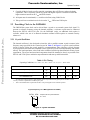
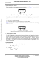
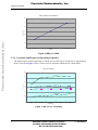
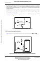
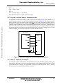
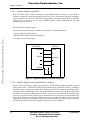
Freescale Semiconductor, Inc.
Freescale
Order by AN1920/D
Freescale Order Number
Rev. 0, 06/2001
Contents
DSP56800 Hardware
Interface Techniques
1. Introduction ....................................1
David Zalac
2. System Functions ...........................1
1.
Introduction
Interface techniques to the DSP56800 Embedded DSP
Controller family of devices are shown. This includes system
interface, memory interface and peripheral interface
examples. This document is intended to cover device
interfacing for the DSP56F801, DSP56F803, DSP56F805,
DSP56F807 and DSP56824 products.
2.
System Functions
In this section, we examine the essential requirements to
power and clock the DSP56800, and address other system
functions including power management, hardware interrupts,
and the processors’ JTAG/OnCE port.
2.1 Providing Supply Voltage to the
DSP56800
The DSP56800 specification for supply voltage is 3.0V
(minimum) to 3.6V (maximum).
2.1 Providing Supply Voltage to the
DSP56800........................................1
2.2 Providing Clock to the DSP56800 ..3
2.3 Power Management.........................4
2.4 Reset/Interrupt Interfaces ................7
2.5 JTAG/OnCE Interface.....................9
3. Memory Interfaces .......................11
3.1 DSP56F800 Memory
Configuration.................................11
3.2 External Memory Interfaces..........14
4. Peripheral Interfaces ....................18
4.1
4.2
4.3
4.4
4.5
4.6
4.7
4.8
GPIO Interface Example ...............18
CAN Interface (DSP56F805)........18
Codec Interface (DSP56824) ........19
PWM Interface ..............................21
Motor Protection Logic .................22
SCI Interface .................................24
Quadrature Decoder Interface .......25
Zero-Crossing Detection ...............25
5. Conclusion ................................... 25
6. References ....................................26
This voltage source is to be applied to the all of the device’s
VDD pins. Internally, this voltage is regulated down to 2.5V
for the core digital circuitry. The analog supply and reference
voltages VDDA and VREF should satisfy the constraints
VREF <= VDDA <= VDD.
The processor supply current is application-dependent and
can be computed using the data supplied in the device’s
Electrical Specification.
An example power supply circuit is given in Figure 1.
© Motorola, Inc., 2001
For More Information On This Product,
Go to: www.freescale.com
DSP56800 Hardware Interface
Techniques
Freescale Semiconductor, Inc...
Semiconductor Application Note
Freescale Semiconductor, Inc.
System Functions
+3.3V
+5.0V
+12V DC
+3.3V
Regulator
+5.0V
Regulator
+3.3V Digital
+3.3V Analog
DSP56F80x
POWER ON
Other System
Parts
Freescale Semiconductor, Inc...
GREEN LED
Figure 1. Schematic Diagram of the Power Supply
The DSP56800 devices include both analog and digital circuitry, making noise control a high priority.
Several design recommendations relating to power, ground and PCB design are given below.
1. All VDD supply pins must be bypassed with a 0.01-0.1µF bypass capacitor (see recommendation
(5) below). The general rule in selecting the capacitor value is to choose the highest value
available in the designer’s selection of capacitor package, although there are more sophisticated
techniques in capacitor-value selection (see Reference 1. in Section 6). The more sophisticated
rules, however, require rather extensive (and typically unavailable) knowledge of output loading
and various characteristics of the user's PCB. The simpler rule follows from the objective of
minimizing capacitor lead inductance by minimizing package size, while ensuring that adequate
electrical charge will be directly available to the processor on a clock-by-clock basis.
Surface-mount capacitors are highly recommended, as these devices have very low-inductance
connections. Inductance of capacitor leads can cause ground bounce, EMI, and signal crosstalk
and degradation.
2. The overall system itself must be bypassed at the power entry point to the PCB with a sufficiently
large capacitor to counteract the inductance of the power supply leads and to be able to deliver
sufficient charge to all bypass capacitors each clock cycle. Recommended is a 100µF tantalum
capacitor.
3. The PCB should be divided into separate sections for analog and digital functions. Ultimately the
analog and digital grounds should be connected at a single -point ground. Additionally, power and
ground planes should be employed in the user’s PCB, minimizing return-path inductance and
isolating digital switching noise from analog circuitry.
4. Provide a low-impedance path from the board power supply to each VDD pin on the DSP, and
from the board ground to each VSS (GND) pin.
5. The minimum bypass requirement is to place 0.01–0.1µF capacitors positioned as closely as
possible to the package supply pins. The recommended bypass configuration is to place one
bypass capacitor on each of the VDD/VSS pairs, including VDDA/VDDSA.
6. Ensure that capacitor leads and associated printed circuit traces that connect to the chip VDD and
VSS (GND) pins are less than 0.5” per capacitor lead.
7. Use at least a four-layer Printed Circuit Board (PCB) with two inner layers for VDD and GND.
8. Because the DSP output signals have fast rise and fall times, PCB trace lengths should be minimal.
2
DSP56800 Hardware Interface Techniques
For More Information On This Product,
Go to: www.freescale.com
Freescale Semiconductor, Inc.
System Functions
9. Consider all device loads as well as parasitic capacitance due to PCB traces when calculating
capacitance. This is especially critical in systems with higher capacitive loads that could create
higher transient currents in the VDD and GND circuits.
10. All inputs must be terminated (i.e., not allowed to float) using CMOS levels.
11. Take special care to minimize noise levels on the V REF, VDDA and VSSA pins.
2.2 Providing Clock to the DSP56800
Freescale Semiconductor, Inc...
The DSP56F80x system clock can be derived from a crystal or an external system clock signal. To
generate a reference frequency using the internal oscillator, a reference crystal must be connected
between the EXTAL and XTAL pins. For the DSP56801 (only), an additional clock option is
available, which is the use of an internal relaxation oscillator which requires no external circuitry
whatsoever.
2.2.1 Crystal Oscillator
The internal oscillator is also designed to interface with a parallel-resonant crystal resonator in the
frequency range specified for the external crystal in Table 1. In Figure 2, a typical crystal oscillator
circuit is shown. Follow the crystal supplier’s recommendations when selecting a crystal, because
crystal parameters determine the component values required to provide maximum stability and reliable
start-up. The load capacitance values used in the oscillator circuit design should include all stray layout
capacitances. The crystal and associated components should be mounted as closely as possible to the
EXTAL and XTAL pins to minimize output distortion and start-up stabilization time.
Table 1: PLL Timing
Operating Conditions: VSS = VSSA = 0 V, VDD = VDDA = 3.0–3.6 V, TA = –40° to +85°C
Characteristic
Symbol
Min
Typ
Max
Unit
External reference crystal frequency for the PLL1
fosc
4
8
8
MHz
PLL output frequency
fop
40
—
80
MHz
PLL stabilization time 2
tplls
—
1
10
ms
1
An externally supplied reference clock should be as free as possible from any phase jitter for the PLL to work
correctly. The PLL is optimized for 8 MHz input crystal.
2
This is the minimum time required after the PLL setup is changed to ensure reliable operation.
Crystal Frequency = 4–8 MHz (optimized for 8 MHz)
EXTAL XTAL
Rz
Sample External Crystal Parameters:
Rz = 10 MΩ
Figure 2. Crystal Oscillator
DSP56800 Hardware Interface Techniques
For More Information On This Product,
Go to: www.freescale.com
3
Freescale Semiconductor, Inc.
System Functions
2.2.2 External Clock Source
The recommended method of connecting an external clock is given in Figure 3. The external clock
source is connected to XTAL and the EXTAL pin is grounded.
DSP56F805
XTAL
EXTAL
External
Clock
GND
Freescale Semiconductor, Inc...
Figure 3. Connecting an External Clock Signal using XTAL
It is possible to instead drive EXTAL with an external clock, though this is not the recommended
method. If you elect to drive EXTAL with an external clock source, the following conditions must be
met:
1. XTAL must be completely unloaded
2. The maximum frequency of the applied clock must be less than 8MHz
Figure 4 illustrates how to connect an external clock circuit with a external clock source using
EXTAL as the input.
DSP56F805
XTAL
EXTAL
External
No
Connection Clock ( < 8MHz)
Figure 4. Connecting an External Clock Signal using EXTAL
2.3 Power Management
The DSP56F80x power requirement depends on several factors, including mode of operation
(ACTIVE, STOP or WAIT), and system-level parameters including supply voltage, clock frequency,
operating temperature and output loading. Careful consideration of each of these factors can result in a
supply current requirement significantly less that the maximum found in the device Electrical
Specification. In the following sub-sections, plots are shown that apply only to the DSP56F805. These
are intended to show behavior of the device current requirement and do not supersede the device
Electrical Specification.
2.3.1 Device Model
The DSP56800 total current requirement (Itotal) is given by:
Itotal = Idigital + Ianalog
Idigital is given by:
Idigital = C*VDD*f
4
DSP56800 Hardware Interface Techniques
For More Information On This Product,
Go to: www.freescale.com
Freescale Semiconductor, Inc.
System Functions
where C depends on die area and output capacitive loading as described below, VDD is the digital
supply voltage, and f is the operating frequency of the device. This results from a total capacitance C
being charged every T seconds, where T is the machine cycle time. The charge required from the
power supply for each cycle T is Q = C * VDD. Hence Idigital = Q/T = C * VDD * f. Further, Idigital
varies with temperature as described in subsequent sections.
Ianalog depends on output loading and other factors as described below.
Freescale Semiconductor, Inc...
2.3.2 Mode of Operation
The DSP56800 devices support two low-power modes, referred to as STOP and WAIT modes. These
are described in detail in the associated device User Manuals, and the resulting reductions in supply
current requirement are given in the device Electrical Specifications. Both modes put the CPU to sleep.
The PLL and peripheral bus continue to run in WAIT mode, but not in STOP mode. The ADC is
placed in a low-power mode in both cases.
2.3.3 Variation with Respect to Supply Voltage
The digital supply current requirement of CMOS devices with respect to supply voltage is
approximately linear, as shown in Figure 5. below for the DSP56805. The DSP56800 devices possess
both a CMOS current requirement and an analog current requirement. The variation of analog supply
current with respect to analog supply voltage is shown in Figure 6. These curves are consistent with
the model described in Section 2.3.1.
Total IDD vs VDD (nom Temp, 80 MHz PLL)
92
90
88
86
84
82
80
78
76
74
72
VDD min
VDD nom
VDD max
VDD
Figure 5. Total IDD vs. VDD
DSP56800 Hardware Interface Techniques
For More Information On This Product,
Go to: www.freescale.com
5
Freescale Semiconductor, Inc.
System Functions
IDDA vs. VDDA (nom Temp, 80 MHz PLL)
55.5
55
54.5
54
Freescale Semiconductor, Inc...
53.5
53
52.5
52
VDDA min
VDDA nom
VDDA max
VDDA
Figure 6. IDDA vs. VDDA
2.3.4 Variation with Respect to Operating Frequency
The digital supply current requirement of CMOS devices with respect to frequency is approximately
linear, as shown in Figure 7 below. These curves are consistent with the device current model.
IDD vs. PLL Frequency
120
IO IDD max
100
80
Analog IDD max
60
Analog IDD typical
40
IO IDD typical
20
0
0 MHz
20 Mhz
40 Mhz
60 Mhz
80 Mhz
PLL Frequency
Figure 7. IDD vs. PLL Frequency
6
DSP56800 Hardware Interface Techniques
For More Information On This Product,
Go to: www.freescale.com
Freescale Semiconductor, Inc.
System Functions
2.3.5 Variation with Respect to Output Loading
Output loading influences supply current requirement in a manner similar to that described by the
model given in Section 2.3.1. Output load current for a given output pin is the sum of DC and AC
currents. The DC current requirement is that imposed by connected devices, such as TTL inputs. The
AC component is essentially a time-averaged capacitor charging current, which is dependent on VDD,
capacitance and switching frequency. The capacitance in this case is the sum of DSP56800 output
buffer capacitance, input capacitances of connected CMOS or other devices, and trace and stray
capacitances.
Freescale Semiconductor, Inc...
2.3.6 Power Dissipation
Minimization of power dissipation of the DSP56800 device is a slightly different problem than that of
minimizing the device’s supply current requirement. The chief difference lies in the way the I/O pins
of the device are exercised. For example, when a DSP56800 digital I/O pin sinks current, the internal
energy generated must be dissipated as heat, although literally this does not affect the DSP56800’s
current requirement, because this current does not enter the device through its VDD pins.
The specification of power dissipation for a given DSP56800 device is given in the corresponding data
sheet.
2.4 Reset/Interrupt Interfaces
2.4.1 Sources of Reset
The following sources of reset are present in this example system:
•
Power-On Reset (POR)
•
External Reset
•
Computer Operating Properly (COP) Reset
Figure 8 illustrates how these RESET sources are used within the chip.
COP
(active low)
COP RESET
Delay
pulse shaper
CORE
External
RESET IN
(active low)
Hardware RESET
Delay
Power on
Reset
res
ires
pulse shaper
system reset
Figure 8. Sources of RESET
DSP56800 Hardware Interface Techniques
For More Information On This Product,
Go to: www.freescale.com
7
Freescale Semiconductor, Inc.
System Functions
By default, the pulse shaper functions force internal reset signals to be a minimum of 32 oscillator
clock cycles long. 38T (where T = 1/2 cycle) is required for the DSP56800 core and 1µs is required for
recovery time for the embedded flash. So, 32 works out to be a convenient value (assuming 8MHz
oscillator frequency).
In addition to the reset sources above, two low-voltage detect signals may be used to initiate a
controlled shutdown of the chip when the supply drops below acceptable levels. These low-voltage
detect circuits are set up as high-priority interrupts. They can be masked if desired. See Chapter 16 in
the DSP56F80x User’s Manual.
Logic is provided on the DSP56800 to generate a clean power-on RESET signal. An example RESET
circuit is shown in Figure 9.
Freescale Semiconductor, Inc...
+3.3V
RESET
PUSHBUTTON
MANUAL RESET
RESET
P_RESET
Figure 9. Schematic Diagram of the RESET Interface
2.4.2 External Interrupt Pin Interface
Figure 10 shows an example hardware interface to the external interrupt pins IRQA and IRQB.
+3.3V
DSP56F807
10K
SW2
IRQA
0.1µF
+3.3V
10K
SW3
IRQB
0.1µF
Figure 10. Schematic Diagram of the External Interrupt Pin Interface
8
DSP56800 Hardware Interface Techniques
For More Information On This Product,
Go to: www.freescale.com
Freescale Semiconductor, Inc.
System Functions
2.4.3 GPIO Pin Configured as Interrupt Interface
An example interface to GPIO pins found on the DSP56800 device is shown in Figure 11. These
inputs can be configured as interrupt sources or as general-purpose I/O’s as described further in the
device User’s Manuals.
+3.3V
DSP56F807
10K
GP #1 SWITCH
PD3
Freescale Semiconductor, Inc...
+3.3V
GP #2 SWITCH
10K
PD4
+3.3V
START/STOP SWITCH
10K
PD5
Figure 11. Run/Stop and General Purpose Switches
2.5 JTAG/OnCE Interface
Figure 12 shows a parallel interface to the DSP56800 JTAG/OnCE port. When using the parallel
JTAG interface, the jumper should be removed. Further information on the OnCE port follows.
Parallel JTAG Interface
DB-25 Connector
TDI
TDO
P_TRST
TMS
TCK
P_RESET
+3.3V
JG4
Jumper Removed:
Enable JTAG I/F
DSP56F800
IN OUT
OUT IN
IN OUT
IN OUT
IN OUT
TDI
TDO
TRST
TMS
TCK
IN
RESET
OUT
EN
1
2
Jumper Pin 1-2:
Disable JTAG I/F
Figure 12. Block Diagram of the Parallel JTAG Interface
DSP56800 Hardware Interface Techniques
For More Information On This Product,
Go to: www.freescale.com
9
Freescale Semiconductor, Inc.
System Functions
This section is dedicated to testing and debugging retention, but specifically through the Joint Test
Action Group, (JTAG) and the OnCE module.
DSP56F801/803/805/807 provides board and chip-level testing capability through two on-chip
modules, both accessed through the JTAG port/OnCE module interface:
•
On-chip Emulation (OnCE) module
•
Test Access Port (TAP) and 16-state controller, also known as the Joint Test Action Group
(JTAG) port
Presence of the JTAG port/OnCE module interface permits insertion of the DSP chip into a target
system while retaining debug control. This capability is especially important for devices without an
external bus, because it eliminates the need for a costly cable to bring out the footprint of the chip
required by a traditional emulator system.
Freescale Semiconductor, Inc...
The OnCE module is a Freescale-designed module used in Digital Signal Processor (DSP) chips to
debug application software employed with the chip. The port is a separate on-chip block allowing
non-intrusive DSP interaction with accessibility through the pins of the JTAG interface. The OnCE
module makes it possible to examine registers, memory, or on-chip peripherals’ contents in a special
debug environment. This avoids sacrificing any user-accessible on-chip resources to perform
debugging. See Chapter 17, OnCE Module, in the DSP56F80x User’s Manual for details on the
OnCE module implementation of the DSP56F801,803, 805 and 807 series.
The JTAG port is a dedicated user-accessible TAP compatible with the IEEE 1149.1a-1993 Standard
Test Access Port and Boundary Scan Architecture. Problems associated with testing high-density
circuit boards have led to the development of this proposed standard under the sponsorship of the Test
Technology Committee of IEEE and the JTAG. DSP56F 801 through 807 supports circuit board test
strategies based on this standard.
Five dedicated pins interface to the TAP containing a 16-state controller. The TAP uses a boundary
scan technique to test the interconnections between integrated circuits after they are assembled onto a
Printed Circuit Board (PCB). Boundary scans allow a tester to observe and control signal levels at
each component pin through a shift register placed next to each pin. This is important for testing
continuity and determining if pins are stuck at a one or zero level.
Features of the TAP port include the following:
10
•
Perform boundary scan operations to test circuit board electrical continuity
•
Bypass the DSP for a given circuit board test by replacing the Boundary Scan Register (BSR)
with a single-bit register
•
Sample the DSP system pins during operation and transparently shift out the result in the CSR;
pre-load values to output pins prior to invoking the EXTEST instruction
•
Disable the output drive to pins during circuit board testing
•
Provide a means of accessing the OnCE module controller and circuits to control a target
system
•
Query identification information, manufacturer, pat number, and version from a DSP chip
•
Force test data onto the outputs of a DSP IC while replacing its BSR in the serial data path
with a single bit register
•
Enable a weak pull-up current device on all input signals of a DSP IC, helping to assure
deterministic test results in the presence of continuity fault during interconnect testing
DSP56800 Hardware Interface Techniques
For More Information On This Product,
Go to: www.freescale.com
Freescale Semiconductor, Inc.
Memory Interfaces
This section includes aspects of the JTAG implementation specific to the DSP56F801 through 807.
This data is intended to be utilized with IEEE 1149.1a. The discussion includes those items required
by the standard to be defined and, in certain cases, provides additional information specific to the
DSP56F801/803/805/807. For internal details and applications of the standard, refer to IEEE 1149.1a.
3.
Memory Interfaces
Freescale Semiconductor, Inc...
Memory configuration is controlled slightly differently for the DSP56800 and DSP5682x devices as
described below. From a hardware perspective, the DSP56800 device memory map is controlled by a
single pin (EXTBOOT), while for DSP5682x devices, the MODA and MODB pins control the
memory configuration.
3.1 DSP56F800 Memory Configuration
The DSP56800 chips have two valid operating modes determining the memory maps for program
memory. Operating modes can be selected either by applying the appropriate signal to the EXTBOOT
pin during reset, or by writing to the Operating Mode Register (OMR) and changing the MA and MB
bits.
Table 2: DSP56800 Program Memory Chip Operating Modes
State of EXTBOOT upon reset
MB
MA
Chip operating mode
0
0
0
Mode 0
NORMAL Operation
N/A
0
1
NOT SUPPORTED
N/A
1
0
1
1
1
Mode 3
EXTERNAL ROM
The EXTBOOT pin is sampled as the chip leaves the reset state, and the initial operating mode of the
chip is set accordingly.
Chip operating modes can also be changed by writing to the operating mode bits MB and MA in the
OMR. Changing operating modes does not reset the chip. Interrupts should be disabled immediately
before changing the OMR. This will prevent an interrupt from going to the wrong memory location.
Also, one No-Operation (NOP) instruction should be included after changing the OMR to allow for
re-mapping to occur.
Note:
Upon Computer Operating Properly (COP) reset, the MA and MB bits will revert to the values
originally latched from the EXTBOOT pin in contradiction of RESET, hardware reset. These
original mode values determine the COP reset vector.
3.1.1 Single Chip Mode: Start-up (Mode 0)
Mode zero is the single-chip mode. Internal Program RAM (PRAM) and PFLASH are enabled for
reads and fetches. The DSP56xxx have two sub-modes for:
1. Mode 0A, boot mode, where all memory is internal
2. Mode 0B, non-boot mode, where the first 32K of memory is internal and the second 32K is
external
DSP56800 Hardware Interface Techniques
For More Information On This Product,
Go to: www.freescale.com
11
Freescale Semiconductor, Inc.
Memory Interfaces
If EXTBOOT is asserted low during reset, then Mode 0A: boot is automatically entered when exiting
Reset mode.
For DSP56F801, Mode0B is not supported because there is no external memory interface.
Note:
Locations zero through three in the program memory space are actually mapped to the first
four locations in the Boot Flash.
Mode zero is useful to enter when coming out of reset for applications while executing primarily from
internal program memory. The reset vector location in Modes zero and three is located in the program
memory space at location P:$0000, P:$0002 for COP timer reset. For Mode zero, this is in internal
program memory. In Mode three, it is in off-chip program memory.
Freescale Semiconductor, Inc...
3.1.2 Modes 1 & 2
Modes one and two are NOT SUPPORTED for these parts. They are used for ROM-based members of
the DSP56800 family.
3.1.3 External Mode (Mode 3)
Mode three is a development mode in which the entire 64K program memory space is external. No
internal program memory may be accessed, except as a secondary read of Data RAM. The reset vector
location in Mode three is located in the external program memory space at location P:$0000, P:$0002
for COP timer reset.
3.1.4 DSP56824 Memory Configuration
The DSP56824 has four operating modes that determine the memory maps for program and data
memories and the startup procedure when the chip leaves the Reset state. Operating modes can be
selected either by applying the appropriate signals to the MODA and MODB pins during reset, or by
writing to the OMR and changing the MA and MB bits, as shown in Table 2.
.
Table 3: DSP56824 Program RAM Chip Operating Modes
Program Memory Configuration
MB or
MODB
Value
MA or
MODA
Value
0
0
Mode 0
Single Chip
Startup
Internal program ROM
P:$0000 or P:$0002
(COP reset)
Read/fetch: internal program ROM
Write: internal program
RAM
All accesses:
internal program
ROM
0
1
Mode 1
Single Chip
User
Internal program ROM
P:$7F80 or P:$7F82
(COP reset)
All accesses: internal program RAM
All accesses:
internal program
ROM
1
0
Mode 2
Normal
Expanded
External program
memory P:$E000 or
P:$E002
(COP reset)
Read/fetch: internal program ROM
Write: internal program
RAM
All accesses:
internal program
ROM
1
1
Mode 3
Development
External program
memory P:$0000 or
P:$0002
(COP reset)
All accesses: external
program memory
All accesses:
external program memory
12
Chip
Operating
Mode
Reset Vector
P:$7F–$0
DSP56800 Hardware Interface Techniques
For More Information On This Product,
Go to: www.freescale.com
P:$8000–$80
Freescale Semiconductor, Inc.
Memory Interfaces
The MODA and MODB pins are sampled as the DSP56824 leaves the Reset state, and the initial
operating mode of the chip is set accordingly. After the Reset state is exited, the MODA and MODB
pins become interrupt pins, IRQA and IRQB. One of four initial operating modes is selected, based on
the values detected on MODA and MODB:
•
Single Chip mode (Mode 0 or Mode 1)
•
Normal Expanded mode (Mode 2)
•
Development mode (Mode 3)
Freescale Semiconductor, Inc...
Chip operating modes can also be changed by writing to the MB and MA bits in the OMR. Changing
operating modes does not reset the DSP56824. To prevent an interrupt from going to the wrong
memory location, interrupts should be disabled immediately before changing the OMR. Also, one
no-operation (NOP) instruction should be included after changing the OMR to allow for remapping to
occur.
Note:
On a Computer Operating Properly (COP) reset, the MA and MB bits (in the OMR) revert to
the values originally latched from the MODA and MODB pins on deassertion of RESET.
These values determine the COP reset vector. For example, if the DSP56xxx left hardware
reset in Mode 2 and the mode bits in the OMR were later changed to specify Mode 3, a COP
reset would use reset vector P:$E002 (for Mode 2) for its reset vector, and not P:$0002 (for
Mode 3).
3.1.5 Single Chip Bootstrap Mode (Mode 0)
Mode 0 is the Single Chip bootstrap mode in which all the internal program and data memory space is
enabled; see Table 3. Mode 0 can be entered by either pulling the MODA and MODB pins low before
resetting the chip or by writing to the OMR and clearing the MA and MB bits. Writes to the lower 128
words of internal program space will write to the internal program RAM. The reset vector location in
Mode 0 is P:$0000 in the internal program ROM (P:$0002 for COP timer reset).
Mode 0 is useful when exiting the Reset state for applications that execute primarily from internal
program ROM. Write access to the internal program RAM allows an application to copy interrupt
vectors and program code from program ROM to identically addressed locations in program RAM
without changing operating modes.
3.1.6 Single Chip User (Mode 1)
Mode 1 is the Single Chip user mode in which 34,640 (32,768 – 128) words of internal program ROM
are enabled for reads and fetches. All accesses to the lower 128 words of internal program space are to
the internal program RAM. The reset vector location in Mode 1 is P:$7F80 in the internal program
ROM (P:$7F82 for COP timer reset). The user should observe that these reset vectors are located in the
area reserved for the bootstrap program.
Mode 1 is the ordinary user mode for applications that execute primarily from internal program ROM
or for applications that must access the internal program RAM. The internal program RAM is typically
loaded in Mode 0 or by the bootstrap program in Mode 1. For more information on loading the internal
program RAM in this manner, see Appendix A, “Bootstrap Program”, in the DSP56824 User’s
Manual.
DSP56800 Hardware Interface Techniques
For More Information On This Product,
Go to: www.freescale.com
13
Freescale Semiconductor, Inc.
Memory Interfaces
3.1.7 Normal Expanded Mode (Mode 2)
In the Normal Expanded mode (Mode 2), all 32,768 words of internal program ROM are enabled for
reads and fetches. Writes to the lower 128 words of internal program space will write to the internal
program RAM. The reset vector location in Mode 2 is at P:$E000 in the external program RAM
(P:$E002 for COP timer reset).
Mode 2 is identical to Mode 0 except that the reset vectors are in external memory. This feature
provides additional flexibility for application development.
Freescale Semiconductor, Inc...
3.1.8 Development Mode (Mode 3)
Mode 3 is the Development mode, in which the entire 65,536 words of program memory space is
external. No internal program memory space can be accessed. The reset vector location in Mode 3 is at
P:$0000 in the external program memory space (P:$0002 for COP timer reset). Mode 3 is the primary
mode for application development on the DSP56824.
3.2 External Memory Interfaces
The DSP56800 family devices (excluding the DSP56801) have an external 16-bit multiplexed data bus
that can be used for program word or data accesses to memory devices, including ROM, FLASH,
EEPROM, or SRAM. The PS and DS outputs from the DSP device differentiate the two types of
accesses. External bus accesses are referred to as asynchronous, as the timing specifications given in
the appropriate Electrical Specifications for each device are not made with respect to the DSP clock.
3.2.1 Wait State Management for the DSP56800
Optimization of external memory use, particularly for DSP56800 devices, depends on several factors
that can be taken into consideration for a given hardware design.
First, as much internal memory as possible for a given application should be used, as all internal
accesses require zero wait states.
Second, if external memory must be used, partitioning the total code into two pieces can be beneficial.
These two pieces are i) often used and repeated code, and ii) code used or needed less frequently.
Third, wait states (WS) are programmable for the values 0, 4, 8 and 12. Wait states have traditionally
provided a means for accessing slower memories motivated either by technology limitations or to the
cost advantage offered by slower memory devices. Each wait state extends external bus accesses by
2*WS clock periods. Note that wait state values are independently programmable for external X (data)
memory and external program memory. For example, the clock period (Top) for a device running at
80MHz (CPU clock of 40MHz) is 12.5ns. External memory access time is given by :
tACC = Top*WS + (Top-11.5) (ns)
For example, 4 wait states for a CPU running at 40MHz (clock rate of 80MHz) results in a memory
access time of 12.5*4 + (12.5-11.5) = 51ns.
Many modern memory devices, such as SRAMs, cannot operate with 0 wait states but can, however,
be accessed in the sub-10ns range. Therefore, for certain applications, it is worthwhile to consider
selecting a lower clock frequency in order to be able to access external memory with no wait states.
This is particularly true of applications that must make heavy use of external memory and is
exemplified by the following:
Suppose an application requires only 25MIPS, rather than the maximum of 40MIPS.
14
DSP56800 Hardware Interface Techniques
For More Information On This Product,
Go to: www.freescale.com
Freescale Semiconductor, Inc.
Memory Interfaces
Then:
Top = 1/50e6 = 20ns
WS = 0
tACC = Top*0 + (Top – 11.5) = 8.5ns
Many SRAM devices are available in this speed range.
Freescale Semiconductor, Inc...
3.2.2 Program and Data Memory Example Interface
The DSP56807 EVM uses one bank of 128K×16-bit Fast Static RAM (GSI GS72116, labelled U2) for
external memory expansion; see the FSRAM schematic diagram in Figure 13. This physical memory
bank is split into two logical memory banks of 64Kx16-bits: one for program memory and the other for
data memory. By using the DSP’s program strobe, PS, signal line along with the memory chip’s A0
signal line, half of the memory chip is selected when program memory accesses are requested and the
other half of the memory chip is selected when data memory access are requested. This memory bank
will operate with zero wait state accesses while the DSP56F807 is running at 70MHz. However, when
running at 80MHz, the memory bank operates with four wait state accesses.
GS72116
DSP56F807
A0-A15
A1-A16
PS
A0
D0-D15
DQ0-DQ15
RD
OE
WR
WE
+3.3V
JG1
CE
Figure 13. Schematic Diagram of the External Memory Interface
3.2.3 Memory Expansion Techniques
The total memory space addressable by the DSP56800 device is 64K words for program memory, plus
64K words for data memory. However, paging techniques can be implemented in hardware as shown
in the following two examples. The application developer must take appropriate steps in software
development to accommodate page boundary transitions.
DSP56800 Hardware Interface Techniques
For More Information On This Product,
Go to: www.freescale.com
15
Freescale Semiconductor, Inc.
Memory Interfaces
3.2.3.1 Memory Paging Using GPIO
Figure 14 below shows a simple technique to select different banks of memory. A given bank of
memory is enabled by setting the appropriate GPIO pin to zero. Note that only one bank of memory
can be enabled at any given time. Therefore, the programmer must manage the GPIO pins carefully,
allowing only one pin to be set low in the expanded memory system. Pseudocode for using this
technique is given as follows.
Initialize GPIO pin control registers
For a page transition (indicated by software monitoring or by an interrupt handler):
Freescale Semiconductor, Inc...
i) Jump to internal program memory
ii) Modify GPIO control registers as appropriate
iii) Jump to the new external page
GS72116
DSP56F807
A0-A15
A1-A16
PS
A0
D0-D15
DQ0-DQ15
RD
OE
WR
WE
+3.3V
GPIOBn
2.5K
CE
Figure 14. Expansion Memory Example Using GPIO
3.2.3.2 Memory Paging Using Latched Data as Address
Figure 15 shows a second way to page external memory. This technique multiplies the address space to
8 times 64K words = 512K words of both program and data space. Each memory bank is selected by
an output from the ‘138 decoder. The decoder’s inputs are driven from 3 outputs of a 4-bit latch, fed by
3 data lines from the DSP56800 device. A dedicated GPIO pin controls the clock to the latch. When
the GPIO pin is set high, the latch cannot be written. To execute a page transition, the GPIO pin must
be set low via software control, followed by an external data write to the latch. The page must then be
locked in in software by setting the GPIO pin back to one. Further, the GPIO pin can be used in
conjuction with other logic to disable writing of any other external devices during a page transition.
The following summarizes the steps required in software to use this technique.
16
DSP56800 Hardware Interface Techniques
For More Information On This Product,
Go to: www.freescale.com
Freescale Semiconductor, Inc.
Memory Interfaces
Initialize GPIO control registers
For a page transition:
i) Set GPIO to zero
ii) Execute external write cycle to latch with 12 waitstates
iii) Set GPIO to one
Note that one address of each bank must be reserved, as the write cycle to the latch will also write the
corresponding address in the previously selected bank.
DSP56F807
Freescale Semiconductor, Inc...
GS72116
74LS138
3
D0-D2
4-bit
Latch
A0
CE
3
3-8 Decoder
OE
GS72116
A0
CE
WR
GPIOB0
PS
Figure 15. Expansion Memory
DSP56800 Hardware Interface Techniques
For More Information On This Product,
Go to: www.freescale.com
17
Freescale Semiconductor, Inc.
Peripheral Interfaces
4.
Peripheral Interfaces
The following sections provide example interfaces to DSP56800 peripherals. The interfaces have been
implemented and tested on Evaluation Module (EVM) hardware using various members of the
DSP56800 family.
4.1 GPIO Interface Example
An example interface making use of the DSP56800 GPIO pins is given below. The GPIO pins are
controllable via SDK driver routines. Refer to the SDK Programmer’s Guide for details.
Freescale Semiconductor, Inc...
Two general-purpose user pushbutton switches are connected to Port D GPIO signals GPIOB0 and
GPIOB1. A Run/Stop toggle switch is connected to GPIO signal GPIOB2; see Figure 16.
+3.3V
DSP56F807
10K
GP #1 SWITCH
GPIOB0
+3.3V
GP #2 SWITCH
10K
GPIOB1
+3.3V
START/STOP SWITCH
10K
GPIOB2
Figure 16. Run/Stop and General Purpose Switches
4.2 CAN Interface (DSP56F805)
The DSP56F805EVM board contains a CAN physical-layer interface chip that is attached to the
MSCAN_RX and MSCAN_TX pins on the DSP56F805. The EVM board uses a Philips, PCA82C250,
high speed, 1Mbps, physical layer interface chip. Due to the +5.0V operating voltage of the CAN chip,
a pull-up to +5.0V is required to level shift the Transmit Data output line from the DSP56F805. A
primary, J1, and a daisy-chain, J2, CAN connector are provided to allow easy daisy-chaining of CAN
devices. CAN bus termination of 120 ohms can be provided by adding a jumper as shown. Refer to
Figure 4 for the CAN connector signals and Figure 17 for a connection diagram.
18
DSP56800 Hardware Interface Techniques
For More Information On This Product,
Go to: www.freescale.com
Freescale Semiconductor, Inc.
Peripheral Interfaces
CAN CONNECTOR
J1
1
3
5
7
X
DSP56F805
+5.0V
X
X
U20
MSCAN_TX
1
MSCAN_RX
4
8
2
4
6
8
X
X
X
X
3
VCC
5
VREF
TXD
RXD
CANH
CANL
SLOPE
GND
7
6
1
2
120
2
PCA82C250T
Freescale Semiconductor, Inc...
CAN TERMINATION
X
X
X
J2
1
3
5
7
2
4
6
8
X
X
X
X
DAISY-CHAIN
CAN CONNECTOR
Figure 17. CAN Interface
Table 4: CAN Header Description
J1 and J2
Pin #
Signal
Pin #
Signal
1
NC
2
NC
3
CANL
4
CANH
5
GND
6
NC
7
NC
8
NC
9
NC
10
NC
4.3 Codec Interface (DSP56824)
The DSP56824EVM provides a 13-bit linear single-channel CODEC (Freescale MC145483,
designated as U10). The DSP56824 interfaces to the CODEC via the DSP’s Synchronous Serial
Interface (SSI) through the SSI enable connector, J1. This connector allows the SSI Port to either
control the on-board SSI CODEC or to control an off-board SSI device. Table 5 lists the J1 pin-outs.
The SSI port provides the CODEC’s clock, frame synchronization and data without the use of glue
logic; see Figure 18.
DSP56800 Hardware Interface Techniques
For More Information On This Product,
Go to: www.freescale.com
19
Freescale Semiconductor, Inc.
Peripheral Interfaces
CODEC Enable
(SSI Port Connector)
DSP56824
MC145483
J1
STD
DR
SRD
DT
STCK
BCLKR, BCLKT, MCLK
FST, FSR
STFS
SRCK
Freescale Semiconductor, Inc...
SRFS
Figure 18. Block Diagram of the SSI CODEC Interface
Table 5: SSI CODEC Enable Connector Descriptor
J1
Pin #
DSP Signal
Pin #
CODEC Signal
1
STD/PC8
2
DR
3
SRD/PC9
4
DT
5
STCK/PC10
6
BCLKR/BCLKT/MCLK
7
STFS/PC11
8
FST/FSR
9
SRCK/PC12
10
NC
11
SRFS/PC13
12
NC
13
GND
14
GND
3.4 DAC Interface using SPI Port
The DSP56F807EVM board contains a serial 10-bit, 4-channel D/A converter connected to the
DSP56F807’s SPI port. The output pins are uncommitted and are connected to a 4X2 header, J1, to
allow easy user connections. Refer to Figure 19 for the D/A connections. The D/A’s output full-scale
range value can be set to a value from 0.0V to 2.4V by a trimpot, R1. This trimpot is preset to +2.05V,
which provides approximately 2mV per step.
20
DSP56800 Hardware Interface Techniques
For More Information On This Product,
Go to: www.freescale.com
Freescale Semiconductor, Inc.
Peripheral Interfaces
DSP56F807
MAX5251
MOSI
J1
DIN
MISO
DOUT
SCLK
SCLK
OUT A
OUT B
OUT C
OUT D
PB4
CS
RSTO
CL
D/A CONNECTOR
D/A 0
D/A 1
D/A 2
D/A 3
1
2
3
4
5
6
7
8
Vref
R1
+3.3VA
Freescale Semiconductor, Inc...
10K
Figure 19. Serial 10-bit, 4-Channel D/A Converter
4.4 PWM Interface
The sections below describe example interfaces to the PWM module(s) available on DSP56800
devices.
The DSP56F807 has two independent groups of dedicated PWM units. Each unit contains six PWM,
three Phase Current sense and four Fault input lines. PWM group A’s PWM lines are connected to a
UNI-3 interface connector and to a set of six PWM LEDs via inverting buffers. “UNI-3” refers to a
Freescale-defined parallel interface. Typically, any parallel cable, such as a HDD cable, will satisfy the
requirements of the DSP56800 device. The inverting buffers are used to isolate and drive the DSP’s
PWM group A’s outputs to the PWM LEDs. The PWM LEDs indicate the status of PWM group A
signals, as shown in Figure 20.
DSP56F807
UNI-3
PWMA0
PWMA1
PWMA2
PWMA3
PWMA4
PWMA5
+3.3V
PWMA0
PWMA1
PWMA2
PWMA3
PWMA4
PWMA5
LED4
YELLOW LED
PHASE A TOP
LED5
GREEN LED
LED
BUFFER
PHASE A BOTTOM
LED6
YELLOW LED
PHASE B TOP
LED7
GREEN LED
PHASE B BOTTOM
LED8
YELLOW LED
PHASE C TOP
LED9
GREEN LED
PHASE C BOTTOM
Figure 20. PWM Group A Interface and LEDs
DSP56800 Hardware Interface Techniques
For More Information On This Product,
Go to: www.freescale.com
21
Freescale Semiconductor, Inc.
Peripheral Interfaces
4.5 Motor Protection Logic
The DSP56F807EVM contains two UNI-3 connectors that interface with various motor drive boards,
Primary UNI-3 and Secondary UNI-3. The DSP can sense error conditions generated by the motor
power stage boards via signals on the UNI-3 connector. The motor driver board’s Motor Supply DC
Bus Voltage, Current and Motor Phase Currents are sensed on a separate power stage board. The
conditioned signals are transferred to the DSP board via the UNI-3 connector. These analog input
signals are compared to a limit set by trimpots. If the input analog signals are greater than the limit set
by the trimpot, a DSP digital voltage-compatible +3.3V DC fault signal is generated.
4.5.1 Primary UNI-3 Motor Protection Logic
Freescale Semiconductor, Inc...
The Primary UNI-3 DC Bus Over-Voltage signal is connected to the DSP’s PWM group A fault
inputs. The three Primary UNI-3 Phase Over-Current signals are connected to the DSP’s PWM group
A’s fault inputs, i.e., FAULTA1, FAULTA2 and FAULTA3. Figure 22 contains the diagram of the
Over-Voltage and one phase of the Phase Over-Current circuit for the UNI-3 interface. The FAULTA1
input can be sourced from the Phase A Over-Current circuit or the DC Bus Over-Current circuit.
Jumper JG1 provides the selection; reference Figure 21 and Table 6.
DC BUS CURRENT SENSE
I_sense_DCB
+3.3V
+5.0V
+5.0V
+
–
LM393
+5.0V
JG1
3
2
1
FAULTA1
+3.3V
+5.0V
PHASE A CURRENT SENSE
PHA_IS
+
–
LM393
Figure 21. FAULTA1 Selection Circuit
22
DSP56800 Hardware Interface Techniques
For More Information On This Product,
Go to: www.freescale.com
Freescale Semiconductor, Inc.
Peripheral Interfaces
Table 6: FAULTA1 Source Selection Jumper
JG1
Comment
1–2
Phase A Over-Current Sense input
2–3
DC Bus Over-Current Sense input
DC BUS VOLTAGE SENSE
V_sense_DCB
Freescale Semiconductor, Inc...
+3.3V
+5.0V
+5.0V
+
FAULT0
–
LM393
EXAMPLE DC PHASE CURRENT SENSE
+5.0V
+3.3V
+5.0V
+
FAULT2
PHB_IS
–
LM393
Figure 22. DC-Bus Over-Voltage and Phase Over-Current Detection Circuits
DSP56800 Hardware Interface Techniques
For More Information On This Product,
Go to: www.freescale.com
23
Freescale Semiconductor, Inc.
Peripheral Interfaces
4.6 SCI Interface
An example of an SCI interface is that provided by the DSP56F807EVM. The EVM provides an
RS-232 interface by the use of an RS-232 level converter, (Maxim MAX3245EEAI). Refer to the
RS-232 schematic diagram in Figure 23. The RS-232 level converter transitions the SCI UART’s
3.3V signal levels to RS-232 compatible signal levels and connects to the host’s serial port via
connector P3. Flow control is not provided, but could be implemented using uncommitted GPIO
signals. The pinout of connector P3 is listed in Table 7. The RS-232 level converter/transceiver can be
disabled by placing a jumper at JG1.
RS-232
Level Converter
Interface
Freescale Semiconductor, Inc...
DSP56F807
1
6
TXDO
T1in
RXDO
R1out
T1out
2
R1in
3
7
8
+3.3V
x
FORCEOFF
Jumper Removed:
Enable RS-232
Jumper Pin 1-2:
Disable RS-232
4
9
5
JG1
1
2
Figure 23. Schematic Diagram of the RS-232 Interface
.
Table 7: RS-232 Serial Connector Description
P3
24
Pin #
Signal
Pin #
Signal
1
Jumper to 6 & 4
6
Jumper to 1 & 4
2
TXD
7
Jumper to 8
3
RXD
8
Jumper to 7
4
Jumper to 1 & 6
9
N/C
5
GND
DSP56800 Hardware Interface Techniques
For More Information On This Product,
Go to: www.freescale.com
Freescale Semiconductor, Inc.
Conclusion
4.7 Quadrature Decoder Interface
The DSP56F807EVM board contains a Primary and Secondary Quadrature Encoder/Hall-Effect
interface connected to the DSP’s first and second Quad Encoder input ports. The circuit is designed to
accept +3.0V to +5.0V encoder or Hall-Effect sensor inputs. Input noise filtering is supplied on the
input path for the Quadrature Encoder/Hall-Effect interface, along with additional noise rejection
circuitry inside the DSP. Figure 24 contains the primary encoder interface. The secondary encoder
interface is a duplicate of the primary encoder interface.
Freescale Semiconductor, Inc...
4.8 Zero-Crossing Detection
An attached UNI-3 motor drive board contains logic that can send out pulses when the phase voltage
of an attached 3-phase motor drops to zero. The motor drive board circuits generate a 0 to +5.0V DC
pulse via voltage comparators. The resulting pulse signals are sent to a set of jumper blocks shared
with the Encoder/Hall-Effect interface. The jumper blocks allow the selection of Zero-Crossing signals
or Quadrature Encoder/Hall-Effect signals. When in operation, the DSP will only monitor one set of
signals, Encoder/Hall-Effect or Zero-Crossing. Figure 24 contains the Zero-Crossing and
Encoder/Hall circuits.
ZERO_X_A
DSP56F807
ZERO_X_B
JG12
1
ZERO_X_C
2
PHASEA1
5
PHASEB1
8
INDEX1
3
FILTER
+5.0V
4
6
1
2
3
4
5
6
PIN 1:
PIN 2:
PIN 3:
PIN 4:
PIN 5:
PIN 6:
FILTER
FILTER
7
9
+5.0V
GROUND
PHASE A
PHASE B
INDEX
HOME
FILTER
HOME 1
Figure 24. Zero-Crossing Encoder Interface
5.
Conclusion
In this document, we have examined DSP56800 device hardware interfaces, including those
supporting system functions, external memory, and device peripherals. With respect to each of these
categories of interfaces, we have seen that the sophistication of the DSP56800 device translates into
numerous ways in which to interface it to the rest of a system. For example, multiple clocking modes,
versatile memory access aided by software-programmable wait states and memory extension
techniques via external hardware, and the highly configurable, rich peripheral sets of the devices are
easily supported. The results of the high level of integration of memories and peripherals simplify
system design, and reduce system cost.
The hardware designer is encouraged to consult the included list of references.
DSP56800 Hardware Interface Techniques
For More Information On This Product,
Go to: www.freescale.com
25
Freescale Semiconductor, Inc.
References
6.
References
1. Howard W. Johnson and Martin Graham, “High-Speed Digital Design”, PTR Prentice-Hall, 1993
2. DSP5680x User’s Manual, DSP56F801-7UM/D
3. DSP56824 User’s Manual, DSP56824UM/D
4. DSP56800 Family Manual, DSP56800FM/D
5. DSP56F803 Evaluation Module Hardware User’s Manual, DSP56F803
6. DSP56F805 Evaluation Module Hardware User’s Manual, DSP56F05EVMUM/D
7. DSP56F807 Evaluation Module Hardware User’s Manual, DSP56F807EVMUM/D
Freescale Semiconductor, Inc...
8. DSP56824 Evaluation Module Hardware Reference Manual, DSP56824EVMUM/D
9. Preliminary Technical Data DSP56F803 16-bit Digital Signal Processor, DSP56F803/D
10. Preliminary Technical Data DSP56F805 16-bit Digital Signal Processor, DSP56F805/D
11. Preliminary Technical Data DSP56F807 16-bit Digital Signal Processor, DSP56F807/D
12. Technical Data DSP56824 16-bit Digital Signal Processor, DSP56824/D
13. Embedded SDK Programmer’s Guide
26
DSP56800 Hardware Interface Techniques
For More Information On This Product,
Go to: www.freescale.com
Freescale Semiconductor, Inc.
NOTES:
NOTES:
_________________________________________________________________________________
_________________________________________________________________________________
_________________________________________________________________________________
_________________________________________________________________________________
_________________________________________________________________________________
_________________________________________________________________________________
_________________________________________________________________________________
Freescale Semiconductor, Inc...
_________________________________________________________________________________
_________________________________________________________________________________
_________________________________________________________________________________
_________________________________________________________________________________
_________________________________________________________________________________
_________________________________________________________________________________
_________________________________________________________________________________
_________________________________________________________________________________
_________________________________________________________________________________
_________________________________________________________________________________
_________________________________________________________________________________
_________________________________________________________________________________
_________________________________________________________________________________
_________________________________________________________________________________
_________________________________________________________________________________
_________________________________________________________________________________
_________________________________________________________________________________
_________________________________________________________________________________
_________________________________________________________________________________
_________________________________________________________________________________
_________________________________________________________________________________
_________________________________________________________________________________
_________________________________________________________________________________
_________________________________________________________________________________
_________________________________________________________________________________
_________________________________________________________________________________
_________________________________________________________________________________
DSP56800 Hardware Interface Techniques
For More Information On This Product,
Go to: www.freescale.com
27
Freescale Semiconductor, Inc.
How to Reach Us:
Home Page:
www.freescale.com
Freescale Semiconductor, Inc...
E-mail:
support@freescale.com
USA/Europe or Locations Not Listed:
Freescale Semiconductor
Technical Information Center, CH370
1300 N. Alma School Road
Chandler, Arizona 85224
+1-800-521-6274 or +1-480-768-2130
support@freescale.com
Europe, Middle East, and Africa:
Freescale Halbleiter Deutschland GmbH
Technical Information Center
Schatzbogen 7
81829 Muenchen, Germany
+44 1296 380 456 (English)
+46 8 52200080 (English)
+49 89 92103 559 (German)
+33 1 69 35 48 48 (French)
support@freescale.com
Japan:
Freescale Semiconductor Japan Ltd.
Headquarters
ARCO Tower 15F
1-8-1, Shimo-Meguro, Meguro-ku,
Tokyo 153-0064
Japan
0120 191014 or +81 3 5437 9125
support.japan@freescale.com
Asia/Pacific:
Freescale Semiconductor Hong Kong Ltd.
Technical Information Center
2 Dai King Street
Tai Po Industrial Estate
Tai Po, N.T., Hong Kong
+800 2666 8080
support.asia@freescale.com
For Literature Requests Only:
Freescale Semiconductor Literature Distribution Center
P.O. Box 5405
Denver, Colorado 80217
1-800-441-2447 or 303-675-2140
Fax: 303-675-2150
LDCForFreescaleSemiconductor@hibbertgroup.com
Information in this document is provided solely to enable system and software
implementers to use Freescale Semiconductor products. There are no express or
implied copyright licenses granted hereunder to design or fabricate any integrated
circuits or integrated circuits based on the information in this document.
Freescale Semiconductor reserves the right to make changes without further notice to
any products herein. Freescale Semiconductor makes no warranty, representation or
guarantee regarding the suitability of its products for any particular purpose, nor does
Freescale Semiconductor assume any liability arising out of the application or use of
any product or circuit, and specifically disclaims any and all liability, including without
limitation consequential or incidental damages. “Typical” parameters which may be
provided in Freescale Semiconductor data sheets and/or specifications can and do
vary in different applications and actual performance may vary over time. All operating
parameters, including “Typicals” must be validated for each customer application by
customer’s technical experts. Freescale Semiconductor does not convey any license
under its patent rights nor the rights of others. Freescale Semiconductor products are
not designed, intended, or authorized for use as components in systems intended for
surgical implant into the body, or other applications intended to support or sustain life,
or for any other application in which the failure of the Freescale Semiconductor product
could create a situation where personal injury or death may occur. Should Buyer
purchase or use Freescale Semiconductor products for any such unintended or
unauthorized application, Buyer shall indemnify and hold Freescale Semiconductor
and its officers, employees, subsidiaries, affiliates, and distributors harmless against all
claims, costs, damages, and expenses, and reasonable attorney fees arising out of,
directly or indirectly, any claim of personal injury or death associated with such
unintended or unauthorized use, even if such claim alleges that Freescale
Semiconductor was negligent regarding the design or manufacture of the part.
For More Information On This Product,
Go to: www.freescale.com
AN1920/D