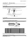
1
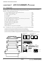
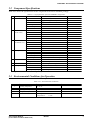
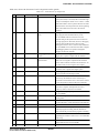
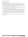
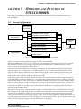
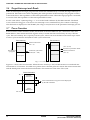
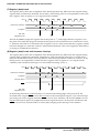
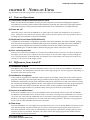
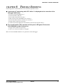
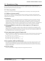
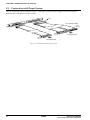
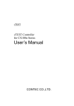
MF873-03
CMOS 4-BIT SINGLE CHIP MICROCOMPUTER
S5U1C63000H1 Manual
(S1C63 Family In-Circuit Emulator)
NOTICE
No part of this material may be reproduced or duplicated in any form or by any means without the written permission of Seiko
Epson. Seiko Epson reserves the right to make changes to this material without notice. Seiko Epson does not assume any
liability of any kind arising out of any inaccuracies contained in this material or due to its application or use in any product or
circuit and, further, there is no representation that this material is applicable to products requiring high level reliability, such
as medical products. Moreover, no license to any intellectual property rights is granted by implication or otherwise, and there
is no representation or warranty that anything made in accordance with this material will be free from any patent or copyright
infringement of a third party. This material or portions thereof may contain technology or the subject relating to strategic
products under the control of the Foreign Exchange and Foreign Trade Law of Japan and may require an export license from
the Ministry of International Trade and Industry or other approval from another government agency.
MS-DOS, Windows, Windows 95, Windows 98 and Windows NT are registered trademarks of Microsoft Corporation, U.S.A.
PC-DOS, PC/AT, PS/2, VGA, EGA and IBM are registered trademarks of International Business Machines Corporation, U.S.A.
NEC PC-9800 Series and NEC are registered trademarks of NEC Corporation.
All other product names mentioned herein are trademarks and/or registered trademarks of their respective owners.
© SEIKO EPSON CORPORATION 2001 All rights reserved.
The information of the product number change
Starting April 1, 2001, the product number will be changed as listed below. To order from April 1,
2001 please use the new product number. For further information, please contact Epson sales
representative.
Configuration of product number
Devices
S1
C
63158
F
0A01
00
Packing specification
Specification
Package (D: die form; F: QFP)
Model number
Model name (C: microcomputer, digital products)
Product classification (S1: semiconductor)
Development tools
C
63000
S5U1
A1
1
00
Packing specification
Version (1: Version 1 ∗2)
Tool type (A1: Assembler Package ∗1)
Corresponding model number
(63000: common to S1C63 Family)
Tool classification (C: microcomputer use)
Product classification
(S5U1: development tool for semiconductor products)
∗1: For details about tool types, see the tables below. (In some manuals, tool types are represented by one digit.)
∗2: Actual versions are not written in the manuals.
Comparison table between new and previous number
S1C63 Family processors
S1C63 Family peripheral products
Previous No.
New No.
Previous No.
New No.
E0C63158
E0C63256
E0C63358
E0C63P366
E0C63404
E0C63406
E0C63408
E0C63F408
E0C63454
E0C63455
E0C63458
E0C63466
E0C63P466
S1C63158
S1C63256
S1C63358
S1C6P366
S1C63404
S1C63406
S1C63408
S1C6F408
S1C63454
S1C63455
S1C63458
S1C63466
S1C6P466
E0C63467
E0C63557
E0C63558
E0C63567
E0C63F567
E0C63658
E0C63666
E0C63F666
E0C63A08
E0C63B07
E0C63B08
E0C63B58
S1C63467
S1C63557
S1C63558
S1C63567
S1C6F567
S1C63658
S1C63666
S1C6F666
S1C63A08
S1C63B07
S1C63B08
S1C63B58
Previous No.
E0C5250
E0C5251
New No.
S1C05250
S1C05251
Comparison table between new and previous number of development tools
Development tools for the S1C63 Family
Development tools for the S1C63/88 Family
Previous No.
New No.
Previous No.
New No.
ADP63366
ADP63466
ASM63
GAM63001
ICE63
PRC63001
PRC63002
PRC63004
PRC63005
PRC63006
PRC63007
URS63366
S5U1C63366X
S5U1C63466X
S5U1C63000A
S5U1C63000G
S5U1C63000H1
S5U1C63001P
S5U1C63002P
S5U1C63004P
S5U1C63005P
S5U1C63006P
S5U1C63007P
S5U1C63366Y
ADS00002
GWH00002
URM00002
S5U1C88000X1
S5U1C88000W2
S5U1C88000W1
CONTENTS
CONTENTS
CHAPTER
1 INTRODUCTION ____________________________________________ 1
CHAPTER
2 S5U1C63000H1 PACKAGE __________________________________ 2
2.1
2.2
2.3
2.4
2.5
CHAPTER
3 CONNECTION _____________________________________________ 7
3.1
3.2
3.3
3.4
CHAPTER
General of Operation ................................................................................... 11
Break Function ............................................................................................. 12
Monitoring Terminals .................................................................................. 12
Display During Execution and During Break ............................................. 13
Break Commands ......................................................................................... 13
Target Interrupt and Break .......................................................................... 14
Trace Function ............................................................................................. 14
Trace Mode .................................................................................................. 15
Trace Trigger Point ...................................................................................... 15
Coverage Function ...................................................................................... 15
Measurement of Execution Time .................................................................. 15
Self Diagnosis Function ............................................................................... 16
Restrictions on Emulation ........................................................................... 16
6 NOTES ON USING __________________________________________ 19
6.1
6.2
CHAPTER
Operation in ICE Mode ................................................................................ 9
Operation in Free Run Mode ........................................................................ 9
5 OPERATION AND FUNCTION OF S5U1C63000H1 __________________ 11
5.1
5.2
5.3
5.4
5.5
5.6
5.7
5.8
5.9
5.10
5.11
5.12
5.13
CHAPTER
AC Cable ....................................................................................................... 7
DC Cable ...................................................................................................... 7
Connection with Host Personal Computer ................................................... 7
Installing Peripheral Circuit Board (S5U1C63xxxP) .................................. 8
4 GETTING STARTED _________________________________________ 9
4.1
4.2
CHAPTER
Components .................................................................................................. 2
Component Specifications ............................................................................ 3
Environmental Conditions for Operation ..................................................... 3
Specifications of Operation Panels .............................................................. 4
Setting the Dip Switch ................................................................................... 6
Notes on Operations .................................................................................... 19
Differences from Actual IC .......................................................................... 19
7 MAINTENANCE AND WARRANTY ________________________________ 20
7.1
7.2
Diagnosis Test .............................................................................................. 20
Warranty ....................................................................................................... 20
S5U1C63000H1 MANUAL
(S1C63 FAMILY IN-CIRCUIT EMULATOR)
EPSON
i
CONTENTS
CHAPTER
8 TROUBLE SHOOTING ________________________________________ 21
CHAPTER
9 SPECIFICATIONS OF LCD63001 _______________________________ 22
9.1
Introduction .................................................................................................. 22
9.1.1 General description of LCD63001 ........................................................... 22
9.1.2 External view of LCD63001 ...................................................................... 22
9.2
Precautions on Using ................................................................................... 23
9.2.1 Notes on operations .................................................................................. 23
9.2.2 Difference from an actual IC .................................................................... 23
9.3
9.4
ii
Connection with Target System .................................................................... 24
Product Specifications ................................................................................. 26
EPSON
S5U1C63000H1 MANUAL
(S1C63 FAMILY IN-CIRCUIT EMULATOR)
CHAPTER 1: INTRODUCTION
CHAPTER 1
INTRODUCTION
S5U1C63000H1 (In-Circuit Emulator for S1C63 Family) is a hardware tool to effectively develop software
for the S1C63 Family, 4-bit single chip microcomputers. In combination with the Peripheral Circuit Board
(S5U1C63xxxP), it provides the development environment of the software using a personal computer as a
host computer, which requires Windows Ver. 3.1 or later.
This manual describes the operation of the S5U1C63000H1 hardware and connections of the
S5U1C63000H1 system. Refer to "S5U1C63000A Manual" for use of the debugging commands.
Figure 1.1 shows the external view of the S5U1C63000H1.
∗ The name 'ICE63' on the development
tool is the old name of the product.
Fig. 1.1 External view of S5U1C63000H1
S5U1C63000H1 MANUAL
(S1C63 FAMILY IN-CIRCUIT EMULATOR)
EPSON
1
CHAPTER 2: S5U1C63000H1 PACKAGE
CHAPTER 2
S5U1C63000H1 PACKAGE
2.1 Components
This package is in common with all models of the S1C63 Family. After unpacking the S5U1C63000H1
package, check to see that all of the following components are included.
Figure 2.1.1 shows the packing structure.
(1) S5U1C63000H1 (main unit with LCD63001 board) .................................. 1 unit
(2) RS232C cable (for IBM PC/AT) .................................................................... 1 cable
(3) RS232C cable (for PC-9801) ........................................................................... 1 cable
(4) AC adapter ....................................................................................................... 1 pcs.
(5) AC cable ........................................................................................................... 1 cable
(6) Jig for installing/dismounting board ......................................................... 2 pcs.
(7) S5U1C63000H1 (S1C63 Family In-Circuit Emulator) (this manual) ...... 1 copy
(8) Flat cable with 50-pin × 2 connectors .......................................................... 1 pair
(9) Flat cable with 34-pin connector .................................................................. 1 cable
(10) 50-pin connector for target system .............................................................. 2 pcs.
(11) 34-pin connector for target system .............................................................. 1 pcs.
(12) User registration card .................................................................................... 1 card
(13) Warranty card .................................................................................................. 1 card
(14) Precautions on using the S5U1C63000H1 .................................................. 1 sheet
Note: Following items need to be provided separately, not included in this package.
(15) S5U1C63xxxP board (included in the S5U1C63xxxP package)
(16) S5U1C63xxxP Manual (included in the S5U1C63xxxP package)
(17) S1C63 Family Debugger (included in the S1C63 Family Assembler package)
(18) S1C63 Family Assembler Package Manual (included in the S1C63 Family Assembler package)
•S5U1C63000H1
Manual
EPSON
EPSON
CMOS 4-bit Microcomputer S1C63 Family
Registration
..............
..........
............
........
CMOS 4-bit Microcomputer S1C63 Family
S5U1C63000H1 Manual
S5U1C63000H1 Manual
SEIKO EPSON CORPORATION
English
•User registration card
•Warranty card
•Precautions on using the ICE63
Registration
..............
..........
............
........
SEIKO EPSON CORPORATION
Japanese
English
Japanese
•S5U1C63000H1 main unit
G
O
U
T
TR
C
BR IN
K
IN
G
N
D
TR
PO
W
ER
SLPEM
U
/H
LT
PC
15
PC
14
PC
13
PC
12
PC
11
PC
10
PC
9
PC
8
PC
7
PC
6
PC
5
PC
4
PC
3
PC
2
PC
1
PC
0
12345678
UT
OPO
ST
ICE
RS232C
RUN
ICE63
SEIKO EPSON CORP.
•AC adapter
•Connectors
for target system
•Jigs
•AC cable
(50-pin × 2) (34-pin × 1)
(× 2)
•Flat cables
•RS232C cables
(for IBM PC/AT)
(50-pin × 2)
(for PC-98 Series)
(34-pin × 1)
Fig. 2.1.1 Packing structure
2
EPSON
S5U1C63000H1 MANUAL
(S1C63 FAMILY IN-CIRCUIT EMULATOR)
CHAPTER 2: S5U1C63000H1 PACKAGE
2.2 Component Specifications
Table 2.2.1 shows the specifications of the component in the S5U1C63000H1 package.
Table 2.2.1 Specifications of S5U1C63000H1 components
No.
1
2
3
4
Components
Items
Specifications
Dimensions
Weight
282 (W) × 177 (L) × 90 (H)
Approx. 3.5 kg (main body)
External color
Cygnus white
Input voltage
DC 5 V
Power consumption
Board mounted
2 A, max.
ICE board and LCD board
RS232C cable
Length
3m
(for PC-9801)
Interface level
Cable
EIA-RS232C level
12-pair shielded cab tyre cable
Cable-ended connector
DBC-25P-F0
Connector on host
Length
Interface level
DBC-25S
3m
EIA-RS232C level
Cable
Cable-ended connector
Connector on host
12-pair shielded cab tyre cable
DBC-25P-F0, DEU 9S-F0
DE-9P
Dimensions
160 × 80 × 60
Input voltage
Input frequency
Power consumption
AC 90 V to 264 V
47 Hz to 63 Hz
25 W, max. (in ICE system load)
S5U1C63000H1
RS232C cable
(for IBM PC/AT)
AC adapter
Remarks
Rubber feet included
∗
or equivalent
or equivalent
5
AC cable
Output voltage•current
Length
DC 5 V/5 A, with over current protection
1.8 m
6
7
Accessories
Package
Plug type
Jig
Dimensions
Bipolar with ground
for installing/dismounting PRC/LCD board
380 (W) × 260 (L) × 225 (H)
Materials
Total weight of package
W carton, cardboard
Approx. 5 kg
Outside: 5 V, Inside: 0 V
∗ Peripheral Circuit Board is sold separately
2.3 Environmental Conditions for Operation
Table 2.3.1 shows the environmental conditions to operate S5U1C63000H1 that has to be used.
Table 2.3.1 Environmental conditions
No.
1
2
Items
Operating temperature
Storage temperature
5 to 40 °C
-10 to 60 °C
Specifications
3
4
5
Operating humidity
Storage humidity
Resistance to vibration
35 to 80%
20 to 90%
Operating:
No condensation
0.25 m/S2
Transportation:
S5U1C63000H1 MANUAL
(S1C63 FAMILY IN-CIRCUIT EMULATOR)
Remarks
1 m/S2
EPSON
3
CHAPTER 2: S5U1C63000H1 PACKAGE
2.4 Specifications of Operation Panels
This section explains the operation of each switch. Figure 2.4.1 shows the external view of the panels.
T
OU
OP
ST
O
U
T
TR
C
BR IN
K
IN
G
N
D
TR
G
PO
W
ER
SL EM
P/ U
H
L
PC T
1
PC 5
1
PC 4
1
PC 3
1
PC 2
1
PC 1
10
PC
9
PC
8
PC
7
PC
6
PC
5
PC
4
PC
3
PC
2
PC
1
PC
0
12345678
ICE
RS232C
RUN
ICE63
SEIKO EPSON CORP.
(Front view)
OFF
ON
POWER
DC 5V
(Rear view)
(Front)
(Rear)
CB
(Side view)
Fig. 2.4.1 External view of S5U1C63000H1 panels
4
EPSON
S5U1C63000H1 MANUAL
(S1C63 FAMILY IN-CIRCUIT EMULATOR)
CHAPTER 2: S5U1C63000H1 PACKAGE
Table 2.4.1 shows the function of each component on the panels.
Table 2.4.1 Function list of components
No.
1
Position
Side panel
Indicated symbol
CB
Name
Function
Circuit breaker
The breaker cuts off the power of S5U1C63000H1
system (ICE board, LCD board, PRC board and target
board) at consumption current of 4 A or more. A small
staff of the breaker comes up at the shut-off. The staff
should be at the recessed position for normal operating
status. The breaker does not work at the normal
operation.
2
Front panel
ICE/RUN
ICE mode/Free run mode
switch
Shifting the switch to "RUN" (slant to right) loads a
target program from the flash memory in the
S5U1C63000H1 without connection to a host
computer and gets the system into free run status of
the target program. In this mode, however, debugging
function such as brake and trace does not work.
Shifting the switch to "ICE " (slant to left) enables the
S5U1C63000H1 to be connected with a host computer
and debugging function is operative through the
3
Front panel
TRGOUT
Tracing trigger output
terminal
debugger on the host computer.
Upon coincidence of trigger conditions with a tracing
trigger point, a pulse is output from this terminal.
4
Front panel
STOPOUT
HALT/SLEEP status
output terminal
When the S1C63000 CPU is in HALT or SLEEP
status, low level signal is output from this terminal.
5
Front panel
TRCIN
Trace input terminal
This is used to measure execution rate of the CPU. At
the break mode, low level signal is also output.
Information is stored in the trace memory by
6
Front panel
BRKIN
Break input terminal
connection with a signal of the target system.
A running program enters in break status by input a
7
Front panel
GND
Ground terminal for above
8
Front panel
DSW1–8
low level signal from the target system.
In case the above terminal is monitored with such an
oscilloscope, the GND line of the oscilloscope is
connected to this terminal. This is also used as a GND
in case the signals are input to the above terminals.
This is a switch to set a baud rate of communication
DIP switch
with a host computer. 9600 bps has been set at
ex-factory. Refer to Section 2.5 for details.
9
Front panel
POWER
Power-on LED
10 Front panel
EMU
Emulation LED
11 Front panel
SLP/HLT
Halt LED
12 Front panel
PC15–0
Program counter indicator
13 Front panel
RS232C
RS232C connector
14 Rear panel
DC 5V
DC input connector
15 Rear panel
POWER
Power switch
S5U1C63000H1 MANUAL
(S1C63 FAMILY IN-CIRCUIT EMULATOR)
EPSON
This green LED lights upon power-on of
S5U1C63000H1.
This red LED lights when the target program is in
running status.
This yellow LED lights when the S1C63000 CPU
executes the HALT or SLP instruction. This LED also
lights when the PRC board has not been installed.
These LEDs indicate the program counter (PC) value
while the program is running and also hold the PC
value at the break point while the program is breaking.
This is a connector to connect a RS232C cable.
Tightening the connector with screws is recommended
while using.
This is a connector to connect the DC cable of the AC
adapter dedicated for S5U1C63000H1.
Turns the S5U1C63000H1 power on and off.
5
CHAPTER 2: S5U1C63000H1 PACKAGE
2.5 Setting the Dip Switch
The S5U1C63000H1 works with a personal computer that runs MS-Windows Ver. 3.1 or later as a host.
With a general computer that meets the condition, the serial transfer rate set at the factory (9600 bps) is
good for use. In case the rate is changed, the transfer rate between the host computer can be changed by
this switch. The switch also sets a self diagnostic function, which is equipped in the S5U1C63000H1,
working or not working at the power on. Figure 2.5.1 shows the dip switch.
—OPEN—
1
2
3
4
5
6
7
8
Fig. 2.5.1 Dip switch
<Setting baud rate>
SW1–3
SW4
OPEN
OPEN
OPEN
OPEN
OPEN
ON
OPEN
OPEN
OPEN
ON
Other settings
SW5
OPEN
ON
OPEN
OPEN
ON
SW6
OPEN
ON
ON
ON
OPEN
Baud rate setting
9600 bps, 8-bit character, 1 stop bit, no parity (factory setting)
2400 bps, 8-bit character, 1 stop bit, no parity
4800 bps, 8-bit character, 1 stop bit, no parity
19200 bps, 8-bit character, 1 stop bit, no parity
38400 bps, 8-bit character, 1 stop bit, no parity
Do not set.
Note: The setting at the host end is recommended to be "9600 bps, 8-bit character, 1 stop bit, no parity".
<Setting the self diagnostic function>
SW8
OPEN
ON
Setting
Self diagnosis On
Self diagnosis Off (factory setting)
Note: When the S5U1C63000H1 is started with the self diagnosis on, it takes approx. 5 minuets to be
ready for use.
Open means that the switch lever is at upper side.
On means that it is at lower side.
6
EPSON
S5U1C63000H1 MANUAL
(S1C63 FAMILY IN-CIRCUIT EMULATOR)
CHAPTER 3: CONNECTION
CHAPTER 3
CONNECTION
This chapter describes the connection between the S5U1C63000H1 and a host computer and the Peripheral Circuit Board (S5U1C63xxxP).
3.1 AC Cable
The S5U1C63000H1 package includes a dedicated AC cable (3 poles type) and an AC adapter. The AC
cable is connected into the AC inlet on the AC adapter. The common ground frame line should be used
for connecting the S5U1C63000H1 and the host computer as shown in Figure 3.1.1.
Host machine
S5U1C63000H1
DCIN (DC 5 V)
terminal
AC adapter dedicated for S5U1C63000H1
AC inlet
DC cable
AC cable
AC line
Frame ground line
Fig. 3.1.1 Connection of AC line
3.2 DC Cable
The DC output cable of the AC adapter is connected to the DCIN (DC 5 V input) terminal as shown in
Figure 3.1.1.
3.3 Connection with Host Personal Computer
Figure 3.3.1 shows the external view of the RS232C cable connector and Table 3.3.1 shows the signal
specifications of the RS232C cable.
1 2 3
13
A
14
25
Viewed from side A
25-pin RS232C cable connector
Fig. 3.3.1 External view of the RS232C cable connector
Table 3.3.1 Signal specifications
Terminal No. Signal name
Signal meaning
2
TXD
Transmit data from HOST to ICE
3
4
5
RXD
RTS
CTS
Receive data from ICE to HOST
Request to send from HOST
Clear to send from ICE
1
7
FG
SG
Frame ground
Signal ground
Remarks
Normally used as ON
Normally used as ON
To connect with NEC PC-9801 series and their compatibles, use the 25-pin/25-pin cable. The RS232C
cable has the same connector at both end so that there is no directional restriction on its usage. To connect
with IBM PC/AT and its compatibles, use the 9-pin/25-pin cable. Tightening the connectors with the
screws is strongly recommended after the connection.
S5U1C63000H1 MANUAL
(S1C63 FAMILY IN-CIRCUIT EMULATOR)
EPSON
7
CHAPTER 3: CONNECTION
3.4 Installing Peripheral Circuit Board (S5U1C63xxxP)
By installing a Peripheral Circuir Board (to be separately sold) into a slot of the S5U1C63000H1, a debug
system can be made corresponding to each device of the S1C63 Family. Figure 3.4.1 shows installing
method of the Peripheral Circuir Board. The S5U1C63000H1 is equipped with a main control board and a
LCD drive board.
(1), (4)
(2)
Peripheral Circuit Board
(2), (3)
Fig. 3.4.1 Installing method of the Peripheral Circuit Board
(1) Unfasten the screws located on the left and right sides of the front panel of the S5U1C63000H1 by
turning them counterclockwise, then remove the front panel.
(2) Insert the Peripheral Circuir Board into
the uppermost slot and push it using the
jig attached with the S5U1C63000H1 as
shown in Figure 3.4.2.
Peripheral Circuit Board
Using this jig as a lever, push it toward
the inside of the board evenly on the left
and right sides. After confirming that the
Peripheral Circuir Board has been firmly
fitted into the internal slot of the
S5U1C63000H1, remove the jig.
Fig. 3.4.2 Installing the Peripheral Circuit Board
(3) Dismounting Peripheral Circuir Board
Set the jig into position as shown in
Figure 3.4.3. Using this jig as a lever,
push it toward the outside of the board
evenly on the left and right sides and
pull the Peripheral Circuir Board out of
the S5U1C63000H1.
Peripheral Circuit Board
(4) Mounting the front panel
Mount the front panel removed at the
step (1) on the main case by pushing and
turning two screws located at both side.
Fig. 3.4.3 Dismounting the Peripheral Circuit Board
(5) The jig has a magnet for keeping under the bottom plate of the case while not in use.
8
EPSON
S5U1C63000H1 MANUAL
(S1C63 FAMILY IN-CIRCUIT EMULATOR)
CHAPTER 4: GETTING STARTED
CHAPTER 4
GETTING STARTED
There are two operation modes in the S5U1C63000H1. One is ICE mode to be started with the debugger
in connection with a host machine (the ICE/RUN switch on the front panel is set to ICE side) and the
other one is free run mode to run a target program without a host machine (the ICE/RUN switch is set to
RUN side).
4.1 Operation in ICE Mode
After the S5U1C63000H1 and the host machine is connected with the RS232C cable and the ICE/RUN
switch is set to ICE side, turn the host machine and S5U1C63000H1 power on. It enables the
S5U1C63000H1 to be controllable by the host machine and the debugger "db63.exe" can be executed on
the host. Following shows the operation sequence of the S5U1C63000H1 after power-on.
(1) Turning the S5U1C63000H1 power on
The power LED (green) is on, and the SLP/HLT LED (yellow) is momentary on. The PC8 and PC4
LEDs (red) go on (program counter is 110H).
(2) Starting the debugger
Upon starting the debugger (db63.exe) on the host, the SLP/HLT LED (yellow) goes momentary on.
(3) Execution of a target program
When the debugger starts execution of a target program, the EMU LED (red) is turned on to indicate
the emulation mode. While the target program is executed, the PC LEDs (red) indicate the current
program counter value. When the SLP or HLT instruction is executed, the SLP/HLT LED (yellow)
goes on and the PC LEDs (red) stop.
(4) Occurrence of a break
When the target program stops at the break point set with the debugger, the EMU LED (red) goes off
and the PC LEDs (red) stops at the break address. The break address means the program counter of
next execution.
4.2 Operation in Free Run Mode
By turning the S5U1C63000H1 power on after the ICE/RUN switch located on the front panel is set to
RUN side, the S5U1C63000H1 enters in the free run mode that executes the target program continuously.
Following shows the execution flow of the target program in the free run mode.
(1) Turning the S5U1C63000H1 power on
The power LED (green) is on, and the SLP/HLT LED (yellow) is momentary on. PC8 and PC4 LEDs
(red) go on (program counter is 110H).
(2) Setting data from flash memory
The S5U1C63000H1 read the configuration information and various mask option information for each
model from the built-in flash memory and set them to the controller. The target program is also read
from the flash memory and transferred to the built-in emulation memory.
(3) Execution of the target program
The S5U1C63000H1 executes the target program from the reset address. The PC LEDs (red) indicate
the current program counter position during execution. When the SLP or HALT instruction is executed, the SLP/HLT LED (yellow) goes on and the PC LEDs (red) stop.
S5U1C63000H1 MANUAL
(S1C63 FAMILY IN-CIRCUIT EMULATOR)
EPSON
9
CHAPTER 4: GETTING STARTED
● Notes on free run mode
(1) Any configuration information, various mask information and target program have not been written
in the flash memory built into the S5U1C63000H1 at the time of ex-factory. Even though the
S5U1C63000H1 enters in the free run mode without the data, it does not execute any target program
and while the program counter on the front panel indicates the reset address of 110H. Therefore, it is
necessary to write a target program, configuration information and various mask option information
into the flash memory in the ICE mode before setting the free run mode.
(2) In the free run mode, the break functions and the trace functions can not be used. The free run mode
only execute a target program and display the current program counter with the LEDs on the front
panel. The BRKIN terminal on the front panel becomes invalid.
(3) In the case any incorrect access exceeding configured program size or data RAM size is occurred by
reason of a improper target program, the S5U1C63000H1 immediately stops at the program counter,
where the incorrect access is made, by the LEDs on the front panel. In order to reset this situation, the
power should be off. Before the free run of the target program is carried out again, the program must
be completely debugged on the ICE mode. In the case any control to exceed program sizes such as
jump or call to outside of the program, it stops before the access to an incorrect area. In the case any
control to exceed data size such as read or write into outside of the data RAM area, it stops after the
access to the incorrect area.
(4) The S5U1C63000H1 may takes approx. 5 minuets after it is turned on until it starts execution of the
target program.
10
EPSON
S5U1C63000H1 MANUAL
(S1C63 FAMILY IN-CIRCUIT EMULATOR)
CHAPTER 5: OPERATION AND FUNCTION OF S5U1C63000H1
CHAPTER 5
OPERATION AND FUNCTION OF
S5U1C63000H1
This chapter describes operations, functions in detail and restrictions in the emulation mode of the
S5U1C63000H1.
5.1 General of Operation
ICEcontrol
processor
Emulation control portion
Emulation program memory
RS-232C
host interface
Emulation data memory
S1C63000
CPU
Trace control portion
Break control portion
Target monitor portion
To PRC board
ICE firmware
Flash memory
Fig. 5.1.1 Functional block diagram of S5U1C63000H1
Figure 5.1.1 shows the functional block diagram of the S5U1C63000H1.
The S5U1C63000H1 has a processor to control in-circuit emulation, which processes the ICE commands.
The function to execute or stop target programs by the S1C63000 CPU is called emulation, of which
control is done by the emulation control section.
Operation that the S1C63000 CPU is working (specified by the G command) and single step operation
(specified by the S or N commands) are called emulation mode, on which the EMU LED goes on and
program counter display LEDs real timely indicate the program counter of the program running. The
other status is called standby mode, which turns the EMU LED off and makes the program counter
display LEDs show program counter position at the break.
The target program to be executed with the S1C63000 CPU is stored in the emulation program memory
and data RAM area of the S1C63000 CPU is assigned to the emulation data memory. Loading a program
from the flash memory or the host is done by the S5U1C63000H1 control processor in the standby mode.
The trace control portion records execution bus cycle of the S1C63000 CPU and consists of a memory of
8,192 words × 120 bits. Such large size memory enables the register value inside the S1C63000 CPU to be
real timely recorded. The tracing is done in the emulation mode and it is analyzed by the ICE control
processor in the standby mode.
The break control portion compares the bus condition of the S1C63000 CPU with break points and stops
the execution of the target program upon coincident. The break can be also real timely made by register
values of the S1C63000 CPU. While a target program is running, the target monitor portion of the ICE
control processor monitors executing program counter value of the S1C63000 CPU and RAM contents at
watching points. The monitored result is displayed as on-the-fly information. The S1C63000 CPU can real
timely execute the target program while the information is displayed.
S5U1C63000H1 MANUAL
(S1C63 FAMILY IN-CIRCUIT EMULATOR)
EPSON
11
CHAPTER 5: OPERATION AND FUNCTION OF S5U1C63000H1
5.2 Break Function
● Forced break
The debugger on the host machine can forced break the emulation. This function is useful when the
program counter does not proceed by executing the SLP or HALT instruction in a single step process.
● Break commands
Some break commands are available to set various breaking conditions. A break occurs when the
break condition specified by the command and status of the S1C63000 CPU are met.
● Break by accessing to undefined area
This break occurs when the target program accesses an address exceeding the ROM capacity of the
actual chip. The break is also occurred when any address other than the RAM area or mapped I/O
area of the actual chip is accessed.
● Break by accessing write protect area
This break occurs when the target program writes data to the read only memory such as a character
generator ROM. The memory contents are protected even this break occurs.
● Break by incorrect stack accessing
This break occurs when the target program makes incorrectly stacking operation exceeding the
defined stack area in the S1C63000 CPU.
● BRKIN terminal
When a signal is input to the BRKIN terminal, a break occurs at the falling edge of the signal.
5.3 Monitoring Terminals
● TRGOUT output terminal
A low level pulse is output at the T3 state of the clock when the trace trigger condition and the bus
cycle are met.
T1
CLK from
Peripheral Circuit board
T2
T3
T4
PK
PL
Bus cycle
Coincidence with trace trigger
TRGOUT output
Fig. 5.3.1 TRGOUT terminal output
● STOPOUT output terminal
A low level is output when the S1C63000 CPU is suspended (by execution of the HALT or SLP
instructions). This terminal also outputs low level during break.
STOPOUT output
Indicating suspension
of CPU operation
Running
Breaking
Fig. 5.3.2 STOPOUT terminal output
12
EPSON
S5U1C63000H1 MANUAL
(S1C63 FAMILY IN-CIRCUIT EMULATOR)
CHAPTER 5: OPERATION AND FUNCTION OF S5U1C63000H1
● TRCIN input terminal
By connecting a signal line of the target system to this terminal, trace information is stored into the
trace memory. "1" is written to the trace memory when it is not connected or the signal is at high level,
and "0" is written to the trace memory when the signal is at low level. The signal is sampled at the
rising edge of T4 state.
● BRKIN input terminal
A break occurs when a low level signal is input to this terminal while the target program is running.
To use this terminal for the break function , the low level pulse must be 20 msec or longer. By connecting the TRGOUT output terminal to the BRKIN input terminal, breaks can be occur according to the
trace trigger conditions.
5.4 Display During Execution and During Break
The ICE control processor monitors the execution status of the S1C63000 CPU while the target program is
running. It displays the S1C63000 CPU’s execution status in every 500 msec when the on-the-fly display
mode is specified. Program counter value that are displayed during break show the address to be executed in next step. Values in all registers are at the time of the break.
The LED’s (PC15–PC0) on the front panel indicate the executed program counter value during execution,
and stops at the break address when a break occurs.
5.5 Break Commands
The S5U1C63000H1 has abundant break functions.
(1) PC break
This break function is specified by the BP command. When the program counter of the S1C63000 CPU
coincides with the specified address, a break occurs before executing the instruction. Multiple PC
values (up to maximum size of program memory) can be specified as break points.
(2) PC sequential break
This break function is specified by the BS command. The break occurs when the PC of the S1C63000
CPU counts three addresses in specified order. The pass count can be specified for the last address.
The sequence (address 1 coincidence) → (address 2 coincidence) → (address 3 counted by specified
times) breaks the execution.
(3) Break by data access
This break function is specified by the BD command. The break occurs immediately after the target
program accesses the data memory in the specified condition (AND condition of address, data and
read/write operation). It is possible to specify a range for the address condition, a mask in bit units
for the data condition and a mask for the read/write condition. This specification can set one break
point only.
(4) Break by register value
This break function is specified by the BR command. When the register values of the S1C63000 CPU
coincides with the specified values, a break occurs immediately after the instruction is executed.
An AND condition of A/B registers, E/I/C/Z flags and X/Y registers can be specified. It is also
possible to specify masking on each register. This specification can set one break point only.
The above break functions, (1), (2), (3), (4), can be independently specified. When the target program is
executed with all specified commands, BP, BS, BD, BR, breaks occur by meeting any condition.
S5U1C63000H1 MANUAL
(S1C63 FAMILY IN-CIRCUIT EMULATOR)
EPSON
13
CHAPTER 5: OPERATION AND FUNCTION OF S5U1C63000H1
5.6 Target Interrupt and Break
When an interrupt in the target program and a break are simultaneously occurred, the target interrupt is
prioritized. The break occurs after completing the stack operation of the interrupt. The program counter
at the break shows the top address of the interrupt handler routine. When the target program is restarted,
it executes from the top address of the interrupt handler routine.
It is the same when "I (interrupt flag) = 1" is set as the break condition by the BR command. The break
occurs when the I flag goes 1. However if an interrupt occurs simultaneously, the contents of the flags
after the break is displayed as "EICZ:0000" (the I flag is reset) because of the prioritized interrupt process.
5.7 Trace Function
In the execution of the emulation mode, information of the S1C63000 CPU (PC, instruction code, data
RAM address, data content and CPU register value) is stored into the trace memory at every CPU bus
cycle. The trace memory has a capacity of 8,192 cycles, which can store the latest instructions up to 4,096
in 2 bus cycles instruction and 2,048 in 4 bus cycles instruction.
Trace memory
Trace memory
Earliest instruction
(TP = 0)
Effective trace
Effective trace
Execution of
a program
Instruction just before
break (TP = 700)
(TP = 8,191)
Instruction just before break
Earliest instruction
(TP = 0)
Effective trace
Free space
Fig. 5.7.1 Trace function
Figure 5.7.1 shows the trace function. When the trace memory is full, old information is erased and new
information is overwritten. TP called trace pointer shows that the point of 0 means the earliest instruction
and the break point means the latest information. The maximum value of the TP is 8,191.
Trace information
TP = 0
Earliest
instruction
Trace information at any point can be displayed
by the TD command.
Latest
instruction
TP = 8,191
14
EPSON
S5U1C63000H1 MANUAL
(S1C63 FAMILY IN-CIRCUIT EMULATOR)
CHAPTER 5: OPERATION AND FUNCTION OF S5U1C63000H1
5.8 Trace Mode
There are following three trace modes.
(1) All bus cycle trace mode
In this trace mode, all bus cycles are traced during run emulation and step emulation until a break
occurs.
(2) Specified PC range trace mode
In this mode, bus cycles within the specified range (or outside the specified range) are traced during
run emulation and step emulation until a break occurs. This function is useful for cases of tracing
objective work data only or removing WAIT routine from the trace.
(3) Single delay trigger
In this mode, starting a run emulation starts tracing all bus cycles. When the emulation hit the trace
trigger condition, the trace continues for the specified bus cycles, and then it stops. The trace information is displayed after a break.
In the db63 debugger, one of the above modes can be selected by the TM command.
5.9 Trace Trigger Point
In the S5U1C63000H1, a trace trigger point can be specified independent of breaking points. The trace
trigger point is specified as the program counter conditions of the S1C63000 CPU. A low level pulse is
output from the TRGOUT terminal with the timing of T3 upon coincidence of the specified value and the
program counter. The information of the trace trigger point is also stored into the trace memory. In the
single delay trigger mode, the trace trigger point becomes a condition for stopping the trace.
5.10 Coverage Function
The S5U1C63000H1 can retrieve and display the address information of the program accessed at the
execution. The confirmation of portions whether failure analysis or debugging is completed or not can be
done by checking the program through reference of the coverage information after running the program
for a long time. This function is specified by the CV or CVC commands.
5.11 Measurement of Execution Time
The S5U1C63000H1 has a function to measure the time from start to break of target programs or to count
the bus cycles. This function is set by the MD command.
(1) Time measurement mode
(a) Range of time measurement
1 µsec to 1∗(231 -1) µsec (≈ 2,147 sec ≈ 36 minutes)
(b) Measurement error
±1 µsec
(c) Units of time display
Micro second (µsec)
(2) Bus cycle count mode
(a) Range of cycle measurement
1 bus cycle to (231 -1) bus cycles (= 2∗109 bus cycles)
(b) Measurement error
0 cycle
S5U1C63000H1 MANUAL
(S1C63 FAMILY IN-CIRCUIT EMULATOR)
EPSON
15
CHAPTER 5: OPERATION AND FUNCTION OF S5U1C63000H1
5.12 Self Diagnosis Function
In the S5U1C63000H1, it is possible to select whether the self diagnosis at power on is executed or not.
(1) No self diagnosis mode (DSW8: on, factory setting)
When the DIP switch 8 on the front panel of the S5U1C63000H1 is set to on, the S5U1C63000H1
becomes ready to accept commands without the self diagnosis after power on.
(2) Self diagnosis mode (DSW8: open)
When the switch is set to open, the S5U1C63000H1 execute following self diagnosis after power on,
and then it becomes ready to accept commands.
(a) ROM test
Check-sum test of the firmware
(b) RAM test
Read/write test of the RAM in the S5U1C63000H1
(c) Flash memory test
Check sum test of the flash memory
(d) Emulation test
Tests the break function by executing a run emulation for a few steps on the emulation memory.
The self diagnosis takes about five minutes after power on.
If an error is displayed while testing, it is considered to be failure of the hardware. Please consult us.
5.13 Restrictions on Emulation
(1) Timer operation in standby mode
In the emulation with Peripheral Circuir Board connected to the S5U1C63000H1, the S1C63000 CPU is
ordinarily at the idle status (standby mode) as shown in Section 5.1. In the standby mode, the
S5U1C63000H1 executes the monitor program and the Peripheral Circuir Board is in stop status. The
S5U1C63000H1 executes the target program by the G command and returns to the monitor program
after a break occurs.
S1C63000
CPU operation
Execution of monitor program
(standby mode)
Execution of emulation
(running target program)
Execution of monitor program
(standby mode)
Fig. 5.13.1 Operation of S1C63000 CPU
In the models having a timer and a watch dog timer, the timer is operated only when the target
program is executed if the timer is active. Therefore, in the single step operation, a real time counting
cannot be done with the timers in the S1C63xxx.
16
EPSON
S5U1C63000H1 MANUAL
(S1C63 FAMILY IN-CIRCUIT EMULATOR)
CHAPTER 5: OPERATION AND FUNCTION OF S5U1C63000H1
(2) Interrupt in standby mode
In the standby mode, interrupt requests from the target system is reserved. The interrupt while the
monitor program is being executed is accepted at the execution of the target program. For instance,
when an interrupt request from the target system is generated while breaking, the interrupt is accepted immediately after the target program restarts if the interrupt is enabled in the S1C63000 CPU.
(3) Interrupt at single step operation
Interrupts during single step operation can be enabled or disabled using the MD command. Each
operation is as follows.
• When interrupt is enabled
If an interruption request is generated while a target program step is executed by the S or N commands, the interrupt processing is done at the time of the instruction execution, and the execution
stops after fetching the vector address of the interrupt. Therefore, next single step operation executes
the interrupt handler routine. When the HALT or SLP instructions are executed by the S or N commands, the commands are executed until a interrupt is occurred. In this status, a forced break input
from the host computer suspends the execution.
• When interrupt is disabled
Interrupt processing are not executed by the S command. Therefore, the execution of the HALT or SLP
instructions is immediately suspended, and the program counter indicates an address next to the
HALT or SLP instructions. The N command operates similar to the S command in the execution of the
main routine, however, it enables interrupts regardless of the setting by the MD command in the
execution of the sub-routine.
(4) Data read from undefined RAM area
When a data RAM (ROM) area or an I/O area that is not available in the actual IC chip is read, the
read data becomes indefinite. Read data from the actual IC is also indefinite, however it is different
from the S5U1C63000H1.
(5) Detection of SP1 incorrect stack access
It is possible to detect any incorrect stack access to out of SP1 area by specifying the SP1 area with the
BSP command.
The S1C63000 CPU has a queue register and takes stack value in advance in order to make high speed
process of the stacking operation for the CALR instruction and interrupts. Therefore, when a value is
returned from the top address of the stack, it takes the stack value beyond the top address and write it
into the queue register. This operation works without any problem, however, the queue register has
an indefinite value. In order not to make this process incorrect access, it is necessary to add three
addresses onto the real using SP1 area.
(6) Data read break
In the execution of "INT addr6" instruction, setting break on the data read condition may break
program running, because dummy read cycle of a memory specified by addr6 operand is added. For
instance, when the break at read cycle is set by the break data set command (BD), the dummy read
hits the break condition.
S5U1C63000H1 MANUAL
(S1C63 FAMILY IN-CIRCUIT EMULATOR)
EPSON
17
CHAPTER 5: OPERATION AND FUNCTION OF S5U1C63000H1
(7) Register (data) break
The register (data) value after completion of the break operation may differ from the original setting
register (data) condition for the break. For instance, in the timing chart to set sequentially 5 and 6 into
the A register, if the A register is 5 as a register break condition;
CLK
Instruction execution
ld %a, 5
ld %a, 6
A register
ICE data
judgment point
➀
ICE monitor command ICE monitor command
5
6
➁
➂
The S5U1C63000H1 judges the register data at the point of "↑", and judges that the A register is 5 at
the point of ➁. When the program is broken at this point, it has executed the next command of "ld %a,
6", therefore, the break is occurred after the A register is set to 6. This means that the A register content
has been changed to 6 when the content is refereed after the break. This is also applied to the break by
accessing to undefined area function.
(8) Register (data) break and hardware interrupt
The register (data) value after completion of the break operation may differ from the original setting
register (data) condition for the break. Furthermore, when a hardware interrupt is occurred in this
point, the break address shifts to the top address of the interrupt handler routine. For instance, in the
timing chart to set sequentially 5 and 6 into the A register, if the A register is 5 as a register break
condition, and a hardware interrupt is occurred while executing "ld %a, 5";
CLK
Instruction execution
ld %a, 5
ld %a, 6
A register
5
6
➁
➂
Interrupt factor
IACK
ICE data
judgment point
➀
In the timing chart above, if the interrupt is occurred (at the falling edge) at the point of ➀, the
S1C63000 CPU outputs IACK to show the execution of the interruption response cycle. The interrupt
processing can not be stopped while this IACK is at low level. Therefore, the S5U1C63000H1 can not
stop the interrupt in spite of its judgment that the A register becomes 5 at the point of ➁ because the
IACK is at low level, and the break is occurred after jumping to the interrupt vector address.
18
EPSON
S5U1C63000H1 MANUAL
(S1C63 FAMILY IN-CIRCUIT EMULATOR)
CHAPTER 6: NOTES ON USING
CHAPTER 6
NOTES ON USING
Pay attention to the following matters for proper use of the S5U1C63000H1.
6.1 Notes on Operations
(1) Connection and disconnection between units
Make sure that the S5U1C63000H1 and the personal computer are off when installing the Peripheral
Circuir Board, connecting cables and disconnecting them. Specially, the connection of the target interface
cable with the power on may make permanent destruction of IC’s inside due to its CMOS structure.
(2) Power on, off
When the power of the S5U1C63000H1 is on again after off, remain off condition for 10 seconds or
more. The power on without such interval may result in incorrect power-on-reset operation and/or
working the circuit breaker of the S5U1C63000H1.
(3) Peripheral Circuir Board (S5U1C63xxxP)
A Peripheral Circuir Board is required for operation of the S5U1C63000H1. The S5U1C63000H1 package
does not include Peripheral Circuir Board that needs to be separately provided. If the S5U1C63000H1 is
turned on without Peripheral Circuir Board installed, the "HLT/SLP" LED on the front panel of the
S5U1C63000H1 goes on and the LEDs to indicate the program counter value show 110H.
(4) Over current protection
If the power of the S5U1C63000H1 is on under the condition that VDD and VSS are short-circuited on
the target system, the power LED does not turn on due to cut off of the output current working the
over current protection in the dedicated AC adapter. The circuit breaker cuts the power at the load
current of 3 A or more on the target system.
6.2 Differences from Actual IC
(1) Initialization of RAM
Data RAM of the actual IC becomes indefinite value, however, of the S5U1C63000H1 is initialized to
0AH. Therefore, the initialization must be done in the target program, and any program depending on
the initial value must not be made.
(2) Initialization of registers
In the actual IC, registers have indefinite values at power on and keep values prior to the reset except the
program counter (PC), the interruption flag (I) and the extension flag (E). However, the S5U1C63000H1 is
initialized to 0AH (4-bit), 0AAH ( 8-bit) and 0AAAAH (16-bit) at the power on and at the software reset by
the command of the debugger. Because of this, each register must be initialized, and any program depending on the initial value must not be made. The reset switch on the Peripheral Circuir Board and the
hardware reset input from the I/O connector keep values prior to the reset as the actual IC.
(3) Access to undefined area
In the S5U1C63000H1, the access to the undefined area causes break. However, the S5U1C63000H1
has RAM for the undefined area, and the break occurs after accessing to the undefined area, so that it
can writes any value into the undefined area. If execution of the target program is restarted after the
break by accessing to undefined area, it works with non-existing memory. Therefore, any program to
read/write into the undefined area must not be made.
(4) Data dump
The S5U1C63000H1 uses a Peripheral Circuir Board clock for access to RAM, ROM, LCD and I/O area
with the data dump command. When the I/O area is read in the target program, there may have a
time delay until the correct value is obtained due to the parasitic capacitance and the pull-up/down
resisters of each I/O terminal. Therefore, the value read on the target program may differ from the
value read by the dump command.
S5U1C63000H1 MANUAL
(S1C63 FAMILY IN-CIRCUIT EMULATOR)
EPSON
19
CHAPTER 7: MAINTENANCE AND WARRANTY
CHAPTER 7
MAINTENANCE AND WARRANTY
7.1 Diagnosis Test
The self diagnosis test is executed by setting SW8 of the DIP switch to OPEN and starting the debugger
after power of the S5U1C63000H1 on.
Debugger for E0C63 Ver x.xx
Copyright(C) SEIKO EPSON CORP. 199x
Connecting with ICE .............
DIAG test, please wait 5 min. .. done ← ➀
Parameter file name
: xxxxxxxx.par
Version
: xx
Chip name : xxxxx
CPU version
: x.x
PRC board version
: x.x
LCD board version
: x.x
EXT board version
: x.x
ICE hardware version
: x.x
ICE software version
: x.x
DIAG test
: OK.
Map ............................. done
Initialize ...................... done
>
When an error is detected, the error message is output at the point of ➀ instead of "done". If an error
message is output, stop using the S5U1C63000H1 because it may have a hardware failure.
This diagnosis test takes approx. 5 minuets for completion because of its precise inspection. Even in the
free run mode, it takes approx. 5 minuets for the self diagnosis test before the target program is executed.
7.2 Warranty
Please refer to the warranty card attached to the unit for the warranty details.
20
EPSON
S5U1C63000H1 MANUAL
(S1C63 FAMILY IN-CIRCUIT EMULATOR)
CHAPTER 8: TROUBLE SHOOTING
CHAPTER 8
TROUBLE SHOOTING
Following shows some hardware errors and their possible causes.
● A message of "connecting with ICE...failure" is displayed at the execution of the
debugger (db63.exe).
- Is power of S5U1C63000H1 on ?
- Is circuit breaker (CB) off ?
- Is host cable connected correctly ?
- Is DIP switch of S5U1C63000H1 set correctly ?
- Is baud rate between host and ICE set correctly ?
- Is target cable connected correctly ?
- Is various board (Peripheral Circuir Board, LCD board) inserted firmly ?
● The circuit breaker (CB) operates and the power LED goes off when the
S5U1C63000H1 power is turned on.
- Is target cable connected correctly ?
- Is VDD or VSS short-circuited on a target ?
Refer to "S5U1C63000A Manual" for operations of the debugger.
S5U1C63000H1 MANUAL
(S1C63 FAMILY IN-CIRCUIT EMULATOR)
EPSON
21
CHAPTER 9: SPECIFICATIONS OF LCD63001
CHAPTER 9
SPECIFICATIONS OF LCD63001
9.1 Introduction
9.1.1 General description of LCD63001
The LCD63001 provides on a board the peripheral circuits (LCD driver) of the S1C63 Family microcomputers other than the core CPU. The board can work as an emulator corresponding to each model of the
S1C63 Family by installing into the S5U1C63000H1 along with a S1C63 Family Peripheral Circuit Board
(S5U1C63xxxP). For the models that can be supported by this board, refer to "Notes on Using" included in
this package. This board may be set for each model by loading mask option data (generated by
"FOG63XXX" software tool) using the ICE command.
9.1.2 External view of LCD63001
SEIKO EPSON CORP.
LCD6300 REV1
Fig. 9.1.2.1 External view of LCD63001
22
EPSON
S5U1C63000H1 MANUAL
(S1C63 FAMILY IN-CIRCUIT EMULATOR)
CHAPTER 9: SPECIFICATIONS OF LCD63001
9.2 Precautions on Using
Follow the precautions described below to ensure that the LCD63001 board is used properly. Note,
however, that some functions described here may not be available with some models. For details, refer to
the technical hardware manual for each model.
9.2.1 Notes on operations
Always be sure to power off all connected equipment before connecting or disconnecting the cable.
9.2.2 Difference from an actual IC
It is necessary to well know following differences from an actual IC on functions and characteristics.
Unless there are considered, successful operation on the S5U1C63000H1 with the LCD63001 may not be
reproduced on the actual IC.
(1) Initialization
In the actual IC, contents of the segment memory are indefinite at system reset and the LCD drive
waveform output is also indefinite in response to this. It means that the segment memory and the
LCD drive waveform are coincident even though both are indefinite. However, in this board, the
segment memory and the LCD drive waveform output are not coincident. Therefore, any initialization
routine that surely clears (or sets) the segment memory after the system reset must be installed.
(2) LCD segment RAM (for models that have fixed assignment of LCD segments to
memory bits)
In the actual IC, when reading a segment memory address that includes bits not assigned for LCD
segment, the non-assigned bits are always read as 0. However, in this board, the non-assigned bits in
the segment memory can be read and write as a memory. Therefore, when reading such address, the
non-assigned bits in the word (4 bits) must be ignored.
(3) Power supply range in external LCD power mode
When the LCD power is supplied from an external source in the external LCD power mode, following
voltage formula must be satisfied. These terminals are located in the connector of the PRC board.
• For models that use VSS as GND level
VSS < VC1 < VC2 < VC3 < VC4 < VC5 ≤ VDD (= +5 V)
• For models that use VDD as GND level
VSS < VL5 < VL4 < VL3 < VL2 < VL1 ≤ VDD (= +5 V)
(4) Drive capability of SEG and COM terminals
The output drive capability of the SEG and COM terminals in this board is higher than those of the
actual IC. The S5U1C63000H1 can not be used for evaluation of the electrical characteristics. The
system should be design in consideration of the electrical characteristics described on the hardware
manual of each model.
(5) LCD drive voltage
An error of the LCD drive voltage of this board is larger than the actual IC.
S5U1C63000H1 MANUAL
(S1C63 FAMILY IN-CIRCUIT EMULATOR)
EPSON
23
CHAPTER 9: SPECIFICATIONS OF LCD63001
9.3 Connection with Target System
Use the connection cables (100-pin/50-pin × 2 flat type, 34-pin flat type) supplied for the connection
between the LCD63001 and target systems.
mark
I/O connection cable
CN2-1
(50-pin)
CN2-2
(50-pin)
To target board
CN3
(34-pin)
To target board
Fig. 9.3.1 Connection with target system
24
EPSON
S5U1C63000H1 MANUAL
(S1C63 FAMILY IN-CIRCUIT EMULATOR)
CHAPTER 9: SPECIFICATIONS OF LCD63001
● Pin layout of connectors
CN-2 connectors (100-pin/50-pin × 2 flat type)
No.
1
CN2-1 connector
Name
Function
COM0
COM0
No.
1
CN2-2 connector
Name
Function
SEG42
SEG42
CN-3 connector (34-pin × 2 flat type)
No.
1
CN3 connector
Name
Function
COM0
COM0
2
3
COM1
COM2
COM1
COM2
2
3
SEG43
SEG44
SEG43
SEG44
2
3
COM1
COM2
COM1
COM2
4
5
6
COM3
COM4
COM5
COM3
COM4
COM5
4
5
6
SEG45
SEG46
SEG47
SEG45
SEG46
SEG47
4
5
6
COM3
COM4
COM5
COM3
COM4
COM5
7
8
9
COM6
COM7
SEG0
COM6
COM7
SEG0
7
8
9
SEG48
SEG49
SEG50
SEG48
SEG49
SEG50
7
8
9
COM6
COM7
COM8
COM6
COM7
COM8
10
11
SEG1
SEG2
SEG1
SEG2
10
11
SEG51
SEG52
SEG51
SEG52
10
11
COM9
COM10
COM9
COM10
12
13
14
15
16
SEG3
SEG4
SEG5
SEG6
SEG7
SEG3
SEG4
SEG5
SEG6
SEG7
12
13
14
15
16
SEG53
SEG54
SEG55
SEG56
SEG57
SEG53
SEG54
SEG55
SEG56
SEG57
12
13
14
15
16
COM11
COM12
COM13
COM14
COM15
COM11
COM12
COM13
COM14
COM15
17
18
19
20
21
22
23
24
25
26
27
28
29
30
31
32
33
34
35
36
SEG8
SEG9
SEG10
SEG11
SEG12
SEG13
SEG14
SEG15
SEG16
SEG17
SEG18
SEG19
SEG20
SEG21
SEG22
SEG23
SEG24
SEG25
SEG26
SEG27
SEG8
SEG9
SEG10
SEG11
SEG12
SEG13
SEG14
SEG15
SEG16
SEG17
SEG18
SEG19
SEG20
SEG21
SEG22
SEG23
SEG24
SEG25
SEG26
SEG27
17
18
19
20
21
22
23
24
25
26
27
28
29
30
31
32
33
34
35
36
SEG58
SEG59
SEG60
SEG61
SEG62
SEG63
SEG64
SEG65
SEG66
SEG67
SEG68
SEG69
SEG70
SEG71
SEG72
SEG73
SEG74
SEG75
SEG76
SEG77
SEG58
SEG59
SEG60
SEG61
SEG62
SEG63
SEG64
SEG65
SEG66
SEG67
SEG68
SEG69
SEG70
SEG71
SEG72
SEG73
SEG74
SEG75
SEG76
SEG77
17
18
19
20
21
22
23
24
25
26
27
28
29
30
31
32
33
34
COM16
COM17
COM18
COM19
COM20
COM21
COM22
COM23
COM24
COM25
COM26
COM27
COM28
COM29
COM30
COM31
COM16
COM17
COM18
COM19
COM20
COM21
COM22
COM23
COM24
COM25
COM26
COM27
COM28
COM29
COM30
COM31
Cannot be connected
Cannot be connected
37
38
39
SEG28
SEG29
SEG30
SEG28
SEG29
SEG30
37
38
39
SEG78
SEG79
SEG78
SEG79
Cannot be connected
40
41
42
SEG31
SEG32
SEG33
SEG31
SEG32
SEG33
40
41
42
Cannot be connected
Cannot be connected
Cannot be connected
43
44
SEG34
SEG35
SEG34
SEG35
43
44
Cannot be connected
Cannot be connected
45
46
SEG36
SEG37
SEG36
SEG37
45
46
Cannot be connected
Cannot be connected
47
48
49
SEG38
SEG39
SEG40
SEG38
SEG39
SEG40
47
48
49
Cannot be connected
Cannot be connected
Cannot be connected
50
SEG41
SEG41
50
Cannot be connected
S5U1C63000H1 MANUAL
(S1C63 FAMILY IN-CIRCUIT EMULATOR)
EPSON
Note that some pin names are not
existed in the actual IC depending
on the model.
The COM0–COM7 terminals are
available in the both connectors
CN2-1 and CN3, either can be
used.
25
CHAPTER 9: SPECIFICATIONS OF LCD63001
9.4 Product Specifications
Following shows the specifications of the LCD63001 components.
● LCD63001
Dimension:
Weight:
Power supply:
254 mm (wide) × 144.8 mm (depth) × 13 mm (height) (including screws)
Approx. 220 g
DC 5 V ±5%, less than 1 A (supplied from S5U1C63000H1 main unit)
● LCD cable
Onboard connector:
26
KEL8830E-100-170L
3M3431-5002LCSC
EPSON
S5U1C63000H1 MANUAL
(S1C63 FAMILY IN-CIRCUIT EMULATOR)
International Sales Operations
AMERICA
ASIA
EPSON ELECTRONICS AMERICA, INC.
EPSON (CHINA) CO., LTD.
- HEADQUARTERS -
28F, Beijing Silver Tower 2# North RD DongSanHuan
ChaoYang District, Beijing, CHINA
Phone: 64106655
Fax: 64107319
1960 E. Grand Avenue
EI Segundo, CA 90245, U.S.A.
Phone: +1-310-955-5300
Fax: +1-310-955-5400
SHANGHAI BRANCH
4F, Bldg., 27, No. 69, Gui Jing Road
Caohejing, Shanghai, CHINA
Phone: 21-6485-5552
Fax: 21-6485-0775
- SALES OFFICES West
150 River Oaks Parkway
San Jose, CA 95134, U.S.A.
Phone: +1-408-922-0200
Fax: +1-408-922-0238
Central
101 Virginia Street, Suite 290
Crystal Lake, IL 60014, U.S.A.
Phone: +1-815-455-7630
Fax: +1-815-455-7633
Northeast
301 Edgewater Place, Suite 120
Wakefield, MA 01880, U.S.A.
Phone: +1-781-246-3600
Fax: +1-781-246-5443
EPSON HONG KONG LTD.
20/F., Harbour Centre, 25 Harbour Road
Wanchai, Hong Kong
Phone: +852-2585-4600 Fax: +852-2827-4346
Telex: 65542 EPSCO HX
EPSON TAIWAN TECHNOLOGY & TRADING LTD.
10F, No. 287, Nanking East Road, Sec. 3
Taipei
Phone: 02-2717-7360
Fax: 02-2712-9164
Telex: 24444 EPSONTB
HSINCHU OFFICE
Southeast
3010 Royal Blvd. South, Suite 170
Alpharetta, GA 30005, U.S.A.
Phone: +1-877-EEA-0020 Fax: +1-770-777-2637
13F-3, No. 295, Kuang-Fu Road, Sec. 2
HsinChu 300
Phone: 03-573-9900
Fax: 03-573-9169
EPSON SINGAPORE PTE., LTD.
No. 1 Temasek Avenue, #36-00
Millenia Tower, SINGAPORE 039192
Phone: +65-337-7911
Fax: +65-334-2716
EUROPE
EPSON EUROPE ELECTRONICS GmbH
SEIKO EPSON CORPORATION KOREA OFFICE
- HEADQUARTERS Riesstrasse 15
80992 Munich, GERMANY
Phone: +49-(0)89-14005-0
Fax: +49-(0)89-14005-110
SALES OFFICE
Altstadtstrasse 176
51379 Leverkusen, GERMANY
Phone: +49-(0)2171-5045-0
Fax: +49-(0)2171-5045-10
UK BRANCH OFFICE
Unit 2.4, Doncastle House, Doncastle Road
Bracknell, Berkshire RG12 8PE, ENGLAND
Phone: +44-(0)1344-381700
Fax: +44-(0)1344-381701
50F, KLI 63 Bldg., 60 Yoido-dong
Youngdeungpo-Ku, Seoul, 150-763, KOREA
Phone: 02-784-6027
Fax: 02-767-3677
SEIKO EPSON CORPORATION
ELECTRONIC DEVICES MARKETING DIVISION
Electronic Device Marketing Department
IC Marketing & Engineering Group
421-8, Hino, Hino-shi, Tokyo 191-8501, JAPAN
Phone: +81-(0)42-587-5816
Fax: +81-(0)42-587-5624
ED International Marketing Department Europe & U.S.A.
FRENCH BRANCH OFFICE
1 Avenue de l' Atlantique, LP 915 Les Conquerants
Z.A. de Courtaboeuf 2, F-91976 Les Ulis Cedex, FRANCE
Phone: +33-(0)1-64862350
Fax: +33-(0)1-64862355
BARCELONA BRANCH OFFICE
Barcelona Design Center
Edificio Prima Sant Cugat
Avda. Alcalde Barrils num. 64-68
E-08190 Sant Cugat del Vallès, SPAIN
Phone: +34-93-544-2490
Fax: +34-93-544-2491
421-8, Hino, Hino-shi, Tokyo 191-8501, JAPAN
Phone: +81-(0)42-587-5812
Fax: +81-(0)42-587-5564
ED International Marketing Department Asia
421-8, Hino, Hino-shi, Tokyo 191-8501, JAPAN
Phone: +81-(0)42-587-5814
Fax: +81-(0)42-587-5110
In pursuit of “Saving” Technology, Epson electronic devices.
Our lineup of semiconductors, liquid crystal displays and quartz devices
assists in creating the products of our customers’ dreams.
Epson IS energy savings.
S5U1C63000H1 Manual
(S1C63 Family In-Circuit Emulator)
ELECTRONIC DEVICES MARKETING DIVISION
EPSON Electronic Devices Website
http://www.epson.co.jp/device/
First issue February, 1996
Printed March, 2001 in Japan M A