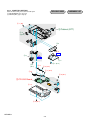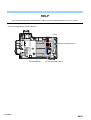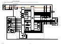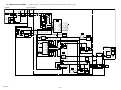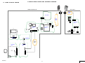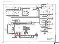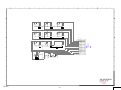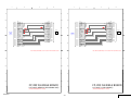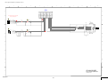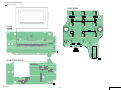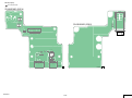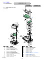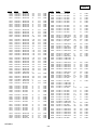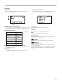
1
HVR-MRC1 SERVICE MANUAL US Model Canadian Model AEP Model E Model Chinese Model Japanese Model Ver. 1.2 2009.03 Revision History Revised-2 Replacement of the previously issued SERVICE MANUAL 9-852-266-12 with this manual. Link SPECIFICATIONS FRAME SCHEMATIC DIAGRAM REPAIR PARTS LIST SERVICE NOTE SCHEMATIC DIAGRAMS ADJUSTMENTS DISASSEMBLY PRINTED WIRING BOARDS INSTRUCTION MANUAL BLOCK DIAGRAMS The components identified by mark 0 or dotted line with mark 0 are critical for safety. Replace only with part number specified. Les composants identifiés par une marque 0 sont critiques pour la sécurité. Ne les remplacer que par une pièce portant le numéro spécifié. MEMORY RECORDING UNIT HVR-MRC1 9-852-266-13 Sony EMCS Co. 2009C0500-1 © 2009.3 Published by Kohda TEC ENGLISH JAPANESE SPECIFICATIONS General System File system CompactFlash File format Power requirement FAT32 133x 2 GB or more The capacity is the value when 1 GB equals 1 billion bytes. The actual usable capacity may be slightly less because administrative files etc. are included. HDV recording MPEG-2TS (.m2t) DVCAM/DV recording AVI-Type1 (.AVI) RAW DV (.DV) Power consumption Operating temperature Storage temperature Operating humidity DC 7.2 V (battery pack) DC 8.4 V (AC adaptor) 2.2 W 0 °C to 40 °C (32 °F to 104 °F) –20 °C to +60 °C (–4 °F to +140 °F) 20 % (20 °C) to 90 % (35 °C) (no condensation) Dimensions HVR-MRC1 : Approx. 57 × 102 × 34 mm (2 1/4 × 4 × 1 3/8 in.) HVR-MRC1+HVRA-CR1: Approx. 77 × 106 × 51 mm (3 × 4 1/8 × 2 in.) (including the projecting parts) (w/h/d) Mass HVR-MRC1 : Approx. 130 g (4.5 oz) HVR-MRC1+HVRA-CR1: Approx. 210 g (7.4 oz) (excluding CompactFlash and battery pack) Input/output jack i.LINK (IEEE1394 6-pin connector S400) Input signal HDV recording/playback Video: MPEG-2TS 1080/60i, 30p, 24p 1080/50i, 25p Audio: 2 CH MPEG 1 Audio Layer2 Stereo (16 bit 48 kHz) (1/2 CH) 4 CH MPEG 2 Audio Layer2 Stereo (16 bit 48 kHz) (3/4 CH) DVCAM/DV recording/playback Video: DV embedded Audio: PCM digital (12/16 bit, 32k, 48k) Recordable time 2 GB Approx. 9 minutes 4 GB Approx. 18 minutes 8 GB Approx. 36 minutes 16 GB Approx. 72 minutes Optional accessories AC adaptor/charger AC-VQ1050B Battery pack NP-F570/F770/F970 Design and specifications are subject to change without notice. HVR-MRC1 —2— ENGLISH JAPANESE 概略仕様 システム ファイルシステム 録画可能時間 FAT32 コンパクトフラッシュ 133x 2 GB以上 容量は、 1 GBを10億バイトで計算し た場合の数値です。 約9 分 約18分 約36分 約72分 電源部・その他 また管理用ファイルなどを含むため、 電源電圧 実際使用できる容量は若干減少する場 合があります。 消費電力 ファイルフォーマット HDV記録時 MPEG-2TS(.m2t) 動作温度 DVCAM/DV記録時 AVI-Type1(.AVI) RAW DV(.DV) 保存温度 動作湿度 バッテリー端子入力 7.2 V DC端子入力 8.4 V 2.2 W 0 °C∼ 40 °C -20 °C∼+60 °C 20 %(20 °C)∼90 %(35 °C) (結露がないこと) 対応入力信号 HDV記録再生時 2GB 4GB 8GB 16GB 外形寸法 MPEG-2TS 1080/60i , 30p , 24p 1080/50i , 25p オーディオ:2CH MPEG1 Audio Layer2 Stereo (16bit 48KHz) (1/2CH) 4CH MPEG2 Audio Layer2 Stereo (16bit 48KHz) (3/4CH) ビデオ: HVR-MRC1: 約57×102×34 mm HVR-MRC1+HVRA-CR1: 約77×106×51 mm (最大突起部を含む) (幅/高さ/奥行き) 質量 HVR-MRC1:約130g HVR-MRC1+HVRA-CR1:約210g (コンパクトフラッシュ、 バッテリー含ま ず) i.LINK(IEEE1394 6ピンコネクター S400) 別売アクセサリー ACアダプター/チャージャー AC-VQ1050 アクセサリーキット ACCKIT-D11B バッテリーパック NP-F570/F770/ F970 入力出力端子 DVCAM/DV記録再生時 ビデオ:DV embedded オーディオ:PCMデジタル (12/16 bit,32k,48k) 本機の仕様および外観は、 改良のため予告なく変更すること がありますが、 ご了承ください。 HVR-MRC1 —3— ENGLISH SAFETY-RELATED COMPONENT WARNING!! COMPONENTS IDENTIFIED BY MARK 0 OR DOTTED LINE WITH MARK 0 ON THE SCHEMATIC DIAGRAMS AND IN THE PARTS LIST ARE CRITICAL TO SAFE OPERATION. REPLACE THESE COMPONENTS WITH SONY PARTS WHOSE PART NUMBERS APPEAR AS SHOWN IN THIS MANUAL OR IN SUPPLEMENTS PUBLISHED BY SONY. JAPANESE ATTENTION AU COMPOSANT AYANT RAPPORT À LA SÉCURITÉ! LES COMPOSANTS IDENTIFÉS PAR UNE MARQUE 0 SUR LES DIAGRAMMES SCHÉMATIQUES ET LA LISTE DES PIÈCES SONT CRITIQUES POUR LA SÉCURITÉ DE FONCTIONNEMENT. NE REMPLACER CES COMPOSANTS QUE PAR DES PIÈSES SONY DONT LES NUMÉROS SONT DONNÉS DANS CE MANUEL OU DANS LES SUPPÉMENTS PUBLIÉS PAR SONY. SAFETY CHECK-OUT After correcting the original service problem, perform the following safety checks before releasing the set to the customer. 1. 2. 3. 4. 5. 6. Check the area of your repair for unsoldered or poorly-soldered connections. Check the entire board surface for solder splashes and bridges. Check the interboard wiring to ensure that no wires are "pinched" or contact high-wattage resistors. Look for unauthorized replacement parts, particularly transistors, that were installed during a previous repair. Point them out to the customer and recommend their replacement. Look for parts which, through functioning, show obvious signs of deterioration. Point them out to the customer and recommend their replacement. Check the B+ voltage to see it is at the values specified. Flexible Circuit Board Repairing • Keep the temperature of the soldering iron around 270˚C during repairing. • Do not touch the soldering iron on the same conductor of the circuit board (within 3 times). • Be careful not to apply force on the conductor when soldering or unsoldering. Unleaded solder Boards requiring use of unleaded solder are printed with the leadfree mark (LF) indicating the solder contains no lead. (Caution: Some printed circuit boards may not come printed with the lead free mark due to their particular size.) : LEAD FREE MARK Unleaded solder has the following characteristics. • Unleaded solder melts at a temperature about 40°C higher than ordinary solder. Ordinary soldering irons can be used but the iron tip has to be applied to the solder joint for a slightly longer time. Soldering irons using a temperature regulator should be set to about 350°C. Caution: The printed pattern (copper foil) may peel away if the heated tip is applied for too long, so be careful! • Strong viscosity Unleaded solder is more viscous (sticky, less prone to flow) than ordinary solder so use caution not to let solder bridges occur such as on IC pins, etc. • Usable with ordinary solder It is best to use only unleaded solder but unleaded solder may also be added to ordinary solder. HVR-MRC1 —4— ENGLISH JAPANESE サービス,点検時には次のことにご注意下さい。 6. フレキシブルプリント基板の取扱いについて 1. 注意事項をお守りください。 サービスのとき特に注意を要する個所については, キャビネット,シャーシ,部品などにラベルや捺印で • コテ先温度を270℃前後にして行なって下さい。 • 同一パターンに何度もコテ先を当てないで下さい。 注意事項を表示しています。これらの注意書き及び取 扱説明書等の注意事項を必ずお守り下さい。 (3回以内) • パターンに力が加わらないよう注意して下さい。 2. 指定部品のご使用を セットの部品は難燃性や耐電圧など安全上の特性を 7. 無鉛半田について 無鉛半田を使用している基板には,無鉛(Lead Free)を意 持ったものとなっています。従って交換部品は,使用 されていたものと同じ特性の部品を使用して下さい。 味するレッドフリーマークがプリントされています。 (注意: 基板サイズによっては,無鉛半田を使用して 特に回路図,部品表に0印で指定されている安全上重要 な部品は必ず指定のものをご使用下さい。 いてもレッドフリーマークがプリントされて いないものがあります) 3. 部品の取付けや配線の引きまわしはもとどおりに 安全上,チューブやテープなどの絶縁材料を使用した :レッドフリーマーク 無鉛半田には,以下の特性があります。 り,プリント基板から浮かして取付けた部品がありま す。また内部配線は引きまわしやクランパによって発 • 融点が従来の半田よりも約40℃高い。 従来の半田こてをそのまま使用することは可能です 熱部品や高圧部品に接近しないよう配慮されています ので,これらは必ずもとどおりにして下さい。 が,少し長めにこてを当てる必要があります。 温度調節機能のついた半田こてを使用する場合,約 4. サービス後は安全点検を サービスのために取外したネジ,部品,配線がもとど 350℃に設定して下さい。 注意: 半田こてを長く当てすぎると,基板のパター おりになっているか,またサービスした個所の周辺を 劣化させてしまったところがないかなどを点検し,安 ン(銅箔)がはがれてしまうことがあります ので,注意して下さい。 • 粘性が強い 従来の半田よりも粘性が強いため,IC端子などが半田 全性が確保されていることを確認して下さい。 5. チップ部品交換時の注意 • 取外した部品は再使用しないで下さい。 • タンタルコンデンサのマイナス側は熱に弱いため交 ブリッジしないように注意して下さい。 • 従来の半田と混ぜて使用可能 無鉛半田には無鉛半田を追加するのが最適ですが, 従来の半田を追加しても構いません。 換時は注意して下さい。 HVR-MRC1 —5— ENGLISH 1. SERVICE NOTE JAPANESE 1-1. POWER SUPPLY DURING REPAIRS In this unit, about 10 seconds after power is supplied to the battery terminal using the regulated power supply (8.4V), the power is shut off so that the unit cannot operate. These following method is available to prevent this. Method: Use the DC input terminal. (AC power adaptor/changer (AC-VQ1050B) and DK cable). 1-2. SELF-DIAGNOSIS FUNCTION When an error occurs the following warning indicators may appear on the LCD screen. And this unit is sent error code to camera. LCD screen ERROR A:12:01 Self-diagnosis display: X:Yy:ZZ X i LINK ATA Power Supply MPEG/AVI Other Fatal Error Y Main Sub Other I: A: P: M: X: F: Self-diagnosis Code X Yy ZZ A 12 01 A 12 02 A 12 03 A I 19 12 91 ** P 12 ** P 21 01 P M 21 12 02 ** M 21 ** F 11 01 F F F 11 12 20 02 ** 01 F 21 ** F F F F X X 22 29 91 92 91 99 ** 00 ** ** 85 ** 1y 2y 9y y Physical Logical Other Y1 Y2 Y9 ZZ When error is defined in the devise, the error code of it is displayed. Corrective Action Cause Cash overflow by transfer rate delay of Be sure that the CompactFlash you are using is the recommended type. CompactFlash. The selection clip is not found. Be sure that the CompactFlash you are using is the recommended type. Reformat the CompactFlash using this unit again, after reformatting The filesystem of CompactFlash is broken. the CompactFlash using personal computer. CompactFlash recognition error Check the type you are using. Error related to i.LINK Turn this unit off and then back on. It is generated the error by the power supply Turn this unit off and then back on. control from main CPU to sub CPU. It is generated the error by the power supply control from sub CUP to each Turn this unit off and then back on. device. It could not enter to the sleep mode. Turn this unit off and then back on. The input video stream is abnormal. Turn this unit off and then back on. The recording animation could not Turn this unit off and then back on. correctly treat. Communication abnormality between Turn this unit off and then back on. CompactFlash and main CPU. i.LINK error. Turn this unit off and then back on. It abnormal is generated by the file system. Reformat the CompactFlash using this unit. Reset failure of PHY (Physical Layer) There is particularly no solution Main CPU cannot be communicated with Turn this unit off and then back on. sub CPU. Sub CPU cannot control each device. Turn this unit off and then back on. Sub CPU farm is not written. Turn this unit off and then back on. Fatal error of originating hardware. Turn this unit off and then back on. Fatal error of originating software. Turn this unit off and then back on. Reception buffer overflow. Turn this unit off and then back on. Error code of main CPU firmware. Turn this unit off and then back on. Note: ** is arbitrary value. HVR-MRC1 1-1 ENGLISH JAPANESE 1-1. 修理時の電源供給について 本機では,安定化電源(8.4Vdc)からバッテリ端子に電源を供給した場合,約 10 秒後にシャットオフし,動作しなくなります。 これを避けるため,下記の方法を用いてください。 方法: DC入力端子を使用する。(ACアダプタ/チャージャ(AC-VQ1050)とDKケーブルを使用する。) 1-2. 自己診断機能 エラーが発生した場合は,エラー内容に合わせて LCD 画面にエラーコードが表示されます。 また,カメラ側にエラーコードが送信されます。 LCD画面 ERROR A:12:01 自己診断表示:X:Yy:ZZ Y X i.LINK I: ATA 電源 MPEG/AVI その他 致命的なエラー A: P: M: X: F: メイン サブ その他 自己診断コード ZZ y 1y 2y 9y フィジカル Y1 ロジカル その他 Y2 Y9 デバイスにエラーの 規定があれば,その コードを表示する。 対処 原因 X Yy ZZ A 12 01 コンパクトフラッシュの転送速度遅延に 使用のコンパクトフラッシュが推奨のカードか確認する。 よるキャッシュオーバーフロー。 A 12 02 選択クリップが見つからない。 A 12 03 コンパクトフラッシュのファイルシステ パソコンでコンパクトフラッシュのフォーマットを行った 後,本機で再度コンパクトフラッシュのフォーマットを行 ムが壊れている。 う。 A 19 91 コンパクトフラッシュ認識エラー。 電源を切り,再度電源を入れ直す。 I 12 ** i.LINK関連のエラー。 電源を切り,再度電源を入れ直す。 使用のコンパクトフラッシュが推奨のカードか確認する。 P 12 ** メインCPUからサブCPUへの電源制御で 電源を切り,再度電源を入れ直す。 エラー発生。 P 21 01 サブCUPから各デバイスへの電源制御で エラー発生。 電源を切り,再度電源を入れ直す。 P 21 02 スリープモードに入れなかった。 電源を切り,再度電源を入れ直す。 M 12 ** 入力ビデオストリーム異常。 電源を切り,再度電源を入れ直す。 M 21 ** 記録動画を正しく処理できなかった 電源を切り,再度電源を入れ直す。 F 11 01 コンパクトフラッシュ−メインCPU間通 電源を切り,再度電源を入れ直す。 信異常。 F 11 02 i.LINKエラー。 電源を切り,再度電源を入れ直す。 F 12 ** ファイルシステムで異常発生。 本機でコンパクトフラッシュのフォーマットを行う。 F 20 01 PHY(Physical Layer)のリセット失敗。 電源を切り,再度電源を入れ直す。 F 21 ** メインCPUがサブCPUとの通信ができな い。 電源を切り,再度電源を入れ直す。 F 22 ** サブCPUが各デバイスを制御できない。 電源を切り,再度電源を入れ直す。 F 29 00 サブC P U ファームが書き込まれていな 特になし い。 F 91 ** ハードウェア起因の致命的なエラー。 電源を切り,再度電源を入れ直す。 F 92 ** ソフトウェア起因の致命的なエラー。 電源を切り,再度電源を入れ直す。 X 91 85 受信バッファオーバーフロー。 電源を切り,再度電源を入れ直す。 ** メインCPUファームウェアのエラーコー 電源を切り,再度電源を入れ直す。 ド。 X 99 注:** は任意の値。 HVR-MRC1 1-2E 2. DISASSEMBLY NOTE FOR REPAIR • Make sure that the flat cable and flexible board are not cracked of bent at the terminal. Do not insert the cable insufficiently nor crookedly. • When remove a connector, don’t pull at wire of connector. It is possible that a wire is snapped. • When installing a connector, don’t press down at wire of connector. It is possible that a wire is snapped. HVR-MRC1 2-1 Cut and remove the part of gilt which comes off at the point. (Be careful or some pieces of gilt may be left inside) 2-1. IDENTIFYING PARTS Memory Recording Unit CF Base Cabinet ⋅ FP-202 Flexible Board CF Main Cabinet ⋅ CF-110 Board ⋅ FP-201 Flexible Board ⋅ LC-095 Board ⋅ TK-071 Board CF Door ⋅ SW-525 Board - DISASSEMBLY FLOW 2-2-1. BASE CABINET SECTION ⋅ CF Base Cabinet ⋅ TK-071 Board 2-2-2. MAIN CABINET SECTION ⋅ CF-110 Board ⋅ LCD Block ⋅ SW-525 Board i.LINK Cradle Cabinet (BATT) Cabinet (CF) ⋅ CR-090 Board - DISASSEMBLY FLOW 2-2-3. ADAPTOR SECTION ⋅ CR-090 Board ⋅ Cabinet (BATT) HVR-MRC1 2-2 HELP 2-2. DISASSEMBLY EXPLODED VIEW HARDWARE LIST 2-2-1. BASE CABINET SECTION Follow the disassembly in the numerical order given. 1 CF Base Cabinet (1-1 to 1-4) 2 TK-071 Board (2-1 to 2-5) 1-1 (#53) 1 CF Base Cabinet 1-4 2-2 2-1 (#46) 2 TK-071 Board 2-5 2-4 1-2 (Claw) Main Cabinet Section (See Page 2-4) 2-3 1-3 (Claw) HVR-MRC1 2-3 2-2-2. MAIN CABINET SECTION EXPLODED VIEW Follow the disassembly in the numerical order given. HARDWARE LIST 1 CF-110 Board (1-1 to 1-5) 2 LCD Block (2-1 to 2-2) 3 SW-525 Board (3-1 to 3-9) 1-2 (#46) 1-3 (#11) 1-5 1 CF-110 Board C F -1 10 2-1 1-1 2 LCD Block 3-7 (#11) 3-3 (#11) Note: Don't touch grease. A 3-6 (#46) 3-8 3 SW-525 Board Note: On installation of the SW-525 board, adjust the position of switch of CF door and S7010 of SW-525 board. S -5 W 3-1 3-4 (Boss) 25 2-2 3-2 (#2) 3-9 3-5 A 1-4 (Open) HVR-MRC1 2-4 2-2-3. ADAPTOR SECTION EXPLODED VIEW Follow the disassembly in the numerical order given. HARDWARE LIST 1 CR-090 Board (1-1 to 1-10) 2 Cabinet (BTT) (2-1 to 2-6) 1-1 (#2) 2 Cabinet (BTT) 2-5 (Open) 2-3 1-4 HELP 1-3 2-6 HELP 2-2 2-4 (#12) 2-1 (#12) 1-6 1-5 (#12) 1-7 (#12) 1-8 1-9 (#12) 1 CR-090 Board 1-10 1-2 (#12) HVR-MRC1 2-5 HELP Sheet attachment positions and procedures of processing the flexible boards/harnesses are shown. DC-IN Connector/Battery Terminal Harness Hook Battery Terminal Harness Terminal Retainer DC-IN Connector Harness HVR-MRC1 HELP 3. BLOCK DIAGRAMS Link OVERALL BLOCK DIAGRAM HVR-MRC1 POWER BLOCK DIAGRAM 3. BLOCK DIAGRAMS 3-1. OVERALL BLOCK DIAGRAM ( ) : Number in parenthesis ( ) indicates the division number of schematic diagram where the component is located. MEMORY RECORDING UNIT M3.3V 4 IC1004 RESET (5/5) 1 S7004 MENU MENU S7005 H EXEC PLAY PLAY 9 10 11 17 4 13 8 STOP MENU PLAY POR- IC4002 BUFFER (1/5) 2 MRESET_R S7007 REPEAT REPEAT 9 18 12 3 REC_ON REPEAT FF 14 7 FF 38 37 SW_PWR 6 15 8 13 5 16 SW_PWR 11 MAIN_TO_SUB 20 29 43 2 1 9 34 I2C_SDA I2C_SCL 39 SUB CPU (4/5) RESET 40 SW_OFF_CN Q7001 LED DRIVE LED_ON LCD_RESET RES DA[0] - DA[12] 512M SDRAM (3/5) 1 2 4 SUB_S_RESET C1 X5001 27MHz L1 10 30 SCL A0 CS IC3001 PWR_CF0 16 LCD_SCL LCD_A0 LCD_CS1 DDQ[0] - DDQ[31] 35 4 LCD_SDA IC2003 12 SW_OFF_CN LED_ON 20 COVER_STAT 2 S8001 COVER OPEN/CLOSE IC2004 POWER SWITCH (4/5) 2 1 C9 CLKD SO, SI, SCK ENA 4 2 6 8 10 3 12 7 32 34 35 37 42 43 44 45 26 xCD2 25 xRESET 41 SDA SCL A0 CS RES ENA ACV_UNREG SET_UNREG IC1001 DC CONTROL (5/5) SW_OFF IC5002 3.0V H3.3V M3.3V M3.3VA S3.3V P3.3V 1.8V A1.8V A : VIDEO/AUDIO SIGNAL 05 HVR-MRC1 3-1 CN6002 11 13 9 7 5 4 2 6 8 10 3 12 26 ND6001 27 38 LCD 42 39 Q6001, Q6002 LED DRIVE D6001, D6002 (BACKLIGHT) J1 CF_NDASP CARD_DETECT LCD_SDA LCD_SCL COVER_STAT ENA 15 5 21 22 14 42 LC-095 BOARD CN8003 EEPROM (2/5) XCS, XWP, XRESET COMPACT FLASH xCS0 xCS1 xIORD xIORW INTRQ IORDY xINPACK xREG xDASP xCD1 CN8004 11 13 9 7 5 18 - 20 2 - 6, 21 - 23, 27 - 31, 47 - 49 32 50 A00 - A02 PWR_CF D7009 REC LAMP, CF ACCESS Y5 Y4 C2 B1 F3 E3 E1 CN2002 SDA RESET SWITCH (4/5) 8 IC2001 D3 G1 SUB_FLMOD ON OFF xRESET COVER_STAT #RESET 39 38 34 32 28 18 16 14 12 50 MAIN CPU (2/5) CNA S7010 POWER W16, V16, T17, U20, T19, P19, N18, M18 N19, P20, T20, T18, V20, W17, Y17, V15 V10 7 m > S7008 V3 13 14 18 20 24 34 36 38 40 2 IC5001 z S7006 REC_ON W9, Y10, V9 xCD MRESET REC S7009 4 4, 6 - 9, 11 ,40 - 49 1 13, 15, 17 IC1005 RESET (5/5) xCS0 xCS1 xIORD xIORW INTRQ IORDY xINPACK xREG xDASP 3 - 12, 41, 43 - 46, 48 4 #CS0 #CS1 #DIOR #DIOW INTRQ IORDY DMARQ #DMACK A00 - A02 D00 - D15 8, 1, 2 STOP 12 REW #RESET 53 S3.3V U9 Y8 Y15 V14 Y11 W14 W15 W11 DA0 - DA2 D00 - D15 CN8001 CN8002 4, 5, 3 S7003 s STOP CN2001 CAM_LINK CNA D20, F18, E20 REW 5 LKON 3 60 C6 D7 A12 B12 E17, D19, C19 S7002 M . 16 PCLK LREQ LPS DD[1] - DD[15] CF-110 BOARD 39, 37, 35 59 SW-525 BOARD CN7001 CAM_LINK CTL0, CTL1 2 1 15 19 HDV/DV i.LINK INTERFACE (1/5) X4001 24.576MHz LD[0] - LD[7] A5, B6 HDV-i.LINK, DV-i.LINK TPA+, TPA-, TPB+, TPB- C7, A6, B7, A7, A10, A11, C11, B11 CN4002 IC4003 S7001 CAM LINK FP-201 FLEXIBLE BOARD CN4001 6 - 13 12, 11, 15, 14 6-3 15, 14, 18, 17 CN9005 CN9004 HDV-i.LINK, DV-i.LINK TPA+, TPA-, TPB+, TPB- TK-071 BOARD 4, 5 HDV/DV FP-202 FLEXIBLE BOARD CN902 HOT SHOE CN903 HOT SHOE 37 - 34 FP-203 FLEXIBLE BOARD 12, 11, 15, 14 CR-090 BOARD 15, 14, 18, 17 i.LINK CRADLE 3-2. POWER BLOCK DIAGRAM MEMORY RECORDING UNIT TK-071 BOARD FP-202 FLEXIBLE BOARD CN4002 ACV_ FB1001 F1001 UNREG UNREG R1042 F1002 S − BATT(-) 3 Q1013 Q1011 D1004 2 PWR_SUB_33 SW SIG 1 SET_UNREG BT901 BATTERY TERMINAL BATT(+) FB1002 Q1009 CN9001 + Q1012 D1003 Q1008 4 Q1007, Q1010 SW_OFF 5, 6 5, 6 CN902 HOT SHOE 6, 7 F9001 UNREG CN903 HOT SHOE 3, 4 1 2 3 CN9005 ACV_ F9002 UNREG 8, 9 PLUS MINUS_A MINUS_B 6, 7 CN9002 J901 DC IN FP-203 FLEXIBLE BOARD 3, 4 CR-090 BOARD 8, 9 i.LINK CRADLE ( ) : Number in parenthesis ( ) indicates the division number of schematic diagram where the component is located. IC2001 SUB CPU (4/5) 32 P20/ANI0 DC IN DETECT Q1003, Q1006 BATT_AD BATTERY DETECT SW-525 BOARD IB_ENABLE S7010 CN7001 SW_PWR POWER 6 15 8 13 3 18 SLEEP CN2001 SW_PWR SW_PWR ON SW_OFF_CN OFF D7009 REC LAMP, CF ACCESS R7001 Q7001 LED DRIVE 3.3V PWR_P33 P75 6 DCIN_AD 25 P27/ANI7 P124/XT2/ 41 EXCLKS PWR_LCD 26 P26/ANI6 P140/PCL/ 36 INTP6 PWR_MAIN_33 33 P130 PWR_CF0 P74 7 17 P15/TOH0 16 P16/TOH1 /INTP5 CARD_DETECT P33/TI51/ 5 TO51/INTP4 SW_OFF_CN IC2003 IC1005 RESET SWITCH (4/5) RESET (5/5) 3.3V FB1006 2 VIN VOUT 3 5 VIN FB2001 S3.3V S3.3V 4 VDD VOUT 1 POR- 2 3.3V REG (5/5) Q1004 SWITCHING L1002 IC4002 4 BUFFER (1/5) IC1002 R1025, R1026 FB1005 A1.8V 1.8V FB4005 53 IC4003 HDV/DV i.LINK INTERFACE (1/5) IC1003 Q1001 SWITCHING Q1005 CN2002 FB1003 FB1007 3.0V 5 VIN VOUT 4 L1001 3.0V CONT 1 FB1008 FB3001 FB1009 FB1010 M3.3V RESET (5/5) 4 VDD VOUT 1 05 HVR-MRC1 3-2E M RESET V3 RST- M3.3VA FB5003 IC1004 FB5004 FB5001 PWR_CF0 CARD_DETECT FB5006 4 3.3V 2 1 PWR_MAIN_33 FB5002 IC2004 POWER SWITCH (4/5) 14 CN6002 1 IC5001 IC5002 MAIN CPU (2/5) EEPROM (2/5) 14 FB6001 H3.3V PWR_CF Q1018 1 CN8004 CN8003 3.0V IC3001 512M SDRAM (3/5) PWR_LCD Q1017 ND6001 LCD CF-110 BOARD 3V REG (5/5) R1023, R1024 VDD1-VDD6 2, 8, 15, 25, 34, 40 11 12 15 18 14 LC-095 BOARD #RESET SENSE2SENSE2+ 28 RUN/SS1 SW2 BG2 13 RUN/SS2 TG2 FB4004 Q1014 Q1002 FB4002 Q1015 FB4001 Vosense2 9 P3.3V PWR_P33 FL4003 Vosense1 1 R1040 FB4003 IC1001 DC CONTROL (5/5) Q1016 FL4002 FB1004 26 22 25 30 31 FB4006 23 VIN TG1 BG1 SW1 SENSE1+ SENSE1- FL4001 R1004 CN4001 Vcc 25 Vcc 26 Vcc(A06) 27 xCD 2 FP-201 FLEXIBLE BOARD CN8002 27 26 25 50 CN8001 VCC xCD1 13 38 26 xCD2 25 R6004, Q6001, Q6002 R6005 LED DRIVE D6001, D6002 (BACKLIGHT) COMPACT FLASH 4. PRINTED WIRING BOARDS AND SCHEMATIC DIAGRAMS 4-1. FRAME SCHEMATIC DIAGRAM MEMORY RECORDING UNIT i.LINK CRADLE 1 1 FP-203 FLEXIBLE BOARD Attaching CN902 HOT SHOE 16 CN903 HOT SHOE 16 1 20 SW-525 BOARD 7 20 1 9 CN7001 5 8 20 CN9005 1 CN9004 HDV/DV CR-090 BOARD (SIDE A) 1 CN2001 1 3 6 FP-202 FLEXIBLE BOARD FLEXIBLE FLAT CABLE (FFC-157) 20 2 4 IC5002 (EEPROM) (Not supplied) 20 20 1 1 TK-071 BOARD (SIDE A) 4 CN9001 1 TK-071 BOARD (SIDE B) 1 3 CN9002 CN4002 BT901 BATTERY TERMINAL ND6001 LCD 2 1 14 1 CN4001 50 51 S CN2002 J901 DC IN 1 49 CN6002 LC-095 BOARD (SIDE A) 14 LC-095 BOARD (SIDE B) 1 FLEXIBLE FLAT CABLE (FFC-159) FLEXIBLE FLAT CABLE (FFC-159) 1 14 51 FP-201 FLEXIBLE BOARD 1 CN8003 CF-110 BOARD (SIDE A) CF-110 BOARD (SIDE B) 51 1 51 53 CN8004 26 1 2 14 1 CN8002 50 CN8001 COMPACT FLASH CONNECTOR 51 (Compact Flash) 2 49 50 54 1 25 52 05 HVR-MRC1 4-1 FRAME 4-2. SCHEMATIC DIAGRAMS Link TK-071 BOARD (1/5) (HDV/DV i.LINK INTERFACE) LC-095 BOARD (LCD) TK-071 BOARD (2/5) (MAIN CPU) SW-525 BOARD (CONTROL SWITCH) TK-071 BOARD (3/5) (SDRAM) FP-202 FLEXIBLE BOARD (HOT SHOE (MEMORY RECORDING UNIT)) TK-071 BOARD (4/5) (SUB CPU) TK-071 BOARD (5/5) (DC/DC CONVERTER) CF-110 BOARD (CF CONNECTOR) COMMON NOTE FOR SCHEMATIC DIAGRAMS HVR-MRC1 FP-203 FLEXIBLE BOARD (HOT SHOE (i. LINK CRADLE)) CR-090 BOARD (DC IN, HDV/DV CONNECTOR) 4-2. SCHEMATIC DIAGRAMS ENGLISH JAPANESE 4-2. SCHEMATIC DIAGRAMS (ENGLISH) THIS NOTE IS COMMON FOR SCHEMATIC DIAGRAMS (In addition to this, the necessary note is printed in each block) (For schematic diagrams) • All capacitors are in µF unless otherwise noted. pF : µ µF. 50 V or less are not indicated except for electrolytics and tantalums. • Chip resistors are 1/10 W unless otherwise noted. kΩ=1000 Ω, MΩ=1000 kΩ. • Caution when replacing chip parts. New parts must be attached after removal of chip. Be careful not to heat the minus side of tantalum capacitor, Because it is damaged by the heat. • Some chip part will be indicated as follows. Example C541 L452 22U 10UH TA A 2520 When indicating parts by reference number, please include the board name. The components identified by mark 0 or dotted line with mark 0 are critical for safety. Replace only with part number specified. Les composants identifiés par une marque 0 sont critiques pour la sécurité. Ne les remplacer que par une pièce portant le numéro spécifie. Kinds of capacitor External dimensions (mm) Case size • Constants of resistors, capacitors, ICs and etc with XX indicate that they are not used. In such cases, the unused circuits may be indicated. • Parts with ★ differ according to the model/destination. Refer to the mount table for each function. • All variable and adjustable resistors have characteristic curve B, unless otherwise noted. • Signal name XEDIT → EDIT PB/XREC → PB/REC • 2: non flammable resistor • 5: fusible resistor • C: panel designation • A: B+ Line • B: B– Line • J : IN/OUT direction of (+,–) B LINE. • C: adjustment for repair. (Measuring conditions voltage and waveform) • Voltages and waveforms are measured between the measurement points and ground. They are reference values and reference waveforms. (VOM of DC 10 MΩ input impedance is used) • Voltage values change depending upon input impedance of VOM used.) HVR-MRC1 4-2 4-2. SCHEMATIC DIAGRAMS ENGLISH JAPANESE (JAPANESE) 回路図共通ノート (他に必要なノートは各ブロックに記載してあります) 【回路図ノート】 0印の部品,または0印付きの点線で囲まれた部品は, 安全性を維持するために重要な部品です。 従って交換時は,必ず指定の部品を使用して下さい。 ・ケミコン,タンタルを除くコンデンサで,耐圧50V以下のもの はその耐圧を省略。単位はすべてμF(pはpF)。 ・チップ抵抗で指示のないものは,1/10W以下。 kΩ=1000Ω,MΩ=1000kΩ ・チップ部品交換時の注意 取り外した部品は再使用せず,未使用の部品をご使用くださ い。 タンタルコンデンサのマイナス側は熱に弱いため注意してくだ さい。 ・チップ部品には下記のように表示したものがあります。 例 C 541 L 452 22U 10UH TA A 2520 ↑ ↑ ↑ 種類 ケースサイズ 外形寸法(mm) ・抵抗,コンデンサ,ICなど定数にXXがあるものは,使用して いない事を示しています。このため,使用していない回路が記 載されている事があります。 ・★印のある部品は,機種などにより異なりますので機能別マウ ント一覧表を参照してください。 ・可変抵抗と半固定抵抗で,B特性の表示を省略。 ・信号名表記について,下記のような場合があります。 XEDIT → EDIT PB/XREC → PB/REC ・2は不燃性抵抗。 ・1はヒューズ抵抗。 ・Cはパネル表示名称。 ・AはB+ライン。 ・BはB−ライン。 ・JはBライン(+,−)の入出力方向を示す。 ・Cは調整名称。 お願い 図面番号で部品を指定するときは基板名又はブロック を併せて指定して下さい。 【電圧・波形測定条件ノート】 ・電圧値及び信号波形は測定点対アース間の参考値。 (デジタルマルチメータ;入力インピーダンス DC10MΩ使 用) ・使用テスタの入力インピーダンスにより電圧値が多少異なりま す。 HVR-MRC1 4-3 2 1 5 4 3 7 6 8 10 9 11 12 A A FB4001 M3.3V F 40 D00 41 xPDIAG 42 D01 43 D08 44 D02 45 D09 46 GND(xIOIS16) 47 D10 48 GND(xCD2) 49 COVER_STAT 50 GND 51 0 R4057 0 R4056 0 CTL1 GND C4001 B 25V 0.01u 33 R4036 5600 R4019 82 R4020 33 0.4 LD[0] 0.4 LD[1] 0 LD[2] #RESET 0 LD[3] 0 LD[4] R4021 82 R4022 33 R4023 22 R4024 33 R4025 33 R4026 33 R4027 XX R4028 33 DD[1] R4029 33 DD[8] R4030 33 DD[2] R4031 33 DD[9] R4032 33 DD[10] IORDY LD[5] DA2 LD[6] DMARQ DA1 0 0 0 LD[7] 0 CL4004 3.2 #DMACK DA0 R4048 LPS XX 3.3 3.3 0.1u 3.3 0 1.3 3.3 0.1u C4013 B B C4010 1.5 1.5 CTL1 D0 D1 D2 IC4003 D3 TSB41AB2PAPR HDV/DV i.LINK INTERFACE D4 D5 AGND3 TPBIAS0 D6 TPA0+ D7 TPA0- PD TPB0+ LPS TPB0- NC AGND2 FL4003 AGND5 AGND6 AVDD4 AVDD5 #RESET FILTER0 FILTER1 PLLVDD PLLGND1 PLLGND2 XI TPA10.2 TPB1+ 0.2 TPB13.3 AVDD3 1.2 R1 0 R0 CTL0 33 34 35 36 37 38 39 40 41 42 43 44 45 46 47 48 39 C4003 B 6.3V 10u TPA1+ R4069 SET_UNREG 0.1u B R4073 DD[0] R4047 10k R4042 33k DD[1] DD[8] 17 18 19 20 21 22 23 24 25 26 27 28 29 30 31 32 #PDTAG DD[2] DD[9] DD[10] XX LKON R4055 COVER_STAT R4062 6200 R4063 0 C4018 150 1u R4067 56 R1.8/P3.2 10k R4054 XX R4053 XX R4052 R4068 56 R1.8/P3.2 R1.8/P3.2 LF4001 R1.8/P0 1 5 R1.8/P0 2 6 3 7 4 8 C4019 220p B 3 1 0 R4071 R4065 56 B 0.1u C4014 0 R4072 XX CF_NDASP DD[0] SET_UNREG_CN R4070 ACV_UNREG AGND1 A00 xDASP CTL0 CNA AVDD2 38 1 1 C4017 3.3 xREG 37 CNA AGND4 AVDD1 A01 36 10k R4033 CN4002 2 4 TPBIAS1 SM A02 35 R4037 R0/P3.3 SYSCLK 1k 34 1.6 3.3 IORDY xINPACK E 33 R4050 47 PCLK 1k GND(A03) 32 LREQ R4061 xRESET 31 INTRQ LREQ R4060 GND(A04) C4016 4.7u B 6.3V R4064 56 R4066 5100 D001 NSAD500H-T1-A 4 3 2 5 1 20P 1 REG_GND 2 REG_GND 3 REG_GND 4 REG_GND 5 N.C 6 UNREG 7 UNREG 8 ACV_UNREG 9 ACV_UNREG 10 N.C 11 DETECT 12 REG_GND 13 REG_GND 14 TPA- 15 TPA+ 16 REG_GND 17 TPB- 18 TPB+ 19 REG_GND 20 REG_GND D E FP-202 FLEXIBLE LND001 – LND020 (Page 4-12) 4 2 0.1u 30 C P3.3V 4 C4015 0.1u B 3 0 B GND(xVS2) 82 FB4003 29 10k C4012 28 GND(A05) 3 1k GND(xCSEL) R4035 R4018 33k 27 FB4006 P3.3VA 2 65 64 63 62 61 60 59 58 57 56 55 54 53 52 51 50 49 C4002 B 10V 0.1u 26 Vcc(A06) #DIOR #DIOW R4059 Vcc 22 C4006 4.7u B 6.3V R4058 25 R4016 #CS1 PC2 3.3 #ISO 3.3 CPS 3.3 DVDD1 3.3 DVDD2 3.3 TESTM 0 SE D 24 Vcc 22 1 FB4004 3.3 23 INTRQ R4015 FL4001 XO 22 GND(A07) 10k C4011 12p FB4005 PC1 GND(xWE) R4034 50V CH 4 FB4002 P3.3V 3.3 21 33 #CS0 DVDD3 GND(A08) R4013 DD[7] DD[15] DVDD4 20 33 PC0 xIORW DD[15] R4012 DGND3 19 DD[7] C/LKON 18 GND(A09) 33 33 3 DD[14] DGND2 17 xIORD R4010 R4011 DD[13] DD[6] X4001 24.576MHz 1 2 25V 50V B C4008 CH 12p 0 16 DD[14] C4007 0.01u C4009 0.1u B GND(xVS1) GND(xATA_SEL) DD[6] XX NC GND(A10) 15 33 33 R4046 DD[5] C4005 0.1u DGND4 14 R4008 R4009 DD[12] 1k XX DGND1 CF-110 CN8002 Through the FP-201 Flexible (Page 4-9) 13 xCS1 DD[13] R4051 R4049 1 xCS0 DD[5] 10V B 3.3 2 12 33 33 DD[4] 3 11 D15 R4006 R4007 3.3 4 D07 33 DD[12] R4045 XX 5 9 10 DD[4] R4005 8 D06 D14 33 POR- 6 7 R4004 DD[3] DD[11] 7 6 D05 DD[11] 8 D12 DD[3] B 3.3 9 5 33 33 3.3 16 15 14 13 12 11 10 D04 R4002 R4003 XX CARD_DETECT 5 4 CARD_DETECT 3 3 D11 33 10k D03 R4001 4700 2 R4039 xCD SUB_TO_PHY R4038 1 D13 C IC4002 TC7S08FU(TE85R) BUFFER R4044 GND 4 51P H3.3VVV B R4043 10k 1 CN4001 2 R4040 S3.3V 100k H3.3V F FL4002 XX GND G G TK-071 BOARD (1/5) HDV/DV i.LINK INTERFACE H H XX MARK:NO MOUNT NO MARK:REC/PB MODE R:REC MODE P:PB MODE 05 HVR-MRC1 4-4 TK-071 (1/5) DDQ[30] DDQ[29] DDQ[28] DDQ[27] DDQ[26] DDQ[25] DDQ[24] DDQ[23] DDQ[22] DDQ[21] DDQ[20] DDQ[19] DDQ[18] DDQ[17] DDQ[16] DDQ[15] DDQ[14] DDQ[13] DDQ[12] DDQ[11] DDQ[10] DDQ[9] DDQ[8] DDQ[7] DDQ[6] DDQ[5] DDQ[4] DDQ[3] DDQ[2] DDQ[1] DDQ[0] DDQ[31] DDQ[31] XPD2 VSS25 XPD1 VSS26 XPD0 VSS27 CLK VSS28 PLL3FILTER VSS29 PLL2FILTER VSS30 PLL1FILTER VSS31 XPA0 VSS32 XPA1 VSS33 XPA2 VDD181 XPWR- IC5001 IND60C32A MAIN CPU VDD182 XPRD- VDD183 XPCS- VDD184 XPRINT VDD185 UART_RX VDD186 UART_TX VDD187 SDA VDD188 SCL VDD189 GPIO0 VDD1810 GPIO1 VDD1811 GPIO2 VDD1812 GPIO3 VDD331 GPIO4 VDD332 GPIO5 VDD333 GPIO6 VDD334 GPIO7 VDD335 RST- VDD336 LINKON VDD337 PINT VDD338 PCLK VDD339 LPS VDD3310 LREQ VDD3311 CTL0 VDD3312 CTL1 VDD3313 LCLK VDD3314 ATAEN VDD3315 PDIAG- VDD3316 IORDY VDD3317 INTRQ VDD3318 DMAREQ VDD3319 RESETCS1- VDD3321 CS0- VDD3320 VDD18_PLL1 DA2 VDD18_PLL2 DA1 VDD18_PLL3 DA0 8 7 SCK VCC xRESET xWP xCS IC5002 (Note) AT45DB081B-CNU AT45DB081D-SU 6 1 2 3 4 3.2 SO GND SI 0.8 B 3.2 0 EEPROM C5032 0.1u X5001 27MHz R5046 100 3 2 FB5005 C5027 220p 50V B XX C5029 XX C 4 1 C5031 0.1u B 10V C5026 B 10V C5034 0.1u B 10V JL5008 VCC R5038 R5036 10k 10k JL5009 RXD JL5010 VSS D JL5011 TXD I2C_SDA I2C_SCL MAIN_TO_SUB SUB_S_RESET R5029 XX R5030 XX R5031 XX R5032 XX R5033 XX R5035 C5028 0.01u 1k R5027 4700 R5028 0 LCD_CS1 LCD_RESET LCD_A0 LCD_SCL LCD_SDA SUB_FLMOD E MRESET_R LKON PCLK LPS LREQ CTL0 CTL1 CL5043 R5034 33k #PDTAG IORDY F INTRQ DMARQ #RESET #CS1 #CS0 DA2 DA1 DA0 #DMACK #DIOR G DIOW- DD0 DD1 DD2 DD3 DD4 DD5 DD6 DD7 DD8 DD9 DD10 DD11 DD12 DD13 DD14 DD15 LD0 LD1 LD2 LD3 LD4 LD5 LD6 LD7 AV4_VALID AV4_SOP AV4_SOF AV4_DATA AV4_CLK AV3_DREQ AV3_SOF AV3_IRC AV3_DATA7 AV3_VALID AV3_DATA6 AV3_SOP AV3_DATA5 DD[0] DD[1] DD[2] DD[3] DD[4] DD[5] DD[6] DD[7] DD[8] DD[9] DD[10] DD[11] DD[12] DD[13] DD[14] DD[15] LD[0] LD[1] LD[2] LD[3] LD[4] LD[5] LD[6] XX R5026 LD[7] XX #DIOW R5025 AV3_DATA4 4700 R5023 AV3_DATA3 AV3_DATA2 4700 XX R5014 R5021 XX R5013 XX XX R5012 4700 XX R5011 U1 T4 U2 H2 R3 W3 Y3 W4 V4 U5 B11 C11 A11 A10 A7 B7 A6 C7 V15 Y17 W17 V20 T18 T20 P20 N19 M18 N18 P19 T19 U20 T17 V16 W16 V14 R5020 XX R5010 J4 R5019 XX R5009 J2 4700 XX R5008 P3 N3 N1 K3 K2 J1 R5018 XX R5007 XX XX R5006 R5017 XX R5005 XX XX R5004 XX XX R5003 R5015 XX R5002 R5016 XX R5001 B16 A16 C16 B13 C13 A14 B14 C14 A15 B15 D14 C15 L19 L18 M20 K20 K18 J20 J19 J17 H19 G20 F20 L20 T3 AV3_DATA1 DIORAV3_DATA0 DMACK- VDD33A AV3_CLK VDD18A 0 C5033 0.001u XPD3 V5 W5 W6 Y6 V7 W7 Y7 V8 W8 V12 U12 Y13 W13 V13 Y14 U16 C19 E17 D19 D20 F18 E20 A2 XPD4 VSS23 C1 D3 Y4 Y5 C18 A20 W20 V19 W18 V17 V18 W19 Y20 M1 M2 A9 L1 XPD5 VSS22 0 3.2 E1 E3 XPD6 VSS21 JL5007 GND Note: Two interchangeable kinds of IC are used for IC5002. It is included in TK-071 complete board though neither of these are supplied. Y15 W11 W9 Y10 V9 U9 Y8 V10 W15 Y11 W14 M19 Y18 C12 B6 A5 D7 A12 C6 D12 B12 V3 G1 C2 B1 F3 TDI TDO TMS TCK DQ31 DQ30 DQ29 DQ28 DQ27 DQ26 DQ25 DQ24 DQ23 DQ22 DQ21 DQ20 DQ19 DQ18 DQ17 DQ16 DQ15 DQ14 DQ13 DQ12 DQ11 DQ10 DQ9 DQ8 DQ7 DQ6 DQ5 DQ4 DQ3 DQ2 DQ1 DQ0 VSS20 VSS24 A 5 DDQ[30] DDQ[29] DDQ[28] DDQ[27] DDQ[26] DDQ[25] DDQ[24] DDQ[23] DDQ[22] DDQ[21] DDQ[20] DDQ[19] DDQ[18] DDQ[17] DDQ[16] DDQ[15] DDQ[14] DDQ[13] DDQ[12] DDQ[11] DDQ[10] DDQ[9] DDQ[8] DDQ[7] DDQ[6] DDQ[5] DDQ[4] DDQ[3] DDQ[2] R5024 DDQ[1] R5022 A0 CKE A1 A2 A3 A4 A5 A6 A7 A8 A9 A10 A11 A12 BA0 BA1 DQM0 DQM1 DDQ[0] DA[1] DA[0] 33 CLKE 56 CLKD DA[2] DA[3] DA[5] DA[4] DA[6] DA[7] DA[9] DA[8] DA[11] DA[10] BA0 DQM0 BA1 DQM3 DQM1 DQM2 #RAS #WE WE- DQM2 CAS- CS- RAS- VSSA VSS_PLL1 VSS_PLL2 VSS1 VSS_PLL3 VSS2 XPD7 AV1_CLK C5024 0.01u C5025 4.7u VSS19 AV1_DATA0 M3.3VA 25V B 6.3V B XPO8 AV1_DATA1 FB5003 XPD9 VSS18 AV1_DATA2 A1.8V M3.3VA XPD10 VSS17 AV1_DATA3 FB5006 C5023 0.1u XPD11 VSS16 AV1_DATA4 A1.8V XPD12 VSS15 AV1_DATA5 C5022 0.1u XPD13 VSS14 AV1_DATA6 0.001u C5020 C5021 0.1u VSS13 AV1_DATA7 C5019 0.1u FB5004 XPD14 AV1_SOF C5018 0.1u F VSS12 AV1_SOP C5017 0.1u XPD15 AV2_CLK 0.1u C5016 SCSSRESET- VSS11 AV2_DATA0 C5015 0.1u SWE- VSS9 AV2_DATA1 C5014 0.1u VSS8 VSS10 AV2_DATA2 0.1u C5012 C5013 0.1u SI AV2_DATA3 E 10k C5030 0.1u B 10V SD AV2_DATA4 C5011 0.1u 10k JL5006 VCC VSS7 AV2_DATA5 C5010 0.1u 10k JL5005 TRST VSS6 AV2_DATA6 C5009 0.1u 10k 12 JL5004 TDO TRST AV2_DATA7 C5008 0.1u R5041 K1 M4 N2 P2 R1 R2 P4 U3 V2 W1 W2 A17 C9 D5 A3 B4 C5 A4 C8 B8 A8 D9 C10 A18 D16 C17 B17 A19 B19 B20 D18 C20 E18 E19 G17 G18 G19 H18 H20 J18 K19 R20 R19 U18 U19 B5 C4 B3 B2 SCLK AV2_SOF C5007 0.1u R5040 JL5003 TDI VSS5 AV2_SOP C5006 R5039 JL5002 TCK VSS4 AV2_VALID D T2 J3 R5037 JL5001 TMS V6 T1 C5005 0.1u 0.1u G3 H3 H1 D2 E4 11 10 9 L2 C G4 F1 8 7 6 V11 Y12 D10 L4 B C3 B10 A13 B18 F19 K17 P18 Y19 W12 U7 Y2 V1 P1 G2 N20 R18 Y16 Y1 Y9 U15 U10 U6 R17 R4 L17 K4 F17 F4 D15 D11 D6 U17 U13 U8 U4 N17 N4 M12 M11 M10 M9 L12 L11 L10 L9 K12 K11 K10 K9 J12 J11 J10 J9 H17 H4 D17 D13 D8 D4 A1 M17 VSS3 P17 U14 W10 B9 M3 L3 U11 D1 E2 F2 DQM3 C5001 4.7u B 6.3V C5002 10u B 6.3V C5003 10u B 6.3V C5004 B 4.7u 6.3V A #CAS #CS GND DA[12] M3.3V 1.8V AV1_VALID FB5001 1.8V G 5 4 3 FB5002 CLKD 2 1 M3.3V TK-071 BOARD (2/5) H DD[0] DD[1] DD[2] DD[3] DD[4] DD[5] DD[6] DD[7] DD[8] DD[9] DD[10] DD[11] DD[12] DD[13] DD[14] XX MARK:NO MOUNT NO MARK:REC/PB MODE DD[15] LD[0] LD[1] LD[2] LD[3] LD[4] LD[5] LD[6] LD[7] CL5019 CL5018 CL5017 CL5016 CL5015 CL5014 CL5013 CL5012 CL5011 CL5010 CL5009 CL5008 CL5007 CL5006 CL5005 CL5004 CL5003 CL5002 CL5001 MAIN CPU H 05 HVR-MRC1 4-5 TK-071 (2/5) 1 2 3 4 5 6 A A M3.3V 512M SDRAM IC3001 GND DA[1] DA[1] DA[2] DA[2] B DA[3] DA[3] DA[4] DA[4] DA[5] DA[5] DA[6] DA[6] DA[7] DA[7] DA[8] DA[8] DA[9] DA[9] DA[10] DA[10] BA0 BA1 DDQ[0] DDQ[0] DDQ[1] DDQ[1] C DDQ[2] DDQ[2] DDQ[3] DDQ[3] DDQ[4] DDQ[4] DDQ[5] DDQ[5] DDQ[6] DDQ[6] DDQ[7] DDQ[7] DDQ[8] DDQ[8] DDQ[9] DDQ[9] DDQ[10] DDQ[10] DDQ[11] DDQ[11] DDQ[12] DDQ[12] DDQ[13] DDQ[13] DDQ[14] DDQ[14] D DDQ[15] DDQ[15] DDQ[16] DDQ[16] DDQ[17] DDQ[17] DDQ[18] DDQ[18] DDQ[19] DDQ[19] DDQ[20] DDQ[20] DDQ[21] DDQ[21] DDQ[22] DDQ[22] DDQ[23] DDQ[23] DDQ[24] DDQ[24] DDQ[25] DDQ[25] DDQ[26] DDQ[26] E DDQ[27] DDQ[27] DDQ[28] DDQ[28] DDQ[29] DDQ[29] DDQ[30] DDQ[30] DDQ[31] DDQ[31] A0 VSSQ A1 VSSQ A2 VSSQ A3 VSSQ A4 VSSQ A5 VSSQ A6 VSSQ A7 VSSQ A8 VSSQ A9 VSSQ A10 VSS BA0 VSS BA1 VSS DQ0 VSS DQ1 VDDQ DQ2 VDDQ DQ3 VDDQ DQ4 VDDQ DQ5 VDDQ DQ6 VDDQ DQ7 VDDQ DQ8 VDDQ DQ9 VDDQ DQ10 VDDQ DQ11 VDD DQ12 VDD DQ13 VDD DQ14 DQ15 VDD NC DQ16 NC DQ17 A11 DQ18 NC DQ19 A12 DQ20 NC DQ21 NC DQ22 CLK DQ23 CKE DQ24 CASN DQ25 RASN DQ26 WEN DQ27 CSN DQ28 DQM3 DQ29 DQM2 DQ30 DQM1 DQ31 DQM0 K9 K1 F8 F2 J8 K8 J9 K7 J2 J1 E3 E7 H3 H7 H9 K2 K3 A7 F9 L7 R7 B2 B7 C9 D9 E1 L1 M9 N9 P2 P7 A3 F1 L3 R3 B3 B8 C1 D1 E9 L9 M1 N1 P3 P8 DA[0] DA[0] E2 D3 D2 B1 C2 A1 C3 A2 A8 C7 A9 C8 B9 D8 D7 E8 R2 N3 R1 N2 P1 M2 M3 L2 L8 M7 M8 P9 N8 R9 N7 R8 H8 J7 G7 J3 H2 H1 G3 G2 G1 F3 F7 G9 G8 K4M513233C-DN75T B FB3001 M3.3V C3001 4.7u 6.3V B C3002 0.1u C3003 C3004 C3005 C3006 0.1u C 0.1u 0.1u 0.1u C3007 0.1u C3013 0.1u C3008 0.1u C3009 0.1u C3010 0.1u C3011 0.1u C3012 0.1u C3014 0.1u C3015 0.1u D E DQM0 DQM1 DQM2 DQM3 #CS #WE F #RAS #CAS CLKE F R3001 R3002 33 33 CL3003 CLKD DA[12] DA[11] G G TK-071 BOARD (3/5) H SDRAM H 05 HVR-MRC1 4-6 TK-071 (3/5) 2 1 5 4 3 8 7 6 11 10 9 12 FB2001 LCD_RESET S3.3V LCD_CS1 R2053 R2010 R2009 R2008 R2006 R2005 R2004 R2003 R2002 R2001 LCD_A0 A 33k 33k 33k 33k 33k 33k 33k 33k 33k 10V C2006 B 0.1u R2034 R2035 15 R2036 1k SW_OFF_CN 13 12 STOP 11 GND R2037 R2012 R2013 R2014 1k R2038 1k R2020 GND 9 A0 8 GND 7 CS 6 GND 5 RES 4 GND 3 ENA 2 GND 1 3.0V B CF-110 1k CN8004 Through the Flexible Flat Cable (FFC-159) (Page 4-9) 1k 1k B 0.01u R2040 33k B 0.01u B C 25V 25V C2013 25V C2012 B 0.01u 25V 25V C2011 B 25V 0.01u 25V B 25V 0.01u 25V 25V C2010 C2001 25V C2009 0.01u SW-525 CN7001 Through the Flexible Flat Cable (FFC-157) (Page 4-11) B SW_OFF 0.01u COVER_STAT R2007 220k C2008 1 R2019 B 2 SDA 10 CNA 0.01u GND GND 3.0V 1k 0.01u 3 GND 11 R2018 C2005 4 REPEAT 12 PWR_LCD C2007 MENU ENA XX 1k B 5 1k B 6 R2017 0.01u 7 GND CAM_LINK R2016 C2003 8 C2002 9 R2039 R2015 B REW PLAY #RES 3300 10 FF #CS_CN 3300 1k SCL A0 3300 14 REC_ON SDA 3300 R2011 GND 13 R2049 33k 16 R2046 33k 17 3300 R2044 33k 18 GND LED_ON 14P 14 SCL R2043 33k 3.3V GND C CN2002 19 SW_PWR B 10V C2004 B 0.1u 20 GND LCD_SCL R2041 33k GND A LCD_SDA 33k 20P 0.01u CN2001 1 5 3.2 0 C2017 R2033 3.3 3.3 3.3 3.3 3.3 0 1 0 2.5 3.3 D R2045 10k 10V B R0/P3.3 C2022 0.1u B 6.3V R2022 3300 R2021 3300 C2018 4.7u 1k CL2026 C2016 1u 10V B D R2048 0 4 B 10V 3.3 3 0.1u R2042 33k 2 IC2003 TC7S32FU(TE85R) RESET SWITCH 3.3 R2032 33k 10k R2027 R2028 10k GND C2023 0.1u 10V B P120/INTP0/EXLVI P41 P40 P124/XT2/EXCLKS RESET FLMOD P123/XT1 P25/ANI5 P70/KR0 P32/INTP3/OCD1B P26/ANI6 P27/ANI7 P10/xSCK1/TxDO SUB_S_RESET XX E 3.3 IB_ENABLE 3.3 PWR_SUB_33 0 PWR_BATT R0/P3.3 R2031 0 XX 1 1 CL2041 0.7 CL2042 SUB_FLMOD BATT_AD 2 DCIN_AD AVSS C2020 XX F JL2002 FLMOD 3.2 3.2 3.2 R0/P3.2 R1/P0.5 R1/P0.6 0 0 0 0 0 0 JL2003 CLK JL2004 RXD R2055 10k RXD JL2005 VSS TXD JL2006 RESET JL2007 DATA JL2008 TXD XX R2065 XX R2063 R2047 JL2001 VCC 0 R2023 R2064 MRESET PWR_MAIN_33 3.3 13 14 15 16 17 18 19 20 21 22 23 24 R2026 10k G XX 3.3 C2019 XX AVREF P11/SI10/RxD0 P12/SO10 P14/RxD6 CL2012 P13/TxD6 P24/ANI4 P71/KR1 R2050 0 3 2 5 C2024 XX 4 0 4 3 2 5 R2059 XX XX R2061 XX 1 R2062 XX 1 IC2004 TC7S32FU(TE85R) POWER SWITCH 3.3 REGC P23/ANI3 P72/KR2 F IC2005 P121/X1/OCD0A P73/KR3 P15/TOH0 0 P22/ANI2 SUB CPU P16/TOH1/INTP5 3.3 P21/ANI1 UPD78F0513GA(S)-8EU-E2-A 25 26 27 28 29 30 31 32 33 34 35 36 P74 P20/ANI0 P17/TI50/TO50 3.3 P122/X2/EXCLK/OCD0B 1 P75 P130 IC2001 P30/INTP1 3.3 R2056 XX P33/TI51/TO51/INTP4 P31/INTP2/OCD1A 0 2.9 R2057 XX 3 R2058 XX PWR_CF 4 1.8 PWR_P33 P63 1.3 0 P01/TI010/TO00 P62/EXSCL0 8 CL2004 CARD_DETECT P00/TI000 9 E P140/PCL/INTP6 12 11 10 SUB_TO_PHY P61/SDA0 5 0 P60/SCL0 6 3.2 I2C_SDA 7 3.2 I2C_SCL 2 VDD VSS 48 47 46 45 44 43 42 41 40 39 38 37 G XX MRESET_R 0 CF_NDASP SLEEP MAIN_TO_SUB LCD_SDA TK-071 BOARD (4/5) LCD_SCL SUB CPU H XX MARK:NO MOUNT NO MARK:REC/PB MODE R:REC MODE P:PB MODE H 05 HVR-MRC1 4-7 TK-071 (4/5) • Refer to page 4-2 (English), 4-3 (Japanese) for mark 0. 2 1 5 4 3 8 7 6 11 10 9 12 IC1002 S-812C33BPI-C4NTFG 3.3V REG 6 5 2 1 ACV_UNREG 270k 0 0 C1034 0.1u B D1004 RSX101VA-30TR R1012 VOUT 1 C1045 0.1u 3.3 C1042 1u B 10V 10V 0 IC1003 TK11130CSCL-G 3V REG 3 2.3 SW_OFF 2.8 DCIN_AD R1006 18k Q1011 R1010 1800 Q1008 RTQ035P02TR B+ SWITCH (1.4A/32V) F1002 R1042 2.3 SET_UNREG 6 5 2 1 0 1u 10V C1006 0.01u B B C1002 1u 10V C1013 10u C C1007 0.01u B B Q1003,Q1006 BATTERY DETECT 2.3 3 C1001 C1022 1u Q1006 DTA124EE-TL 0 3.3 6 5 2 1 2.7 C1035 10u Q1013 B DTC115EETL INVERTER 8 C1025 10V R1019 B 1M Q1010 DTC115TMT2L DC IN DETECT R1011 PWR_BATT BATT_AD D1006 MAZS120008SO 2 3 C1046 1u B B Q1017 RTQ035P02TR 7.2 C1036 10u 0 XX B 10V C1015 0.1u 1 3.3 3.3 R1007 120k 4 VOUT 10V 1u 7.2 5 VIN R1036 33k 2.3 Q1003 DTC144EMT2L C 0 3.3 PWR_SUB_33 PWR_LCD 7.2 0 IB_ENABLE 2.7 3 B 4 GND 3.0V FB1007 3.3 DTC115EETL INVERTER Q1009 RTQ035P02TR B+ SWITCH 4 C1014 0.1u 10V B D1005 MAZS120008SO A B SPWR R1008 51k B H3.3V B+ SWITCH 6 5 2 1 R1037 33k 0 FB1008 3.3 C1047 1u 3 Q1007 LSK3541FS8T2L DC IN DETECT R1034 1M 8 VIN NC 270k R1009 3600 VSS 4 C1005 0.01u B R1005 56k VIN GND R1033 C1012 10u 10V C 3 C1004 0.01u B 8 FB1002 8 CONT 8 FB1006 2 D1003 RSX101VA-30TR (1.4A/32V) NC 3 F1001 6 FB1001 4 A ON/OFF 5 Q1012 RTQ035P02TR 4 S3.3V 8 B+ SWITCH C PWR_CF M3.3V Q1018 RTQ035P02TR B+ SWITCH 0 B FB1009 3.3 M3.3VA C1048 3 C1037 10u 4 3.3 6 5 2 1 1u FB1010 R1045 1k PWR_MAIN_33 3 S3.3V 3.3 R1023 L1001 0.051 FB1003 S3.3V 3.3 Q1016 B+ SWITCH RTF015P02TL R1040 3.3 1 7.9 D 2.8 6 5 7 8 3.3 R1041 47k R1038 33k 4 Q1005 FDS6986AS SWITCHING D 2 4.7uH SENSE2- 10 1.8 B 3.3 Q1015 RTF015P02TL B+ SWITCH 0 9 DTC144EMT2L Q1014 INVERTER R1035 1k PWR_P33 C1039 0.1u P3.3V 3.3 33k R1039 C1049 1u E 0 1.8 B 0.6 M3.3V 33VOUT 7 ITH2 SGND 6 BG2 PGND 2.2 C1038 0.1u C1030 10u 6.3V B R1029 750 8 3.3 11 R1027 33k C1028 4.7u B R1028 10k Vosense2 12 SENSE2+ TG2 6.1 13 RUN/SS2 14 NC 3.3 2.8 15 C1018 1000p C 0.8 10V 50V BOOST2 18 17 8.2 19 E 16 NC 3.3 Q1001 DTC115TMT2L NVERTER 0.051 C1026 27p 50V CH B B 0.1u 10V C1010 6.1 0 SW2 5.1 R1002 56k D1001 RB520CS-30T2R C1016 1u 100k R1024 5.1 R1043 3.3 R1004 10 7.8 B 10V 6.8 C1008 0.1u BG1 PLLIN VIN PLLFLTR BOOST1 Vosense1 XX XX 3.3 0 CT 3.2 MRESET 3.3 1.8 VDD C1040 1u B 5 1 GND VOUT SUB XX 2 0 3 5 R1022 0 4 5 IC1004 BU4325FVE-TR 1 R1015 R1017 R1020 FCB 4 20 ITH1 3 3.5 EXTVCC 2 220k R1001 INTVCC 1 F 0.7 22 10u CL1001 IC1001 LTC3728LXCUH#TR-R5 DC CONTROL 23 C 24 C1003 SLEEP 10V B 5 21 RESET C1009 1u C1043 0.01u B F R1016 R1018 R1021 0.8 XX XX S3.3V 0 RUN/SS1 NC SENSE1+ SENSE1- NC 27 28 29 30 31 32 5 D1002 RB520CS-30T2R 1.5 B 0.1u 10V C1011 2.9 0 Q1002 DTC115TMT2L INVERTER 25V C1017 B CL1002 2 G 8 1.8 50V C1019 1000p C C1020 100p CH50V R1013 5600 C1023 0.001u B50V R1014 10k 1 SUB 3.3 1.8V C1041 1u B C1024 100p 50V CH A1.8V FB1004 1.8 L1002 4.7uH 3 4 GND VOUT CT 4 1.7 C1021 0.001u 50V B VDD 3.3 POR3.3 1.9 C1044 0.1u B 2.9 8 7 5 6 Q1004 FDS6986AS SWITCHING 0.01u 1.8 6.1 6.1 1.8 R1003 56k 33 1 PGOOD 26 2 TG1 25 100k IC1005 BU4325FVE-TR 3 SW1 RESET R1044 G R1025 0.051 R1026 0.051 FB1005 C1027 27p 50V CH 3.5 R1030 20k C1029 4.7u B R1031 16k C1031 10u 6.3V B C1032 B 4.7u C1033 B 4.7u R1032 1k TK-071 BOARD (5/5) H DC/DC CONVERTER H XX MARK:NO MOUNT NO MARK:REC/PB MODE 05 HVR-MRC1 4-8 TK-071 (5/5) 2 1 5 4 3 8 7 6 11 10 9 12 A A Note: CN8001 is not supplied, but this is included in CF-110 complete board. CN8002 CN8001 GND 1 xCD1 B D03 2 D11 27 D04 3 D12 28 D05 4 D13 29 D06 5 D14 30 D07 6 D15 31 xCS0 7 xCS1 32 A10 8 xVS1 33 xATA_SEL 34 A09 10 xIORW 35 A08 11 xWE GND 14 1 50 xCD SCL 13 2 XX R8003 XX SCL 49 R8004 XX R8005 XX R8006 XX R8007 XX R8008 XX R8009 XX R8010 XX R8011 XX R8012 XX R8013 XX 36 R8015 XX R8016 XX R8017 XX R8018 XX R8019 XX D03 GND 12 3 GND D11 SDA 11 4 SDA 47 D04 GND 46 D12 45 D05 44 D13 CN6002 Through the Flexible Flat Cable (FFC-159) 43 D06 (Page 4-10) 42 41 10 5 GND A0 9 6 A0 GND 8 7 GND CS 7 8 CS GND 6 9 GND D14 RES 5 10 RES D07 GND 4 11 GND 40 D15 ENA 3 12 ENA 39 xCS0 GND 2 13 GND 38 xCS1 3.0V 1 14 3.0V 37 GND(A10) 36 GND(xVS1) 35 xATA_SEL 34 xIORD 33 GND(A09) 32 xIORW 31 GND(A08) 30 GND(xWE) 29 GND(A07) A07 12 37 28 INTRQ Vcc 13 27 Vcc Vcc 38 26 Vcc A06 14 25 Vcc(A06) 24 GND(xCSEL) xCSEL 39 A05 15 23 GND(A05) xVS2 40 22 GND(xVS2) A04 16 21 GND(A04) 20 xRESET 19 GND(A03) 18 IORDY 17 A02 16 xINPACK 15 A01 14 xREG 13 A00 12 xDASP 11 D00 10 xPDIAG xRESET 41 A03 17 IORDY 42 A02 18 43 xINPACK 19 A01 xREG 44 A00 20 xDASP 45 D00 21 46 xPDIAG D01 22 D08 47 D02 23 D09 48 D10 49 xCD2 25 GND 50 XX R8022 XX R8023 XX R8024 XX R8025 XX R8026 XX R8027 XX R8028 XX R8029 XX R8030 XX R8031 XX R8032 XX R8033 XX R8034 XX R8036 XX CL8003 R8037 XX 52 54 R8021 24 xIOIS16 53 CL8002 R8038 XX GND 48 INTRQ D E R8002 CL8001 9 xIORD COMPACT FLASH XX CN8004 14P GND 9 D01 8 D08 7 D02 6 D09 5 GND(xIOIS16) 4 D10 3 GND(xCD2) 2 COVER_STAT 1 GND LC-095 3.0V B TK-071 (4/5) CN2002 Through the Flexible Flat Cable (FFC-159) (Page 4-7) 14P CN8003 C TK-071 (1/5) CN4001 Through the FP-201 Flexible (Page 4-4) GND D E 51 C 26 51P 51 R8001 GND F S8001 COVER OPEN/CLOSE 1 3 C F 2 4 D8001 C8001 0.01u EDZ-TE61-5.6B G G CF-110 BOARD H CF CONNECTOR H XX MARK:NO MOUNT 05 HVR-MRC1 4-9 CF-110 1 2 4 3 5 6 8 7 9 10 11 12 A A CL6030 FB6001 B B R6007 300k R6008 390 R6009 150k R6010 510k C6012 10u C6013 0.1u C B GND 5 A0 6 GND 7 CS R6001 R6003 XX XX 8 GND 9 RES 10 GND 11 ENA 12 GND 13 3.0V Q6002 RTF015P02TL 3 3 R6024 33k 0 0 DTC144EMT2L Q6001 ENA 0.1u 470 CL-271TLY-C-TS D6002 R6005 C6002 470 1u Q6001, Q6002 LED DRIVE 3.3 C6001 R6004 D6001 CL-271TLY-C-TS D6001, D6002 (BACKLIGHT) R6013 33k R6014 33k 16V C 10V B 10V B C6003 1u C6004 0.1u C6005 0.1u C6006 0.1u C6007 0.1u B B B 14 C6008 1u D C C6009 1u C6010 1u C C6011 1u C C SDA SCL E R6015 33k R6016 33k R6017 33k R6018 33k R6019 33k R6020 33k R6021 33k R6022 33k A0 #RES R6023 #CS CL6001 F CL6002 CL6003 CL6004 CL6005 CL6006 33k 1 4 2 SDA 33k VDD1 3 3 33k R6012 P/S 4 GND R6011 C86 5 (Page 4-9) 2 VSS2 6 CN8003 Through the Flexible Flat Cable (FFC-159) 1 SCL CLS 7 CF-110 GND M/S 8 C 14P VDD2 9 CN6002 VR 49 48 47 46 45 44 43 42 41 40 39 38 37 36 35 34 33 32 31 30 29 28 27 26 25 24 23 22 21 20 19 18 17 16 15 14 13 12 11 10 ND6001 VSS V5 LCD C V4 V3 V2 V1 VDD3 VSS3 C2+ C2C1+ D C1C3VOUT VSS4 VSS5 VDD4 D7 D6 D5 D4 D3 D2 D1 E D0 VDD5 RD WR VSS6 A0 RES VDD6 CS2 CS1 VSS7 DOF F CL FR FRS OSC2 OSC1 G G LC-095 BOARD H H LCD XX MARK:NO MOUNT NO MARK:REC/PB MODE 05 HVR-MRC1 4-10 LC-095 1 2 5 4 3 7 6 8 10 9 11 12 A 3 3 C7008 1 2 4 1 3 H PLAY C > , , . B S7007 D7007 1 0.01u 4 B 25V 2 S7005 C7005 0.01u 3 B 25V 1 D7005 EDZ-TE61-5.6B 4 4 REPEAT MENU S7002 2 0.01u C7002 B 25V EDZ-TE61-5.6B D7002 C 2 S7008 CAM LINK C7007 0.01u 3 B 25V 1 EDZ-TE61-5.6B 4 D7008 EDZ-TE61-5.6B 3 2 S7004 1 B 25V 4 D7004 EDZ-TE61-5.6B 2 S7001 0.01u C7001 B 25V EDZ-TE61-5.6B D7001 B C7004 0.01u A EXEC CN7001 20 B 25V 2 2 4 1 3 1 z s STOP REC 2 1 D7011 XX S7010 43 5 6 R7001 330 D7009 CL-196HR-CD-T REC LAMP, CF ACCESS 3 R0/P3.3 GND 18 REPEAT 17 MENU 16 CAM_LINK 15 GND 14 FF 13 PLAY 12 REW 11 GND 10 E 7 8 4 S7009 3 D7006 EDZ-TE61-5.6B S7003 0.01u C7003 1 B 25V EDZ-TE61-5.6B 4 S7006 2 D7003 D C7006 0.01u 19 20P GND STOP 9 REC_ON 8 SW_OFF_CN 7 GND 6 SW_PWR 5 LED_ON 4 GND 3 3.3V 2 GND 1 GND D TK-071 (4/5) CN2001 Through the Flexible Flat Cable (FFC-157) (Page 4-7) E R3.3/P0 Q7001 DTA144EMT2L 3.3 POWER LED DRIVE ON T OFF F F G G SW-525 BOARD H CONTROL SWITCH H XX MARK:NO MOUNT NO MARK:REC/PB MODE R:REC MODE P:PB MODE 05 HVR-MRC1 4-11 SW-525 1 2 4 3 1 A TK-071 (1/5) CN4002 (Page 4-4) C A 1Pin 1Pin 4 3 A A B 2 1Pin 1Pin LND001 REG_GND REG_GND LND101 LND001 REG_GND REG_GND LND021 LND002 REG_GND REG_GND LND102 LND002 REG_GND REG_GND LND022 LND003 REG_GND UNREG LND103 LND003 REG_GND UNREG LND023 LND004 REG_GND UNREG LND104 LND004 REG_GND UNREG LND024 LND005 N.C ACV_UNREG LND105 LND005 N.C ACV_UNREG LND025 LND006 UNREG ACV_UNREG LND106 LND006 UNREG ACV_UNREG LND026 LND007 UNREG N.C LND107 CN902 LND007 UNREG N.C LND027 CN903 LND008 ACV_UNREG DETECT LND108 LND008 ACV_UNREG DETECT LND028 LND009 ACV_UNREG REG_GND LND109 HOT SHOE LND009 ACV_UNREG REG_GND LND029 HOT SHOE LND010 N.C N.C LND110 LND010 N.C N.C LND030 LND011 DETECT TPA- LND111 LND011 DETECT TPA- LND031 LND012 REG_GND TPA+ LND112 LND012 REG_GND TPA+ LND032 LND013 REG_GND REG_GND LND113 LND013 REG_GND REG_GND LND033 LND014 TPA- TPB- LND114 LND014 TPA- TPB- LND034 LND015 TPA+ TPB+ LND115 LND015 TPA+ TPB+ LND035 LND016 REG_GND REG_GND LND116 LND016 REG_GND REG_GND LND036 LND017 TPB- LND017 TPB- LND018 TPB+ LND018 TPB+ LND019 REG_GND LND019 REG_GND REG_GND LND020 LND020 B B CR-090 CN9005 (Page 4-13) 16Pin C C 20Pin B 16Pin C REG_GND 20Pin Note: CN902 (HOT SHOE) is not included in FP-202 flexible board. Note: CN903 (HOT SHOE) is not included in FP-203 flexible board. D D D D E E E E F F F FP-202 FLEXIBLE BOARD HOT SHOE (MEMORY RECORDING UNIT) (PRINTED WIRING BOARD is omitted) FP-203 FLEXIBLE BOARD HOT SHOE (i.LINK CRADLE) F (PRINTED WIRING BOARD is omitted) 05 05 HVR-MRC1 4-12 FP-202, FP-203 • Refer to page 4-2 (English), 4-3 (Japanese) for mark 0. 2 1 5 4 3 7 6 8 11 10 9 12 FP-203 FLEXIBLE LND001 – LND020 (Page 4-12) BT901 BATTERY TERMINAL CN9001 BATT(+) 1 SW 2 CL9001 S SIG 3 CL9002 − BATT(-) 4 REG_GND REG_GND REG_GND REG_GND N.C UNREG UNREG ACV_UNREG ACV_UNREG N.C DETECT REG_GND REG_GND TPA- TPA+ REG_GND TPB- TPB+ REG_GND REG_GND 3 4 5 6 7 8 9 10 11 12 13 14 15 16 17 18 19 20 B F9001 (1.4A/32V) FB9001 4P + 2 20P B CN9005 Note: BT901 and J901 are not included in CR-090 complete board. A 1 A C9003 0.01u B D9001 MAZS120008SO LD9002 R9002 C9004 0.01u B 0 CHASSIS_GND CN9004 LF9001 3P PLUS 1 MINUS_A 2 MINUS_B 3 C9001 1u C9002 1u 10V B 10V B TPB- 2 VG 1 VP 7 TPB+ 3 HDV/DV C 8 TH9004 9 TPA- 4 TH9003 1 CN9002 TPA+ 5 TH9002 2 J901 DC IN 6 5 C TH9001 6 RB9001 0 2 4 6 8 1 3 5 7 F9002 (1.4A/32V) 2 1 3 4 C9005 0.01u B R9003 0 D9002 MAZS120008SO LD9001 CHASSIS_GND C9006 0.01u B C9007 XX D D E E F F G G CR-090 BOARD H H DC IN, HDV/DV CONNECTOR XX MARK:NO MOUNT 05 HVR-MRC1 4-13 CR-090 4-3. PRINTED WIRING BOARDS Link TK-071 BOARD SW-525 BOARD CF-110 BOARD CR-090 BOARD LC-095 BOARD COMMON NOTE FOR PRINTED WIRING BOARDS HVR-MRC1 4-3. PRINTED WIRING BOARDS 4-3. PRINTED WIRING BOARDS (ENGLISH) THIS NOTE IS COMMON FOR PRINTED WIRING BOARDS • • : Uses unleaded solder. : Circuit board : Flexible board Pattern from the side which enables seeing. : pattern of the rear side (The other layers’ patterns are not indicated) • Through hole is omitted. • There are a few cases that the part printed on diagram isn’t mounted in this model. • C: panel designation • Chip parts. Transistor B (JAPANESE) プリント図共通ノート 【プリント図ノート】 ・ ・ :無鉛半田を使用しています。 :基板 :フレキシブル配線板 見ている面側のパターン。 :裏側のパターン (他のパターンについては表示されていません) ・スルーホールは省略。 ・プリント図には,本機で使用していない部品が記載されている 場合があります。 ・Cはパネル表示名称。 HVR-MRC1 4-14 Diode 6 5 4 4 5 6 5 C E 4 4 3 5 3 3 1 23 1 2 3 3 2 1 1 2 3 3 2 1 2 1 2 1 2 1 4 3 3 4 6 5 4 4 5 6 2 1 1 2 3 3 2 1 2 2 1 3 2 5 4 3 3 4 5 4 1 1 2 3 2 4 1 1 6 54 TK-071 (6 layers) : Uses unleaded solder. R1013 C1021 R1020 R1017 R1015 C1020 R1021 R1018 R1016 R1014 C1024 R1022 C1023 C1005 C1002 TK-071 BOARD (SIDE B) R1042 C1027 R1027 8 1 32 9 C1019 A2 B2 C2 D2 E2 F2 G2 H2 J2 K2 L2 M2 N2 P2 R2 T2 U2 V2 W2 Y2 C5021 CL5012 R5026 CL5014 R5020 R5021 R5023 R5031 R5025 C2002 C5028 R5035 R2026 R4024 R4021 R4026 R4023 R4039 R4028 R4025 R4037 R4030 R4027 R4029 R4031 R4032 R2032 12 C2017 1 48 C4018 C4016 R4072 R4073 R4062 R4063 FB1003 1 C4014 C4015 3 FL4001 2 4 FB4002 3 2 R4066 FL4002 C4019 4 Q1016 4 X4001 2 C4012 1 CL4004 C1041 FB4004 C4009 C4006 3 C1040 1 IC1004 4 5 3 1 IC1005 4 5 C5023 C3003 R4036 C3008 C3013 C3014 C3005 C3001 C3012 FB3001 R9 P9 N9 M9 L9 K9 J9 H9 G9 F9 E9 D9 C9 B9 A9 IC3001 C3002 M3.3V C3004 C3011 R3002 R3001 R4040 C2018 13 R4047 R4001 C2001 R2053 R1040 1 R4038 CL2026 3 1 IC2003 4 5 R2042 JL2006 JL2003 JL2004 JL2008 JL2002 C2007 JL2005 R2017 E C3010 C4001 R4019 CL2012 R2004 C1048 C5005 FB4001 C4003 C4002 CN4001 C5011 R4033 R4022 R2047 C2005 C5033 CL5008 C5006 R2021 R2018 2 U1 V1 W1 Y1 R2022 C2003 R2003 1 C5034 CL5009 R5019 R2019 R5029 R5030 R5033 R5032 1 R2020 R2002 FB5005 X5001 3 4 M1 N1 P1 R1 T1 CL5013 C5031 CL5011 CL5010 R2001 K1 L1 C5027 G1 H1 J1 R5018 F1 C5022 R5024 FB1008 R4020 50 U3 V3 W3 Y3 51 U4 V4 W4 Y4 M3 N3 P3 R3 T3 CL5019 M4 N4 P4 R4 T4 K3 L3 C5001 CL3003 R4013 R4018 CL5017 K4 L4 G3 H3 J3 C3007 R4011 R4015 CL5018 G4 H4 J4 F3 A1 B1 C1 D1 E1 Q1002 3 R4009 R4010 R4012 CL5015 CL5016 F4 A3 B3 C3 D3 E3 R5046 C5016 A4 B4 C4 D4 E4 C5029 JL5005 R5037 B C1044 R4007 R4008 R8 P8 N8 M8 L8 K8 J8 H8 G8 F8 E8 D8 C8 B8 A8 U5 V5 W5 Y5 C5002 FB5001 R4005 R4006 R7 P7 N7 M7 L7 K7 J7 H7 G7 F7 E7 D7 C7 B7 A7 A5 B5 C5 D5 C1043 C1015 R4003 R4004 R4016 R5039 R4054 R4055 C3015 R2033 FB2001 CL2004 R2058 C2016 JL2001 U6 V6 W6 Y6 R4053 16 R4050 R3 P3 N3 M3 L3 K3 J3 H3 G3 F3 E3 D3 C3 B3 A3 U7 V7 W7 Y7 A6 B6 C6 D6 C5008 R4034 U8 V8 W8 Y8 A7 B7 C7 D7 1 R2 P2 N2 M2 L2 K2 J2 H2 G2 F2 E2 D2 C2 B2 A2 M3.3VA R5040 R5041 E E B C E Q1003 B Q1006 R4002 R4035 R5028 17 C3009 R2056 A8 B8 C8 D8 64 R1 P1 N1 M1 L1 K1 J1 H1 G1 F1 E1 D1 C1 B1 A1 U9 V9 W9 Y9 R1008 R1007 R2038 R2037 U10 V10 W10Y10 M9 R1037 R2055 K9 L9 R4052 C4008 C5024 R2048 J9 R4058 R4056 1.8V R2045 A9 B9 C9 D9 R4059 A1.8V C5010 JL5006 JL5007 C5026 IC4003 C4011 R4057 C3006 IC5001 S C5014 J10 K10 L10 M10 R4060 FB4003 C5015 A10 B10 C10 D10 D C2023 U11 V11 W11Y11 R4061 65 C4010 C5009 J11 K11 L11 M11 G 3 IC2004 1 4 5 A11 B11 C11 D11 32 C4013 C5017 FB5003 U12 V12 W12Y12 33 FB4005 R2035 C5025 C5019 CL5043 J12 K12 L12 M12 CL5001 C5004 A12 B12 C12 D12 48 49 3 C5012 U13 V13 W13Y13 4 E Q1017 R2036 U14 V14 W14Y14 A13 B13 C13 D13 M_3.3V C1046 FB1009 C1025 C A14 B14 C14 D14 R4064 R2034 2 U15 V15 W15Y15 R4065 R4067 C5007 R2049 1 A15 B15 C15 D15 R5004 FB5006 R5005 CL5005 R5027 R1035 R1041 C1038 C1047 R4068 C4007 C1049 C B 1 C4017 R4051 S R1039 Q1014 FB1010 6 FL4003 1 4 R2046 14 U16 V16 W16Y16 R2044 C5020 A16 B16 C16 D16 CL5002 C5030 C1042 D1004 A R2043 3 2 FB4006 R1006 6 Q1009 R2041 A17 B17 C17 D17 E17 F17 G17 H17 J17 K17 L17 M17 N17 P17 R17 T17 U17 V17 W17Y17 CL5004 FB5004 G R1038 R1036 1 CN2002 A18 B18 C18 D18 E18 F18 G18 H18 J18 K18 L18 M18 N18 P18 R18 T18 U18 V18 W18Y18 R5003 4 3 R2039 R2040 CL5003 CL5007 CL5006 JL5004 JL5003 JL5001 JL5002 2 C1036 C5013 A19 B19 C19 D19 E19 F19 G19 H19 J19 K19 L19 M19 N19 P19 R19 T19 U19 V19 W19Y19 R5036 R5001 C5003 IC1003 Q1015 3 D1006 4 3 C1033 R5002 FB5002 5 1 1 FB1006 A20 B20 C20 D20 E20 F20 G20 H20 J20 K20 L20 M20 N20 P20 R20 T20 U20 V20 W20Y20 R5038 4 C1039 R5034 R4048 R5022 JL5011 JL5010 JL5009 JL5008 R4042 D 6 C1045 6 4 R1045 Q1018 Q1008 FB1004 R5007 R5017 R5012 R5009 R5014 C5018 R5016 1 R1019 C1037 C1035 R1005 C1014 6 4 IC1002 1 3 1 1 C1032 R5008 R5010 R5006 R5013 R5011 R4045 FB1005 8 4 E Q1004 C1029 R5015 IC5002 R1002 R1009 A D1003 KK E R4046 R4044 C5032 R4043 R1026 R1003 R1001 C1034 C 5 L1002 3 8 B R1025 Q1010 C1031 R4049 C4005 4 5 4 3 Q1001 R1004 1 B C1022 R1012 IC4002 R1043 C C1008 B CL1001 C1012 C1009 C1003 C1011 K D1001 A A D1002 K C1030 5 1 R1044 1 C CL1002 17 6 3 R1034 B R1033 C Q1011 C R1024 4 8 25 24 E 8 Q1013 R4071 5 L1001 4 R1011 R4070 5 4 3 LF4001 1 5 D001 1 Q1005 R1023 C1017 16 C1010 Q1012 D G S Q1007 1 C1016 C1006 C1013 FB1002 R1010 4 C1028 33 IC1001 C1018 C1007 D1005 FB1001 1 CN4002 20 R1030 C1026 F1002 F1001 R4069 R1031 R1028 FB1007 TK-071 BOARD (SIDE A) C1004 C1001 R1032 R1029 C2022 R2057 20 R2014 R2009 R2013 C2010 24 C2006 R2027 3IC2005 1 4 5 JL2007 C2024 R2059 36 C2012 CL2041 C2013 C2019 R2010 1-874-877- 11 05 25 R2011 37 R2065 C2011 C2020 05 R2008 R2012 C2004 CN2001 R2028 R2061 R2031 IC2001 C2009 R2062 R2015 R2050 R2016 R2006 R2064 R2005 C2008 R2063 R2007 CL2042 R2023 1-874-877- 11 HVR-MRC1 4-15 TK-071 CF-110 (6 layers) : Uses unleaded solder. CF-110 BOARD (SIDE A) CF-110 BOARD (SIDE B) CN8003 14 4 2 S8001 3 1 1 COVER OPEN/CLOSE 53 CN8004 1 2 26 14 1 51 D8001 C8001 R8001 R8002 R8003 R8004 R8005 R8006 R8008 50 51 R8009 R8010 R8011 R8012 R8013 CN8002 R8007 CL8001 COMPACT FLASH CN8001 R8015 R8016 R8017 R8018 R8019 CL8002 R8021 R8022 R8023 R8024 R8025 R8026 R8027 R8028 R8029 R8030 R8033 R8034 CL8003 2 1 R8031 R8032 R8036 R8037 54 52 25 50 49 R8038 05 05 Note: CN8001 is not supplied, but this is included in CF-110 complete board. 1-874-878- 11 1-874-878- 11 HVR-MRC1 4-16 CF-110 LC-095 (6 layers), SW-525 (6 layers) : Uses unleaded solder. SW-525 BOARD 3 3 1 S7007 S7004 S7001 2 4 2 4 CAM LINK 2 REPEAT C7007 C7004 C7001 D7004 D7007 H > > 3 1 , , PLAY EXEC 3 3 1 1 S7005 S7002 4 4 2 S7008 4 2 2 C7005 C7002 C7008 D7008 D7005 D7002 REC s STOP z 3 3 1 3 1 1 S7009 S7006 S7003 ND6001 LCD 4 MENU D7001 LC-095 BOARD (SIDE A) 1 3 1 2 4 2 4 2 4 C7003 C7006 A D6001, D6002 (BACKLIGHT) D7006 D7011 E K 5 1 4 7 S7010 C 8 6 K 20 D6002 A 05 B Q7001 R7001 D6001 49 REC LAMP, CF ACCESS K 1 A D7003 D7009 POWER 1-874-879- 1 05 CN7001 OFF T ON 11 1-874-880- 11 LC-095 BOARD (SIDE B) CL6030 1 CN6002 14 E FB6001 B C6001 C6013 R6001 R6024 C C6012 G Q6002 Q6001 D S C6002 R6003 R6023 R6005 R6004 CL6002 CL6004 CL6006 R6022 R6021 CL6001 CL6003 CL6005 R6020 C6011 C6010 C6009 C6008 R6019 R6018 05 C6007 C6006 C6003 C6005 R6009 C6004 R6010 R6014 R6008 R6016 R6007 R6013 R6012 R6011 R6017 R6015 1-874-879- 11 HVR-MRC1 4-17 LC-095, SW-525 CR-090 (6 layers) : Uses unleaded solder. CR-090 BOARD (SIDE A) TH9003 TH9004 7 8 1 2 3 4 5 6 9 CN9004 CR-090 BOARD (SIDE B) TH9001 TH9002 LD9001 C9007 R9002 R9003 LD9002 20 1 CN9005 2 8 RB9001 1 7 HDV/DV D9002 F9002 C9005 C9006 F9001 D9001 C9004 FB9001 C9003 1 4 LF9001 2 CL9001 C9001 CL9002 4 1 3 C9002 3 1 CN9002 CN9001 05 1-874-881- 11 05 HVR-MRC1 4-18E 1-874-881- 11 CR-090 NOTE 5. REPAIR PARTS LIST NOTE: Characters A to Z of the electrical parts list indicate location of exploded views in which the desired part is shown. EXPLODED VIEWS Link A BASE CABINET SECTION Link HVR-MRC1 B MAIN CABINET SECTION C ADAPTOR SECTION ELECTRICAL PARTS LIST CF-110 BOARD B LC-095 BOARD B CR-090 BOARD C SW-525 BOARD B ACCESSORIES TK-071 BOARD A 5. REPAIR PARTS LIST 5. REPAIR PARTS LIST (ENGLISH) NOTE: • -XX, -X mean standardized parts, so they may have some differences from the original one. • Items marked “*” are not stocked since they are seldom required for routine service. Some delay should be anticipated when ordering these items. • The mechanical parts with no reference number in the exploded views are not supplied. • Due to standardization, replacements in the parts list may be different from the parts specified in the diagrams or the components used on the set. • CAPACITORS: uF: µF • COILS uH: µH • RESISTORS All resistors are in ohms. METAL: metal-film resistor METAL OXIDE: Metal Oxide-film resistor F: nonflammable • SEMICONDUCTORS In each case, u: µ, for example: uA...: µA... , uPA... , µPA... , uPB... , µPB... , uPC... , µPC... , uPD..., µPD... When indicating parts by reference number, please include the board name. The components identified by mark 0 or dotted line with mark 0 are critical for safety. Replace only with part number specified. Les composants identifiés par une marque 0 sont critiques pour la sécurité. Ne les remplacer que par une pièce portant le numéro spécifié. • Color Indication of Appearance Parts Example: (SILVER) : Cabinet’s Color (Silver) : Parts Color (JAPANESE) 【使用上の注意】 • ここに記載されている部品は, 補修用部品であるため, 回路図及び セットに付いている部品と異なる場合があります。 • -XX, -Xは標準化部品のため, セットに付いている部品と異なる場合 があります。 • *印の部品は常備在庫しておりません。 • コンデンサの単位でuFはμFを示します。 • 抵抗の単位Ωは省略してあります。 金 被:金属被膜抵抗。 サンキン:酸化金属被膜抵抗。 • インダクタの単位でuHはμHを示します。 • 半導体の名称でuA..., uPA..., uPB..., uPC..., uPD...等はそれぞれμ A..., μPA..., μPB..., μPC..., μPD...を示します。 • Abbreviation AR : Argentine model AUS : Australian model BR : Brazilian model CH : Chinese model CND : Canadian model EE : East European model HK : Hong Kong model J : Japanese model JE : Tourist model KR : Korea model NE : North European model HVR-MRC1 5-1 お願い 図面番号で部品を指定するときは基板名又はブロック を併せて指定してください。 0印の部品,または0印付の点線で囲まれた部品は, 安全性を維持するために,重要な部品です。 従って交換時は, 必ず指定の部品を使用してください。 • 外装部品色表示 例: (SILVER):セットの色を表す。 (Silver) : 部品の色を表す。 Ver. 1.2 2009.03 The changed portions from Ver. 1.1 are shown in blue. 5. REPAIR PARTS LIST DISASSEMBLY 5-1. EXPLODED VIEWS HARDWARE LIST 5-1-1. BASE CABINET SECTION ns ns: not supplied CN902 1 #53 ns 10 #53 9 8 11 (Note) 7 Note: There are differences in the label indication in each country/area. Use the correct part for the each camera or model. (See the chart below) #46 Note: 仕向によりラベル表示に相違があります。 下表を参照してカメラ本体の機種名・仕向に 合った部品を使用してください。 6 Main Model Part No. Description HVR-Z7J HVR-S270J HVR-MRC1K (J) * A-1700-861-A SERVICE (HVR-MRC1 MAIN J) HVR-Z7U HVR-S270U HVR-MRC1K (US, CND) * A-1700-862-A SERVICE (HVR-MRC1 MAIN U) HVR-Z7N HVR-S270N * A-1700-863-A SERVICE (HVR-MRC1 MAIN N) HVR-Z7P HVR-S270P * A-1700-864-A HVR-Z7E HVR-S270E 5 2 4 3 SERVICE (HVR-MRC1 MAIN EP) HVR-MRC1K (AEP) * A-1700-865-A SERVICE (HVR-MRC1 MAIN KCE) HVR-Z7C HVR-S270C HVR-MRC1K (CH) * A-1700-866-A SERVICE (HVR-MRC1 MAIN C) Ref. No. Part No. Description * 1 * 1 * 1 2 3 3-295-565-01 3-295-566-01 3-295-567-01 1-965-666-11 1-835-017-11 LABEL (J), CF CAUTION (J) LABEL (U), CF CAUTION (US, CND, AEP, E) LABEL (CN), CF CAUTION (CH) FP-201 FLEXIBLE BOARD FLEXIBLE FLAT CABLE (FFC-159) 4 5 6 * 7 A-1498-040-A 3-290-970-01 X-2188-921-1 3-290-971-01 TK-071 BOARD, COMPLETE (SERVICE) SHEET, RADIATION HEAT SINK ASSY, CF SHEET (FP202) Main Cabinet Section (See page 5-3) Ref. No. 8 9 * 10 * 11 CN902 #46 #53 HVR-MRC1 5-2 Part No. Description 1-965-667-11 FP-202 FLEXIBLE BOARD X-2188-922-1 3-290-945-01 (Note) 1-818-891-31 2-660-401-11 CABINET ASSY, CF BASE LABEL, FUSE REPLACEMENT SERVICE (HVR-MRC1 MAIN) CONNECTOR, EXTERNAL (HOT SHOE) SCREW (M1.7), NEW TRU-STAR, P2 (Red) 3-080-206-21 SCREW, TAPPING, P2 (Black) Ver. 1.2 2009.03 The changed portions from Ver. 1.1 are shown in blue. 5. REPAIR PARTS LIST HARDWARE LIST DISASSEMBLY 5-1-2. MAIN CABINET SECTION #46 ns: not supplied #11 56 #11 57 C F -1 10 70 58 59 #11 #11 68 60 A 61 #46 62 55 63 54 53 S 64 -5 W 25 #11 65 #2 71 69 52 ns 51 ns 66 67 Ref. No. A Part No. Description Ref. No. Part No. 51 52 53 54 55 X-2188-920-1 X-2188-919-1 A-1490-529-A 1-835-016-11 X-2188-918-1 DOOR ASSY, CF LOCK ASSY, DOOR SW-525 BOARD, COMPLETE FLEXIBLE FLAT CABLE (FFC-157) FRAME ASSY, DOOR * 63 * 64 65 3-290-928-01 SHEET, CF DIFFUSION 3-290-926-01 FRAME, CF LCD GROUND 3-288-253-01 CABINET, CF MAIN 56 57 58 59 60 X-2188-823-1 A-1490-526-A 1-835-017-11 A-1544-473-A 3-290-930-01 FRAME ASSY, CF MAIN CF-110 BOARD, COMPLETE FLEXIBLE FLAT CABLE (FFC-159) LC-095 BOARD, COMPLETE (SERVICE) HOLDER, LCD 66 67 * 68 69 * 70 3-290-968-01 3-295-564-01 2-891-483-01 3-296-530-01 3-290-969-01 WINDOW, LCD LABEL, CF TAPE, LCD SHEET (H) FRAME (UPPER), CF DOOR GROUND * 71 #2 #11 #46 2-697-881-01 2-635-562-31 3-078-890-11 2-660-401-11 DAMPER, LCD SCREW (M1.7) (Black) SCREW, TAPPING (Silver) SCREW (M1.7), NEW TRU-STAR, P2 (Red) * 61 * 62 3-290-929-01 SHEET, CF REFLECTION 3-290-927-01 LIGHT, GUIDE HVR-MRC1 5-3 Description Ver. 1.2 2009.03 The changed portions from Ver. 1.1 are shown in blue. 5. REPAIR PARTS LIST DISASSEMBLY 5-1-3. ADAPTOR SECTION HARDWARE LIST #2 #2 ns: not supplied 112 ns #53 110 111 108 109 BT901 107 J901 105 106 #12 #12 113 #12 114 #12 #12 #1 102 104 101 103 CN903 #1 • Refer to page 5-1 for mark 0. Ref. No. Part No. Description 101 102 103 * 104 * 105 3-288-257-01 A-1490-527-A 1-965-668-11 3-290-984-01 3-290-981-01 CABINET (CF) CR-090 BOARD, COMPLETE FP-203 FLEXIBLE BOARD PLATE, SHOE RETAINER RETAINER, TERMINAL 106 * 107 108 109 110 3-290-980-01 3-290-985-01 3-290-986-01 2-664-982-01 X-2188-923-1 HOLDER, DC-IN PLATE, TRIPOD RETAINER GUIDE, TRIPOD SCREW, TRIPOD CABINET (BATT) ASSY #12 Ref. No. Part No. Description 112 * 113 * 114 0 BT901 2-890-916-01 3-290-982-01 3-290-983-01 1-694-411-31 CLAMP, CABLE PLATE (L), GROUND PLATE (R), GROUND TERMINAL BOARD, BATTERY CN903 0 J901 #1 #2 #12 1-818-890-21 1-785-247-31 2-635-562-11 2-635-562-31 3-080-204-21 CONNECTOR, EXTERNAL (HOT SHOE) CONNECTOR, DC-IN SCREW (M1.7) (Black) SCREW (M1.7) (Black) SCREW, TAPPING, P2 (Black) #53 111 2-697-897-01 COVER, DC-IN HVR-MRC1 5-4 3-080-206-21 SCREW, TAPPING, P2 (Black) Ver. 1.2 2009.03 The changed portions from Ver. 1.1 are shown in blue. CF-110 CR-090 LC-095 5-2. ELECTRICAL PARTS LIST Ref. No. Part No. Description Ref. No. A-1490-526-A CF-110 BOARD, COMPLETE ********************** (CN8001 is not supplied, but this is included in CF-110 complete board.) Part No. Description < COMPOSITION CIRCUIT BLOCK > RB9001 1-234-400-21 CONDUCTOR, NETWORK (1005X4) < THERMISTOR > < CAPACITOR > C8001 1-100-567-81 CERAMIC CHIP 0.01uF 10% TH9001 TH9002 TH9003 TH9004 25V < CONNECTOR > CN8001 (Not supplied) CONNECTOR, CF CARD * CN8002 1-820-857-81 CONNECTOR, FPC (ZIF) 51P * CN8003 1-820-336-71 CONNECTOR, FFC/FPC (ZIF) 14P * CN8004 1-820-336-71 CONNECTOR, FFC/FPC (ZIF) 14P 1-805-726-11 1-805-726-11 1-805-726-11 1-805-726-11 THERMISTOR, POSITIVE THERMISTOR, POSITIVE THERMISTOR, POSITIVE THERMISTOR, POSITIVE A-1544-473-A LC-095 BOARD, COMPLETE (SERVICE) ********************** < CAPACITOR > < DIODE > D8001 8-719-074-67 DIODE EDZ-TE61-5.6B < SWITCH > S8001 C6001 C6002 C6003 C6004 C6005 1-125-777-11 1-112-717-91 1-100-352-91 1-125-777-11 1-125-777-11 CERAMIC CHIP CERAMIC CHIP CERAMIC CHIP CERAMIC CHIP CERAMIC CHIP 0.1uF 1uF 1uF 0.1uF 0.1uF 10% 10% 20% 10% 10% 10V 6.3V 16V 10V 10V C6006 C6007 C6008 C6009 C6010 1-125-777-11 1-125-777-11 1-100-352-91 1-100-352-91 1-100-352-91 CERAMIC CHIP CERAMIC CHIP CERAMIC CHIP CERAMIC CHIP CERAMIC CHIP 0.1uF 0.1uF 1uF 1uF 1uF 10% 10% 20% 20% 20% 10V 10V 16V 16V 16V C6011 C6012 C6013 1-100-352-91 CERAMIC CHIP 1-100-966-91 CERAMIC CHIP 1-125-777-11 CERAMIC CHIP 1uF 10uF 0.1uF 20% 20% 10% 16V 10V 10V 1-786-148-11 SWITCH, PUSH (1 KEY) (COVER OPEN/CLOSE) A-1490-527-A CR-090 BOARD, COMPLETE ********************** < CAPACITOR > C9001 C9002 C9003 C9004 C9005 1-165-908-11 1-165-908-11 1-100-567-81 1-100-567-81 1-100-567-81 CERAMIC CHIP CERAMIC CHIP CERAMIC CHIP CERAMIC CHIP CERAMIC CHIP 1uF 1uF 0.01uF 0.01uF 0.01uF 10% 10% 10% 10% 10% 10V 10V 25V 25V 25V C9006 1-100-567-81 CERAMIC CHIP 0.01uF 10% 25V < CONNECTOR > * CN6002 1-820-336-71 CONNECTOR, FFC/FPC (ZIF) 14P < DIODE > < CONNECTOR > CN9001 CN9002 CN9004 CN9005 1-580-057-11 1-580-056-21 1-817-382-11 1-816-648-61 PIN, CONNECTOR (SMD) 4P PIN, CONNECTOR (SMD) 3P CONNECTOR, I-LINK (6P) (HDV/DV) FFC/FPC CONNECTOR (LIF) 20P * D6001 * D6002 6-501-573-01 DIODE CL-271TLY-C-TS (BACKLIGHT) 6-501-573-01 DIODE CL-271TLY-C-TS (BACKLIGHT) < FERRITE BEAD > FB6001 1-400-794-21 EMI FERRITE (SMD) (1608) < DIODE > < LIQUID CRYSTAL DISPLAY > * D9001 * D9002 6-501-961-01 DIODE MAZS120G08S0 6-501-961-01 DIODE MAZS120G08S0 ND6001 1-805-549-11 DISPLAY PANEL, LIQUID CRYSTAL < FUSE > 0 F9001 0 F9002 < TRANSISTOR > 1-576-406-11 FUSE, MICRO (1608) (1.4A/32V) 1-576-406-11 FUSE, MICRO (1608) (1.4A/32V) Q6001 Q6002 6-550-119-01 TRANSISTOR 6-551-067-01 TRANSISTOR < FERRITE BEAD > < RESISTOR > * FB9001 1-481-196-21 FERRITE, EMI (SMD) (3216) < LINE FILTER > * LF9001 1-457-217-21 COMMON MODE CHOKE COIL < RESISTOR > R9002 R9003 1-216-864-11 SHORT CHIP 1-216-864-11 SHORT CHIP DTC144EMFS6T2L RTF015P02TL 0 0 • Refer to page 5-1 for mark 0. HVR-MRC1 5-5 R6004 R6005 R6007 R6008 R6009 1-218-839-11 1-218-839-11 1-208-946-81 1-218-948-11 1-208-939-11 METAL CHIP METAL CHIP METAL CHIP RES-CHIP METAL CHIP 470 470 300K 390 150K 0.5% 0.5% 0.5% 5% 0.5% 1/10W 1/10W 1/16W 1/16W 1/16W R6010 R6011 R6012 R6013 1-208-952-81 1-218-971-11 1-218-971-11 1-218-971-11 METAL CHIP RES-CHIP RES-CHIP RES-CHIP 510K 33K 33K 33K 0.5% 5% 5% 5% 1/16W 1/16W 1/16W 1/16W Ver. 1.1 2008.06 The changed portions from Ver. 1.0 are shown in blue. Ref. No. Part No. LC-095 Description Ref. No. R6014 1-218-971-11 RES-CHIP 33K 5% 1/16W R6015 R6016 R6017 R6018 R6019 1-218-971-11 1-218-971-11 1-218-971-11 1-218-971-11 1-218-971-11 RES-CHIP RES-CHIP RES-CHIP RES-CHIP RES-CHIP 33K 33K 33K 33K 33K 5% 5% 5% 5% 5% 1/16W 1/16W 1/16W 1/16W 1/16W R6020 R6021 R6022 R6023 R6024 1-218-971-11 1-218-971-11 1-218-971-11 1-218-971-11 1-208-923-11 RES-CHIP RES-CHIP RES-CHIP RES-CHIP METAL CHIP 33K 33K 33K 33K 33K 5% 5% 5% 5% 0.5% 1/16W 1/16W 1/16W 1/16W 1/16W S7010 Description 1-771-731-21 SWITCH, SLIDE (POWER (ON/OFF)) < CAPACITOR > C1001 C1002 C1003 C1004 C1005 1-165-908-11 1-165-908-11 1-100-966-91 1-100-567-81 1-100-567-81 CERAMIC CHIP CERAMIC CHIP CERAMIC CHIP CERAMIC CHIP CERAMIC CHIP 1uF 1uF 10uF 0.01uF 0.01uF 10% 10% 20% 10% 10% 10V 10V 10V 25V 25V C1006 C1007 C1008 C1009 C1010 1-100-567-81 1-100-567-81 1-125-777-11 1-165-908-11 1-125-777-11 CERAMIC CHIP CERAMIC CHIP CERAMIC CHIP CERAMIC CHIP CERAMIC CHIP 0.01uF 0.01uF 0.1uF 1uF 0.1uF 10% 10% 10% 10% 10% 25V 25V 10V 10V 10V C1011 C1012 C1013 C1014 C1015 1-125-777-11 1-100-966-91 1-100-966-91 1-125-777-11 1-125-777-11 CERAMIC CHIP CERAMIC CHIP CERAMIC CHIP CERAMIC CHIP CERAMIC CHIP 0.1uF 10uF 10uF 0.1uF 0.1uF 10% 20% 20% 10% 10% 10V 10V 10V 10V 10V C1016 C1017 * C1018 * C1019 C1020 1-165-908-11 1-100-567-81 1-112-692-11 1-112-692-11 1-164-874-11 CERAMIC CHIP CERAMIC CHIP CERAMIC CHIP CERAMIC CHIP CERAMIC CHIP 1uF 0.01uF 1000PF 1000PF 100PF 10% 10% 5% 5% 5% 10V 25V 50V 50V 50V C1021 C1022 C1023 C1024 C1025 1-164-937-11 1-165-908-11 1-164-937-11 1-164-874-11 1-165-908-11 CERAMIC CHIP CERAMIC CHIP CERAMIC CHIP CERAMIC CHIP CERAMIC CHIP 0.001uF 1uF 0.001uF 100PF 1uF 10% 10% 10% 5% 10% 50V 10V 50V 50V 10V C1026 C1027 * C1028 * C1029 C1030 1-164-860-11 1-164-860-11 1-112-746-11 1-112-746-11 1-165-989-11 CERAMIC CHIP CERAMIC CHIP CERAMIC CHIP CERAMIC CHIP CERAMIC CHIP 27PF 27PF 4.7uF 4.7uF 10uF 5% 5% 10% 10% 10% 50V 50V 6.3V 6.3V 6.3V C1031 * C1032 * C1033 C1034 C1035 1-165-989-11 1-112-746-11 1-112-746-11 1-125-777-11 1-165-989-11 CERAMIC CHIP CERAMIC CHIP CERAMIC CHIP CERAMIC CHIP CERAMIC CHIP 10uF 4.7uF 4.7uF 0.1uF 10uF 10% 10% 10% 10% 10% 6.3V 6.3V 6.3V 10V 6.3V < SWITCH > C1036 C1037 C1038 C1039 C1040 1-165-989-11 1-165-989-11 1-125-777-11 1-125-777-11 1-112-717-91 CERAMIC CHIP CERAMIC CHIP CERAMIC CHIP CERAMIC CHIP CERAMIC CHIP 10uF 10uF 0.1uF 0.1uF 1uF 10% 10% 10% 10% 10% 6.3V 6.3V 10V 10V 6.3V < CAPACITOR > C7001 C7002 C7003 C7004 C7005 1-100-567-81 1-100-567-81 1-100-567-81 1-100-567-81 1-100-567-81 CERAMIC CHIP CERAMIC CHIP CERAMIC CHIP CERAMIC CHIP CERAMIC CHIP 0.01uF 0.01uF 0.01uF 0.01uF 0.01uF 10% 10% 10% 10% 10% 25V 25V 25V 25V 25V C7006 C7007 C7008 1-100-567-81 CERAMIC CHIP 1-100-567-81 CERAMIC CHIP 1-100-567-81 CERAMIC CHIP 0.01uF 0.01uF 0.01uF 10% 10% 10% 25V 25V 25V < CONNECTOR > CN7001 1-816-648-61 FFC/FPC CONNECTOR (LIF) 20P < DIODE > D7001 D7002 D7003 D7004 D7005 8-719-074-67 8-719-074-67 8-719-074-67 8-719-074-67 8-719-074-67 DIODE DIODE DIODE DIODE DIODE EDZ-TE61-5.6B EDZ-TE61-5.6B EDZ-TE61-5.6B EDZ-TE61-5.6B EDZ-TE61-5.6B D7006 D7007 D7008 D7009 8-719-074-67 8-719-074-67 8-719-074-67 8-719-077-09 DIODE DIODE DIODE DIODE EDZ-TE61-5.6B EDZ-TE61-5.6B EDZ-TE61-5.6B CL-196HR-CD-T (REC LAMP, CF ACCESS) < TRANSISTOR > 6-550-239-01 TRANSISTOR DTA144EMFS6T2L < RESISTOR > R7001 TK-071 A-1498-040-A TK-071 BOARD, COMPLETE (SERVICE) ********************** (IC5002 is not supplied, but this is included in TK-071 complete board.) A-1490-529-A SW-525 BOARD, COMPLETE *********************** Q7001 Part No. SW-525 1-208-671-11 METAL CHIP 330 0.5% 1/16W S7001 S7002 S7003 S7004 S7005 1-771-844-21 1-771-844-21 1-771-844-21 1-771-844-21 1-771-844-21 SWITCH, TACTILE (CAM LINK) SWITCH, TACTILE (., EXEC M) SWITCH, TACTILE (s STOP) SWITCH, TACTILE (MENU) SWITCH, TACTILE (H PLAY, EXEC) C1041 C1042 C1043 C1044 C1045 1-112-717-91 1-165-908-11 1-100-567-81 1-125-777-11 1-125-777-11 CERAMIC CHIP CERAMIC CHIP CERAMIC CHIP CERAMIC CHIP CERAMIC CHIP 1uF 1uF 0.01uF 0.1uF 0.1uF 10% 10% 10% 10% 10% 6.3V 10V 25V 10V 10V S7006 S7007 S7008 S7009 1-771-844-21 1-771-844-21 1-771-844-21 1-771-844-21 SWITCH, TACTILE (REC z) SWITCH, TACTILE (REPEAT) SWITCH, TACTILE (>, EXEC m) SWITCH, TACTILE (REC) C1046 C1047 C1048 C1049 C2001 1-112-717-91 1-112-717-91 1-112-717-91 1-112-717-91 1-100-567-81 CERAMIC CHIP CERAMIC CHIP CERAMIC CHIP CERAMIC CHIP CERAMIC CHIP 1uF 1uF 1uF 1uF 0.01uF 10% 10% 10% 10% 10% 6.3V 6.3V 6.3V 6.3V 25V HVR-MRC1 5-6 Ver. 1.2 2009.03 The changed portions from Ver. 1.1 are shown in blue. Ref. No. Part No. TK-071 Description Ref. No. C2002 C2003 C2004 C2005 C2006 1-100-567-81 1-100-567-81 1-125-777-11 1-100-567-81 1-125-777-11 CERAMIC CHIP CERAMIC CHIP CERAMIC CHIP CERAMIC CHIP CERAMIC CHIP 0.01uF 0.01uF 0.1uF 0.01uF 0.1uF 10% 10% 10% 10% 10% 25V 25V 10V 25V 10V C2007 C2008 C2009 C2010 C2011 1-100-567-81 1-100-567-81 1-100-567-81 1-100-567-81 1-100-567-81 CERAMIC CHIP CERAMIC CHIP CERAMIC CHIP CERAMIC CHIP CERAMIC CHIP 0.01uF 0.01uF 0.01uF 0.01uF 0.01uF 10% 10% 10% 10% 10% 25V 25V 25V 25V 25V C2012 C2013 C2016 C2017 * C2018 1-100-567-81 1-100-567-81 1-165-908-11 1-125-777-11 1-112-746-11 CERAMIC CHIP CERAMIC CHIP CERAMIC CHIP CERAMIC CHIP CERAMIC CHIP 0.01uF 0.01uF 1uF 0.1uF 4.7uF 10% 10% 10% 10% 10% 25V 25V 10V 10V 6.3V C2022 C2023 * C3001 C3002 C3003 1-125-777-11 1-125-777-11 1-112-746-11 1-125-777-11 1-125-777-11 CERAMIC CHIP CERAMIC CHIP CERAMIC CHIP CERAMIC CHIP CERAMIC CHIP 0.1uF 0.1uF 4.7uF 0.1uF 0.1uF 10% 10% 10% 10% 10% 10V 10V 6.3V 10V 10V C3004 C3005 C3006 C3007 C3008 1-125-777-11 1-125-777-11 1-125-777-11 1-125-777-11 1-125-777-11 CERAMIC CHIP CERAMIC CHIP CERAMIC CHIP CERAMIC CHIP CERAMIC CHIP 0.1uF 0.1uF 0.1uF 0.1uF 0.1uF 10% 10% 10% 10% 10% 10V 10V 10V 10V 10V C3009 C3010 C3011 C3012 C3013 1-125-777-11 1-125-777-11 1-125-777-11 1-125-777-11 1-125-777-11 CERAMIC CHIP CERAMIC CHIP CERAMIC CHIP CERAMIC CHIP CERAMIC CHIP 0.1uF 0.1uF 0.1uF 0.1uF 0.1uF 10% 10% 10% 10% 10% 10V 10V 10V 10V 10V C3014 C3015 C4001 C4002 C4003 1-125-777-11 1-125-777-11 1-100-567-81 1-125-777-11 1-165-989-11 CERAMIC CHIP CERAMIC CHIP CERAMIC CHIP CERAMIC CHIP CERAMIC CHIP 0.1uF 0.1uF 0.01uF 0.1uF 10uF 10% 10% 10% 10% 10% 10V 10V 25V 10V 6.3V C4005 * C4006 C4007 C4008 C4009 1-125-777-11 1-112-746-11 1-100-567-81 1-164-852-11 1-125-777-11 CERAMIC CHIP CERAMIC CHIP CERAMIC CHIP CERAMIC CHIP CERAMIC CHIP 0.1uF 4.7uF 0.01uF 12PF 0.1uF 10% 10% 10% 5% 10% 10V 6.3V 25V 50V 10V C4010 C4011 C4012 C4013 C4014 1-125-777-11 1-164-852-11 1-125-777-11 1-125-777-11 1-125-777-11 CERAMIC CHIP CERAMIC CHIP CERAMIC CHIP CERAMIC CHIP CERAMIC CHIP 0.1uF 12PF 0.1uF 0.1uF 0.1uF 10% 5% 10% 10% 10% 10V 50V 10V 10V 10V C4015 * C4016 C4017 C4018 C4019 1-125-777-11 1-112-746-11 1-125-777-11 1-112-717-91 1-164-933-11 CERAMIC CHIP CERAMIC CHIP CERAMIC CHIP CERAMIC CHIP CERAMIC CHIP 0.1uF 4.7uF 0.1uF 1uF 220PF 10% 10% 10% 10% 10% 10V 6.3V 10V 6.3V 50V * C5001 C5002 C5003 * C5004 C5005 1-112-746-11 1-165-989-11 1-165-989-11 1-112-746-11 1-125-777-11 CERAMIC CHIP CERAMIC CHIP CERAMIC CHIP CERAMIC CHIP CERAMIC CHIP 4.7uF 10uF 10uF 4.7uF 0.1uF 10% 10% 10% 10% 10% 6.3V 6.3V 6.3V 6.3V 10V 1-125-777-11 CERAMIC CHIP 1-125-777-11 CERAMIC CHIP 0.1uF 0.1uF 10% 10% 10V 10V Part No. Description C5008 C5009 C5010 1-125-777-11 CERAMIC CHIP 1-125-777-11 CERAMIC CHIP 1-125-777-11 CERAMIC CHIP 0.1uF 0.1uF 0.1uF 10% 10% 10% 10V 10V 10V C5011 C5012 C5013 C5014 C5015 1-125-777-11 1-125-777-11 1-125-777-11 1-125-777-11 1-125-777-11 CERAMIC CHIP CERAMIC CHIP CERAMIC CHIP CERAMIC CHIP CERAMIC CHIP 0.1uF 0.1uF 0.1uF 0.1uF 0.1uF 10% 10% 10% 10% 10% 10V 10V 10V 10V 10V C5016 C5017 C5018 C5019 C5020 1-125-777-11 1-125-777-11 1-125-777-11 1-125-777-11 1-164-937-11 CERAMIC CHIP CERAMIC CHIP CERAMIC CHIP CERAMIC CHIP CERAMIC CHIP 0.1uF 0.1uF 0.1uF 0.1uF 0.001uF 10% 10% 10% 10% 10% 10V 10V 10V 10V 50V C5021 C5022 C5023 C5024 * C5025 1-125-777-11 1-125-777-11 1-125-777-11 1-100-567-81 1-112-746-11 CERAMIC CHIP CERAMIC CHIP CERAMIC CHIP CERAMIC CHIP CERAMIC CHIP 0.1uF 0.1uF 0.1uF 0.01uF 4.7uF 10% 10% 10% 10% 10% 10V 10V 10V 25V 6.3V C5026 C5028 C5030 C5031 C5032 1-164-933-11 1-100-567-81 1-125-777-11 1-125-777-11 1-125-777-11 CERAMIC CHIP CERAMIC CHIP CERAMIC CHIP CERAMIC CHIP CERAMIC CHIP 220PF 0.01uF 0.1uF 0.1uF 0.1uF 10% 10% 10% 10% 10% 50V 25V 10V 10V 10V C5033 C5034 1-164-937-11 CERAMIC CHIP 1-125-777-11 CERAMIC CHIP 0.001uF 0.1uF 10% 10% 50V 10V < CONNECTOR > * CN2001 CN2002 * CN4001 CN4002 1-818-516-71 1-816-645-61 1-820-857-81 1-816-648-61 CONNECTOR, FFC/FPC (ZIF) 20P FFC/FPC CONNECTOR (LIF) 14P CONNECTOR, FPC (ZIF) 51P FFC/FPC CONNECTOR (LIF) 20P < DIODE > D001 0 D1001 0 D1002 D1003 D1004 6-500-750-01 6-501-272-01 6-501-272-01 6-501-124-01 6-501-124-01 DIODE DIODE DIODE DIODE DIODE NSAD500H-T1-A RB520CS-30T2R RB520CS-30T2R RSX101VA-30TR RSX101VA-30TR * D1005 * D1006 6-501-961-01 DIODE MAZS120G08S0 6-501-961-01 DIODE MAZS120G08S0 < FUSE > 0 F1001 0 F1002 1-576-406-11 FUSE, MICRO (1608) (1.4A/32V) 1-576-406-11 FUSE, MICRO (1608) (1.4A/32V) < FERRITE BEAD > C5006 C5007 * FB1001 FB1002 FB1003 FB1004 FB1005 1-481-196-21 1-400-915-21 1-400-915-21 1-400-915-21 1-400-619-11 FERRITE, EMI (SMD) (3216) INDUCTOR (EMI FERRITE) (2012) INDUCTOR (EMI FERRITE) (2012) INDUCTOR (EMI FERRITE) (2012) BEAD, FERRITE (CHIP) (1608) FB1006 FB1007 FB1008 FB1009 FB1010 1-400-619-11 1-400-619-11 1-400-619-11 1-400-331-11 1-400-619-11 BEAD, FERRITE (CHIP) (1608) BEAD, FERRITE (CHIP) (1608) BEAD, FERRITE (CHIP) (1608) FERRITE, EMI (SMD) (1005) BEAD, FERRITE (CHIP) (1608) FB2001 1-400-915-21 INDUCTOR (EMI FERRITE) (2012) • Refer to page 5-1 for mark 0. HVR-MRC1 5-7 TK-071 Ref. No. Part No. Description FB3001 FB4001 FB4002 FB4003 1-400-915-21 1-400-915-21 1-400-915-21 1-400-331-11 INDUCTOR (EMI FERRITE) (2012) INDUCTOR (EMI FERRITE) (2012) INDUCTOR (EMI FERRITE) (2012) FERRITE, EMI (SMD) (1005) Ref. No. FB4004 FB4005 FB4006 FB5001 FB5002 1-400-619-11 1-400-331-11 1-400-915-21 1-400-915-21 1-400-915-21 BEAD, FERRITE (CHIP) (1608) FERRITE, EMI (SMD) (1005) INDUCTOR (EMI FERRITE) (2012) INDUCTOR (EMI FERRITE) (2012) INDUCTOR (EMI FERRITE) (2012) FB5003 FB5004 FB5005 FB5006 1-400-915-21 1-400-331-11 1-400-331-11 1-400-915-21 INDUCTOR (EMI FERRITE) (2012) FERRITE, EMI (SMD) (1005) FERRITE, EMI (SMD) (1005) INDUCTOR (EMI FERRITE) (2012) Q1016 Q1017 Q1018 FL4001 1-234-939-21 FILTER, EMI REMOVAL (SMD) FL4002 1-234-939-21 FILTER, EMI REMOVAL (SMD) FL4003 1-234-939-21 FILTER, EMI REMOVAL (SMD) < IC > 6-707-357-01 6-709-667-01 6-704-257-01 6-710-663-01 6-710-663-01 IC IC IC IC IC LTC3728LXCUH#TR-R5 S-812C33BPI-C4NTFG TK11130CSCL-G BU4325FVE-TR BU4325FVE-TR * IC2001 IC2003 IC2004 * IC3001 IC4002 6-712-221-01 8-759-058-64 8-759-058-64 6-710-662-01 8-759-058-62 IC IC IC IC IC uPD78F0513GA (S)-8EU-E2-A TC7S32FU (TE85R) TC7S32FU (TE85R) K4M513233C-DN75T TC7S08FU (TE85R) * IC4003 * IC5001 IC5002 IC5002 6-710-683-01 6-712-220-01 (Not supplied) (Not supplied) IC IC IC IC TSB41AB2PAPR IND60C32A AT45DB081B-CNU (Note) AT45DB081D-SU (Note) * * * * < COIL > L1001 L1002 1-456-019-11 INDUCTOR 1-456-019-11 INDUCTOR Description 6-551-067-01 TRANSISTOR 6-550-354-01 TRANSISTOR 6-550-354-01 TRANSISTOR RTF015P02TL RTQ035P02TR RTQ035P02TR < RESISTOR > < FILTER > 0 IC1001 * IC1002 IC1003 * IC1004 * IC1005 Part No. 4.7uH 4.7uH < LINE FILTER > R1001 R1002 R1003 R1004 R1005 1-218-981-91 1-218-974-11 1-218-974-11 1-208-635-11 1-218-974-11 RES-CHIP RES-CHIP RES-CHIP METAL CHIP RES-CHIP 220K 56K 56K 10 56K 5% 5% 5% 0.5% 5% 1/16W 1/16W 1/16W 1/16W 1/16W R1006 R1007 R1008 R1009 R1010 1-208-713-11 1-218-978-11 1-208-928-11 1-208-696-11 1-208-893-11 METAL CHIP RES-CHIP METAL CHIP METAL CHIP METAL CHIP 18K 120K 51K 3.6K 1.8K 0.5% 5% 0.5% 0.5% 0.5% 1/16W 1/16W 1/16W 1/16W 1/16W R1012 R1013 R1014 R1015 R1019 1-218-982-11 1-208-905-11 1-208-911-11 1-218-990-81 1-218-989-11 RES-CHIP METAL CHIP METAL CHIP SHORT CHIP RES-CHIP 270K 5.6K 10K 0 1M 5% 0.5% 0.5% 1/16W 1/16W 1/16W 5% 1/16W R1021 R1023 R1024 R1025 R1026 1-218-990-81 1-245-685-21 1-245-685-21 1-245-685-21 1-245-685-21 SHORT CHIP RES-CHIP RES-CHIP RES-CHIP RES-CHIP 0 0.051 0.051 0.051 0.051 5% 5% 5% 5% 1/8W 1/8W 1/8W 1/8W R1027 R1028 R1029 R1030 R1031 1-208-923-11 1-208-911-11 1-208-884-81 1-208-918-11 1-208-712-11 METAL CHIP METAL CHIP METAL CHIP METAL CHIP METAL CHIP 33K 10K 750 20K 16K 0.5% 0.5% 0.5% 0.5% 0.5% 1/16W 1/16W 1/16W 1/16W 1/16W R1032 R1033 R1034 R1035 R1036 1-208-683-11 1-218-982-11 1-218-989-11 1-208-683-11 1-208-923-11 METAL CHIP RES-CHIP RES-CHIP METAL CHIP METAL CHIP 1K 270K 1M 1K 33K 0.5% 5% 5% 0.5% 0.5% 1/16W 1/16W 1/16W 1/16W 1/16W R1037 R1038 R1039 R1040 R1041 1-208-923-11 1-208-923-11 1-208-923-11 1-216-789-11 1-208-927-11 METAL CHIP METAL CHIP METAL CHIP METAL CHIP METAL CHIP 33K 33K 33K 2.2 47K 0.5% 0.5% 0.5% 5% 0.5% 1/16W 1/16W 1/16W 1/10W 1/16W R1042 R1043 R1044 R1045 R2001 1-216-864-11 1-218-977-11 1-218-977-11 1-218-953-11 1-208-923-11 SHORT CHIP RES-CHIP RES-CHIP RES-CHIP METAL CHIP 0 100K 100K 1K 33K 5% 5% 5% 0.5% 1/16W 1/16W 1/16W 1/16W R2002 R2003 R2004 R2005 R2006 1-208-923-11 1-208-923-11 1-208-923-11 1-208-923-11 1-208-923-11 METAL CHIP METAL CHIP METAL CHIP METAL CHIP METAL CHIP 33K 33K 33K 33K 33K 0.5% 0.5% 0.5% 0.5% 0.5% 1/16W 1/16W 1/16W 1/16W 1/16W R2007 1-208-943-11 METAL CHIP 220K 0.5% 1/16W LF4001 1-457-064-13 COMMON MODE CHOKE COIL < TRANSISTOR > Q1001 Q1002 Q1003 0 Q1004 0 Q1005 6-550-566-01 6-550-566-01 6-550-119-01 6-709-438-01 6-709-438-01 TRANSISTOR TRANSISTOR TRANSISTOR TRANSISTOR TRANSISTOR DTC115TMFS6T2L DTC115TMFS6T2L DTC144EMFS6T2L FDS6986AS FDS6986AS Q1006 Q1007 Q1008 Q1009 Q1010 8-729-928-34 6-551-346-01 6-550-354-01 6-550-354-01 6-550-566-01 TRANSISTOR TRANSISTOR TRANSISTOR TRANSISTOR TRANSISTOR DTA124EE-TL LSK3541FS8T2L RTQ035P02TR RTQ035P02TR DTC115TMFS6T2L * Q1011 Q1012 * Q1013 Q1014 Q1015 6-551-600-01 6-550-354-01 6-551-600-01 6-550-119-01 6-551-067-01 TRANSISTOR TRANSISTOR TRANSISTOR TRANSISTOR TRANSISTOR DTC115EETL RTQ035P02TR DTC115EETL DTC144EMFS6T2L RTF015P02TL Note: Two interchangeable kinds of IC are used for IC5002. It is included in TK-071 complete board though neither of these are supplied. Note: IC5002には互換性のある2種類のICが使用され ています。これらはいずれも供給されません が,マウント済みTK-071基板に含まれます。 • Refer to page 5-1 for mark 0. HVR-MRC1 5-8 TK-071 Ref. No. Part No. Description R2008 R2009 R2010 R2011 1-208-923-11 1-208-923-11 1-208-923-11 1-208-683-11 METAL CHIP METAL CHIP METAL CHIP METAL CHIP 33K 33K 33K 1K 0.5% 0.5% 0.5% 0.5% 1/16W 1/16W 1/16W 1/16W Ref. No. R2012 R2013 R2014 R2015 R2016 1-208-683-11 1-208-683-11 1-208-683-11 1-208-683-11 1-208-683-11 METAL CHIP METAL CHIP METAL CHIP METAL CHIP METAL CHIP 1K 1K 1K 1K 1K 0.5% 0.5% 0.5% 0.5% 0.5% 1/16W 1/16W 1/16W 1/16W 1/16W R2017 R2018 R2019 R2020 R2021 1-208-683-11 1-208-683-11 1-208-683-11 1-208-683-11 1-208-695-11 METAL CHIP METAL CHIP METAL CHIP METAL CHIP METAL CHIP 1K 1K 1K 1K 3.3K 0.5% 0.5% 0.5% 0.5% 0.5% 1/16W 1/16W 1/16W 1/16W 1/16W R2022 R2026 R2027 R2028 R2032 1-208-695-11 1-208-911-11 1-208-911-11 1-208-911-11 1-208-923-11 METAL CHIP METAL CHIP METAL CHIP METAL CHIP METAL CHIP 3.3K 10K 10K 10K 33K 0.5% 0.5% 0.5% 0.5% 0.5% 1/16W 1/16W 1/16W 1/16W 1/16W R2033 R2034 R2035 R2036 R2037 1-208-683-11 1-208-695-11 1-208-695-11 1-208-695-11 1-208-695-11 METAL CHIP METAL CHIP METAL CHIP METAL CHIP METAL CHIP 1K 3.3K 3.3K 3.3K 3.3K 0.5% 0.5% 0.5% 0.5% 0.5% 1/16W 1/16W 1/16W 1/16W 1/16W R2038 R2040 R2041 R2042 R2043 1-208-695-11 1-208-923-11 1-208-923-11 1-208-923-11 1-208-923-11 METAL CHIP METAL CHIP METAL CHIP METAL CHIP METAL CHIP 3.3K 33K 33K 33K 33K 0.5% 0.5% 0.5% 0.5% 0.5% 1/16W 1/16W 1/16W 1/16W 1/16W R2044 R2045 R2046 R2048 R2049 1-208-923-11 1-208-911-11 1-208-923-11 1-218-990-81 1-208-923-11 METAL CHIP METAL CHIP METAL CHIP SHORT CHIP METAL CHIP 33K 10K 33K 0 33K 0.5% 0.5% 0.5% 1/16W 1/16W 1/16W 0.5% 1/16W R2053 R2055 R2064 R3001 R3002 1-208-923-11 1-208-911-11 1-218-990-81 1-208-647-11 1-208-647-11 METAL CHIP METAL CHIP SHORT CHIP METAL CHIP METAL CHIP 33K 10K 0 33 33 0.5% 0.5% 1/16W 1/16W 0.5% 0.5% 1/16W 1/16W R4001 R4002 R4003 R4004 R4005 1-218-935-11 1-218-935-11 1-218-935-11 1-218-935-11 1-218-935-11 RES-CHIP RES-CHIP RES-CHIP RES-CHIP RES-CHIP 33 33 33 33 33 5% 5% 5% 5% 5% 1/16W 1/16W 1/16W 1/16W 1/16W R4006 R4007 R4008 R4009 R4010 1-218-935-11 1-218-935-11 1-218-935-11 1-218-935-11 1-218-935-11 RES-CHIP RES-CHIP RES-CHIP RES-CHIP RES-CHIP 33 33 33 33 33 5% 5% 5% 5% 5% 1/16W 1/16W 1/16W 1/16W 1/16W R4011 R4012 R4013 R4015 R4016 1-218-935-11 1-218-935-11 1-218-935-11 1-218-933-11 1-218-933-11 RES-CHIP RES-CHIP RES-CHIP RES-CHIP RES-CHIP 33 33 33 22 22 5% 5% 5% 5% 5% 1/16W 1/16W 1/16W 1/16W 1/16W R4018 R4019 R4020 R4021 1-208-861-81 1-208-861-81 1-218-935-11 1-208-861-81 METAL CHIP METAL CHIP RES-CHIP METAL CHIP 82 82 33 82 0.5% 0.5% 5% 0.5% 1/16W 1/16W 1/16W 1/16W HVR-MRC1 5-9 Part No. Description R4022 1-218-935-11 RES-CHIP 33 5% 1/16W R4023 R4024 R4025 R4026 R4028 1-218-933-11 1-218-935-11 1-218-935-11 1-218-935-11 1-218-935-11 RES-CHIP RES-CHIP RES-CHIP RES-CHIP RES-CHIP 22 33 33 33 33 5% 5% 5% 5% 5% 1/16W 1/16W 1/16W 1/16W 1/16W R4029 R4030 R4031 R4032 R4033 1-218-935-11 1-218-935-11 1-218-935-11 1-218-935-11 1-218-935-11 RES-CHIP RES-CHIP RES-CHIP RES-CHIP RES-CHIP 33 33 33 33 33 5% 5% 5% 5% 5% 1/16W 1/16W 1/16W 1/16W 1/16W R4034 R4035 R4036 R4037 R4038 1-208-911-11 1-208-911-11 1-218-962-11 1-208-911-11 1-218-961-11 METAL CHIP METAL CHIP RES-CHIP METAL CHIP RES-CHIP 10K 10K 5.6K 10K 4.7K 0.5% 0.5% 5% 0.5% 5% 1/16W 1/16W 1/16W 1/16W 1/16W R4039 R4040 R4042 R4043 R4047 1-208-911-11 1-218-977-11 1-208-923-11 1-208-911-11 1-208-911-11 METAL CHIP RES-CHIP METAL CHIP METAL CHIP METAL CHIP 10K 100K 33K 10K 10K 0.5% 5% 0.5% 0.5% 0.5% 1/16W 1/16W 1/16W 1/16W 1/16W R4050 R4051 R4055 R4056 R4057 1-208-855-81 1-218-953-11 1-208-911-11 1-218-990-81 1-218-990-81 METAL CHIP RES-CHIP METAL CHIP SHORT CHIP SHORT CHIP 47 1K 10K 0 0 0.5% 5% 0.5% 1/16W 1/16W 1/16W R4058 R4059 R4060 R4061 R4062 1-208-923-11 1-208-683-11 1-208-683-11 1-208-683-11 1-208-906-81 METAL CHIP METAL CHIP METAL CHIP METAL CHIP METAL CHIP 33K 1K 1K 1K 6.2K 0.5% 0.5% 0.5% 0.5% 0.5% 1/16W 1/16W 1/16W 1/16W 1/16W R4063 R4064 R4065 R4066 R4067 1-208-663-11 1-218-938-11 1-218-938-11 1-218-864-11 1-218-938-11 METAL CHIP RES-CHIP RES-CHIP METAL CHIP RES-CHIP 150 56 56 5.1K 56 0.5% 5% 5% 0.5% 5% 1/16W 1/16W 1/16W 1/10W 1/16W R4068 R4069 R4070 R4071 R5018 1-218-938-11 1-216-864-11 1-216-864-11 1-216-864-11 1-218-961-11 RES-CHIP SHORT CHIP SHORT CHIP SHORT CHIP RES-CHIP 56 0 0 0 4.7K 5% 1/16W 5% 1/16W R5020 R5021 R5022 R5023 R5024 1-218-961-11 1-218-961-11 1-218-935-11 1-218-961-11 1-218-938-11 RES-CHIP RES-CHIP RES-CHIP RES-CHIP RES-CHIP 4.7K 4.7K 33 4.7K 56 5% 5% 5% 5% 5% 1/16W 1/16W 1/16W 1/16W 1/16W R5027 R5028 R5034 R5035 R5036 1-218-961-11 1-218-990-81 1-208-923-11 1-218-953-11 1-208-911-11 RES-CHIP SHORT CHIP METAL CHIP RES-CHIP METAL CHIP 4.7K 0 33K 1K 10K 5% 1/16W 0.5% 5% 0.5% 1/16W 1/16W 1/16W R5037 R5038 R5039 R5040 R5041 1-208-911-11 1-208-911-11 1-208-911-11 1-208-911-11 1-208-911-11 METAL CHIP METAL CHIP METAL CHIP METAL CHIP METAL CHIP 10K 10K 10K 10K 10K 0.5% 0.5% 0.5% 0.5% 0.5% 1/16W 1/16W 1/16W 1/16W 1/16W R5046 1-218-941-81 RES-CHIP 100 5% 1/16W TK-071 Ref. No. Part No. Description Ref. No. < VIBRATOR > X4001 * X5001 1-781-045-21 VIBRATOR, CRYSTAL (24.576MHz) 1-813-856-11 OSCILLATOR, CRYSTAL (27MHz) HVR-MRC1 5-10 Part No. Description • EXCEPT J MODEL Checking supplied accessories. CD-ROM (Note) “Manuals for Digital HD Video Camera Recorder” Note:HVR-MRC1 is the accessory of HDR-Z7J/Z7U/Z7N/Z7E/Z7P/ Z7C and HDR-S270J/S270U/S270N/S270E/S270P/S270C. Please refer to following CD-ROM that is those accessory for the Operating Instructions. ・ 3-280-845-01 (for HDR-Z7J/Z7U/Z7N/Z7E/Z7P/Z7C) ・ 3-280-849-01 (for HDR-S270J/S270U/S270N/S270E/ S270P/S270C) Operating Instructions (PDF) The CD-ROM supplied contains all of language version of the Operating Instructions (PDF) for printing. ・ The printed matter is not supplied. If required, please order it with the part number below. ・ (Only for destination Japanese model) 日本国内については日本語のみが印刷での部品供給 可能です。 * * * * * * * 3-290-149-01 3-290-149-11 3-290-149-21 3-290-149-31 3-290-149-41 3-290-149-51 3-290-149-61 (JAPANESE) (ENGLISH) (FRENCH) (SPANISH) (ITALIAN) (GERMAN) (SIMPLIFIED CHINESE) • J MODEL 付属品 CD-ROM (Note) 「Manuals for Digital HD Video Camera Recorder」 Note:HVR-MRC1はHDR-Z7J/Z7U/Z7N/Z7E/Z7P/Z7C及びHDRS270J/S270U/S270N/S270E/S270P/S270Cの付属品です。 取扱説明書についてはそちらに付属の下記CD-ROMを参照 してください。 ・ 3-280-845-01 (HDR-Z7J/Z7U/Z7N/Z7E/Z7P/Z7C用) ・ 3-280-849-01 (HDR-S270J/S270U/S270N/S270E/ S270P/S270C用) 取扱説明書 (PDF) 印刷用の取扱説明書(PDF)は全ての言語が付属品の CD-ROMに含まれています。 ・印刷物は付属されておりません。 必要な場合は下記部品番号にて注文となります。 * 3-290-149-01 (日本語) HVR-MRC1 5-11E 6. ADJUSTMENTS 6-1. Reading/Clearing of History Information The history information recorded in this set can be read and cleared by connecting the set to the PC with the i.LINK cable and using batch files. • Kind of history information This set records the following history information: 1 Error codes (latest 10 codes) 2 Accumulated POWER ON time (in minute) 3 Accumulated recording time (in minute) 4 Accumulated playback time (in minute) 5 Accumulated files created 6 Accumulated CF card detection count 1-1. Connection and Power ON Method • Connection Diagram (Connecting cord) (DK-215) PC with IEEE1394 terminal i.LINK cable HVR-MRC1 AC Adapter/Charger Fig. 6-1-1 Procedures 1) Attach the iLINK cradle (HVRA-CR1) to the set. 2) Connect the set to the PC with the i.LINK cable. Note: Remove the Compact Flash card if it has been inserted in the set. 3) Slide the POWER switch of this set to ON. 4) Check that the LCD screen of the set changes from “Welcome” to a blinking state of CF icon as shown below. Icon is blinking Fig. 6-1-2 HVR-MRC1 6-1 1-2. List of Service Tools J-1 J-3 J-2 iLINK cable (Commercial item) Personal computer (Note 1) J-4 AC Adaptor/Charger (AC-VQ1050) 1-479-580-11 Connecting cord (DK-215) 1-783-710-24 • Files used Folder Name Uploader File Name 1394API.dll Remarks For installation of exclusive driver 1394DIAG.sys 1394vdev.inf 1394vdev.sys port95nt.exe CMD1394.exe tnf.exe batch_e HISTORY_E.bat Reading of history information (English version) ERROR_E.bat Clearing of error code history POWER_E.bat Clearing of accumulated POWER ON time REC_E.bat Clearing of accumulated recording time PB_E.bat Clearing of accumulated playback time FILE_E.bat Clearing of accumulated files created CFDET_E.bat Clearing of accumulated CF detection count batch_j HISTORY.bat Reading of history information (Japanese version) ERROR.bat Clearing of error code history POWER.bat Clearing of accumulated POWER ON time REC.bat Clearing of accumulated recording time PB.bat Clearing of accumulated playback time FILE.bat Clearing of accumulated files created CFDET.bat Clearing of accumulated CF detection count Note 1: OS: Windows XP HomeEdition (Service Pack2 or later) Windows XP Professional (Service Pack2 or later) Standard installation is required. Operation is not assured if rhe above OS has been upgraded. CPU: MMX Pentium 200 MHz or faster IEEE1394 terminal (DV connector) Note 2: Retrieve the batch file etc. used from the item of “ESI Jig & Software” of “ESI homepage” by the following conditions Model Name: HVR-MRC1 Category: MPU/ROM/Software HVR-MRC1 6-2 1-3. Installation of Driver 6. Select “Add a new hardware device” and click “Next”. Install the driver exclusive for confirmation of HVR-MRC1. Install the driver in the following procedures. Once this work is performed, further installation is not required later on. Note: If the PC restarts after the driver installation completes, starts from the procedure No. 15. 1. 2. 3. 4. Double-click “Port95nt.exe” in the Uploader folder. According to the installation wizard, begin the installation. After the installation completes, restart the PC. After restarted, open “Control Panel” → “Add Hardware”, and click “Next”. Fig. 6-1-5 7. Select “Install the hardware that I manually selected from a list” and click “Next”. Fig. 6-1-3 5. Select “Yes, I have already connected the hardware” and click “Next’. Fig. 6-1-6 8. Select “Show All Devices” and click “Next”. Fig. 6-1-4 Fig. 6-1-7 HVR-MRC1 6-3 9. Click “Have Disk”. 12. Click “OK”. Fig. 6-1-11 13. Select “1394 Virtual Device” and click “Next”. Fig. 6-1-8 10. Click “Browse”. Fig. 6-1-9 Fig. 6-1-12 11. Select “1394vdev.inf” copied to the PC and click “Open”. 14. Click “Next”. Then, the installation starts. Fig. 6-1-10 Fig. 6-1-13 Note: When driver is installed, personaol computer might be reset. In this case, please proceed work from procedure 15 after starting the personal computer. HVR-MRC1 6-4 15. Confirm the result of driver installation. Open “System Properties” → “Device Manager”. 17. If “Unknown device” is displayed below “1394 Test Devices”, update the driver in the procedures below. Fig. 6-1-16 18. Right-click “Unknown devices” and select “Update Driver”. Fig. 6-1-14 16. If “1394 Virtual device” is displayed below “1394 Test Devices”, the installation is normally finished. Fig. 6-1-17 19. Select “Install from a list or specific location” and click “Next”. Fig. 6-1-15 Fig. 6-1-18 HVR-MRC1 6-5 20. Click “Browse”. 22. After the installation completes, click “Finish”. 23. Open “Device Manager”. If “1384 Virtual Devices” is displayed below “1394 Test Devices”, the installation is normally finished. Fig. 6-1-19 21. Specify the location (Uploader) where the driver is saved and click “OK”. The installation starts. Fig. 6-1-21 Fig. 6-1-20 HVR-MRC1 6-6 1-4. 1-5. Reading of History Information Clearing of Error Code History Note: The following shows a case that uses the batch file of English version. For Japanese version, use “HISTORY.bat”. Note: The following shows a case that uses the batch file of English version. For Japanese version, use “ERROR.bat”. Procedures 1. Double-click “HISTORY_E.bat” copied to the PC. 2. The command prompt starts up. Following the message, press the [ENTER] key of PC. Procedures 1. Double-click “ERROR_E.bat” copied to the PC. 2. The command prompt starts up. Fig. 6-1-24 Fig. 6-1-22 • To execute, press the [ENTER] key of PC. The clearing of error code history will be executed. • To cancel, click “x” mark at the upper right of the command prompt window to close the command prompt window. 3. The Notepad will open automatically and display the history information. 3. When the clearing of error code history finished, the following message will be displayed in the command prompt window. Fig. 6-1-25 4. Press the [ENTER] key of PC to close the command prompt window. Fig. 6-1-23 4. Close the Notepad. The command prompt window will close automatically. 5. The history information file “HISTORY.TXT” is created in the same folder as HISTORY_E.bat, and accordingly you can see the history information by opening the file with the text editor, etc. If you execute HISTORY_E.bat with the HISTORY.TXT already created, new history information will be added to the HISTORY.TXT with previously read history information remained unchanged. HVR-MRC1 6-7 1-6. 1-7. Clearing of Accumulated POWER ON Time Clearing of Accumulated Recording Time Note: The following shows a case that uses the batch file of English version. For Japanese version, use “POWER.bat”. Note: The following shows a case that uses the batch file of English version. For Japanese version, use “REC.bat”. Procedures 1. Double-click “POWER_E.bat” copied to the PC. 2. The command prompt starts up. Procedures 1. Double-click “REC_E.bat” copied to the PC. 2. The command prompt starts up. Fig. 6-1-26 Fig. 6-1-28 • To execute, press the [ENTER] key of PC. The clearing of accumulated POWER ON time will be executed. • To cancel, click “x” mark at the upper right of the command prompt window to close the command prompt window. • To execute, press the [ENTER] key of PC. The clearing of accumulated recording time will be executed. • To cancel, click “x” mark at the upper right of the command prompt window to close the command prompt window. 3. When the clearing of accumulated POWER ON time finished, the following message will be displayed in the command prompt window. 3. When the clearing of accumulated recording time finished, the following message will be displayed in the command prompt window. Fig. 6-1-27 Fig. 6-1-29 4. Press the [ENTER] key of PC to close the command prompt window. 4. Press the [ENTER] key of PC to close the command prompt window. HVR-MRC1 6-8 1-8. 1-9. Clearing of Accumulated Playback Time Clearing of Accumulated Files Created Note: The following shows a case that uses the batch file of English version. For Japanese version, use “PB.bat”. Note: The following shows a case that uses the batch file of English version. For Japanese version, use “FILE.bat”. Procedures 1. Double-click “PB_E.bat” copied to the PC. 2. The command prompt starts up. Procedures 1. Double-click “FILE_E.bat” copied to the PC. 2. The command prompt starts up. Fig. 6-1-30 Fig. 6-1-32 • To execute, press the [ENTER] key of PC. The clearing of accumulated playback time will be executed. • To cancel, click “x” mark at the upper right of the command prompt window to close the command prompt window. • To execute, press the [ENTER] key of PC. The clearing of accumulated files created will be executed. • To cancel, click “x” mark at the upper right of the command prompt window to close the command prompt window. 3. When the clearing of accumulated playback time finished, the following message will be displayed in the command prompt window. 3. When the clearing of accumulated files created finished, the following message will be displayed in the command prompt window. Fig. 6-1-31 Fig. 6-1-33 4. Press the [ENTER] key of PC to close the command prompt window. 4. Press the [ENTER] key of PC to close the command prompt window. HVR-MRC1 6-9 1-10. Clearing of Accumulated CF Detection Count Note: The following shows a case that uses the batch file of English version. For Japanese version, use “CFDET.bat”. Procedures 1. Double-click “CFDET_E.bat” copied to the PC. 2. The command prompt starts up. Fig. 6-1-34 • To execute, press the [ENTER] key of PC. The clearing of accumulated CF detection count will be executed. • To cancel, click “x” mark at the upper right of the command prompt window to close the command prompt window. 3. When the clearing of accumulated CF detection count finished, the following message will be displayed in the command prompt window. Fig. 6-1-35 4. Press the [ENTER] key of PC to close the command prompt window. HVR-MRC1 6-10E 3-290-149-11(1) Memory Recording Unit Operating Instructions Owner’s record The model number and the serial number are located at the name plate on the left of the unit. Record the serial number in the space provided below. Refer to these numbers whenever you call upon your Sony dealer regarding this product. Model No. HVR- Serial No. ______________________ HVR-MRC1 2008 Sony Corporation On trademarks Table of contents Overview ........................................................ 3 Names of parts ............................................... 4 Memory Recording Unit / i.LINK Cradle ...................... 4 LCD screen display ............................................................. 5 Using in VIDEO mode .................................... 6 Connecting this unit to a camcorder ................................ 6 Inserting/removing optional memory media ................ 6 Menu settings ...................................................................... 6 Menu organization (VIDEO mode) ............... 7 Recording images from the camcorder to this unit ................................................................. 9 Recording images (POWER switch at the ON side) ....................................... 9 Playback the image recorded on a CompactFlash in this unit ............................ 12 Playback (POWER switch to ON) .................................. 12 Useful functions in combination with HVR-Z7/S270 ............................................................................................. 13 Using in COMPUTER mode .......................... 16 Connecting to a computer ............................................... 16 Menu organization (COMPUTER mode) ..... 17 Folder saving format ................................... 18 Folder organization .......................................................... 18 Notes regarding COMPUTER mode .............................. 19 Power supply ............................................... 20 Preparing the power supply ........................................... 20 Trouble shooting .......................................... 22 Power sources .................................................................... 22 Recording ........................................................................... 22 Connecting a computer .................................................... 23 Warning indicators ...................................... 24 Self-diagnosis display ...................................................... 24 Caution message ............................................................... 25 About i.LINK ................................................. 26 Optional CompactFlash ............................... 27 CompactFlash .................................................................... 27 Specifications ............................................... 28 Precautions ................................................... 29 Getting the best performance from the battery pack ................................................. 30 2 • “InfoLITHIUM” is a trademark of Sony Corporation. • i.LINK and are trademarks of Sony Corporation. • HDV and the HDV logo are trademarks of Sony Corporation and Victor Company of Japan, Ltd. • Microsoft, Windows, Windows Vista and Windows Media are either registered trademarks or trademarks of Microsoft Corporation in the United States and/or other countries. • Macintosh and Mac OS are registered trademarks of Apple Inc. in the U.S. and other countries. • CompactFlash is the registered trademark of SanDisk Corporation. All other product names mentioned herein may be the trademarks or registered trademarks of their respective companies. Furthermore, ™ and “®” are not mentioned in each case in this manual. Notes on the License ANY USE OF THIS PRODUCT OTHER THAN CONSUMER PERSONAL USE IN ANY MANNER THAT COMPLIES WITH THE MPEG-2 STANDARD FOR ENCODING VIDEO INFORMATION FOR PACKAGED MEDIA IS EXPRESSLY PROHIBITED WITHOUT A LICENSE UNDER APPLICABLE PATENTS IN THE MPEG-2 PATENT PORTFOLIO, WHICH LICENSE IS AVAILABLE FROM MPEG LA, L.L.C., 250 STEELE STREET, SUITE 300, DENVER, COLORADO 80206. Overview Integrated architecture to the camcorder Supported models • The body is small and light with a weight of about 130 g and connects directly to a camcorder without a cable to provide camcorder mobility. Power is supplied from the camcorder so no additional battery is required; weight and size have thus been minimized. The power-saving design also enables longer recording time. • The operational status such as operating mode, remaining CompactFlash capacity or recording format, etc. can be checked on the LCD screen of the camcorder. Not having to check the unit itself means you can concentrate more on what you are shooting. • The camcorder used with this unit can output a record command without a tape inserted. This synchronizes the unit to the REC/STOP operation of the camcorder and so audio and video can be recorded on the CompactFlash unit only. A loop recording mode is also available which enables you to record repeatedly. • This unit can be connected to a camcorder via a special interface. • Refer to the supplied “Guide to supported models and their functions” for details on supported models when connecting via an i.LINK terminal. Recording on small, light and highly versatile CompactFlash • CompactFlash used as recording media • CompactFlash is less subject to strong vibration or high altitude and are highly resistant to impact such as being dropped. This enables recording in a wide range of environments. • A highly versatile CompactFlash media (16GB) enables about 1 hour and 12 minutes of recording of an HDV/ DVCAM/DV stream. • Connecting the unit to a computer via a commercial CompactFlash reader allows faster data transfer to the computer than when using a tape. The data transfer time depends on the specifications of the CompactFlash media and CompactFlash reader. Can also connect to the HVRA-CR1 i.LINK cradle • The unit can be connected to a computer or camcorder via the HVRA-CR1 i.LINK cradle. • The unit operates with a battery or AC adaptor via the HVRA-CR1 i.LINK cradle, which enables you to record in a wide range of environments. • This unit has two operating modes, VIDEO mode and COMPUTER mode. The mode is automatically selected depending on which device is connected. The unit independently outputs playback video to the i.LINK interface. • VIDEO mode is for recording and playback an HDV/ DVCAM/DV stream via the i.LINK terminal of the camcorder. • COMPUTER mode enables the unit to be recognized as an external drive when connected to a computer via an i.LINK terminal. This mode enables high-speed data transfer. 3 Names of parts Memory Recording Unit / i.LINK Cradle 1 qg 5 2 3 4 6 7 8 9 q; qa qs qd qf qh qj qk Attaching to the i.LINK cradle Attach this unit to the i.LINK cradle by sliding the unit in the direction of the arrow. 1 RELEASE button 9 PLAY/EXEC button Press this button to remove this unit. Press this button to play recorded files. Press this button during playback to pause playback. When the menu screen is displayed on the LCD screen, press this button to execute the selected menu item. 2 CAM LINK button Press this button to switch to CAM LINK [ON] (FOLLOW/SYNCHRO) to record video in conjunction with the recording operation of the camcorder, or to CAM LINK [OFF] to record with this unit alone. * Default setting is CAM LINK [ON]. q; REC button Press two buttons together to start recording. qa STOP button 3 PREVIOUS/REW button Press this button during standby to go back to the previous clip. Press this button during playback to stop playback and restart playback from the beginning of the current clip. Keep this button pressed down during playback to play the current clip backwards at triple the normal speed. When the menu screen is displayed on the LCD screen, press this button to move the cursor. Press this button to return to the VIDEO mode screen. Press this button to stop recording or playback. When a menu is selected, press this button to cancel it. qs POWER switch Press this button to turn the power of this unit on or off. The VIDEO mode and COMPUTER mode switch automatically. qd REC lamp/Access lamp 4 CompactFlash slot door OPEN latch Slide the button to open the CompactFlash slot door. If the CompactFlash door is opened while the CompactFlash is being accessed, such as when recording or during playback, operations will stop. 5 LCD screen 6 MENU/LCD BACK LIGHT button Press this button to display the menu screen on the LCD screen. Press the MENU/LCD BACK LIGHT button long enough for the backlight of the LCD screen to come on or off. 7 REPEAT button Press this button to change the auto repeat mode. Each time you press the button, the mode cycles through each of the following changes. REPEAT1 (Repeatedly plays back the selected clip only)/ ALL REPEAT (Repeatedly plays back all clips)/OFF 8 NEXT/FF button Press this button during standby to go to the next clip. Press this button during playback to stop playback and restart playback from the beginning of the next clip. Keep this button pressed down during playback to play the current clip forwards at triple the normal speed. When the menu screen is displayed on the LCD screen, press this button to move the cursor. 4 REC lamp/Access lamp comes on during recording in VIDEO mode. REC lamp/Access lamp blinks while accessing the computer in COMPUTER mode. qf HDV/DV terminal Connect to a camcorder or computer with an i.LINK cable. qg CompactFlash slot door qh Eject lever Press this lever to eject the CompactFlash. qj DC IN (DC power input) terminal Connect the AC adaptor etc. to supply power to this unit. qk Attachment screw hole This unit enables mounting to the camcorder equipped a cold shoe or to directly mount to a tripod using the optional shoe adaptor. Use a tripod with 5.5 mm or shorter screws. LCD screen display VIDEO mode During recording 1 2 During playback 3 4 5 qa 9 6 8 q; 7 1 Power supply display This icon is not displayed when this unit is connected directly to the camcorder. Displays the power supply icons when connected to a PC or camcorder using the i.LINK cradle. Battery pack in use Display the remaining battery capacity. AC adapter connected 2 CAM LINK mode display When the CAM LINK is set to ON, this icon is on. When the CAM LINK is set to OFF, this icon is off. 3 CompactFlash display Remains on under normal conditions. Starts blinking in the following situations. • When the remaining recording time is less than 5 minutes • When the CompactFlash slot door is open • When the clip number is 9999 4 Clip number display Displays the selected clip number or recording/playback clip number. 5 Remaining CompactFlash capacity display Displays the remaining recording time (in minutes). 8 Status display Displays the status with an icon. x Power is on and playback/recording is stopped z Recording N Playback u Pausing playback M Fast-forward m Rewind 9 REC mode display Displays REC mode setting in the menu. NORMAL Not displayed. Cache recording mode Interval recording mode Loop recording mode q; Repeat mode display Displays the repeat status during playback. REPEAT 1 REPEAT ALL qa Loop recording display Time display of 5 is the total time recorded by loop recording. Displays [L] to the left of the time display. 6 Format type display Displays the recording/playback clip format. 7 TC (time code) display Displays the time code. 5 Using in VIDEO mode Connecting this unit to a camcorder Refer to the operating instructions of the camcorder. Connecting the shoe connector of the unit enables the camcorder to supply power and a stream signal. Removing the CompactFlash 1 Open the CompactFlash slot door and push the eject lever 1 to remove the CompactFlash. 2 Close the CompactFlash slot door. Inserting/removing optional memory media • Although this unit has been tested with CompactFlash, Sony does not guarantee its operation with all CompactFlash. The operation of this unit with Sony CompactFlash has been checked. • CompactFlash with 133x 2GB or more specifications are recommended for this unit. (A speed of less than 133x is not guaranteed; space less than 2GB is not guaranteed.) • Always format a new CompactFlash with this unit before use. • Do not remove the CompactFlash while the access lamp is blinking. Inserting the CompactFlash 1 Open the CompactFlash slot door while sliding the OPEN latch. 2 Push the CompactFlash in the correct direction until it clicks into place. 3 Close the CompactFlash slot door. 1 1 1 CompactFlash capacity and available recording time CompactFlash available recording time 2GB Approx. 9 min. 4GB Approx. 18 min. 8GB Approx. 36 min. 16GB Approx. 72 min. Notes Do not repeatedly insert or remove the CompactFlash over a short amount of time. Doing so may cause mis-recognition of the CompactFlash and memory malfunction. If you open the CompactFlash slot door while the unit is recording or in playback, operations will stop. If that occurs, be sure that the status on the LCD screen changes to x (playback/recording is stopped) before removing the CompactFlash. When ejecting the CompactFlash, forcefully pressing the eject lever and allowing the CompactFlash to be pointed downward when ejected will cause the CompactFlash to fall. Menu settings 3 2 Check the individual settings and change them if necessary. For details, see page 7. 1 Display the menu screen on the LCD screen by pressing the MENU button. 2 Select the desired setting by pressing the PREVIOUS/ REW button or the NEXT/FF button and press the PLAY/EXEC button. 3 Select the desired item by pressing the PREVIOUS/REW button or the NEXT/FF button and press the PLAY/ EXEC button. 4 Return to the VIDEO mode screen by pressing the STOP button. Press the MENU button to close the menu screen. Notes You cannot record or play back movies while the menu screen is displayed on the LCD screen. Also, you cannot change to the menu screen on the LCD screen during recording or playback. 6 Menu organization (VIDEO mode) root CLIP SELECT DELETE CLIP ALL FORMAT REC MODE NORMAL CACHE INTERVAL LOOP i.LINK MODE AUTO HDV DV SETTING TC FORMAT AUTO NDF DF DV FILETYPE AVI RAW DV INTERVAL REC TIME 0.5sec 1sec 1.5sec 2sec INT.TIME 30sec 1min 5min 10min CAMLINK SEL FOLLOW SYNCHRO SLEEP MODE OFF 1min 5min CAMERA NO ALL RESET * Boldface settings are default settings. CLIP SELECT REC MODE You can select the clip number directly. Press the PREVIOUS/REW (previous clip/rewind) or NEXT/ FF (next clip/fast-forward) button to select the number and press the PLAY/EXEC (playback/execute) button. Select the digits one by one. The display returns to the menu after four digits are selected. If there is no clip number, the previous clip number is selected. • NORMAL Sets the normal recording mode. • CACHE Sets the cache recording mode. • INTERVAL Sets the interval recording mode. Only DVCAM/DV format is valid. • LOOP Sets the loop recording mode. DELETE Deletes the recorded data or formats the CompactFlash. • CLIP Displays the three clip numbers from those displayed on the normal screen. Selects and deletes clips. • ALL Deletes all the recorded clips. • FORMAT Formats the CompactFlash. Notes When inputting the stream signal from the i.LINK, INTERVAL and LOOP is valid. i.LINK MODE • AUTO ....... Automatically switches to the camcorder recording/playback format. • HDV .......... Plays back HDV format only. • DV ............. Plays back DVCAM (DV) format only. If there is no clip, you cannot make a selection. 7 SETTING TC FORMAT Follows the DF/NDF of the time code from the camcorder connected to this unit. • AUTO ....... Follows the time code format of the camcorder. • NDF ........... Records the time code in NDF format. • DF .............. Records the time code in DF format. Notes The default [AUTO] setting is NDF. If time code information from the camcorder is not obtained, this unit is set to the most recent recording setting. DV FILE TYPE Changes the DV recording format. • AVI ............ Records video in AVI format. • RAW DV ... Records video in DV format. INTERVAL • REC TIME Selects the interval recording time. You can select [0.5sec], [1sec], [1.5sec] or [2sec]. • INT.TIME Selects the interval time between recordings. You can select [30 sec], [1 min], [5 min], or [10 min]. CAM LINK SEL When CAM LINK is set to [ON], select the type of camcorderlinked operation. • FOLLOW ...... Uses this setting when connecting to a camcorder that has no “external REC control” function. The unit follows the camcorder operation. • SYNCHRO ... Uses this setting when connecting to a camcorder that has an “external REC control” function. The unit operates simultaneously with the camcorder. SLEEP MODE Switches the sleep mode ON/OFF. • OFF Sleep mode is set to OFF. • 1min If the i.LINK cable is disconnected and no operation is done for more than one minute, this unit automatically switches to SLEEP status. • 5min If the i.LINK cable is disconnected and no operation is done for more than five minutes, this unit automatically switches to SLEEP status. To return to normal status, reconnect the i.LINK cable to this unit or turn the POWER switch off and back on. Notes In SLEEP MODE, this unit is not completely switched off but continues to run using low power consumption. 8 CAMERA NO You can assign a number to the data clip name when recording. Use this mode to assign non-overlapping numbers to clip names recorded simultaneously on more than one camcorder, or to manage clip data by assigning numbers. Press the PREVIOUS/REW (previous clip/rewind) or NEXT/ FF (next clip/fast-forward) button to select the number and press the PLAY/EXEC (playback/execute) button. Select the digits one by one. The display returns to the menu after two digits are selected. The factory default setting is [00]. ALL RESET Restores all default settings. Recording images from the camcorder to this unit Images recorded by the camcorder can be recorded onto this unit. Recording images (POWER switch at the ON side) x Recording video simultaneously on this unit and a camcorder – Connecting to a camcorder with an “external REC control” function (SYNCHRO mode) When connected to a camcorder that has an external REC control function, this unit can be controlled by the camcorder to record video data simultaneously to the camcorder recording on tape. • Clips recorded by this unit include several frames after the recording stopping point on the tape. The different methods of recording are as follows: x Recording video simultaneously on this unit and a camcorder x Recording on this unit during camcorder tape replacement x Recording video from this unit x Operating cache recording x Operating interval recording x Operating loop recording Notes • A 0 KB file may be created, but the file cannot be opened because it does not have video data. Do not delete the 0 KB file on your computer. If you do, this clip cannot be played back. • When changing the tape, the audio may mute on some camcorder models. At the recorded part, only video is recorded. • When HDV recording with this unit, if you start the tape recording with the camcorder, the i.LINK output stream is cut for about 0.5 seconds, so when that video is recorded onto this unit, it is the cut form. In this case, the file will be separated before and after changing the tape recording started. • The file will be separated automatically every time the recording time of one clip over about 20 minutes but this clip is operated as a same clip. • If the i.LINK cable is disconnected or the power of the connecting device turned off during recording, recording stops but the data recorded until that point is recorded. • If the power of this unit is turned off by battery exhaustion or mistakenly sliding the POWER switch, the data recorded until the power off is detected is recorded on a CompactFlash in this unit. • If the battery pack is removed or the jack of the AC adaptor disconnected during recording, the folder information at the moment the power goes off may not be written correctly. • The interval recording operation of the camcorder is not timed, so operations are not guaranteed. • Do not switch the audio mode of the camcorder while recording. Depending on the PC application, there may not be any audio. Camcorder STANDBY REC REC This unit STANDBY STANDBY STOP REC STANDBY 1 Press the CAM LINK button of this unit and set it to ON. 2 Set the [CAM LINK SEL] setting of this unit to [SYNCHRO]. 3 Set the [EXT REC CTRL] setting of the camcorder to [SYNCHRONOUS]. 4 5 Connect the camcorder to this unit via an i.LINK cable. Press the REC START/STOP button of the camcorder to start recording. • The above Step 3 is for the HVR-Z7/S270 series. For details on another camcorder you want to connect to this unit, refer to the operating instructions supplied with that camcorder. • For details on the types of camcorder that have an “external REC control” function and on motion detection, refer to the “Guide to supported models and their functions” supplied with this unit. – Connecting to a camcorder without an “external REC control” function (FOLLOW mode) When connected to a camcorder that has no external REC control function, this unit regularly checks the status of the camcorder and follows its recording operation. Camcorder This unit STANDBY STANDBY REC REC STANDBY STANDBY 1 Press the CAM LINK button of this unit and set it to ON. 2 Set the [CAM LINK SEL] setting of this unit to [FOLLOW]. 3 4 Connect the camcorder to this unit via an i.LINK cable. Press the REC START/STOP button of the camcorder to start recording. Notes • This unit may lag up to two seconds behind the tape recording/stopping point of the camcorder. • For details on camcorders that have been tested in FOLLOW mode, refer to “Guide to supported models and their functions” supplied with this unit. 9 x Recording on this unit during camcorder tape replacement When connected to a camcorder that has an external REC control function, you can record video on this unit only while changing the tape of the camcorder. Cache recording mode The most recent approximately maximum 14 seconds of video and audio captured by the camcorder are held in a buffer memory and automatically recorded when the recording button is pressed. 5 minutes before end of tape Camcorder REC Changing the tape REC STANDBY REC This unit STANDBY STOP REC STANDBY To set cache recording Select [CACHE] from [REC MODE] on the menu screen. Notes 1 Press the CAM LINK button of this unit and set it to ON. • After cache recording, it may take about 30 seconds to write data of the cache part. 2 Set the [CAM LINK SEL] setting of this unit to [SYNCHRO]. 3 Interval recording mode Set the [EXT REC CTRL] setting of the camcorder to [RELAY]. 4 5 Connect the camcorder to this unit via an i.LINK cable. • • • • • Press the REC START/STOP button of the camcorder to start recording. When the remaining time of the tape is less than 5 minutes, the camcorder sends a command to this unit to start recording. The recording by this unit can be stopped from the camcorder after changing the tape or by pressing the STOP button of this unit. The noise of the tape change is recorded. The above Step 3 is for the HVR-Z7/S270 series. For details on another camcorder you want to connect to this unit, refer to the operating instructions supplied with that camcorder. For details on camcorders that have an “external REC control” function and on motion detection, refer to the “Guide to supported models and their functions” supplied with this unit. Records a series of videos at regular intervals. This function is useful to observe things like cloud movements or daylight changes. Only DVCAM/DV format is valid. Selecting an interval recording time Select [SETTING] t [INTERVAL] t [REC TIME] on the menu screen to set the time. You can select [0.5sec], [1sec], [1.5sec] or [2sec]. Setting the interval time Select [SETTING] t [INTERVAL] t [INT TIME] on the menu screen to set the time. You can select [30sec], [1min], [5min] or [10min]. Setting interval recording Select [INTERVAL] from [REC MODE] on the menu screen. LCD screen display in interval recording mode Notes • During RELAY recording, the cache recording cannot be operated. x Recording video from this unit You can use this unit to start or stop recording a video input signal from an i.LINK without linked operation to a device connected via i.LINK. Camcorder This unit STANDBY REC STANDBY REC REC STANDBY STANDBY REC STANDBY 1 Press the CAM LINK button of this unit and set it to OFF. 2 Slide the REC button to start recording. 10 Remains on during recording and blinks during standby Loop recording mode Repeats overwrite-recording using the available space on the CompactFlash. You cannot select this mode if the remaining recording time is less than 5 minutes (CompactFlash icon is flashing). Setting loop recording mode Select [LOOP] from [REC MODE] on the menu screen. LCD screen display in loop recording mode Remains on during recording Notes • The speed will slow according to the volume of data being written because of limitations of the CompactFlash capacity. For that reason, the following usages are recommended when operating loop recording; – Use a new CompactFlash (more than 300x). – Format a CompactFlash before starting loop recording. • CAM LINK is turned OFF automatically while in the interval and loop recording modes. Press the REC button to starting recording. • The data recorded by loop recording mode is updated at regular intervals. When updating the data, the whole recording time may be shortened. • Updates the data regardless of update intervals when starting recording by a camcorder during loop recording mode in HDV. 11 Playback the image recorded on a CompactFlash in this unit To play back video clip recorded on a CompactFlash in this unit, you need to connect this unit to a playback device via an i.LINK cable. Playback (POWER switch to ON) Trick playback When the playback image is output to i.LINK, the clip is played at 3x, 6x, and 9x the normal speed. To play back at the changed speed To select the playback format Keep pressing . or > button during playback to start playback at the changed speed. • The sequence of change is 3x, 6x, 9x and then back to 3x. • It takes a few seconds for playback to start at the changed speed. • The screen may not be displayed correctly during trick playback or playback. If that situation occurs, stop the playback once and try to replay. Select i.LINK MODE on the menu screen and select the desired setting, AUTO, HDV or DV. For details on selecting the menu, see page 6. Repeat playback – AUTO This unit can automatically repeat playback of all or one clip in this unit. The playback method is as follows. • Standard playback • Trick playback • Repeat playback Automatically switch the HDV/DV format signal during playback. – HDV To set repeat mode Display or on the LCD screen by pressing the REPEAT button on this unit. Only play back the part recorded in HDV format. – – DV Only play back the part recorded in DVCAM (DV) format. Standard playback In this mode, the recorded clip in this unit is output to the i.LINK depending on the type of format. To play back normally Select the clip number in CLIP SELECT of the menu, or display the desired clip number on the LCD screen by pressing . or >. Play back the image by pressing the H button on this unit. • When you pause during playback with this unit, no stream is output. • During playback, the screen may become momentarily blue or frozen for about 0.5 second at the transition between scenes (when switching clips). REPEAT 1 The recorded image in the desired clip is repeatedly playback. – ALL REPEAT ALL REPEAT plays back all recorded images in this unit to the last clip then goes back to the first clip and repeats playback. – OFF Start playback from the desired clip and stop it after playback of the last clip. REPEAT mode Clip Clip number Clip A File A-1 File A-2 File A-3 Clip B File B-1 File B-2 File B-3 Clip C File C-1 File C-2 File C-3 12 OFF REPEAT 1 REPEAT ALL Useful functions in combination with HVR-Z7/S270 Tapeless external REC control Even if there is no tape in the HVR-Z7/S270, you can start or stop recording the image on this unit. You can record the time code of the HVR-Z7/S270 without a tape in the HVR-Z7/S270. If you want to record video using the time code of the HVR-Z7/S270, set the time code setting of the HVR-Z7/S270 as follows. Time code value always advances. Set the EXT REC CTRL setting of the HVR-Z7/S270 as follows. • TC MAKE ........ PRESET • TC RUN ........... FREE RUN • REC CTRL MODE ..... EXT ONLY You can start or stop recording the image on a CompactFlash in this unit with START/STOP button only. (If there is a tape in the HVR-Z7/S270, you can start recording video data with REC button of the video camera operation part, stop recording video data with STOP button of the video camera operation part on the tape.) Time code value only advances during recording. Tips • TC MAKE ........ PRESET • TC RUN ........... REC RUN In combination with the time code settings of the HVR-Z7/ S270, this unit operates as follows. TC MAKE TC RUN If there is no tape in the SYNCHRONUS or RELAY settings, you can start or stop recording the image on a CompactFlash in this unit. • STBY COMMAND ..... Desired setting * For details, refer to the operating instructions for the external REC control of the HVR-Z7/S270. REGENERATE – Set this unit as follows. • CAM LINK SEL .......... SYNCHRO • Press the CAM LINK button to set to CAM LINK [ON]. PRESET Time code of this unit with a tape in the HVR-Z7/S270 Time code of this unit without a tape in the HVR-Z7/S270 The internal time When starting recording on a tape, code of this unit runs automatically. video is recorded using the time code of the tape base. If the time code of the tape base cannot be read, the time code starts from 00:00:00:01. When starting recording on a tape or CompactFlash in this unit, the time REC RUN code value advances from the preset time code of the HVRZ7/S270. When starting recording on CompactFlash in this unit, the time code value advances from the preset time code of the HVR-Z7/S270. The preset time code value advances FREE RUN constantly and data is recorded using the data code. The preset time code value advances constantly and data is recorded using the data code. • If you want to use REC RUN with a tape in the HVR-Z7/ S270, set REC CTL MODE of the HVR-Z7/S270 to [SYNCHRONOUS] and set CAM LINK SEL of this unit to [SYNCHRO]. 13 Display the operational status of this unit on the HVR-Z7/S270 LCD screen CAMERA mode – Indicators – Status check indicator • The following information can be displayed on the LCD screen of the HVR-Z7/S270. • The following information can be displayed on the status check indicator (CAMERA mode) of the HVR-Z7/S270. 1 2 1 CompactFlash connecting status This icon blinks when the remaining recording time of the CompactFlash is low or an error has occurred in this unit. REC FORMAT 2 CompactFlash mode The same icon as the mode icon of this unit is displayed. STATUS Displays the recording format of this unit. Displays the status (recording, playback etc.) TIME CODE CompactFlash mode Mode icon Displays the time code during recording. STANDBY x CLIP REC z Displays the clip number during recording. CAM LINK Displays the CAM LINK status of this unit. (When CAM LINK [OFF] is set, you cannot record from the HVR-Z7/S270.) REMAIN Displays the CompactFlash remaining recording time. REMAIN Displays the battery level. (When connected to an AC adaptor/charger, “AC” is displayed.) Not displayed when this unit is connected to the camcorder. It is displayed when the unit is connected to the i.LINK cradle. 14 VCR mode – Indicators – Status check indicator • The following information can be displayed on the LCD screen of the HVR-Z7/S270. • The following information can be displayed on the status check indicator (VCR mode) of the HVR-Z7/S270. 2 1 3 4 1 CompactFlash connecting status This icon blinks when the remaining recording time of the CompactFlash is low or an error has occurred in this unit. PB FORMAT 2 CompactFlash mode The same icon as the mode icon of this unit is displayed. STATUS CompactFlash mode Mode icon STANDBY x PLAY N FF M REW m PLAY PAUSE u REC z 3 Time code of the playback signal of this unit This time code is displayed during playback of a video recorded by this unit. 4 Data code This data code is displayed during playback of a video recorded by this unit. Displays the playback format of this unit. Displays the status (recording, playback etc.) CLIP Displays the clip number during playback. REPEAT MODE Displays the playback mode. (“1” means “repeat 1 clip,” “ALL” means “repeat all clips.”) REMAIN Displays the CompactFlash remaining recording time. REMAIN Displays the battery level. (When this unit is connected to an AC adaptor/charger, “AC” is displayed.) Not displayed when this unit is connected to the camcorder. It is displayed when the unit is connected to the i.LINK cradle. 15 Using in COMPUTER mode Connecting to a computer You can transfer recorded images on this unit as a file in HDV or DV format to a nonlinear editing system or computer. 1 Attach the HVRA-CR1 i.LINK cradle and optional AC adaptor to this unit. For extended use, the AC adaptor is recommended. This unit can still be operated with the battery pack attached. 2 Connect this unit to the computer via the optional i.LINK cable. 3 Slide the POWER switch of this unit to ON. Note This unit cannot receive power from the computer. 1 2 3 When this unit is set to COMPUTER mode, the following screen is displayed on the LCD screen. Computer requirements For Windows users • OS: Windows 2000 Professional (Service Pack 4 or later)/ Windows XP Home Edition (Service Pack 2 or later)/ Windows XP Professional (Service Pack 2 or later) / Windows Vista Standard installation is required. Operation is not assured if the above OS has been upgraded. For Macintosh users • OS: Mac OS X (v10.3 or later) 16 Menu organization (COMPUTER mode) root HDV DV-NTSC DV-PAL DRIVE SETTING TC FORMAT AUTO NDF DF DV FILETYPE AVI RAW DV CAMERA NO *Boldface settings are default settings. HDV Operate in the VIDEO mode. Set this mode when reading or writing HDV stream data on a CompactFlash in this unit using editing software. DV-NTSC Operate in the VIDEO mode. Set this mode when reading or writing DV (NTSC format) stream data on a CompactFlash in this unit using the editing software. DV-PAL Operate in the VIDEO mode. Set this mode when reading or writing DV (PAL format) stream data on a CompactFlash in this unit using the editing software. DRIVE Operate as an external removable media of the computer. (Default setting) SETTING You can set this when in VIDEO mode. Settings are reflected in setting in the VIDEO mode operation when connecting to a camcorder. For details about setting, refer to “Menu organization (VIDEO mode).” Notes • For the following cases, operate “Safety remove Device (for Windows)” or “Remove by putting the media icon into the trash (for Mac OS)” etc., and check that the access lamp turns off. – When switching the each modes DRIVE, HDV or DVNTSC, DV-PAL – When disconnecting the i.LINK cable from the computer – When turning off the power of this unit To recognize this unit again after these operations, disconnect i.LINK cable from the computer once, then reconnect it. • Depending on the video editing software, this unit may not be recognized without switching the mode before starting the software. • If you change the operation mode frequently, the computer and this unit may not communicate correctly. Switch the mode of this unit at intervals about 5 seconds or more. • HDV, DV-NTSC, and DV-PAL mode may not be recognized because of a limitation of the computer when switching them directly. If that situation occurs, disconnect this unit from the computer, then select the mode. • If the combination of the settings of the editing software (HDV/DV-NTSC, DV-PAL) and this unit are incorrect, images may be distorted or recognized incorrectly. 17 Folder saving format Folder organization The file/folder organization of this unit is as follows. Media ROOT VIDEO HVR XX_CCCC_YYYY-MM-DD_hhmmss.M2T XX_CCCC_YYYY-MM-DD_hhmmss.IDX XX_CCCC_YYYY-MM-DD_hhmmss.M2T XX_CCCC_YYYY-MM-DD_hhmmss.IDX XX_CCCC_YYYY-MM-DD_hhmmss.AVI XX_CCCC_YYYY-MM-DD_hhmmss.IDX XX_CCCC_YYYY-MM-DD_hhmmss.AVI XX_CCCC_YYYY-MM-DD_hhmmss.IDX An actual file name has numbers as the following information. XX_CCCC_YYYY-MM-DD_hhmmss.DV • XX : Camera No. (00 to 99) • CCCC : Clip No. (0001 to 9999) XX_CCCC_YYYY-MM-DD_hhmmss.IDX • YYYY : Year (1995 to 2094) XX_CCCC_YYYY-MM-DD_hhmmss.DV • MM : Month (01 to 12) XX_CCCC_YYYY-MM-DD_hhmmss.IDX • DD : Day (01 to 31) • hh : Hour (00 to 23) • mm : Minute (00 to 59) • ss : Second (00 to 59) • M2T/AVI/DV : Extension Tracks.dat When not setting the clock set, file name will be “xx_cccc_0000-00-00_000000.extension.” When the file is separated, the bottom number of the file name will be counted up. When cache recording in HDV format, the cache part may be separated as a 14-second file (maximum). Files The maximum file size is 4 GB. If a file size exceeds 4 GB, that file is automatically divided. XX_CCCC_YYYY-MM-DD_hhmmss.M2T Data recorded in HDV format When playback, HDV compatible playback software is needed. XX_CCCC_YYYY-MM-DD_hhmmss.AVI DV format data recorded when DV FILE TYPE is set to AVI XX_CCCC_YYYY-MM-DD_hhmmss.DV DV format data recorded when DV FILE TYPE is set to RAW DV For playback on Windows, Raw DV compatible playback software is needed. XX_CCCC_YYYY-MM-DD_hhmmss.IDX and Tracks. dat Information files of recording data in folders (number of files, number of frames, starting time code, etc.) Used with a connection tool. Do not delete this file. Notes • During HDV recording, a new file will be created at the recording starting point of the tape. • Segmented files recorded from HDV stream Some computer applications cannot play back the transitions between segmented files properly. If this happens, join the files using the “Sony Recording Unit Utility” or “M2T File Connection Tool” (*). * Available from the Sony support page 18 Notes regarding COMPUTER mode • Do not save other data files in the HVR folder. • Do not transfer data from a computer to this unit in COMPUTER mode. Write back data from a computer to this unit by streaming. Write back data after selecting HDV or DV-NTSC, DV-PAL format in PC MODE in the menu. • Do not change folder or file names on your computer. Delete data or format a CompactFlash on this unit to increase the capacity of the CompactFlash. • When removing the CompactFlash media by OS operation from a computer, do not disconnect i.LINK cable or switch the mode of this unit. • Do not use defragmentation on your computer. • Due to the limitations of Windows, this unit may not be detected when normal computer operation is restored after standby or hibernation. For this reason, hibernation is not supported by this unit. • Due to the specifications of Mac OS X, to disconnect this unit from a Mac with Mac OS X and connect it again, perform the following steps. To reuse this unit 1 2 3 To use this unit, restart the computer or use Disk Utility. To use Disk Utility, follow the steps. 4 5 Select grayed out partition name (“VIDEO”) from Disk Utility window. 6 Exit Disk Utility. Start Disk Utility (/Applications/Utilities/). Click the triangle mark on the left of the CompactFlash icon to display the CompactFlash volume and partition name. Select [Mount] from the [Option] menu. The selected name “VIDEO” is displayed on the desktop again. (If it is still unmounted, select [Unmount] and then select [Mount] again.) 19 Power supply Preparing the power supply The following will explain the optional AC-VQ1050 AC adaptor/charger. To charge the battery pack When using an “InfoLITHIUM” battery pack (L-series, optional) as the power supply for this unit, charge the battery back as follows before use. When charging the battery pack, refer to the operating instructions supplied with the AC adaptor/charger (optional). 2 3 4 1 AC adaptor/ charger ACVQ1050B (optional) Mode change switch CHARGE lamp Battery pack 1 Set the mode change switch of the AC adaptor/ charger to CHARGE. Notes You cannot charge when the mode change switch is set to VCR/CAMERA. 2 3 4 5 Connect the AC power cord to the AC adaptor/ charger. Connect the AC power cord to a wall outlet. When installing the battery pack, press it down while sliding it in the direction of the arrow. Charging begins and the CHARGE lamp on the AC adaptor/charger comes on. When charging is completed, all of the segments of the battery life indicator appear in the display window (normal charge). The CHARGE lamp goes off, but if you continue charging until the “FULL” battery life indicator appears, the battery capacity will be slightly longer (full charge). When charging is completed, remove the battery pack from the AC adaptor/charger. Notes • This unit can be used with an “InfoLITHIUM” battery pack (L-series), but does not support the battery info function. • This unit cannot be used to charge the battery pack installed. 20 Remaining battery time indication in the AC adaptor/charger display window This indication is provided by data communications between the AC adaptor/charger and the “InfoLITHIUM” battery pack. This unit does not have a data communications function, so the displayed time may differ from the actual remaining time. This is not a malfunction. Charging time Charging times for a completely exhausted “InfoLITHIUM” battery pack (NP-F570, NP-F770, NP-F970) are as follows. Battery pack Time for full charge (Time for normal charge) NP-F570 Approx. 145 minutes (Approx. 85 minutes) NP-F770 Approx. 230 minutes (Approx. 170 minutes) NP-F970 Approx. 310 minutes (Approx. 250 minutes) Operating times for continuous recording Operating times for continuous recording using an “InfoLITHIUM” battery pack (NP-F570, NP-F770, NP-F970) are as follows. Battery pack Operating time from full charge (Operating time from normal charge) NP-F570 Approx. 420 minutes (Approx. 380 minutes) NP-F770 Approx. 870 minutes (Approx. 780 minutes) NP-F970 Approx. 1,320 minutes (Approx. 1,180 minutes) Battery pack Before changing the battery pack, slide the POWER switch to OFF (CHG). Charging/recording/playback time • Times measured with the camcorder at 25°C (77°F) (Recommended range is 10°C to 30°C (50°F to 86°F)). • Recording and playback times are shorter at lower temperatures. • Recording and playback times are shorter depending on the conditions of use of this unit. • Except for the NP-F570/F770/F970, operating time is not ensured. AC adaptor/charger Do not short-circuit the DC plug of the AC adaptor/charger or battery terminal with any metallic objects. This may cause a malfunction. To install the battery pack to this unit To connect this unit to a wall outlet For prolonged operation, such as playing the recorded images, you can operate this unit from a domestic wall outlet without worrying about battery life. 1 Slide the battery pack in the direction of the b mark on the battery pack. Set the mode change switch of the AC adaptor/ charger to VCR/CAMERA. Notes When the mode change switch is set to CHARGE, there is no power supply. 2 3 4 Connect the DK cable to the DC IN jack on this unit. Connect the DK cable to the AC adaptor/charger. With the power cord, connect the AC adaptor/charger to a wall outlet. Notes You can leave the battery pack installed while operating from AC power. The power supply to the DC IN jack has priority. To use the AC adaptor/charger from a vehicle power supply For details, refer to the operating instructions supplied with the AC adaptor/charger. To remove the battery pack from this unit Press the BATT RELEASE button of this unit and slide the battery pack in the direction of the arrow. Notes on battery pack/AC adaptor • Avoid the following while the ACCESS lamp is lit. Failure to do so may cause malfunction. – Removing the battery pack – Removing the AC adaptor (while charging with the AC adaptor) • Always turn off the POWER switch before removing the battery pack or the AC adaptor. 21 Trouble shooting Please check the following before contacting your Sony dealer. Note in case of repairs • Some kinds of repair work may require that the CompactFlash be formatted or replaced. In either case, all data on the CompactFlash will be deleted. Back-up your data from the CompactFlash before sending it for repairs. Sony does not guarantee against data being deleted during repair work. • During repair work, Sony may perform a minimal check of the data on a CompactFlash in order to verify improvements or the occurrence of defective symptoms. However, Sony never copies or saves the data. Power sources Symptom Cause/Remedy This unit gets warm. • This unit may get warmer while you use it. This is not a malfunction. The remaining battery time indicator does not indicate the correct time. • The ambient temperature is too high or too low, or the battery pack has not been charged enough. This is not a malfunction. t Fully charge the battery pack again. If the problem persists, the battery pack may be worn out. Replace it with a new one (p. 20). • The indicated time may not be correct in certain circumstances. The battery pack discharges too quickly. • The ambient temperature is too high or too low, or the battery pack has not been charged enough. This is not a malfunction. t Fully charge the battery pack again. If the problem persists, the battery pack may be worn out. Replace it with a new one (p. 20). Recording Symptom Cause/Remedy Pressing the REC switch does not start recording. • This unit is writing the video you just shot to the CompactFlash. t Wait for a while and then slide the REC switch. • The CompactFlash of the unit is full. t Delete unnecessary images. t Format this unit by selecting DELETE and then FORMAT. The ACCESS lamp remains on even when you stop recording. • This unit is recording the image you just shot. t Do not remove the AC adaptor or the battery pack while the lamp is turned on. Recording stops. • Fragmentation has occurred. t Format this unit by selecting DELETE and then FORMAT. 22 Connecting a computer Symptom Cause/Remedy An error message appears when you place the supplied CD-ROM in your computer. t Set the computer display as follows: – 1024 × 768 dots or more, high color (16 bits, 65,000 colors) or more. The image or sound on this unit cannot be played back correctly. • Depending on the computer you are using, the played back image or sound may stop temporarily, but this does not affect the images or sound copied to your computer. • Playback software is not installed on your computer. t Install playback software on your computer. The extension of a file is not displayed on your computer. t To display the extension, follow the steps below. 1 In the window folder, click [Tools] t [Folder option...] t [View] tab. 2 Under Advanced Settings, uncheck [Hide file extensions for known file types]. 3 Click [OK]. 23 Warning indicators Self-diagnosis display When an error occurs the following warning indicators may appear on the LCD screen. Message A:ss:ss/I:ss:ss/P:ss:ss/ M:ss:ss/F:ss:ss/X:ss:ss (Self-diagnosis display) Cause/Corrective Action If an error recurs after you repeat corrective action several times, contact Sony Customer Service or the place of purchase. A:12:s • CompactFlash-related error has occurred. t Transfer speed of the CompactFlash may be slow. Be sure that the CompactFlash you are using is the recommended type. A:19:s • The CompactFlash you are using is not recognized. t Check the type you are using. I:12:s • Internal error has occurred. t Turn this unit off and then back on. P:12:s • Internal error has occurred. t Turn this unit off and then back on. P:21:s • Internal error has occurred. t Turn this unit off and then back on. M:21:s • Recorded image was not processed correctly. t Turn this unit off and then back on. F:11:s • Internal error has occurred. t Turn this unit off and then back on. F:12:s • There is a conflict in the CompactFlash logic structure. t Move the required data to the computer and reformat the CompactFlash using this unit. F:21:s • Internal error has occurred. t Turn this unit off and then back on. F:22:s • Internal error has occurred. t Turn this unit off and then back on. F:29:s • Firmware is not recorded. F:91:s • Internal error has occurred. t Turn this unit off and then back on. F:92:s • Internal error has occurred. t Turn this unit off and then back on. X:91:s • Internal error has occurred. t Turn this unit off and then back on. X:99:s • Internal error has occurred. t Turn this unit off and then back on. 24 Caution message Message Cause/Corrective Action • Displays when inserting an incompatible CompactFlash into this unit. t Use the recommended type of CompactFlash. • Displays when not formatting a CompactFlash with this unit etc. t Format the CompactFlash using this unit. * When this message is displayed, press the STOP button on this unit to display the screen for formatting a CompactFlash. • The CompactFlash you are using may be damaged. t Check the type you are using. • Displays 9999 at the clip number when no more recording is possible. t Delete all of the clips recorded by this unit or format the CompactFlash after copying clips recorded in the CompactFlash to a computer or other suitable media. If the above symptoms do not improve, try with a different CompactFlash. If the above symptoms still do not improve even several attempts are made, contact your Sony dealer. 25 About i.LINK The HDV/DV jack provided on this unit is an i.LINKcompliant jack. This section describes the i.LINK standard and its features. What is i.LINK? i.LINK is a digital serial interface for sending and receiving digital video, digital audio, and other data between this unit and other equipment equipped with an i.LINK terminal. You can also control other equipment using i.LINK. i.LINK-compatible equipment can be connected using an i.LINK cable. Possible applications are operations and data exchange with various digital AV equipment. When two or more i.LINK-compatible equipment are connected to this unit, operations and data exchange are possible with equipment directly connected to this unit and also with equipment connected to this unit via other equipment. Note, however, that the method of operation may vary depending on the characteristics and specifications of the equipment to be connected. Also, there are cases where operations and data exchange may not be possible even if the connection is made. Notes • Normally, only one device can be connected to this unit using i.LINK cable. When you connect this unit to HDV/ DVCAM (DV)-compliant equipment that allows multiple connections, refer to the operating instructions of the equipment to be connected. • i.LINK is an easy-to-remember term for the IEEE 1394 proposed by Sony, and is a trademark approved by many corporations in Japan and overseas. • IEEE 1394 is an international standard standardized by the Institute of Electrical and Electronics Engineers. About the i.LINK baud rate The maximum baud rate of i.LINK varies depending on the equipment. There are three types. S100 (Approximately 100 Mbps*) S200 (Approximately 200 Mbps) S400 (Approximately 400 Mbps) The baud rate is listed under “Specifications” in the operating instructions of individual equipment. It may be indicated near the i.LINK interface on some equipment. The baud rate may vary from the indicated value when this unit is connected to equipment with a different maximum baud rate. * What is Mbps? Mbps stands for “megabits per second.” It is the volume of data that can be sent or received in 1 second. For example, a baud rate of 100 Mbps means that 100 megabits of data can be sent in 1 second. 26 To use i.LINK functions of this unit This unit can be connected to Sony i.LINK-compatible devices other than camcorders (e.g. VAIO computers). This unit may not be compatible with certain i.LINK video devices such as digital televisions, DVD recorders/players and MICROMV recorders/players even if they are equipped with an i.LINK jack. Before connecting to another device, confirm whether it is HDV/DVCAM (DV) compatible. For precautions on connecting and the availability of compatible software applications, refer to the operating instructions of the device to be connected. Notes • When connecting an i.LINK cable to this unit or a computer, check the direction of the jack. Forcibly inserting the jack may damage the terminal or cause a malfunction. • Always connect the i.LINK cable to the computer first and then to this unit. Connecting the i.LINK cable to this unit first may cause this unit to malfunction because of static electricity. • When using an i.LINK cable to connect this unit to a device equipped with an i.LINK jack, switch off the device and remove the power cord from the AC outlet before connecting or disconnecting the i.LINK cable. If the i.LINK cable is connected or disconnected while the power cord of the device is connected to the AC outlet, a high-voltage current (8 to 40 V) output from the i.LINK jack of the device will flow into this unit and damage it. • Before changing the HDV/DV format etc. of the camcorder, disconnect the i.LINK cable. Changing the format after connecting the i.LINK cable, the video signal may not be recognized correctly. Required i.LINK cable Use a Sony i.LINK cable. i.LINK and are trademarks of Sony Corporation. Optional CompactFlash CompactFlash • A CompactFlash 133x 2 GB or higher is recommended for use with this unit. (A speed of less than 133x is not guaranteed; space less than 2GB is not guaranteed.) • When using a CompactFlash for the first time, be sure to format it with this unit. • Data may be corrupted or the CompactFlash may not work in the following cases. – If you remove the CompactFlash during data reading/ writing. – If you move the CompactFlash close to a strong magnetic field. • The CompactFlash may become hot just after use. Handle with care. • Do not peel the label off the CompactFlash or attach another label to it. • When storing or carrying the CompactFlash, put it in the protective case supplied. • Do not get water on the CompactFlash. • Do not apply excessive force on the label surface of the CompactFlash. • Do not touch the terminal of the CompactFlash with your hand or any metal object. 27 Specifications System File system CompactFlash File format FAT32 133x 2 GB or more The capacity is the value when 1 GB equals 1 billion bytes. The actual usable capacity may be slightly less because administrative files etc. are included. HDV recording MPEG-2TS (.m2t) DVCAM/DV recording AVI-Type1 (.AVI) RAW DV (.DV) Input signal HDV recording/playback Video: MPEG-2TS 1080/60i, 30p, 24p 1080/50i, 25p Audio: 2 CH MPEG 1 Audio Layer2 Stereo (16 bit 48 kHz) (1/2 CH) 4 CH MPEG 2 Audio Layer2 Stereo (16 bit 48 kHz) (3/4 CH) DVCAM/DV recording/playback Video: DV embedded Audio: PCM digital (12/16 bit, 32k, 48k) Recordable time 2 GB Approx. 9 minutes 4 GB Approx. 18 minutes 8 GB Approx. 36 minutes 16 GB Approx. 72 minutes General Power requirement Power consumption Operating temperature Storage temperature Operating humidity DC 7.2 V (battery pack) DC 8.4 V (AC adaptor) 2.2 W 0 °C to 40 °C (32 °F to 104 °F) –20 °C to +60 °C (–4 °F to +140 °F) 20 % (20 °C) to 90 % (35 °C) (no condensation) Dimensions HVR-MRC1 : Approx. 57 × 102 × 34 mm (2 1/4 × 4 1/8 × 1 3/8 in.) HVR-MRC1+HVRA-CR1: Approx. 77 × 106 × 51 mm (3 1/8 × 4 1/4 × 2 1/8 in.) (including the projecting parts) (w/h/d) Mass HVR-MRC1 : Approx. 130 g (4 oz) HVR-MRC1+HVRA-CR1: Approx. 210 g (7 oz) (excluding CompactFlash and battery pack) Input/output jack i.LINK (IEEE1394 6-pin connector S400) Optional accessories AC adaptor/charger AC-VQ1050B Battery pack NP-F570/F770/F970 Design and specifications are subject to change without notice. 28 Precautions On use and care x To clean the LCD screen • Do not use or store this unit and accessories in the following locations. – Anywhere excessively hot or cold. Never leave them exposed to temperatures above 60 °C (140 °F), such as under direct sunlight, near heaters or in a car parked in the sun. They may cause malfunction or become deformed. – Near strong magnetic fields or mechanical vibration. This unit may cause malfunction. – Near strong radio waves or radiation. This unit may not be able to record properly. – Near AM receivers and video equipment. Noise may occur. – On a sandy beach or anywhere dusty. If sand or dust gets in this unit, the unit may permanently cause malfunction. – Near windows or outdoors, where the LCD screen may be exposed to direct sunlight. This damages the LCD screen. – Anywhere very humid. • Operate this unit on DC 7.2 V (battery pack) or DC 8.4 V (AC Adaptor). • For DC or AC operation, use the accessories recommended in these operating instructions. • Do not let this unit get wet, for example, from rain or sea water. If this unit gets wet, it may permanently cause malfunction. • If any solid object or liquid gets inside the casing, unplug this unit and have it checked by a Sony dealer before operating it any further. • Avoid rough handling, disassembling, modifying, physical shock, or impact such as hammering, dropping or stepping on this unit. • Keep the POWER switch setting to OFF when you are not using this unit. • Do not wrap this unit with a towel, for example, and operate it. Doing so might cause heat to build up inside. • When disconnecting the mains lead, pull it by the plug and not the lead. • Do not damage the mains lead such as by placing anything heavy on it. • Keep metal contacts clean. • If the battery electrolytic liquid has leaked, – consult your local authorized Sony service facility. – wash off any liquid that may have contacted your skin. – if any liquid gets in your eyes, wash with plenty of water and consult a doctor. If fingerprints or dust make the LCD screen dirty, it is recommended you use the LCD Cleaning Cloth (optional) to clean it. When you use the LCD Cleaning Kit (optional), do not apply the cleaning liquid directly to the LCD screen. Use cleaning paper moistened with the liquid. On handling the casing • If the casing is soiled, clean this unit body with a soft cloth lightly moistened with water, and then wipe the casing with a dry soft cloth. • Avoid the following to avoid damage to the finish. – Using chemicals such as thinner, benzine, alcohol, chemical cloths, repellent, insecticide and sunscreen. – Handling with above substances on your hands. – Leaving the casing in contact with rubber or vinyl objects for a long period of time. x When not using this unit for a long time • Use up the battery pack completely before storing it. LCD screen • Do not exert excessive pressure on the LCD screen, as it may cause damage. • If this unit is used in a cold place, a residual image may appear on the LCD screen. This is not a malfunction. • While using this unit, the back of the LCD screen may heat up. This is not a malfunction. 29 Getting the best performance from the battery pack • If the ambient temperature is low, the battery pack performance deteriorates, reducing the operating time. To maximize the operating time, the following techniques are recommended. – Keep the battery pack warm in a pocket, and load it into the unit immediately before shooting. • The battery is depleted when this unit is in recording standby or playback pause. Always switch off the power supply to save energy. • Have enough battery packs ready to last two or three times the expected shooting duration, and test shoot with them before the session. • The battery packs are not waterproof. Be careful not to allow them to get wet. Indication of remaining battery pack capacity If the battery pack fails even though the indication suggests there is adequate capacity, fully recharge the battery pack. This will correct the remaining capacity indication. However, if the battery pack is used for a long time at high temperature, is left fully charged, or has been very heavily used, the indication may not be correctly restored. In this case, use the indication time as a rough guideline to estimate the remaining capacity. Battery pack storage • If the battery pack is not used for a long time, to maintain its performance, it should be fully charged and then fully discharged with this unit about once a year. Remove the battery pack from this unit, and store in a cool dry place. • To fully discharge the battery pack with this unit, leave it powered on until the battery pack is exhausted. Battery pack lifetime • The battery pack has a limited lifetime. As it is repeatedly used over a long time interval, the capacity gradually reduces. When the operating time is much less than the original value, it is time to replace the battery pack. • The lifetime varies from one individual battery pack to another, depending on the pattern of use, and how it has been stored. 30 Additional information on this product and answers to frequently asked questions can be found at our Customer Support Website. HARDWARE LIST (1/7) #1: M1.7 X 2.5 (Black) 2-635-562-11 #2: M1.7 X 4.0 (Black) 2-635-562-31 #3: M1.7 X 2.5 (Red) 2-660-401-01 1.7 2.5 1.7 4.0 #5: M1.7 X 3.5 (Tapping) (Black) 3-080-204-01 #11: M1.7 X 4.0 (Tapping) (Silver) 3-078-890-11 1.7 1.7 4.0 #13: M1.7 X 2.5 (Tapping) (Silver) 3-085-397-01 1.7 1.7 2.5 #16: M1.4 X 2.5 (Silver) 2-586-337-01 2.5 #19: M1.2 X 4.0 (Tapping) (Red) 3-086-156-21 1.4 1.5 2.5 1.4 1.4 1.5 #18: M1.4 X 2.5 (Silver) 2-635-591-21 1.7 2.2 1.7 5.0 #15: M1.4 X 1.5 (Silver) 3-062-214-01 1.7 #17: M1.7 X 1.5 (Silver) 2-586-389-01 #12: M1.7 X 5.0 (Tapping) (Black) 3-080-204-21 4.0 #14: M1.7 X 2.5 (Silver) 2-599-475-11 2.5 3.5 1.6 #10: M1.7 X 4.0 (Silver) 2-599-475-31 1.7 1.7 1.7 5.0 #8: M1.7 X 3.5 (Tapping) (Silver) 3-078-890-01 1.4 3.5 1.4 2.5 #7: M1.7 X 1.6 (Black) 7-627-552-18 1.7 3.5 1.7 2.5 #6: M1.4 X 1.7 (Silver) 2-598-474-01 #9: M1.7 X 5.0 (Tapping) (Silver) 3-078-890-21 #4: M1.4 X 2.5 (Tapping) (Dark Silver) 3-348-998-81 #20: M1.4 X 3.0 (Silver) 2-635-591-31 1.4 1.2 4.0 3.0 HARDWARE LIST (2/7) #21: M1.4 X 3.0 (Black) 2-662-396-21 #22: M1.7 X 5.0 (Tapping) (Silver) 3-083-261-01 #23: M1.7 X 4.0 (Tapping) (Black) 3-080-204-11 1.7 1.4 5.0 3.0 #25: M1.7 X 3.0 (Black) 2-635-562-21 3.0 3.0 #36: M3.0 X 6.0 (Silver) 4-886-821-11 3.0 4.0 6.0 6.0 #38: M3.0 X 20.0 (Tapping) (Silver) 7-685-651-79 2.0 4.5 #35: M4.0 X 6.0 (Tapping) (Silver) 3-975-291-02 8.0 #37: M2.0 X 6.0 (Tapping) (Black) 3-080-206-31 3.0 4.0 #34: M3.0 X 8.0 (Black) 3-077-331-41 6.0 #32: M2.0 X 4.5 (Tapping) (Silver) 2-102-498-01 1.2 3.5 #33: M3.0 X 6.0 (Silver) 3-077-331-21 4.0 #31: M3.0 X 4.0 (Silver) 2-102-434-01 1.4 1.4 1.4 2.0 #30: M1.2 X 3.5 (Tapping) (White) 3-086-156-11 2.5 #28: M1.4 X 4.0 (Tapping) (Silver) 3-348-998-61 1.4 2.0 #29: M1.4 X 2.5 (Black) 2-662-396-01 5.5 #27: M1.4 X 2.0 (Black) 2-662-396-11 1.7 1.7 1.7 4.0 #26: M1.4 X 2.0 (Silver) 2-635-591-11 3.0 #24: B1.7 X 5.5 (Tapping) (Black) 4-679-805-11 #39: M2.6 X 5.0 (Tapping) (Black) 7-685-791-09 #40: M2.0 X 4.0 (Tapping) (Silver) 7-685-851-04 3.0 2.0 6.0 2.6 20.0 5.0 2.0 4.0 HARDWARE LIST (3/7) #41: M3.0 X 8.0 (Tapping) (Silver) 3-065-748-01 #42: M2.0 X 4.0 (Tapping) (Silver) 7-628-253-00 #43: M1.7 X 4.0 (Red) 2-660-401-31 3.0 8.0 2.0 #46: M1.7 X 3.0 (Red) 2-660-401-11 1.7 3.0 #49: M2.0 X 4.0 (Black) 2-630-005-31 2.0 4.0 #48: M1.7 X 2.5 (Silver) 3-973-497-91 1.7 1.4 2.5 3.0 #50: M2.0 X 3.0 (Red) 2-891-494-11 1.7 3.0 #47: M1.4 X 3.0 (Tapping) (Silver) 2-665-774-01 1.4 2.5 1.7 4.0 4.0 #45: M1.4 X 2.5 (Silver) 2-587-151-01 #44: M1.7 X 3.0 (Tapping) (Silver) 3-078-890-61 #51: M2.0 X 2.5 (Silver) 3-073-686-01 #52: M2.0 X 4.0 (Tapping) (Black) 3-080-206-11 2.0 2.0 2.0 4.0 3.0 2.5 #53: M2.0 X 5.0 (Tapping) (Black) 3-080-206-21 6.0 5.0 #57: M1.7 X 4.0 (Black) 7-627-852-18 #56: M2.0 X 3.5 (Silver) 3-067-187-11 1.75 2.0 2.0 4.0 #58: M2.0 X 6.0 (Tapping) (Silver) 3-719-408-11 6.0 2.0 3.5 #59: M2.0 X 5.0 (Tapping) (Silver) 3-080-205-21 2.0 1.7 4.0 #55: M2.0 X 4.0 (Silver) 2-655-582-11 #54: M1.75 X 6.0 (Tapping) (Black) 3-318-203-11 #60: M2.6 X 5.0 (Black) 3-061-062-11 2.6 2.0 5.0 5.0 HARDWARE LIST (4/7) #61: M3.0 X 10.0 (Black) 7-682-549-09 #62: M2.0 X 3.0 (Silver) 3-080-202-21 3.0 10.0 2.0 12.5 #66: M1.4 X 1.4 (Silver) 2-635-591-41 1.4 3.5 2.0 4.0 3.5 3.5 #76: M1.7 X 4.0 (Tapping) (Silver) 2-666-551-11 1.7 4.0 #79: M1.4X 2.0 (Silver) 2-587-151-11 #80: M1.4X 2.0 (Black) 3-279-411-01 1.4 1.4 1.2 2.0 1.7 1.7 #78: M1.4 X 3.5 (Red) 3-208-537-11 1.4 1.4 #75: M1.7 X 3.5 (Tapping) (Silver) 2-666-551-01 6.0 #77: M1.2 X 5.0 (Tapping) (Silver) 3-086-156-31 #72: M1.4 X 2.0 (Silver) 4-663-621-41 2.0 #74: M1.7 X 6.0 (Tapping) (Silver) 2-666-551-31 1.7 4.0 #71: M1.4 X 2.0 (Red) 3-208-537-01 5.0 1.2 5.0 1.4 1.7 1.7 #73: M1.2 X 4.0 (Tapping) (Black) 3-086-156-61 #68: M1.7 X 4.0 (Silver) 2-655-581-01 1.4 #70: M1.7 X 5.0 (Silver) 2-599-475-41 3.0 5.0 #67: M1.4 X 2.0 (Silver) 3-389-523-16 1.4 #69: M1.7 X 3.0 (Silver) 2-599-475-21 1.7 5.0 3.0 #65: M1.4 X 3.5 (Silver) 2-635-591-01 #64: M1.7 X 5.0 (Tapping) (Silver) 2-666-551-21 #63: M5.0 X 12.5 (Black) 3-060-811-21 2.0 1.4 2.0 HARDWARE LIST (5/7) #83: M1.7 X 7.0 (Tapping) (Black) 3-080-204-41 #82: M1.4 X 1.4 (Silver) 3-272-251-01 #81: M1.7 X 2.5 (Silver) 2-515-756-01 1.4 1.7 2.5 2.5 #90: M1.7 X 3.0 (Silver) 3-271-395-01 #91: M1.7 X 3.0 (Tapping) (Silver) 2-695-434-11 3.0 #97: M1.4 X 2.5 (Black) 2-662-396-31 1.4 1.4 3.0 2.5 #99: M2.5 X 6.0 (Tapping) (Silver) 3-776-750-02 3.8 8.0 #96: M1.4 X 2.5 (Silver) 2-587-151-21 8.0 #98: M3.0 X 8.0 (Silver) 3-077-331-01 2.5 3.9 #95: M3.0 X 8.0 (Tapping) (Black) 7-685-646-79 4.0 3.5 2.0 1.7 1.7 1.7 #92: M2.0 X 3.9 (Black) 3-268-954-01 3.5 #94: M1.7 X 4.0 (Black) 2-515-483-31 1.6 5.9 1.7 2.0 #93: M1.7 X 3.5 (Tapping) (Silver) 3-254-082-01 1.6 5.3 4.0 5.0 #88: M1.6 X 5.9 (Tapping) (Silver) 2-689-015-01 1.7 1.7 2.0 3.0 #87: M1.6 X 5.3 (Black) 2-689-328-01 #86: M1.7 X 4.0 (Tapping) (Silver) 2-695-434-21 #89: M2.0 X 5.5 (Tapping) (Silver) 2-695-575-01 1.7 7.0 1.4 #85: M1.7 X 2.5 (Black) 2-515-483-11 #84: M2.0 X 3.0 (Silver) 3-072-453-11 #100: M2.0 X 6.0 (Black) 3-080-203-51 2.5 6.0 2.0 6.0 HARDWARE LIST (6/7) #102: M2.6 X 8.0 (Black) 7-621-284-30 #101: M2.0 X 5.0 (Silver) 7-621-555-39 2.6 2.0 5.0 #105: M2.0 X 4.0 (Red) 2-891-494-31 10.0 #106: M2.0 X 6.0 (Black) 3-713-786-11 #107: M2.0 X 5.0 (Silver) 3-032-750-01 2.0 4.0 6.0 #109: M1.7 X 3.0 (Black) 2-515-483-21 #110: M2.0 X 3.0 (Black) 2-630-005-21 5.0 #117: M1.7 X 4.5 (Tapping) (Silver) 2-695-429-31 #115: M1.4 X 3.5 (Tapping) (Silver) 3-348-998-51 1.4 #116: M2.0 X 3.5 (Tapping) (Silver) 2-695-435-01 2.0 1.4 3.5 #119: M2.6 X 5.0 (Black) 7-627-556-58 1.4 2.0 #112: M1.4 X 5.0 (Black) 2-178-410-11 5.0 3.5 #118: M1.4 X 2.0 (Black) 2-655-580-01 1.7 3.0 4.0 5.5 1.7 1.7 2.0 1.7 #108: M1.7 X 3.0 (Tapping) (Black) 2-695-430-01 #111: M1.7 X 4.0 (Tapping) (Black) 2-887-124-01 #114: M2.0 X 5.5 (Tapping) (Silver) 2-698-464-01 #113: M1.7 X 5.0 (Black) 2-635-562-41 8.0 5.0 3.0 3.0 3.0 2.0 2.0 1.7 #104: M3.0 X 8.0 (Black) 7-682-548-09 2.6 8.0 2.0 4.5 #103: M2.6 X 10.0 (Silver) 7-685-794-09 #120: M2.6 X 6.0 (Silver) 7-621-770-67 2.6 2.6 5.0 6.0 HARDWARE LIST (7/7) #121: M2.0 X 4.0 (Tapping) (Silver) 3-080-205-11 #122: M3.0 X 6.0 (Black) 7-682-547-09 3.0 2.0 4.0 #123: M4.0 X 8.0 (Black) 7-682-561-09 6.0 #124: M1.7 X 2.0 (Silver) 2-599-475-01 4.0 8.0 1.7 2.0 Reverse 985226613.pdf Revision History Date 1.0 2008.01 Official Release 1.1 2008.06 Revised-1 (A1 DI08-162) • Change of Repair Parts S.M. revised: Page 5-5, Page 5-6, Page 5-7 Yes 1.2 2009.03 Revised-2 (A2 DI08-386) • Change of Repair Parts S.M. revised: Page 5-2, Page 5-3, Page 5-4, Page 5-5, Page 5-7 Yes HVR-MRC1 History Contents S.M. Rev. issued — Ver. —