1
Document Number: CLQP-DS-743
Data Sheet
CL765
Camera Application Processor
VERSION
0.9
THIS PAGE LEFT BLANK
www.corelogic.co.kr │
This document contains information of CORE LOGIC’s new product, CL765.
Specifications and information herein are subject to change without notice.
Use of this specification for product design requires an executed license
agreement from CORE LOGIC.
CORE LOGIC shall not be liable for technical or editorial errors or omissions
contained herein; nor for incidental or consequential damages resulting from the
furnishing, performance, or use of this material. All parts of CORE LOGIC Data
sheet are protected by copyright law, and all rights are reserved.
This documentation may not, in whole or in part, be copied, photocopied,
reproduced, translated, or reduced to any electronic medium or machine readable
form without prior consent, in writing, from CORE LOGIC.
CORE LOGIC Inc.
11th Fl., City Air Tower, 159-9 Samseung-dong, Kangnam-gu, Seoul, 135-090
Korea
Tel. 82-2-2016-5603
http://www.corelogic.co.kr
CORE LOGIC Proprietary and Confidential 1
CL765 │ Camera Application Processor
Datasheet │ Doc. #: CLQP-DS-743
THIS PAGE LEFT BLANK
2
Issue Date: 2004/11/05 │ CONFIDENTIAL
www.corelogic.co.kr │
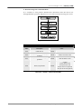
Table of Contents
1. Introduction................................................................. 11
1.1
Scope .............................................................................................................. 11
1.2.
Overview....................................................................................................... 12
1.3.
JPEG Encoder/Decoder............................................................................... 13
1.3.1. JPEG Encoding................................................................................... 13
1.3.2. JPEG Decoding .................................................................................. 13
1.3.3. Image Scaling and Effects................................................................. 13
1.4.
Embedded Memory..................................................................................... 14
1.5.
OSD................................................................................................................ 15
1.6.
Host CPU Interface...................................................................................... 15
1.7.
LCD Controller & CCIR 601/656 Interface.............................................. 15
1.8.
CMOS/CCD Image Sensor Interface ....................................................... 16
1.9.
USB1.1 Device Controller .......................................................................... 16
1.10. SD Card Controller ..................................................................................... 16
1.11. NAND Flash Controller (CL765N Only)................................................. 16
2. Features ........................................................................17
2.1.
Host Interface ............................................................................................... 17
2.2.
Memory ......................................................................................................... 17
2.3.
LCD Support ................................................................................................ 17
2.4.
Sensor Support............................................................................................. 17
2.5.
Display Support........................................................................................... 18
2.6.
Image Effect.................................................................................................. 18
2.7.
Still JPEG Support ...................................................................................... 18
2.8.
MJPEG Support (Movie Camera) ............................................................. 19
2.9.
USB1.1 Device Controller .......................................................................... 19
2.10. TV Encoder Interface .................................................................................. 19
2.11. SD Card Controller ..................................................................................... 19
2.12. NAND Flash Controller (CL765N Only)................................................. 19
2.13. Clock and Power.......................................................................................... 20
2.14. Additional Features..................................................................................... 20
3. Pin Description ............................................................21
3.1.
Pin Diagram.................................................................................................. 21
3.2.
Pin Description ............................................................................................ 22
4. Functional Descriptions .......................................... 28
CORE LOGIC Proprietary and Confidential 3
CL765 │ Camera Application Processor
Datasheet │ Doc. #: CLQP-DS-743
4.1.
Block Diagram ............................................................................................. 28
4.2.
Host Interface ............................................................................................... 30
4.2.1. LCD Access Port ................................................................................. 31
4.2.2. Bypass Mode ....................................................................................... 32
4.2.3. Register Read_n/Write_n Port........................................................... 33
4.3.
Clock Unit..................................................................................................... 34
4.3.1. Frequency of System Clocks ............................................................. 35
4.3.2. Clock Output Control ........................................................................ 38
4.4.
Operation Mode Register........................................................................... 39
4.5.
Preview.......................................................................................................... 41
4.5.1. Preview Setup ..................................................................................... 41
4.5.2. Preview Rotation ................................................................................ 43
4.5.3. Preview Frame Skip ........................................................................... 44
4.6.
JPEG Encoding............................................................................................. 45
4.6.1. Still JPEG Encoding............................................................................ 45
4.6.2. JPEG Quality ....................................................................................... 46
4.6.3. MJPEG Encoding ................................................................................ 47
4.6.4. OSD Encoding..................................................................................... 47
4.7.
JPEG Decoding ............................................................................................ 48
4.7.1. Still JPEG Decoding............................................................................ 48
4.7.2. MJPEG Decoding................................................................................ 48
4.8.
SRAM Buffer Setup .................................................................................... 49
4.9.
SRAM Read .................................................................................................. 50
4.10. SRAM Write ................................................................................................. 50
4.11. PIP (Picture in Picture) ............................................................................... 51
4.12. Flow Control................................................................................................. 53
4.12.1. Detailed Description on Flow Control Architecture.................... 53
4.12.2. Modem CPU Requirement.............................................................. 55
4.12.3. Flowchart & Pseudo Code............................................................... 56
4.13. Display Unit ................................................................................................. 60
4.13.1. Data Format of OSD Image ............................................................. 62
4.13.2. 80-Type LCD Interface ..................................................................... 66
4.13.3. RGB-Type LCD Interface ................................................................. 75
4.13.4. TV Encoder Interface ....................................................................... 78
4.13.5. Multiplexing the Visual Device Interfaces .................................... 80
4.14. Sensor Interface ........................................................................................... 82
4.15. Interrupt Setup ............................................................................................ 88
4.15.1. Interrupt Mode Setup ...................................................................... 88
4.15.2. Type of Interrupt............................................................................... 89
4
Issue Date: 2004/11/05 │ CONFIDENTIAL
www.corelogic.co.kr │
4.15.3. Edge Interrupt................................................................................... 90
4.15.4. Level Interrupt .................................................................................. 91
4.15.5. Status Register................................................................................... 91
4.16. GPIO Setup .................................................................................................. 92
4.17. Image Effect.................................................................................................. 93
4.18. Data Format .................................................................................................. 96
4.19. NAND Flash I/F ..........................................................................................100
4.19.1. Overview ..........................................................................................100
4.19.2. Features.............................................................................................100
4.19.3. Operation Scheme ...........................................................................100
4.19.4. Modem CPU I/F...............................................................................101
4.19.5. DMA Controller I/F .........................................................................101
4.19.6. NAND Flash Memory I/F...............................................................101
4.19.7. ECC (Error Correction Code).........................................................102
4.19.8. Flow Control ....................................................................................102
4.19.9. I/O Timing ........................................................................................112
4.20. DMA Controller & SD Card I/F...............................................................115
4.20.1. Block Diagram..................................................................................115
4.20.2. DMA Controller...............................................................................116
4.20.3. SD I/F.................................................................................................116
4.20.4. SD Operations ..................................................................................117
5. Electrical Characteristics .................................. 123
5.1.
DC Characteristics......................................................................................123
5.2.
AC Characteristics ......................................................................................124
5.2.1. Absolute Maximum Ratings (VSS=0V)...........................................124
5.2.2. Recommended Operating Condition..............................................124
5.2.3. Power Consumption .........................................................................124
6. Package Reference ................................................. 125
CORE LOGIC Proprietary and Confidential 5
CL765 │ Camera Application Processor
Datasheet │ Doc. #: CLQP-DS-743
List of Tables
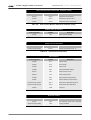
Table 4-1.
Usage of LCD Access Port
(Connecting both A0 and ADS Situation).............................................. 31
6
Table 4-2.
Usage of LCD Access Port (Not Connecting A0 and ADS) ................. 31
Table 4-3.
Register Read/Write .................................................................................. 33
Table 4-4.
Examples of Preview Rotation ................................................................ 44
Table 4-5.
Examples of Preview Rotation ................................................................ 55
Table 4-6.
Alpha Expansion Table ............................................................................ 63
Table 4-7.
LCD Command/Parameter Set Timing Table........................................ 67
Table 4-8.
LCD Type 1 Setup ..................................................................................... 69
Table 4-9.
LCD Type 2 Setup ..................................................................................... 69
Table 4-10.
LCD Window Setup.................................................................................. 69
Table 4-11.
LCD GRAM Setup .................................................................................... 70
Table 4-12.
LCD Window/GRAM Setup.................................................................... 70
Table 4-13.
ADS Polarity .............................................................................................. 70
Table 4-14.
Example of LCD Setup............................................................................. 71
Table 4-15.
LCD Type 1 ................................................................................................ 72
Table 4-16.
LCD Type 2 ................................................................................................ 72
Table 4-17.
0xB5 Setup.................................................................................................. 72
Table 4-18.
0xB6 Setup.................................................................................................. 73
Table 4-19.
0xB7 Setup.................................................................................................. 73
Table 4-20.
0xC0-0xCF Setup....................................................................................... 73
Table 4-21.
0xD0-0xD9 Setup....................................................................................... 73
Table 4-22.
Digital Interface Specification for TV Standards .................................. 79
Table 4-23.
Pin Mapping for Visual Device Interfaces............................................. 81
Table 4-24.
Interrupt Mode.......................................................................................... 88
Table 4-25.
Interrupt Mask Mode ............................................................................... 88
Table 4-26.
Interrupt Status Register 1 ....................................................................... 89
Table 4-27.
Interrupt Status Register 0xe8 ................................................................. 90
Table 4-28.
GPIO Setup Register................................................................................. 92
Table 4-29.
Start of Frame Markers, Non-differential, Huffman Coding.............. 97
Table 4-30.
Start of Frame Markers, Differential, Huffman Coding ...................... 97
Table 4-31.
Start of Frame Markers, Non-differential, Arithmetic Coding ........... 97
Table 4-32.
Start of Frame Markers, Differential, Arithmetic Coding.................... 98
Table 4-33.
Huffman Table Specification ................................................................... 98
Table 4-34.
Restart Interval Termination.................................................................... 98
Issue Date: 2004/11/05 │ CONFIDENTIAL
www.corelogic.co.kr │
Table 4-35.
Other Markers ........................................................................................... 98
Table 4-36.
Reserved Markers ..................................................................................... 98
Table 4-37.
Prepare Register Setting before Operation .......................................... 102
Table 4-38.
Read ID – CPU Command Mode.......................................................... 103
Table 4-39.
Page Program – CPU Command Mode ............................................... 105
Table 4-40.
Page Program – DMA Command Mode.............................................. 106
Table 4-41.
Page Read – CPU Command Mode...................................................... 108
Table 4-42.
Page Read – DMA Command Mode .................................................... 108
Table 4-44.
Block Erasure – DMA Command Mode .............................................. 110
Table 4-45.
Copy-Back - CPU Command Mode ..................................................... 111
CORE LOGIC Proprietary and Confidential 7
CL765 │ Camera Application Processor
Datasheet │ Doc. #: CLQP-DS-743
List of Figures
Figure 4-1.
CL765 System Block Diagram ............................................................... 28
Figure 4-2.
Modem CPU Interface............................................................................ 30
Figure 4-3.
Bypass Mode ........................................................................................... 32
Figure 4-4.
Camera Mode: Register Write ............................................................... 33
Figure 4-5.
Camera Mode: Register Read................................................................ 33
Figure 4-6.
Block Diagram of Clock Unit ................................................................ 34
Figure 4-7.
System Clock Generation from PLLCLK............................................. 36
Figure 4-8.
Preview Area Setup (VGA).................................................................... 41
Figure 4-9.
Example of SRAM Buffer Setup............................................................ 50
Figure 4-10.
Bit Configuration of PIP Pixel Data...................................................... 51
Figure 4-11.
Flow Control............................................................................................ 54
Figure 4-12.
Encoding Flowchart................................................................................ 56
Figure 4-13.
Decoding Flowchart ............................................................................... 58
Figure 4-14.
Data-flow of Display Unit...................................................................... 60
Figure 4-15.
Example of Alpha-blending .................................................................. 61
Figure 4-16.
The Bit Expansion for 8Bit-index Color ............................................... 62
Figure 4-17.
The Bit Expansion for 444-αRGB Color ............................................... 63
Figure 4-18.
The Bit Expansion for 565-RGB Color.................................................. 64
Figure 4-19.
Chroma-keying ....................................................................................... 65
Figure 4-20.
The Generic Interconnection to LCD Modules ................................... 66
Figure 4-21.
Camera Mode and LCD_Display ......................................................... 67
Figure 4-22.
LCD Command/Parameter Set Timing................................................ 67
Figure 4-23.
LCD Gram Data Write Timing .............................................................. 68
Figure 4-24.
LCD Lock during Camera Mode .......................................................... 74
Figure 4-25.
The Generic Interconnection between the CL765
and RGB-Type LCD Module ................................................................. 75
8
Figure 4-26.
The Video Signal Timing Diagram for RGB-Type LCD Module...... 78
Figure 4-27.
The Generic Interconnection between the CL765 and TV Encoder . 78
Figure 4-28.
Timing Diagram for CCIR601/656 Interface........................................ 80
Figure 4-29.
Sensor RESET and IIC Write Time........................................................ 82
Figure 4-30.
IIC Write ................................................................................................... 82
Figure 4-31.
IIC Read.................................................................................................... 83
Figure 4-32.
Sensor Data Sampling ............................................................................ 84
Figure 4-33.
Sensor Power Supply Sequence ............................................................ 85
Figure 4-34.
IIC Operation Hold Time....................................................................... 86
Issue Date: 2004/11/05 │ CONFIDENTIAL
www.corelogic.co.kr │
Figure 4-35.
Edge Interrupt Pin Status ...................................................................... 90
Figure 4-36.
Level 1 Interrupt Pin Status................................................................... 91
Figure 4-37.
Read ID – Flowchart ............................................................................. 103
Figure 4-38.
Page Program – Flowchart................................................................... 104
Figure 4-39.
Page Read – Flowchart ......................................................................... 107
Figure 4-40.
Block Erasure – Flowchart ................................................................... 109
Figure 4-41.
Copy-Back – Flowchart ........................................................................ 110
Figure 4-42.
Host Interface Timing – Write ............................................................. 112
Figure 4-43.
Host Interface Timing – Read.............................................................. 112
Figure 4-44.
DMA Controller Interface Timing – NAND Flash Memory Read . 113
Figure 4-45.
DMA Controller Interface Timing – NAND Flash Memory Write 113
Figure 4-46.
NAND Flash Memory Timing (ex. TACLS=1, TWRPH0=2,
TWRPH1=1) ........................................................................................... 114
Figure 4-47.
DMA Controller & SD Card I/F Block Diagram ............................... 115
Figure 4-48.
FAT Table for DAM............................................................................... 116
Figure 4-49.
SD Initialization Process ...................................................................... 117
Figure 4-50.
SD Polling Mode Read without FAT .................................................. 118
Figure 4-51.
SD DMA Mode Read without FAT ..................................................... 119
Figure 4-52.
SD Polling Mode Write without FAT.................................................. 120
Figure 4-53.
SD DMA Mode Write without FAT .................................................... 121
Figure 4-54.
SD DMA Mode Read with FAT........................................................... 122
Figure 4-55. SD DMA Mode Write with FAT ..........................................................122
CORE LOGIC Proprietary and Confidential 9
CL765 │ Camera Application Processor
Datasheet │ Doc. #: CLQP-DS-743
THIS PAGE LEFT BLANK
10 Issue Date: 2004/11/05 │ CONFIDENTIAL
www.corelogic.co.kr │
1. INTRODUCTION
1.1. SCOPE
In this document, hardware functional specification for CL765 – CORE LOGIC’s
Mobile Camera Application Processor – is described. The main scope of this
document includes internal hardware functionality, interfaces to external devices,
AC/DC characteristics, register descriptions and package information. This
document is written and organized for mainly two groups of engineers: system
designer and software programmer. System designers refer to this document for
designing system level interconnections between the CL765 and other system
components, while software programmers refer to this document to understand
the detailed functionalities and internal registers of the CL765.
CORE LOGIC Proprietary and Confidential 11
CL765 │ Camera Application Processor
Datasheet │ Doc. #: CLQP-DS-743
1.2. OVERVIEW
CORE LOGIC’s CL765 is an easy, convenient and high-performance camera
application processor (CAP) designed to meet the needs of mobile platformrelated industry, manufacturers and developers: least effort and cost in
developing their system, as well as a lot of outstanding features and
functionalities.
The CL765 contains various highly-advanced functions such as fully-hardwired
JPEG codec, image scalar for Digital Zoom Function, MJPEG codec, high-speed
Image data processing, OSD and so on. For the system level integration, the
CL765 provides various off-chip interfaces including CMOS/CCD camera sensor
interface, LCD interface, SD card interface and CCIR601/656 interface for external
TV encoder interface.
The main design objective of the CL765 is providing system-level low cost and
low power solution with plenty sets of functions required by most Mobile Digital
systems: The advanced image processing functions of the CL765 are implemented
with its 256K bytes of embedded SRAM. This eliminates the use of external
memories and hence system-level low cost and low power consumption will be
achieved. Additionally, seamless interconnection with external devices also
reduces system-level cost and the size of Mobile system by eliminating the use of
external glue-logics.
The key functions and external device controllers/interfaces are as follows:
JPEG and MJPEG encoder/decoder
256K bytes embedded memory
OSD
Host interface
LCD controller
CMOS/CCD image sensor interface
USB1.1 device controller
SD card controller
NAND flash controller
12 Issue Date: 2004/11/05 │ CONFIDENTIAL
www.corelogic.co.kr │
1.3. JPEG ENCODER/DECODER
The CL765 has a fully-hardwired JPEG codec. It encodes an image incoming from
CMOS/CCD image sensor, and decodes a JPEG stream sent from Host CPU.
During the encoding/decoding, various image processing like scaling, image
effects are pre/post-processed by using dedicated hardware blocks.
1.3.1. JPEG Encoding
The CL765 encodes an image either from camera sensor (this function is called as
JPEG capture) or stored in frame buffer into JPEG stream (this function is called as
BMP2JPEG). The data format at input stage of JPEG encoder is 4:2:2-YCbCr. The
format of data from camera sensor is 4:2:2-YCbCr, and hence the image from
camera can be encoded without data format conversion. For images in frame
buffer, not only the video image but also OSD image, they are mixed into one
image in RGB color space, converted to 4:2:2-YCbCr format and sent to JPEG
encoder. Before JPEG encoding, the original image is resized and translated
through dedicated hardware scaler and image effecter, respectively.
The encoded JPEG stream is stored into internal memory and transmitted to Host
CPU. The CL765 uses so-called flow-control scheme to transmit encoded stream
to Host CPU. In short, the scheme permits Host CPU to read on-making JPEG
stream simultaneously with JPEG encoding. The scheme eliminates image size
limitation in JPEG encoding, and hence Host CPU can capture larger size (up to
3M pixel) image than the CL765’s internal memory.
1.3.2. JPEG Decoding
The CL765 decodes a JPEG stream from Host CPU, and stores the result 4:2:2YCbCr image into its Video Buffer. The stored image can be displayed on output
visual devices (LCD or TV) or can be transmitted to Host CPU. Before storing the
BMP into Video Buffer, the CL765 (optionally) resizes and translates the decoded
image by using scaler and image effecter.
Like the encoding operation, decoding operation also uses the flow-control
scheme. In this case, JPEG decoder decodes JPEG stream while Host CPU writes
the JPEG stream into the CL765’s internal memory.
1.3.3. Image Scaling and Effects
As described above, the CL765 has a dedicated hardware scaler and an image
effecter. The scaler is used for image scaling and digital zoom. The zoon-in and
zoom-out can be supported up and down to 4X and 1/16X, respectively. The scaler
uses multi-tap image filter to reduce artifacts caused by scaling, and hence keeps
high quality of resulting image. The image effecter consists of various image
profiler and filters such as edge detector, hue compensator, gamma corrector, etc.
CORE LOGIC Proprietary and Confidential 13
CL765 │ Camera Application Processor
Datasheet │ Doc. #: CLQP-DS-743
1.4. EMBEDDED MEMORY
The CL765 embeds 256K bytes of internal SRAM that is accessible by Host CPU
(The CL765 embeds Strip Buffer also, but the Strip Buffer is not visible and
accessible for Host CPU. It is internally used only). The internal memory is used
mainly for JPEG encoding/decoding and buffer for OSD image. Host CPU can
access the whole space of the memory through Host interface protocol (refer to
4.2). The memory is conceptually partitioned into several dedicated spaces and
used. The partitioned spaces are as follows:
FIFO for Flow Control: flow-control scheme uses a part of internal memory
for transmitting data between Host CPU and the CL765. The internal memory
is used as a FIFO which is managed as a loop-buffer, i.e., for when
read/writer pointers reach to top of the FIFO, they are automatically set back
to bottom position. The size of FIFO buffer is programmable.
Video Buffer: the Video Buffer is the memory area assigned to video image
to be sent out through external visual devices interface. The size of Video
Buffer is programmable and generally same to the size of external visual
device, i.e., for LCD display, video buffer size is the same to the size of LCD
panel. The data format of image in Video Buffer is 4:2:2-YCbCr. Host CPU can
read YCbCr formatted image data from Video Buffer directly.
BMP Buffer: after JPEG2BMP Operation, additional to video image (that is
store into Video buffer after scaling), the decoded original (that means nonscaled) image is also stored into internal memory that is called BMP Buffer.
Note) Refer to Bit[13] of JPEG2BMP in 4.4 Operation Mode Register
OSD Buffers: the CL765 provides two separated OSD images, OSD1 and
OSD2. The format of OSD is one of three types: 8bit-indexed, 4444-αRGB and
565-RGB.
Thumbnail Buffer: the RGB Thumbnail Buffer contains image for currently
being encoded image. The data format of thumbnail is 4:2:2-YCbCr. The size
of thumbnail is programmable (maximum size is 160 x 120).
14 Issue Date: 2004/11/05 │ CONFIDENTIAL
www.corelogic.co.kr │
1.5. OSD
The CL765 supports OSD. OSD is the function to compound Camera image and
Background BMP image and dispkay that on LCD. OSD has Overwrite function
and Overlay function and Chroma-Key is used to perform the functions. ChromaKey is a special key used for the area where OSD BMP image and Camera image
are displayed. It is used to distinguish Camera image from OSD BMP image. The
OSD is a collection of functions that composes video image from camera and
graphical bitmap image (OSD image) mainly for displaying menus, and then
displays on external visual devices. The CL765 supports two separated OSD
images and the bitmap formats for OSD image are 8bit–indexed, 4444-αRGB and
565-RGB. The 8bit-index format is 8bpp while 4444-αRGB and 565-RGB are 16bpp.
The OSD functions that provided by the CL765 are alpha blending and chromakeying. The alpha blending is a function that blends background (generally video
image) and foreground (generally OSD image) according to given blend ratio,
while the chroma-keying is a multiplexing function.
1.6. HOST CPU INTERFACE
The CL765 provides 18-bit wide bus for Host CPU interface. There are two main
usages of Host CPU interface, for register/memory accesses or for LCD accesses.
In normal operation mode, i.e., the CL765 is activated, the Host CPU interface is
used for accessing the CL765’s internal registers and memories. In the mode, only
lower 16-bit of data bus is used. In Bypass mode, i.e., the CL765 is sleep and the
Host interface is connected to the CL765’s LCD interface, Host CPU can directly
read and write the LCD module. In the mode, 18-bit data bus is used to access
registers and GRAM of LCD module.
1.7. LCD CONTROLLER & CCIR 601/656 INTERFACE
The CL765 supports various LCD modules mainly for 80-Type LCD modules and
RGB-Type LCD modules.
For 80-Type LCD modules, the data bus between the CL765 and LCD module is
configured up to 18 bits (actually one of 8-bit, 9-bit, 12-bit, 16-bit and 18-bit). For
the LCD, two LCD modules can be connected to the CL765, i.e., main LCD and
sub LCD.
For RGB-Type LCD modules, the data bus width is one of 6-bit of 18-bit. For the
modules, the CL765 provides and generates pixel-clock, horizontal-/vertical-sync
and video data enable with data bus. The LCD sync timing is programmable, so
various sized LCD modules can be controlled by the CL765.
Two-LCD mode, main and sub LCD’s, only one LCD can be activated at a time.
For two-LCD mode, different types of LCD can also be used. For example, a RGBType for main LCD and an 80-Type for sub LCD are applicable.
CORE LOGIC Proprietary and Confidential 15
CL765 │ Camera Application Processor
Datasheet │ Doc. #: CLQP-DS-743
Additional to LCD interface, the CL765 provides CCIR601/656 interface for
external TV encoder. The visual data output through the interface is compliant to
CCIR601 or CCIR656 specification for either NTSC encoders or PAL/SECAM
encoders.
1.8. CMOS/CCD IMAGE SENSOR INTERFACE
The CL765 supports various CMOS/CCD image sensor interface. The general
interconnection with a sensor is a combination of CCIR601/656 interface for
transferring image data and IIC interface for setting sensor’s internal registers.
1.9. USB1.1 DEVICE CONTROLLER
There is an USB1.1 device controller in the CL765. The supported transfer types
provided by the CL765 are USB1.1 control transfer and bulk type transfer.
1.10. SD CARD CONTROLLER
The CL765 contains a SD card (SDC) controller to support the storage for large
size multimedia data. The SD card controller provides the SD Memory Card
Physical Layer Version1.0 compatible interface in 4-bit or 1-bit transfer modes. It
supports command setting, status report, block data read/write and error
detection during transfer.
1.11. NAND FLASH CONTROLLER (CL765N ONLY)
The CL765N contains NAND flash memory controller. The NAND flash controller
supports various size of NAND flash with 8-bit or 16-bit data width. The
hardware functions which are provided by the controller include command
setting, status report, block data read/write and CRC code generation/comparison.
16 Issue Date: 2004/11/05 │ CONFIDENTIAL
www.corelogic.co.kr │
2. FEATURES
2.1. HOST INTERFACE
16bit 80-Type Parallel Host interface
Indirect Addressing: Uses 2-bit Address bus.
8/16/18 bit Parallel LCD bypass mode supported
2.2. MEMORY
Embedded 256K bytes of SRAM
FIFO for flow-control, Video Buffer, OSD Buffer, BMP Buffer, Thumbnail
Buffer and Strip Buffer Embedded
2.3. LCD SUPPORT
Supports LCD bypass mode
supports 80-Type and RGB-Type LCD modules
Supports 4 gray, 16 gray, 8/12/16/18 bit Color STN/UFB/TFT LCD modules
Includes Video Buffer for high speed GRAM write
Supports high resolution LCD modules (up to 176 x 220)
Supports programmable Display Window Size
Supports Sub-LCD at the same features as Main LCD
2.4. SENSOR SUPPORT
CCIR601, CCIR656, YCbCr 4:2:2 Compliant with 8-bit Interface
Internal Clock Divider 1/1, 1/2, 1/4 for Sensor Clock Output
Supports Standard IIC BUS
Programmable Clock Polarity
Up to 3M pixel resolution(2048 x 1560)
CORE LOGIC Proprietary and Confidential 17
CL765 │ Camera Application Processor
Datasheet │ Doc. #: CLQP-DS-743
2.5. DISPLAY SUPPORT
Supports Frame Rate Up to 30 fps (depends on Sensor Frame rate)
Supports Fully Hardwired Image Scalar (up to 4X Zoom – horizontally 2X
and vertically 2X - in comparing to the original image size)
Supports Real Zoom
Supports Real-time Hardwired Display Rotation (90°, 180°,270°,mirror, flip)
Supports OSD modes (i.e. alpha-blending and chroma-keying)
Supports YCbCr 4:2:2 format for video image
Supports 8bit-index (8bpp), 4444-αRGB (16bpp), 565-RGB (16bpp) format for
OSD images
2.6. IMAGE EFFECT
Warm, Cool, Fog, Antique, Sepia, Tan, Moonlight, Negation, Embossing
Summation with Color-Tone
2.7. STILL JPEG SUPPORT
Fully Hardwired DCT, RLE, and Huffman Encoding
Encodes ITU-T T.81 Compliant Baseline Sequential JPEG Scan Image
Encodes Up to 2048x1536 Size with Free Size Support
JPEG Still Capture with Image Effect
JPEG Still Capture with OSD
Via-continuous Shooting JPEG Still Capture
Supports JPEG Decoding for Various JPEG Image Formats (4:4:4, 4:2:2, 4:2:0,
4:1:1)
Supports Still Zoom
Supports 32-Byte JPEG Application Maker for Vendor Information
18 Issue Date: 2004/11/05 │ CONFIDENTIAL
www.corelogic.co.kr │
2.8. MJPEG SUPPORT (MOVIE CAMERA)
Fully Hardwired DCT, RLE, and Huffman Encoding
Hardwired MJPEG CODEC (To use Flow Control Scheme, S/W Support is
required)
Supports the Same Features as those for JPEG Still Image Capture
Supports Real-Time Clock-Based Time Stamp for Audio Support
No time limitation on recording (To use Flow Control Scheme, S/W Support
is required)
Supports Frame Skip for Expansion of Recoding Time
Supports MJPEG Decoding (To use Flow Control Scheme, S/W Support is
required)
2.9. USB1.1 DEVICE CONTROLLER
Supports USB1.1 compliant control and burst transfer
On-chip USB1.1 transceiver
2.10. TV ENCODER INTERFACE
Supports CCIR601 or CCIR656 interface for external TV encoder
Provides 8-bit data bus with 27MHz clock and sync signals
Supports NTSC, PAL, SECAM standards
2.11. SD CARD CONTROLLER
SD Memory Card Physical Layer Version1.0 compatible
Supports 4-bit or 1-bit transfer mode
Hardwired CRC error detector
2.12. NAND FLASH CONTROLLER (CL765N ONLY)
Supports various size of NAND flash memory
8-bit/16-bit data bus width
Hardware CRC generation/comparison
CORE LOGIC Proprietary and Confidential 19
CL765 │ Camera Application Processor
Datasheet │ Doc. #: CLQP-DS-743
2.13. CLOCK AND POWER
Full CMOS Technology
Equipped with PLL of which output frequency is programmable
Supports 5MHz to 20MHz for input clock
Supports maximum 40MHz of internal main clock (32MHz is recommended)
Typically consumes under 100uA during Sleep Mode
Supports Preview & Capture Mode, under 28mA Consumption @ 20MHz
(internal main clock)
2.14. ADDITIONAL FEATURES
Supports General Purpose I/Os
Supports Edge/Level Programmable Interrupt Source
100 pin BGA Package (8.0 x 8.0 mm)
20 Issue Date: 2004/11/05 │ CONFIDENTIAL
www.corelogic.co.kr │
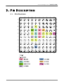
3. PIN DESCRIPTION
3.1. PIN DIAGRAM
CORE LOGIC Proprietary and Confidential 21
Datasheet │ Doc. #: CLQP-DS-743
CL765 │ Camera Application Processor
3.2. PIN DESCRIPTION
Modem CPU Interface (29 pins)
Pin
Pin Name
I/O Type
NO.
Drive
Interface
(mA)
Group
Description
K10
M_SA0
Input
Modem CPU
Modem CPU Address Bus 0
K9
M_SA1
Input
Modem CPU
Modem CPU Address Bus 1
J10
M_SD0
Input/Output
4
Modem CPU
Modem CPU Data Bus 0
J9
M_SD1
Input/Output
4
Modem CPU
Modem CPU Data Bus 1
J8
M_SD2
Input/Output
4
Modem CPU
Modem CPU Data Bus 2
J7
M_SD3
Input/Output
4
Modem CPU
Modem CPU Data Bus 3
J6
M_SD4
Input/Output
4
Modem CPU
Modem CPU Data Bus 4
H10
M_SD5
Input/Output
4
Modem CPU
Modem CPU Data Bus 5
H9
M_SD6
Input/Output
4
Modem CPU
Modem CPU Data Bus 6
H8
M_SD7
Input/Output
4
Modem CPU
Modem CPU Data Bus 7
H7
M_SD8
Input/Output
4
Modem CPU
Modem CPU Data Bus 8
H6
M_SD9
Input/Output
4
Modem CPU
Modem CPU Data Bus 9
G10
M_SD10
Input/Output
4
Modem CPU
Modem CPU Data Bus 10
G9
M_SD11
Input/Output
4
Modem CPU
Modem CPU Data Bus 11
G8
M_SD12
Input/Output
4
Modem CPU
Modem CPU Data Bus 12
G7
M_SD13
Input/Output
4
Modem CPU
Modem CPU Data Bus 13
G6
M_SD14
Input/Output
4
Modem CPU
Modem CPU Data Bus 14
F10
M_SD15
Input/Output
4
Modem CPU
Modem CPU Data Bus 15
Modem CPU Data Bus 16
F9
M_SD16
Input
Modem CPU
Connect this pin to GRN when
Modem CPU 18bit Interface is not
used.
Modem CPU Data Bus 17
F8
M_SD17
Input
Modem CPU
Connect this pin to GRN when
Modem CPU 18bit Interface is not
used.
Camera chip / Main LCD select
D8
M_CS_N
Input
Modem CPU
-
When HOLD is HIGH, Main LCD
chip select
-
When HOLD is LOW, Camera
chip select
-
HOLD is set by Register 0xa1
Bit[0]
22 Issue Date: 2004/11/05 │ CONFIDENTIAL
www.corelogic.co.kr │
Pin
Pin Name
I/O Type
NO.
Drive
Interface
(mA)
Group
Description
Sub-LCD chip select.
In order to have modem CPU
control Sub-LCD directly, connect
K7
this pin to
MS_CS_N
-
When HOLD is HIGH, Sub-LCD
chip select
-
When HOLD is LOW, Camera
chip select
B9
M_WR_N
Input
Modem CPU
Modem CPU Write Enable
C9
M_RD_N
Input
Modem CPU
Modem CPU Read Enable
K8
M_ADS
Input
Modem CPU
Address/Data Selection
B10
M_INTR
Output
Modem CPU
Camera IC’s Interrupt
D9
M_RESET_N
Input
Modem CPU
RESET (active low)
D10
XIN
Input
Crystal(OSC)
Clock Input
C10
XOUT
Output
Crystal
4
Clock Output
CORE LOGIC Proprietary and Confidential 23
Datasheet │ Doc. #: CLQP-DS-743
CL765 │ Camera Application Processor
Sensor Interface (16 pins)
Pin
Pin Name
I/O Type
NO
Drive
Interface
(mA)
Group
Description
A4
C_D0
Input
Sensor
Sensor Data Bus 0
A5
C_D1
Input
Sensor
Sensor Data Bus 1
B4
C_D2
Input
Sensor
Sensor Data Bus 2
B5
C_D3
Input
Sensor
Sensor Data Bus 3
B6
C_D4
Input
Sensor
Sensor Data Bus 4
C3
C_D5
Input
Sensor
Sensor Data Bus 5
C4
C_D6
Input
Sensor
Sensor Data Bus 6
C6
C_D7
Input
Sensor
Sensor Data Bus 7
B3
C_HS
Input
Sensor
HSYNC/HREF Input
A3
C_VS
Input
Sensor
VSYNC Input
A2
C_RST
Output
Sensor
Sensor RESET
A1
C_PCLK
Input
Sensor
Input Data sampling clock
A6
C_MCLK
Output
4
Sensor
Sensor clock
B2
C_SDA
Input/Output
8
Sensor
IIC Bus Data line
B1
C_SCK
Output
8
Sensor
IIC Bus Clock line
A7
C_PWDN
Output
4
Sensor
Sensor power control pin. This pin
4
controls the circuit that provides
power to sensor and is under
Camera
LOW.
24 Issue Date: 2004/11/05 │ CONFIDENTIAL
operation
mode
when
www.corelogic.co.kr │
LCD Interface (23 pins)
Pin
Pin Name
I/O Type
NO.
Drive
Interface
(mA)
Group
Description
C2
L_DA0
Input/Output
8
LCD
LCD Address/Data Bus 0
C1
L_DA1
Input/Output
8
LCD
LCD Address/Data Bus 1
D1
L_DA2
Input/Output
8
LCD
LCD Address/Data Bus 2
D2
L_DA3
Input/Output
8
LCD
LCD Address/Data Bus 3
D3
L_DA4
Input/Output
8
LCD
LCD Address/Data Bus 4
E1
L_DA5
Input/Output
8
LCD
LCD Address/Data Bus 5
E2
L_DA6
Input/Output
8
LCD
LCD Address/Data Bus 6
E3
L_DA7
Input/Output
8
LCD
LCD Address/Data Bus 7
F1
L_DA8
Input/Output
8
LCD
LCD Address/Data Bus 8
F2
L_DA9
Input/Output
8
LCD
LCD Address/Data Bus 9
F3
L_DA10
Input/Output
8
LCD
LCD Address/Data Bus 10
G3
L_DA11
Input/Output
8
LCD
LCD Address/Data Bus 11
G2
L_DA12
Input/Output
8
LCD
LCD Address/Data Bus 12
G1
L_DA13
Input/Output
8
LCD
LCD Address/Data Bus 13
H1
L_DA14
Input/Output
8
LCD
LCD Address/Data Bus 14
H2
L_DA15
Input/Output
8
LCD
LCD Address/Data Bus 15
H3
L_DA16
Input/Output
8
LCD
LCD Address/Data Bus 16
H4
L_DA17
Input/Output
8
LCD
LCD Address/Data Bus 17
K1
L_CS_N
Output
8
LCD
LCD chip select
H5
LS_CS_N
Output
8
LCD
Sub-LCD chip select
J2
L_WR_N
Output
8
LCD
Write enable
J3
L_RD_N
Output
8
LCD
Read enable
K2
L_ADS
Output
8
LCD
Address/Data selection
CORE LOGIC Proprietary and Confidential 25
Datasheet │ Doc. #: CLQP-DS-743
CL765 │ Camera Application Processor
Other pins (13 pins)
Pin
Pin Name
I/O Type
NO.
Drive
Interface
(mA)
Group
Description
Pin to control the action of Strobe
A10
STROBE
Output
4
K5
USB_DP
Input/Output
USB
USB Differential Data Bus
K6
USB_DM
Input/Output
USB
USB Differential Data Bus
light.
-
GPIO
When not using these pins,
connect them to GND.
B7
GPIO_0
(SD_CLK)
Input/Output
4
GPIO / SD
CARD
-
SD CARD Interface
This pin is used SD CARD
CLOCK and in this case, it works
as an output pin.
-
GPIO
When not using these pins,
C7
GPIO_1
(SD_CMD)
Input/Output
connect them to GND.
4
-
SD CARD Interface
Assigned to SD CARD Command
line.
-
GPIO
When not using these pins,
A8
GPIO_2
(SD_D0)
Input/Output
4
GPIO / SD
CARD
connect them to GND.
-
SD CARD Interface
Assigned to SD CARD Data 0.
-
GPIO
When not using these pins,
B8
GPIO_3
(SD_D1)
Input/Output
4
GPIO / SD
CARD
connect them to GND.
-
SD CARD Interface
Assigned to SD CARD Data 1.
-
GPIO
When not using these pins,
C8
GPIO_4
(SD_D2)
Input/Output
4
GPIO / SD
CARD
connect them to GND.
-
SD CARD Interface
Assigned to SD CARD Data 2.
-
GPIO
When not using these pins,
A9
GPIO_5
(SD_D3)
Input/Output
4
GPIO / SD
CARD
connect them to GND.
-
SD CARD Interface
Assigned to SD CARD Data 3.
J4
SCAN_EN
Input
Reserved (LOW)
K4
T_MODE0
Input
Reserved (LOW)
K3
GPIO
Input/Output
4
GPIO Pin
When not using these pins,
connect them to GND.
26 Issue Date: 2004/11/05 │ CONFIDENTIAL
www.corelogic.co.kr │
Pin
Pin Name
I/O Type
NO.
Drive
Interface
(mA)
Group
Description
-
GPIO
When not using these pins,
A9
GPIO_5
(SD_D3)
Input/Output
4
GPIO / SD
CARD
connect them to GND.
-
SD CARD Interface
Assigned to SD CARD Data 3.
Power pins (19 pins)
Pin
Pin Name
I/O Type
NO.
Drive
Interface
(mA)
Group
Description
D4
VDDs
Sensor Power
SENSOR VDD pin
D6
VDDi
I/O Power
I/O VDD pin
E6
VDDi
IO Power
I/O VDD pin
F6
VDDi
I/O Power
I/O VDD pin
D5
VDDc
Core Power
Core VDD pin
E5
VDDc
Core Power
Core VDD pin
F5
VDDc
Core Power
Core VDD pin
F4
VDDl
Lcd Power
LCD VDD pin
D7
VDDsd
SD Power
SD Card VDD pin
E10
VDDpll
PLL Power
PLL VDD pin
J5
VDDusb
USB Power
USB VDD pin
C5
Ground
GND pin
E4
Ground
GND pin
E7
Ground
GND pin
E8
Ground
GND pin
E9
Ground
GND pin
F7
Ground
GND pin
G4
Ground
GND pin
G5
Ground
GND pin
CORE LOGIC Proprietary and Confidential 27
CL765 │ Camera Application Processor
Datasheet │ Doc. #: CLQP-DS-743
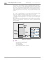
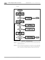
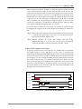
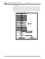
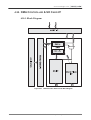
4. FUNCTIONAL DESCRIPTIONS
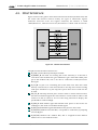
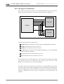
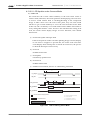
4.1. BLOCK DIAGRAM
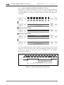
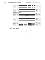
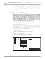
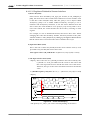
Figure 4-1 shows the overall system diagram of the CL765.
CL765
Video Out
MODEM
CPU
SENSOR
Figure 4-1. CL765 System Block Diagram
The basic function of each hardware block in the figure is as follow:
Frame Buffer: Temporary buffer for video that the CL765 manages.
Modem CPU Interface: Provides interface with Modem CPU
Video scalar: Processes and adjusts size of images that are received from the
sensor or images that are JPEG-decoded, as desired.
CCD/CIS Interface & Control: Provides interface with CCDs or CMOS-based
sensors.
28 Issue Date: 2004/11/05 │ CONFIDENTIAL
www.corelogic.co.kr │
Strip Buffer: Transforms the line data received from sensor into block data,
or JPEG-decoded block data into line data.
Memory Controller: Controls various accesses to Frame buffer.
JPEG Codec: JPEG encoder/decoder
System Controller: Controls power and the CL765 overall actions.
YCbCr-to-RGB Converter: Transforms YCbCr into RGB, or vice versa.
LCD/OSD Controller: Controls main-LCD and sub-LCD.
CPU Type LCD Interface: Controls and Interface CPU type main-LCD and
sub-LCD.
RGB Type LCD Interface: Controls and Interface RGB type LCD
CCIR 601 / CCIR 656 Interface: Control and Interface TV Out Interface
NAND Flash Interface: NAND Flash Memory Interface Block
SD CARD Interface: SD CARD Interface Block
CORE LOGIC Proprietary and Confidential 29
CL765 │ Camera Application Processor
Datasheet │ Doc. #: CLQP-DS-743
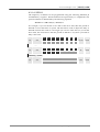
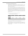
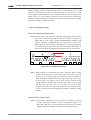
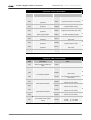
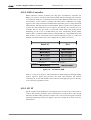
4.2. HOST INTERFACE
Figure 4-2 shows the generic interconnection between the host (modem CPU) and
the CL765. The interface used for mainly two types of interactions, register
read/write and LCD access. For register read/write, the interface is called
“Index/Data Port”, while for LCD access, the interface is called “LCD Access Port”.
M_RESET_N
Figure 4-2. Modem CPU Interface
The pins used in the interconnection are:
M_CLK: CL765’s Main System Input CLOCK
M_RESET_N: Pin used for resetting the CL765. Generally, it is the best to
reset the IC after modem CPU gets stabilized. It gets connected to RES_OUT
pin of the modem CPU, but it can also be connected to POR (Power-OnReset) pin.
M_CS_N: CS pin is for controlling the CL765 main LCD. Since the CL765
directly controls LCD, it is the most efficient to use chip select for the existing
LCD space. Needless to say, the chip select pin of other areas of LCD can also
be used.
MS_CS_N: The chip selection pin is for the CL765 to control sub-LCD. Here,
the sub LCD should support the same interface as main LCD in order for the
CL765 to be able to control it. In case of not using sub-LCD for display, this
pin should be connected High.
M_WR_N: Write Enable signal that Modem CPU passes to the CL765. For
LCD Bypass, this used as LCD Write Enable signal.
M_RD_N: Read Enable signal that Modem CPU passes to the CL765.
M_SD[17:0]: Modem CPU Data Bus, corresponds to LCD Data (L_DA[17:0])
for LCD Bypass.
M_SA[1:0]: Modem CPU Address Bus, 2bit is assigned because Indirect
Address Access is used in the CL765.
30 Issue Date: 2004/11/05 │ CONFIDENTIAL
www.corelogic.co.kr │
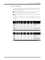
4.2.1. LCD Access Port
LCD Access Port bypasses 1) the CL765’s any bypass mode and 2) LCD lock
status in camera mode for Data (16 bits) and control signals (CS, WR, RD). LCD
access port has Port 0 and Port 1.
Port 0: When using A0 and ADS connections together, it bypasses write of
LCD command and command parameters for most vendors LCD.
Port 1: When using A0 and ADS connections together, it writes LCD GRAM
data.
If A0 and ADS connections are not used together, then both Ports can be used
identically. In this case, ADS pin must be connected to other Address lines except
A1 and A0.
Access
Port
A1
A0
M_CS_N
M_RD_N
M_WR_N
M_ADS
0
0
0
1
0
0
0
1
0
1
0
1
LCD
Access
Port0
LCD
Access
Operation
Write LCD Command or
Parameters.
GRAM data write (Some
Port1
vendor’s LCD only writes
Command parameters.)
Table 4-1. Usage of LCD Access Port (Connecting both A0 and ADS Situation)
Access
Port
A1
A0
M_CS_N
M_RD_N
M_WR_N
M_ADS
0
X
0
1
0
0
0
X
0
1
0
1
LCD
Access
Port0
LCD
Access
Port1
Operation
Write LCD Command or
Parameters.
GRAM data write (Some
vendor’s LCD only writes
Command parameters.)
Table 4-2. Usage of LCD Access Port (Not Connecting A0 and ADS)
CORE LOGIC Proprietary and Confidential 31
CL765 │ Camera Application Processor
Datasheet │ Doc. #: CLQP-DS-743
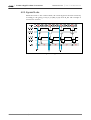
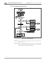
4.2.2. Bypass Mode
When the CL765 is not Camera Mode, the CL765 bypasses the Data selectively
according to the gating of M_CS_N (MS_CS_N) from M_SD. The example of
waveform is as below.
Figure 4-3. Bypass Mode
32 Issue Date: 2004/11/05 │ CONFIDENTIAL
www.corelogic.co.kr │
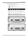
4.2.3. Register Read_n/Write_n Port
The CL765 accesses registers by indirect addressing method. There are two types
for this purpose, Index and Data.
Index Port: Selects Read/Write register.
Data Port: Reads/writes data to the selected register from Index Port.
Port
M_SA
M_CS_N
M_RD_N
M_WR_N
2
0
1
0
2
0
0
1
3
0
1
0
3
0
0
1
Index port
Data port
Operation
Selects Register
Read from currently selected
register.
Write data to selected register
from Index port
Read data to selected register
from Index port
Table 4-3. Register Read/Write
Figure 4-4. Camera Mode: Register Write
Figure 4-5. Camera Mode: Register Read
CORE LOGIC Proprietary and Confidential 33
Datasheet │ Doc. #: CLQP-DS-743
CL765 │ Camera Application Processor
4.3. CLOCK UNIT
The CL765 has on-chip PLL of which output clock (PLLCLK) frequency is up to
200MHz. The Clock Unit uses the PLL output clock as its source clock and has
various system clock dividers. The system clocks used for internal hardware
blocks are as follows;
M1CLK and M2CLK: system main clocks. The M1CLK is used for Host
interface and internal memories, while M2CLK is used for JPEG codec, scaler,
image effecter, etc. By providing separated two main clocks, Host CPU can
turn off non-operating hardware blocks and reduce power consumption. The
frequency of the clocks is 32MHz (recommended).
USBCLK: clock for USB1.1 controller. The frequency for the clock must be
48MHz.
RGBCLK: clock for RGB-Type LCD controller. Host CPU can program the
clock frequency with respect to LCD size.
TVCLK: clock for CCIR601/656 interface unit. The frequency for the clock
must be 27MHz.
SDCLK: clock for SD card controller. The clock is used for line clock of SD
card interface. The frequency of the clock is programmable ranging from
1MHz to 10MHz.
As shown in Figure 4-6, due to single source clock (PLLCLK) for clock dividers,
USBCLK and TVCLK can not be generated at the same time – They need the fixed
clock frequencies, 48MHz for USBCLK and 27MHz for TVCLK, and 432MHz for
input clock is required to generate them by using integer dividers. Therefore, the
CCIR601/656 controller and USB controller can not be activated at the same time.
In addition to generating system clocks, clock unit provides turning-off features
for each system clock for the purpose of reducing power consumption.
SDCLK
Divider
PLLCLK
X_TAL
X_TAL
PLL
MCLK
Divider
M1CLK_CE
M2CLK_CE
USBCLK
Divider
RGBCLK
Divider
USBCLK_CE
RGBCLK_CE
TVCLK
Divider
TVCLK_CE
Figure 4-6. Block Diagram of Clock Unit
34 Issue Date: 2004/11/05 │ CONFIDENTIAL
SDCLK
M1CLK
M2CLK
USBCLK
RGBCLK
TVCLK
www.corelogic.co.kr │
4.3.1. Frequency of System Clocks
The frequency of each system clock is programmable by setting related registers.
As described previous sections, PLLCLK is the source clock for each clock divider,
so the clock frequency of PLLCLK has to be determined before setting the counter
value of each clock divider. Each clock divider has a register that has two fields,
clock period and clock high period.
4.3.1.1. X-TAL Input Clock (XINCLK)
The X-TAL input clock (actually, clock from oscillator is acceptable) is used for
input clock for PLL hardware.
4.3.1.2. PLLCLK
The frequency of PLLCLK can be programmed by setting registers.
BIT
D15
D14
D13
D12
D11
D10
D9
D8
D7
D6
D5
D4
D3
D2
D1
D0
W/R
Function
Default
PLL
divider
value
0x0
PLL post
divider
0x0
PLL frequency divider (0x50)
0
BIT
PLL_N[6:0]
W/R
PLL_M[7:0]
PLL post divider (0x51)
BIT
0
0
0
0
0
0
0
0
0
0
0
0
0
0
0
OD
W/R
The frequency of PLLCLK is determined by following equation:
FPLLCLK = (PLL_M / PLL_N) x (1 / 2PLL_OD) x FXINCLK
There are constraints for above equation:
1MHz < (FXINCLK / PLL_N) < 15MHz
100MHz < (FPLLCLK x (1 / 2PLL_OD)) < 500MHz
CORE LOGIC Proprietary and Confidential 35
Datasheet │ Doc. #: CLQP-DS-743
CL765 │ Camera Application Processor
4.3.1.3. M1CLK/M2CLK/USBCLK/RGBCLK/TVCLK
The frequency of M1CLK and M2CLK is always the same and programmed by
setting the register, REG_0xdc, while the frequency of USBCLK, RGBCLK, TVCLK
are programmable by setting the registers, REG_0xdd, REG_0xde, REG_0xdf,
respectively.
BIT
D15
D14
D13
D12
D11
D10
D9
D8
D7
D6
D5
D4
D3
D2
D1
D0
W/R
Function
Default
M1CLK/
M2CLK
divider
0x0502
USBCLK
divider
0x0301
RGBCLK
divider
0x0d06
TVCLK
divider
0x0603
Main clock configure (0xdc)
CLK_PERIOD[7:0]
BIT
W/R
CLK_LOW_PERIOD[7:0]
USB clock configure (0xdd)
CLK_PERIOD[7:0]
BIT
W/R
CLK_LOW_PERIOD[7:0]
RGB clock configure (0xde)
CLK_PERIOD[7:0]
BIT
W/R
CLK_LOW_PERIOD[7:0]
TV clock configure (0xdf)
CLK_PERIOD[7:0]
BIT
W/R
CLK_LOW_PERIOD[7:0]
The CLK_PERIOD field of the registers defines the total period of each clock (the
number of cycles of PLLCLK), while CLK_LOW_PERIOD filed defines the period
of signal low. Figure 4-7 shows the system clock (M1CLK as an example)
generation from PLLCLK.
PLLCLK
M1CLK
(CLK_LOW_PERIOD+1) x PLLCLK
(CLK_PERIOD+1) x PLLCLK
Figure 4-7. System Clock Generation from PLLCLK
36 Issue Date: 2004/11/05 │ CONFIDENTIAL
www.corelogic.co.kr │
4.3.1.4. SDCLK
The frequency of SDCLK can be programmed using the following SdClkCtl_H
and SdClkCtl_L registers. The IN field must be expressed by 1’s complement. The
period of SDCLK is determined by the following equation.
PeriodSDCLK = (IM+(~IN)+1) * Periodsystem
For example, if you set the IN to 0x1 and set the IN to 0xff, then the period of
SDCLK is twice than that of system. The ID field is used to adjust the duty of
SDCLK. It means the count of active high cycle. In case of the above, if you set the
ID to 0x01, the result shows that the period of SDCLK is 2 system cycle and its
duty is the same.
BIT
D15
D14
D13
D12
D11
D10
D9
D8
D7
D6
D5
D4
D3
D2
D1
D0
0
0
0
0
0
0
0
0
0
0
0
0
W/R
Function
Default
IM
0x0000
IN/ID
0x0000
SdClkCtl_H(0x402)
BIT
W/R
IM[3:0]
SdClkCtl_L (0x400)
IN[7:0]
BIT
W/R
ID[7:0]
CORE LOGIC Proprietary and Confidential 37
Datasheet │ Doc. #: CLQP-DS-743
CL765 │ Camera Application Processor
4.3.2. Clock Output Control
The CL765 provides conceptually two clock control schemes: global clock turningoff and local clock turning-off. Global clock turning-off disables X-TAL pad and
PLL, while local clock turning-off disables only the related clock dividers.
4.3.2.1. Global Clock Turning-off (Sleep Mode)
The global clock turning-off means that all internal hardware clocks are turned off
and the chip is in sleep mode. To turn off all clocks, X-TAL pad and PLL unit has
to be disabled. This can be done by setting MHOLD register, REG_0xa1. After the
CL765 is in sleep mode, the chip can wake up by clearing the MHOLD signal or
by any activation on USB1.1 port, i.e., during the chip is in sleep mode, pluggingin the USB port to USB host machine make the chip to wake up.
BIT
D15
D14
D13
D12
D11
D10
D9
D8
D7
D6
D5
D4
D3
D2
D1
D0
0
0
0
0
0
0
0
0
0
0
0
0
0
0
0
hold
W/R
Function
Default
HOLD
the chip
(sleep
mode)
Default
MHOLD (0xa1)
BIT
W/R
4.3.2.2. Local Clock Turning-off
Each system clock can be turned off for power reduction when it is not used. Host
CPU can control each clock by programming the clock enable register, REG_0xdc.
BIT
D15
D14
D13
D12
D11
D10
D9
D8
D7
D6
D5
D4
D3
D2
D1
D0
0
0
1
M1R
M2R
UR
RR
TR
0
0
0
M1C
M2C
UC
RC
TC
W/R
Function
Default
System
clock
and
reset
control
Default
Clock control (0xdc)
BIT
W/R
Each field of the register is as follow:
M1C : M1CLK output control. When it is set, M1CLK is active.
M2C : M2CLK output control. When it is set, M2CLK is active.
UC : USBCLK output control. When it is set, USBCLK is active.
RC : RGBCLK output control. When it is set, RGBCLK is active.
TC : TVCLK output control. When it is set, TVCLK is active.
M1R : software reset for hardware using M1CLK. Active low.
M2R : software reset for hardware using M2CLK. Active low.
UR : software reset for USB block. Active low.
RR : software reset for RGB-Type LCD controller. Active low.
TR : software reset for CCIR601/656 interface controller. Active low.
Bit[13] : It must be set to 1.
38 Issue Date: 2004/11/05 │ CONFIDENTIAL
www.corelogic.co.kr │
4.4. OPERATION MODE REGISTER
When modem CPU commands the CL765 to execute certain action, it is done
through Operating mode (0x00) register, and each bit does the following.
Bit[1] = Preview (When this bit is set, the CL765 displays the image on
LCD for preview.)
Bit[2] = Still Capture (Set this bit for still image capture, the CL765 clears
this bit after still image capture is completed.)
Bit[4] = Set this bit for Movie capture. The related register must be set in
advance to get information for the movie capture. The CL765 clears
this bit after the completion of movie capture.
Bit[5] = Set this bit to display the still image stored in the internal buffer of
the CL765 on LCD. the CL765 clears this bit after it decodes the
image and displays it on LCD. When set this bit, OSD mode must
be released.
Bit[6] = Set this bit to display the movie data stored in the internal buffer of
the CL765 on LCD. The CL765 clears this bit after it completes
display of movie data on LCD. When set this bit, OSD mode must
be released.
Bit[7] = In case of storing the captured still image in the flash memory of
the phone, set this bit to do so. The CL765 clears this bit after the
completion of transmission of all image data.
Bit[8] = In case of storing moving images in the flash memory of a phone,
set this bit to do so. The CL765 clears this bit after the completion
of the transaction.
Bit[9] = Set this bit, when transferring the still image stored in the flash
memory of modem CPU to the internal buffer of the CL765 in
order to display the image on LCD. Modem CPU clears this bit
after the completion of the transaction. While this bit is set, the
CL765 continues to receive data and stores them in its internal
buffer.
Bit[10] = Set this bit when transferring the movie stored in the flash
memory to the internal buffer of the CL765 in order to play-back
the movie. Modem CPU clears this bit when complete.
Bit[11] = When specific OSD-compounded image or the image currently
being previewed are wanted for storage, the CL765 sets this bit to
compress those images into JPEG image of the size of LCD screen.
Modem CPU sets this bit, and the CL765 clears it after the
completion of JPEG image storing.
Bit[12] = Reserved
Bit[13] = Decodes JPEG images stored in Memory to display on the LCD
and stores the decoded BMP images (YCbCr format) in BMP
Buffer area of Memory.
CORE LOGIC Proprietary and Confidential 39
CL765 │ Camera Application Processor
Datasheet │ Doc. #: CLQP-DS-743
Bit[14] = Reserved
Bit[15] = Converts BMP images (YCbCr Format) stored in Memory to JPEG
images.
If the still image capture is set during preview action, the CL765 displays on LCD
the image captured the last and stops any further updating. Then, it sends the
interrupt to modem CPU to inform the completion of still image storage, and
clears bits for preview and still capture. The modem CPU can store captured
image, and it enables preview and goes back to still image capture mode in order
to capture new images.
After the completion of still image capture, the CL765 informs the modem CPU of
the result via interrupt, and modem CPU reads out interrupt register and grasps
the interrupt source.
40 Issue Date: 2004/11/05 │ CONFIDENTIAL
www.corelogic.co.kr │
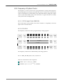
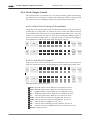
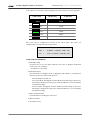
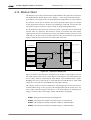
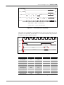
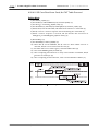
4.5. PREVIEW
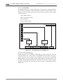
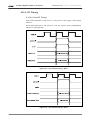
4.5.1. Preview Setup
The CL765 displays images entered from Camera on LCD. For the image display,
3Mega Pixel (2048x1536) is supported in maximum. In Preview mode, the area to
display on LCD is selected on the image entered from Camera. And the target is
set as same as the Display resolution of LCD. After the above setup is completed,
the CL765 converts the area selected in the original image of Camera to Preview
Resolution to display on LCD in use of Video scalar.
1. Select Source image by 2-pixel unit from the original image. In the register
setup of the CL765, StartX, StartY, Width and Height are selected from the
source image. The charged registers are 0x12, 0x13, and 0x9e.
2. Set the resolution of Target image as large as the display area of LCD. The
resolution unit of the target image is also 2-pixel. Set the target resolution to the
display image resolution. The charged registers are 0x15 and 0x9e.
3. Set Image Effect and the selected image effect is applied to Preview.
4. Set LCD Display Area, and the position previewed on LCD is set.
5. Set Preview at 0x00 command register.
Display Width ( 0X13, Bit[7:0] ) : 0XF0
Display Taret Width
( 0X14, Bit[7:0] ) : 0X3C
Display Start Address (0X12) :
0X0028
Original
Image
(640X480)
Source
Image
(480X480)
Display
Image
(120X120) Display Taret Height
( 0X15, Bit[15:8] ) : 0X3C
Display Height(0X13 Bit[15:8] : 0XF0
Figure 4-8. Preview Area Setup (VGA)
CORE LOGIC Proprietary and Confidential 41
Datasheet │ Doc. #: CLQP-DS-743
CL765 │ Camera Application Processor
BIT
D15
D14
D13
D12
D11
D10
D9
D8
D7
D6
D5
D4
D3
D2
D1
D0
W/R
Function
Default
Display
Start
Address
0x0028
Display
Width
0xf0f0
Display
Target
Size
0x3c3c
Display
Extension
Address
0x0000
Display(Preview) Start Address (0x12)
Display Y Start Address
BIT[15:0]
W/R
Display X Start Address
Display(Preview) Width(0x13)
Display Height
BIT[15:0]
W/R
Display Width
Display(Preview) Target Size(0x15)
Display Target Height
BIT[15:0]
W/R
Display Target Width
Display(Preview) Extension Address(0x9e)
Target Height
BIT[15:0]
Target Width
Y Width
W/R
X Width
42 Issue Date: 2004/11/05 │ CONFIDENTIAL
Y Start
X Start
www.corelogic.co.kr │
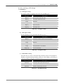
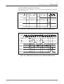
4.5.2. Preview Rotation
The CL765 supports rotation of Mirror, Flip, 90°, 180°, and 270° in Preview. With
simple register setup, Preview rotation is available. Preview rotation only
supports LCD Display and is not applied to JPEG Encoding. To use Rotation
function, it is necessary to set Preview area again. The relative register is 0x01.
Rotation Degree
Register
Image
Description
0x01
Original
Bit[4:2]: 3’b000
0x01
90
Rotation 90° clockwise
Bit[4:2]: 3’b001
0x01
180
Rotation 180° clockwise
Bit[4:2]: 3’b010
0x01
270
Rotation 270° clockwise
Bit[4:2]: 3’b011
CORE LOGIC Proprietary and Confidential 43
CL765 │ Camera Application Processor
Datasheet │ Doc. #: CLQP-DS-743
0x01
Flip Horizontal
Horizontal Flip
Bit[4:2]: 3’b100
Vertical Flip
0x01
(mirror)
Bit[4:2]: 3’b101
Flip Vertical
Table 4-4. Examples of Preview Rotation
4.5.3. Preview Frame Skip
Preview Frame Display interval is adjustable. Frames entered from Camera are
sampled and displayed on LCD. The relative register is 0x0f.
44 Issue Date: 2004/11/05 │ CONFIDENTIAL
www.corelogic.co.kr │
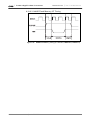
4.6. JPEG ENCODING
4.6.1. Still JPEG Encoding
Perform JPEG encoding by converting the image entered from Camera to the
various sizes. Camera image supports up to 3 Mega-Pixel(2048x1536). JPEG Codec
is JPEG Baseline method and supports Camera image of YCbCr 4:2:2 Format.
The capacity of the internal SRAM buffer is limited. Therefore JPEG file should be
read in use of Flow Control before the JPEG buffer which had been set while
decoding is over-flown.
JPEG Encoding is similar to Preview procedure. First, select the area encoded
from the original image entered from Camera and set JPEG Target resolution.
1. Select Source image by 4 pixel unit from the original image. In the register
setup of the CL765, StartX, StartY, Width and Height are selected from the
source image. Relative registers are 0x10, 0x11 and 0x9d.
2. Set Target image resolution by adjusting to JPEG Target. The resolution unit
of the target image is also 4-pixel. The relative registers are 0x14and 0x9d.
3. Set JPEG encoding at 0x00 command register.
4. Flow Control is used to prevent a buffer from overflow when the data size
exceeds the threshold of JPEG buffer, which had been already decided. Flow
Control is not necessary when file size is small because of slam JPEG Target
resolution. For more details, refer to the description in ‘Flow Control’ Part.
5. Completion of JPEG encoding. Interrupt is used to complete JPEG encoding.
For more details, refer to the description in ‘Interrupt’ Part.
6. JPEG File Read. To read JPEG file, two methods are used; to use Flow Control
and to read JPEG file after completing JPEG encoding. Fore more details on
JPEG file read, refer to the description in ‘SRAM Readʹ Part.
CORE LOGIC Proprietary and Confidential 45
Datasheet │ Doc. #: CLQP-DS-743
CL765 │ Camera Application Processor
BIT
D15
D14
D13
D12
D11
D10
D9
D8
D7
D6
D5
D4
D3
D2
D1
D0
W/R
Function
Default
JPEG
Window
Start
Address
0x0000
JPEG
Window
Width
0x78a0
JPEG
Window
Target
Size
0x78a0
JPEG Window Start Address (0x10)
Display Y Start Address
BIT[15:0]
W/R
Display X Start Address
JPEG Window Width(0x11)
Display Height
BIT[15:0]
W/R
Display Width
JPEG Target Size(0x14)
Display Target Height
BIT[15:0]
W/R
Display Target Width
JPEG Window Extension Address(0x9d)
BIT[15:0]
Y Target
X Target
JPEG
Window
Y Start
X Start
Extension
Address
W/R
Y Width
X Width
0x0000
4.6.2. JPEG Quality
It is available to adjust JPEG quality by adjusting Quantization Scale Factor
during JPEG encoding. In JPEG encoding, As smaller as the value of Quantization
Scale Factor is, the JPEG image quality gets better but the file size gets smaller.
Quantization Scale Factor is adjustable from 0x08 to 0x80.
46 Issue Date: 2004/11/05 │ CONFIDENTIAL
www.corelogic.co.kr │
4.6.3. MJPEG Encoding
The CL765 supports MJPEG. The CL765 internally has 256 kbyte SRAM. Among
the whole SRAM buffer, It is available to use the SRAM area except Video buffer
area as MJEPG buffer. MJPEG buffer can use the SRAM area except Preview
buffer. When only MJPEG buffer is used, MJPEG encoding time is limited by the
capacity of the buffer. This limitation on encoding time is free with using Flow
Control; available to encode MJPEG without any limitation on buffer capacity.
Followings show the order of MJPEG encoding.
1) MJPEG Resolution
2) MJPEG Time and JPEG Quality factor setup
3) Flow Control setup
4) MJPEG Encoding command setup
5) Memory Read according to Flow Control setup
6) MJPEG encoding completion and SRAM Read completion
MJPEG is configured with the series of JPEGs. The CL765 supports following 2
architectures.
1) Architecture that shares Header
It is available to reduce the whole size by sharing the header of each frame.
HEADER
BODY
BODY
∙∙∙∙∙∙
BODY
BODY
∙∙∙∙∙∙
2) Architecture that does not share Header
File size gets larger since the header of each is used.
HEADER
BODY
HEADER
4.6.4. OSD Encoding
When OSD encoding is performed in OSD Preview, JPEG is encoded as much as
Preview size. When OSD capture is performed, the image same with the OSD
Preview screen is encoded. Followings show the order of OSD encoding.
1) OSD Preview.
2) JPEG Quality factor setup
3) OSD Encoding
CORE LOGIC Proprietary and Confidential 47
CL765 │ Camera Application Processor
Datasheet │ Doc. #: CLQP-DS-743
4.7. JPEG DECODING
The CL765 can decode JPEG file of Baseline format, the most used among JPEG
formats. It is available to decode images up to VGA in maximum. Followings are
the YCbCr formats supported.
-. YCbCr
4:4:4
-. YCbCr
4:2:2
-. YCbCr
4:1:1
-. YCbCr
4:2:0
4.7.1. Still JPEG Decoding
JPEG Decoding supports resolution up to 3 Mega-Pixel in maximum. In case the
size of JPEG file is larger than the capacity of the JPEG buffer, it should be
decoded in use of Flow Control. For the JPEG buffer size, it is available to use the
whole SRAM area except Video buffer area (If OSD Preview is used, OSD Buffer
area should be also excluded from JPEG buffer area). Followings are the order of
JPEG Decoding.
1) JPEG Resolution check: check the JPEG resolution in use of S/W.
2) Select the decoding area according to JPEG Resolution.
3) If the size of JPEG file is larger than JPEG buffer area, Flow control should be
used.
4) Perform JPEG Decoding and setup Register 0x00.
5) Read data of JPEG File in use of Flow Control.
6) Complete JPEG file Flow Control and Decoding.
4.7.2. MJPEG Decoding
MJPEG Decoding procedure is same with Still JPEG Decoding procedure.
Followings are the order of decoding.
1) MJPEG Resolution check: checks JPEG Resolution in use of S/W.
2) Select decoding area according to MJPEG Resolution.
3) If the size of MJPEG file is larger than JPEG buffer area, Flow control should
be used.
4) Perform MJPEG Decoding and setup Register 0x00.
5) Read data of MJPEG File in use of Flow Control.
6) Complete MJPEG file Flow Control and Decoding.
48 Issue Date: 2004/11/05 │ CONFIDENTIAL
www.corelogic.co.kr │
4.8. SRAM BUFFER SETUP
The CL765 has internally SRAM of 256KByte and the SRAM is classified into its
purpose for use. SRAM Read/Write is performed by 2btye unit. SRAM buffer
areas are Video buffer area, OSD buffer area, and PIP buffer area. Each buffer area
is used only when the relevant functions are used, so it is available for each buffer
to share SRAM area. Following description details each buffer.
1) Video Buffer
Scales down the size of images entered from Camera according to Preview
setup and save. When one frame is completed in Camera, Video buffer
writes data on LCD. The capacity of Video buffer should be set according to
Preview Resolution.
a) Video buffer capacity
If Preview is 128 x 160, Video buffer should be set to 40K byte SRAM area.
b) Data format
Data is saved in Video buffer as YCbCr 4:2:2 format transmitted by
Camera.
2) OSD Buffer
OSD Buffer saves OSD BMP image. The capacity of OSD buffer depends on
OSD Resolution and the maximum capacity is same with that of Video
buffer. In OSD buffer, OSD1 area is set separated from OSD2 area. If OSD
Menu is used, it is available to use OSD1 and OSD2 Buffers.
3) PIP Buffer of CL765
PIP buffer is the SRAM area that saves PIP data. The capacity of PIP buffer
depends on PIP Resolution. In PIP, 4bit is data of 1 pixel and 16bit is data of
4 pixels. Generally, if PIP is set to 128x16, 1K byte is required as a PIP buffer
area.
Following Figure shows the example of SRAM buffer setup. This is the case that
Preview Resolution is set to 128*128, OSD1 and OSD2 buffers are set to 128*16,
and PIP buffer is set to 128*16.
SRAM buffer should be initialized according to Preview, OSD, and PIP setup
when starting Camera Mode. Also, the point of each buffer should be changed in
operating Camera Mode for efficient use of Memory.
CORE LOGIC Proprietary and Confidential 49
CL765 │ Camera Application Processor
Datasheet │ Doc. #: CLQP-DS-743
Figure 4-9. Example of SRAM Buffer Setup
4.9. SRAM READ
Describes how to read data from SRAM in the CL765. This is used to read SRAM
for JPEG,MJPEG encoding and Video buffer read. This chapter describes the case
that Flow Control is not used.
a) SRAM address Point setup
b) 0x0b setup for Index Register
c) Data Port Read
4.10. SRAM WRITE
Describes how to write data in SRAM in the CL765. This is used to write in SRAM
for JPEG, MJPEG decoding, OSD data write and PIP data write. This chapter
describes the case that Flow Control is not used.
a) SRAM address point setup.
Set SRAM start address in Register 0x09 and 0x0A.
b) Set Index Register 0x0b.
c) Data Port Write.
50 Issue Date: 2004/11/05 │ CONFIDENTIAL
www.corelogic.co.kr │
4.11. PIP (PICTURE IN PICTURE)
PIP is a function that inserts a specific icon or text image in JPEG images while
performing JPEG encoding. Also, like OSD, it is available to display PIP image on
Preview. PIP supports 8 Color Tables and each Color Table is configured as YCbCr
4:2:2. It is available to use various colors in PIP by changing the table values.
For PIP, 1 pixel consists of 4bits and 16bit data is configured with 4 pixels. Each 4bit sets PIP enable bit and PIP table. When PIP enable bit is “Set”, PIP image is
displayed. After displaying PIP image, Camera image is displayed.
PIP Table Number
Bit 3
Bit 2
Enable
Bit 1
Bit 0
Figure 4-10. Bit Configuration of PIP Pixel Data
If Bit0 is 1, the color is decided in use of Bit[3:1]. For example, Bit[3:1] is 000, the
color set in Register 0xa8 is referred.
Bit[3:1] Value
Reference Register
000
0xa8
001
0xa9
010
0xaa
011
0xab
100
0xac
101
0xad
110
0xae
111
0xaf
CORE LOGIC Proprietary and Confidential 51
Datasheet │ Doc. #: CLQP-DS-743
CL765 │ Camera Application Processor
Color Table is set as follows. The configuration of 0xa8~0xaf is as following table.
Y 6Bit [15:10]
Cb 5Bit [9:5]
Color
Cr 5Bit [4:0]
Value
White
0xFE10
Blue
0x6298
Red
0x659B
Green
0x9906
Yellow
0xD872
Purple
0x6298
The colors can be configured as shown in the above table. The colors are
configured by referring the following formula.
Y
=
0.299R + 0.587G + 0.114B
Cb
=
-0.1687R – 0.3313G + 0.5B + 128
Cr
=
0.5R – 0.4187G – 0.0813B + 128
1) PIP under Preview Mode
a) PIP Table Setup
Set PIP Color in use of 8 tables. Indicate each color to Register 0xa8-0xAF
and 8 colors are available.
- Examples of color setup
b) PIP Mode Setup
Set PIP Mode. Set Register 0x18 to BIT[10:8]. PIP Mode is classified into
Normal, Overwrite, and Overlay preview.
-
Normal Mode: Turn PIP off.
Overwrite Mode: distinguish Camera Mode from PIP image. In Preview,
PIP image is displayed on the pixels where Enable bit is “Set” in PIP data
for JPEG encoding.
- Overlay Mode: distinguish Camera Mode from PIP image. In Preview,
PIP image is displayed on the pixels where Enable bit is “Set” in PIP data
for JPEG encoding
c) PIP Coordinate Setup
Position PIP for LCD display in Preview.
d) PIP Data Write
e) Perform Preview.
52 Issue Date: 2004/11/05 │ CONFIDENTIAL
www.corelogic.co.kr │
4.12. FLOW CONTROL
Flow Control enables to capture or playback still images or moving pictures by
using a small memory efficiently. In the existing method, as data is not readable
until all of the captured JPEG images are saved in the memory, it is unavailable to
capture the image of which capacity exceeds the memory capacity. But with Flow
Control, the host can simultaneously read data from the memory as writing
captured JPEG data in the memory. Therefore, Flow Control can process any JPEG
images regardless of the size and capacity of images (However, there is a
limitation in I/O read/write speed of the host). Also, as there is no limitation on
the internal memory when taking the moving pictures, it is available to take
moving pictures without time and capacity limitation.
4.12.1. Detailed Description on Flow Control Architecture
The architecture of Flow Control is similar to Circular Queue; the beginning of a
memory is connected to the end. Therefore there is no limitation on the size of
JPEG data.
To use Flow Control, it is required to decide how much memory is used. The 16bit
FIFO size register shows the size of memory to be used. For example, when the
value of the register is 0x5000, that means 0x5000=20480 (Word). In this case,
40Kbyte is usable. If the size of data is larger than the FIFO size, the exceeding
data is automatically taken by Register 0. Therefore the host does not request
additional process or devices.
In case of encoding that captures images, if the host reads the encoded data as
soon as data is encoded in the memory, the amount of readable data in the
memory is not enough. Then the process of read and halt should be repeated.
JPEG Threshold size setting solves this problem; the data processing is not started
until a specified size of data is saved in the memory and the specified size is JPEG
Threshold size. For example, set JPEG Threshold size at 0x2000 (16Kbyte) and
send JPEG Capture command, and the encoding data is saved in the memory.
When the saved data size reaches to the JPEG Threshold size which has been set
in advance, JPEG Threshold interrupt is generated. Then the interrupt is notified
to the host and the host starts to read the memory. The JPEG Threshold interrupt
is generated when the JPEG Threshold size is same with the interval size between
the point where data is written and the point where the host starts to read in the
memory. Therefore, this interrupt can be generated even while the processing is
going on as well as the first reaching.
When using this Flow Control, a critical problem may occur if one process (Write
process or Read process) is quicker than the other process. In other words, new
data can be overwritten on the existing data before the host reads the existing data
when Write process is quicker than Read process during Image Capture process.
Reversely, the read data can be read again when the host reads data quicker than
Write process. To solve these problems, two margins are made;
Underflow/Overflow Margin. The Underflow margin is generated when the Read
speed is quicker than the Write speed and the interval between the write point
and the read point is within a certain range. The host should halt the Read process
CORE LOGIC Proprietary and Confidential 53
Datasheet │ Doc. #: CLQP-DS-743
CL765 │ Camera Application Processor
for a while to avoid Underflow when the Underflow Margin interrupt is
generated. The Overflow margin is generated when the Write speed is quicker
than the Read speed and the interval between the write point and the read point is
within a certain range. The host should accelerate the Read speed when Overflow
margin is generated. If the Overflow occurs, the host should generate Error for the
overflow.
Also, as there is a register which shows the current point of write/read of FIFO
memory, it is available to calculate the amount of data to write or read.
As Threshold, Underflow margin and Overflow margin in the above are for users
to encode/decode JPEG easily in use of Flow Control, they are not the required
items to use.
There can be many ways to implement Flow Control. But the following method is
optimized for Flow Control.. Therefore, there will be no problem with the
following method.
Figure 4-11. Flow Control
✑
Notes
●
Hynix VGA Sensor (640x480). 32fps
●
FIFO Size: 40Kbyte
●
I/O TCLK: about 420ns
●
Stable Encoding as a 140Kbyte JPEG Data
54 Issue Date: 2004/11/05 │ CONFIDENTIAL
www.corelogic.co.kr │
4.12.2. Modem CPU Requirement
Encoding/Decoding in use of Flow Control is performed in real-time. So, if the
memory access time of Modem CPU is late, Overflow or Underflow can occur.
Therefore, Modem CPU should quickly write or read data in the memory to
prevent Overflow or Underflow.
In case of Encoding, following factors can have the influence upon Flow Control:
FIFO size, I/O 1 cycle time, and JPEG data size. It is hard to predict JPEG data size
exactly because the complexity of the image received from the sensor or JPEG
quality factor have the influence upon JPEG data size. But in general, for VGA
(640x480), JPEG data size is 120-140Kbytes in the worst case. So if the encoding
test is performed with the worst case, normal images will have no problem. FIFO
size and I/O 1 cycle time (TCLK) can be set in Modem CPU and the values will be
got from several tests.
Following table shows the test result in use of VGA sensor.
●
Hynix VGA Sensor (640x480), 32fps.
FIFO Size
40KB
40KB
64KB
64KB
I/O TCLK
420ns
680ns
420ns
680ns
140KB
107KB
over 140KB
130KB
Max JPEG
Size
Table 4-5. Examples of Preview Rotation
This result can be influenced by the CPU and other factors but will not be
changed much. Refer to the test result to set FIFO Size and TCLK.
Encoding/Decoding in use of Flow Control is implemented by polling. So data
may be not read/written in time when interrupts occur from Modem CPU in
operation. Therefore, it is recommended to block interrupts before starting
encoding/decoding.
CORE LOGIC Proprietary and Confidential 55
Datasheet │ Doc. #: CLQP-DS-743
CL765 │ Camera Application Processor
4.12.3. Flowchart & Pseudo Code
Figure 4-12. Encoding Flowchart
Error #1 – This error cannot occur in the normal status. If it has occurred, check if the
register setup is correct.
Error #2 – This error means that an overflow has occurred. It can occur when FIFO
size is set too small or JPEG Quality factor (Q factor) is set too low. In this
case, make the FIFO size larger or Q factor higher.
56 Issue Date: 2004/11/05 │ CONFIDENTIAL
www.corelogic.co.kr │
Encoding Pseudo Code
U16 Sara_FlowStillCapture(U16 *stillImg, U32 *stillsize)
{
Define the variables.
CamStatusSetMode();
// Status Register Clear. must.
FlowSetRegSize();
// Set a Flow control register
DoCameraOperation(Sara_STILL_CAPTURE); // Do Still Capture
// Encoding Start -> Wait , JPEG Encode End Or write pointer is over thre_pos
while(1)
{
cmd_status = CamCommandStatus();
write_ptr = FlowGetWriteAddress();
if((cmd_status != 0) || (write_ptr >= thre_pos) ) break;
}
if(cmd_status isn’t a zero)
{
// JPEG Encoding Done or Error
if(cmd_status isn’t encoding done)
Error Processing. Return.
If(flow status == Overflow)
Error Processing. Return
*stillsize = Flow_EncodeDone(stillImg, read_size);
Terminate Operation.
return TRUE;
}
DoCameraOperation(Sara_STILL_CAPTURE|Sara_DO_STILL_UPLOAD);
Read a WP register. Read the data.
while(1)
{
flow_status = FlowInterruptStatus();
cmd_status = CamCommandStatus();
if(cmd_status isn’t a zero)
{
// JPEG Encoding Done or Error
if(cmd_status isn’t encoding done)
Error Processing. Return.
if(flow status == Overflow)
Error Processing. Return
*stillsize = Flow_EncodeDone(stillImg, read_size);
Terminate Operation.
return TRUE;
}
if(flow status isn’t a zero)
Error Processing. Return
Calculate a size for reading.
Read the Data.
CORE LOGIC Proprietary and Confidential 57
Datasheet │ Doc. #: CLQP-DS-743
CL765 │ Camera Application Processor
}
return 0;
Figure 4-13. Decoding Flowchart
Error #1 – This error cannot occur in the normal status. If it has occurred, check if the
register setup is correct.
Error #2 – This error means that an underflow has occurred. It can occur when FIFO
size is set too small or writing speed is low. In this case, make the FIFO size
larger or speed up the writing by adjusting CS timing of the external I/O.
58 Issue Date: 2004/11/05 │ CONFIDENTIAL
www.corelogic.co.kr │
Decoding Pseudo Code
U16 Sara_FlowStillDecode(U16 *stillImg, U32 stillsize)
{
Define the variables.
CamStatusSetMode();
FlowSetRegSize();
// Status Register Clear. must.
// Set a Flow control register
CamSRAMWritePath_Still(); // Open the memory path from host to Sara
//Check data size for writing
if(FIFO Size >= wordSize)
{
Write a Data.
DoCameraOperation(Sara_DO_STILL_DECODE); // Decoding
Waiting for Decoding Done.
return TRUE;
}
else
Write a data as FIFO Size.
// Do Decoding.
DoCameraOperation(Sara_DO_STILL_DECODE|Sara_DO_STILL_DOWNLOA
D);
timeout=0;
while(1)
{
if(cmd_status isn’t zero )
Error Processing. return;
if(flow status is overflow or underflow)
Error Processing. Return.
Calculate a data size for writing.
Write a data.
if(writing for all data)
Terminate Decoding.
Return TRUE
CORE LOGIC Proprietary and Confidential 59
CL765 │ Camera Application Processor
Datasheet │ Doc. #: CLQP-DS-743
4.13. DISPLAY UNIT
The Display Unit of the CL765 includes alpha-blender and output device interface.
The alpha-blender blends input source images – video image and OSD images –
and compose one image which will be displayed on output devices, LCD’s and TV.
For external visual device interface, the CL765 provides three types of external
visual equipment interfaces: 80-Type LCD, RGB-Type LCD and TV encoder. The
selection of output visual device type is made by programming REG_0x72.
For LCD interface, the CL765 can control two LCD’s – generally one for main-LCD
and the other for sub-LCD. The interface consists of common data and control
signals (18-bit data bus and read/write strobes) and dedicated chip selects for each
LCD. The two LCD’s can be activated exclusively: they share data bus and control
signals, and hence they can not be activated at the same time.
Internal Memory
80_ type
LCD
Controller
to 80_ type LCD
OSD 2
RGB_type
LCD
Controller
to RGB_ type LCD
OSD 1
CCR656/601
Controller
to TV encoder
Video_image
Frame
Background
DISPLAY UNIT
Figure 4-14. Data-flow of Display Unit
Figure 4-16 shows the data-flow of Display Unit. Inputs to the Display Unit are
one video image in 4:2:2-YUV format and two OSD images. The OSD bitmaps are
one of three formats: 8bit-indexed, 4444-αRGB, and 565-RGB. Before alphablending, the source video image is converted into 18-bit RGB format, while OSD
images are converted into 18-bit RGB with 4-bit alpha channel.
The Display Unit has layered architecture: The background is the bottom-layer
and the OSD2 image is the top-layer. The Background and the Frame layer are
only visible when the output visual device is TV. The sequence of making result
image is as follows (For LCD output, STEP1 and STEP2 are skipped):
STEP1 : Background and Frame are multiplexed
STEP2 : The image after STEP1 and video image are multiplexed
STEP3 : The image after STEP2 and OSD1 image are alpha blended
STEP4 : The image after STEP3 and OSD2 image are alpha blended
60 Issue Date: 2004/11/05 │ CONFIDENTIAL
www.corelogic.co.kr │
For multiplexing of the sequence, following operation is used:
if (current_position is within FG image area) {
RDST = RFG
GDST = GFG
BDST = BFG
}
else {
RDST = RBG
GDST = GBG
BDST = BBG
}
For alpha blending of above operation, following equation is used:
RDST = RFG x α + RBG x (1 – α)
GDST = GFG x α + GBG x (1 – α)
BDST = BFG x α + BBG x (1 – α)
Video Image
Image on display device
OSD Image
α
CORELOGIC
α=0
α=0.5
α=1.0
CORELOGIC
Figure 4-15. Example of Alpha-blending
Where RBG, GBG and BBG are color components of image that is calculated in
previous operation step, while RFG, GFG and BFG are color components for image of
current layer. There is four bit fixed-point arithmetic value and its range is 0 to 1.
During the operation, for TV output case, the video image for the process is scaled
to 2X in direction of both.
CORE LOGIC Proprietary and Confidential 61
Datasheet │ Doc. #: CLQP-DS-743
CL765 │ Camera Application Processor
After alpha blending, the result image is displayed on output visual device
through provided output device interfaces: 80-Type LCD interface, RGB-Type
LCD interface and external TV encoder interface. The output visual device
interfaces share common physical pins of the CL765, and hence only one device
can be activated at a time.
4.13.1. Data Format of OSD Image
The CL765 provides three types of bitmap formats for OSD. They are 8bit-indexed,
4444-αRGB, and 565-RGB format. The 8bit-indexed format consists of 3-bit alpha
channel and 5-bit color index. The 5-bit color index is used to fetch color
component from Color Lookup Table (CLUT): CLUT has 32 entries of 16-bit color
component in 565-RGB format. Compare to other OSD bitmap format, 8bitindexed format saves required memory space for OSD image since it needs one
byte per pixel, while other format requires two bytes per pixel.
The bitmap in OSD buffer is expended to 18-bit (666-RGB) color component with
4-bit alpha channel either by CLUT or by bit expansion logic.
4.13.1.1. 8Bit-indexed Format
For 8bit-indexed format, R, G and B component of each pixel are from CLUT
entries indexed by lower 5 bits of input data. The resulting 4-bit alpha value is
made from input upper 3bits. Figure 4-18 shows the logical operation of bit
expansion by using CLUT for 8bit-indexed OSD case.
C_INDEX = bit[4:0]
R[5:0] = {CLUT[C_INDEX][15:11], CLUT[C_INDEX][15]}
G[5:0] = CLUT[C_INDEX][10:5]
B[5:0] = {CLUT[C_INDEX][4:0], CLUT[C_INDEX][4]}
b7
b6
A_INDEX
b5
alpha
expansion
a[3:0]
b4
b3
CLUT(Color Lookup Table)
C_INDEX
b2
31 R[4:0]
G[5:0]
B[4:0]
b1
30 R[4:0]
G[5:0]
B[4:0]
b0
29 R[4:0]
G[5:0]
B[4:0]
0 R[4:0]
G[5:0]
B[4:0]
8- bit index color
16- bit to 18 - bit
expansion
R[4:0]
R[4]
G[5:0]
result 18 - bit color
Figure 4-16. The Bit Expansion for 8Bit-index Color
62 Issue Date: 2004/11/05 │ CONFIDENTIAL
B[4:0]
B[4]
www.corelogic.co.kr │
The alpha expansion, shown in Figure 4-18, is performed by referencing the
hardwired-expansion-table. The table contents are listed in Table 4-8. For an
example, When A_INDEX is 3 then result α is 4-bit 0110, i.e., 6 in integer and 0.4
(= 6/15) in fixed-point.
C_INDEX[2:0]
Result α[3:0]
0
0
1
2
2
4
3
6
4
8
5
10
6
12
7
15
Table Table 4-6.
Alpha Expansion Table
4.13.1.2. 4444-αRGB Format
For 4444-αRGB format, R, G and B component of each pixel are constructed by bit
expansion logic operation as shown in Figure 4-19 (α is from input pixel data
without bit expansion):
α[3:0] = bit[15:12],
R[5:0] = {bit[11:8], bit[11:10]}
G[5:0] = {bit[7:4], bit[7:6]}
B[5:0] = {bit[3:0], bit[3:2]}
b15
b14
α[3:0]
b13
b12
b11
b10
B[3:0]
b9
b8
b7
b6
G[3:0]
b5
b4
b3
b2
R[3:0]
b1
b0
4444- αRGB color
4- bit to 6 - bit
expansion
4- bit to 6 - bit
expansion
4- bit to 6 - bit
expansion
R[5:0]
G[5:0]
B[5:0]
b[3:0]
b[1:0]
b[7:4]
b[7:6]
b[11:8]
b[11:10]
α[3:0]
Figure 4-17. The Bit Expansion for 444-αRGB Color
CORE LOGIC Proprietary and Confidential 63
Datasheet │ Doc. #: CLQP-DS-743
CL765 │ Camera Application Processor
4.13.1.3. 565-RGB
For 565-RGB format, R, G and B component of each pixel are constructed by bit
expansion logic operation as shown in Figure 4-20. For the format alpha value of
each pixel is not available. Instead, the value of REG_0x18[7:4] is used as alpha
value for all pixels.
α[3:0] = REG_0x18[7:4]
R[5:0] = {bit[15:11], bit[15]}
G[5:0] = bit[10:5]
B[5:0] = {bit[4:0], bit[4]}
b15
[7:4]
RGB18
b14
b13
b12
b11
b10
b9
b8
b7
b6
b5
b4
b3
b2
b1
b0
565- RGB color
5- bit to 6 - bit
expansion
b[4:0]
5- bit to 6 - bit
expansion
b[4]
b[10:5]
b[15:11]
b[15]
α[3:0]
Figure 4-18. The Bit Expansion for 565-RGB Color
4.13.1.4. Chroma-keying
Chroma-keying is one of methods compositing two source images into one. The
function checks if the current pixel of foreground bitmap matches to the predefined color (the value of REG_0x19) and replaces it to pixel from background
bitmap (Figure 4-21). For SARA, besides alpha-blending, chroma-keying is also
provided. For 8bit-indexed bitmap, the pixel data after CLUT is used to compare
to REG19, while pixel data from source bitmap is used for 4444-αRGB and 565RGB format.
64 Issue Date: 2004/11/05 │ CONFIDENTIAL
www.corelogic.co.kr │
Video Image
Image on display device
OSD Image
CORELOGIC
?
REG_0x19
CORELOGIC
color = REG_0x19 (i.e., chroma-key color)
Figure 4-19. Chroma-keying
CORE LOGIC Proprietary and Confidential 65
Datasheet │ Doc. #: CLQP-DS-743
CL765 │ Camera Application Processor
4.13.2. 80-Type LCD Interface
The CL765 can control two LCD’s, one for main-LCD and the other for sub-LCD.
Figure 4-22 shows the generic connections between the CL765 and LCD’s.
L_CS_N
L_ADS
L_RD_N
Main LCD
L_WR_N
L_DA[17:0]
CL765
LS_CS_N
Sub LCD
Figure 4-20. The Generic Interconnection to LCD Modules
The pins used in the interconnection are:
L_DA[17:0]: 18-bit data bus for LCD’s register and GRAM data read/write
L_RD_N: read strobe to LCD’s, active-low
L_WR_N: write strobe to LCD’s, active-low
L_ADS: address and data selection signal. During bus cycle, it remains high
for data and low to address.
L_CS_N: chip select for main-LCD, active-low
LS_CS_N: chip select for sub-LCD, active-low
For 80-Type LCDs, the CL765 supports various LCDs such as 260K, 65K, and 4K
and various buses such as 16bit, 18bit, 9+9, and 8+8. The CL765 sets LCD
Windows every Frame Preview and writes GRAM.
The CL765 stores the scaled Data from Camera to the Video Buffer. Once 1frame
of data has been stored in the Video Buffer, the rest of the Data gets updated fast
into LCD GRAM using similar method such as Burst mode in LCD. The filling
method is different for various types of LCD Driver IC but following is an
example.
66 Issue Date: 2004/11/05 │ CONFIDENTIAL
www.corelogic.co.kr │
VSYNC
L_CS_N
L_ADS
L_WR_N
L_DA[17:0]
CMD0
CMD1
CMD2
CMDn
L_DA0 L_DA1 L_DA2 L_DA3 L_DA4
L_DAn
- CMD0, CMD1 .... CMDn : LCD Command
- L_DA0, L_DA1 ..... L_DAn : LCD Gram Data
Figure 4-21. Camera Mode and LCD_Display
The CL765 sets commands for LCD display in use of two ways; the one is to set
parameters in commands; and the other is to set LCD commands and parameters
to display on LCD as decided sequence.
SCLK
L_CS_N
TCS
L_WR_N
TWR1
TWR2
TWR3
TADS2
TADS3
L_ADS
TADS1
LCD_DATA
L_DA[17:0]
LCD_DATA
TL_DA
Figure 4-22. LCD Command/Parameter Set Timing
Description
symbol
Min
CS setup time
Tcs
5ns
WR setup time
TWR1
1*SCLK + 5ns
WR low period
TWR2
4*SCLK
WR high period
TWR3
3*SCLK
ADS setup time
TADS1
6ns
ADS low period
TADS2
6*SCLK
ADS high period
TADS3
1*SCLK
DATA setup time
TL_DA
6ns
Typ
max
Table 4-7. LCD Command/Parameter Set Timing Table
CORE LOGIC Proprietary and Confidential 67
Datasheet │ Doc. #: CLQP-DS-743
CL765 │ Camera Application Processor
The above figure shows the timing diagram of the level to set LCD commands
and parameters in LCD Interface. According to the characteristics of the LCD, the
polarity of L_ADS can be changed. However, the overall timing of LCD
Command/Parameter setup is the above. The values shown in the above table are
the timing of internal operation and it is no need for the host to set values for
them.
SCLK
L_CS_N
L_WR_N
5ns
L_DA[17:0]
L_DA[17:0]
4.5ns
Figure 4.23. LCD Gram Data Write Timing
The above is LCD Gram Data Write Timing diagram. The Low/High section of
L_WR_N is adjustable by setting registers.
68 Issue Date: 2004/11/05 │ CONFIDENTIAL
www.corelogic.co.kr │
4.13.2.1. 80-Type LCD Setup
1. LCD Setup 1
a) LCD Type 1 Setup
Set register values according to the LCD color and Bus type.
LCD Type 1
Description
BIT[1:0]
BUS type setup: 8bit, 16bit, 18bit
BIT[4:2]
Color Depth: 260K, 65K,4K, 256
BIT[5]
RGB Order
BIT[6]
RGB Data align
BIT[8:7]
Write Low Period
BIT[10:9]
Write High Period
Table 4-8. LCD Type 1 Setup
b) LCD Type 2 Setup
Set the method to send commands and data to LCD.
LCD Type 2
BIT[2:0]
Description
18bit data formatting in 260K color and 16/8 bit Bus.
BIT[3]
Reserved
BIT[5]
Reserved
BIT[8]
Write commands in 8+8 interface.
BIT[9]
Write parameters in 8+8 interface.
BIT[12:10]
LCD Command Align
Table 4-9. LCD Type 2 Setup
c) LCD Window Setup
Describes how to set the commands and parameters that set LCD Windows.
Window command and parameter setup for LCD display positioning is
varied according to the type of LCD Driver IC.
Window Setup
Description
REG 0x40
Set Window Write system and Write Cycle.
REG 0x41
Window X position setup command
REG 0x42
Window Y position setup command
Table 4-10. LCD Window Setup
CORE LOGIC Proprietary and Confidential 69
Datasheet │ Doc. #: CLQP-DS-743
CL765 │ Camera Application Processor
d) LCD GRAM Setup
After completing LCD Window setup, LCD GRAM Write is performed.
GRAM start address setup can be varied by LCD Driver. Also, GRAM write
command can be optional. In the CL765, it is available to set all above cases
in use of Register 0x46.
Window Setup
Description
REG 0x46
Set GRAM Start address and GRAM Write.
REG 0x47
GRAM Start address Command setup
REG 0x48
GRAM Write command setup
GRAM Start position setup
REG 0x49
(in case Register 0x46 is set by User Defining).
Table 4-11. LCD GRAM Setup
2. LCD Setup 2
a) LCD type1 and Type2 are same with LCD setup 1
b) LCD Window/GRAM Setup
0xB5
Description
BIT[0]
New Mode setup: use LCD setup 2.
BIT[1]
8/9 Bit Interface: write command and parameter twice.
Window Write Cycle setup: Window Command/
BIT[7:2]
Parameter Write Cycle: Each command and parameter is
assigned to Register 0xC0-0xCF.
GRAM start address/GRAM Write Command Write Cycle setup:
BIT[13:8]
Set GRAM start address and Write
Command in Register 0xD0-0xD9
Table 4-12. LCD Window/GRAM Setup
c) ADS Polarity
ADS Polarity
Description
Window Command/Parameter ADS Polarity setup: set ADS
0xB6
polarity of each register when using Register 0xC0 ~ 0xCF.
REG 0xC0 =0xB6[0], 0XC1=0xB6[1] ……..0xCF=0xB6[15]
GRAM start address/Write command ADS Polarity setup: set
0xB7
ADS polarity of each register when using Register 0xD0~0xD9.
REG 0xD0 =0xB6[0], 0XD1=0xB6[1] ……..0xD9=0xB6[9]
Table 4-13. ADS Polarity
70 Issue Date: 2004/11/05 │ CONFIDENTIAL
www.corelogic.co.kr │
d) LCD Windows/Parameter Setup
Set LCD Window Command/parameter in Register 0xC0-0xCF. The cycle of
each command and parameter is set in Register 0xB5[7:2] and ADS Polarity
is set in Register 0xB6.
e) LCD GRAM Start Address/Write Command Setup
Set GRAM start address and Write Command in Register 0xD0-0xD9. The
whole cycle is set in Register 0xB5[13:8] and ADS Polarity is set in Register
0xB7.
f) Examples of LCD Setup
Following table shows the examples that use HD66773, Hitachi LCD Driver.
- 16Bit Bus, 65K color.
- LCD Window/GRAM Write setup
LCD
Description
ADS polarity
0x16
Horizontal RAM Address Position
0
X Parameter
X End and X Start
1
0x17
Vertical RAM Address Position
0-
Y Parameter
Y End and Y Start
1
0x21
RAM Address Set
0
GRAM start address
GRAM X start, Y start address
1
Command/Parameter
0x22
0
Table 4-14. Example of LCD Setup
- Windows setup Cycle
4 Cycle (0x16, 0x17 Command and Parameter Write cycle)
- GRAM Start address/GRAM write setup Cycle
3 Cycle (0x21 and Parameter 0x22)
CORE LOGIC Proprietary and Confidential 71
Datasheet │ Doc. #: CLQP-DS-743
CL765 │ Camera Application Processor
ⅰ) LCD Type 1
LCD Type 1
BIT[1:0]
BIT[4:2]
BIT[5]
BIT[6]
Value
‘01’
Remarks
= 16 bit BUS
‘100’ = 65K color
‘0’
‘0’
= RGB
Changeable according to LCD Panel.
= left-align
N/A for 16 bit Bus
BIT[8:7]
‘00’
= 1 clock
Changeable depending on the input clock.
BIT[10:9]
‘00’
= 1 clock
Changeable depending on the input clock.
REG 0x38
0x0011
Table 4-15. LCD Type 1
ⅱ) LCD Type 2
LCD Type 2
Value
Remarks
BIT[2:0]
‘000’
Set in 260K and 16/9/8 bit interface
BIT[3]
‘0’
Reserved
BIT[5]
‘0’
Reserved
BIT[8]
‘0’
Set in 8+8/9+9 Interface, depending on the
conditions.
BIT[9]
‘0’
Set in 8+8/9+9 Interface, depending on the
conditions.
BIT[12:10]
‘000’
Changeable depending on the way to give
command.
REG 0x39
0x0000
Table 4-16. LCD Type 2
ⅲ) 0xB5 Setup
0xB5
Value
Description
BIT[0]
‘1’
Use “LCD setup 2”.
BIT[1]
‘0’
Used by some part of 8+8/9+9 setup.
BIT[7:2]
‘011’
Gram start address/GRAM write command Set
Cycle, 3 cycle
BIT[13;8]
‘100’
REG setup value
0X040d
LCD Windows setup cycle. 4 cycle
Table 4-17. 0xB5 Setup
72 Issue Date: 2004/11/05 │ CONFIDENTIAL
www.corelogic.co.kr │
ⅳ) 0xB6 Setup
0xB7
Value
Description
BIT[0]
‘0’
ADS Polarity of LCD command 0x16
BIT[1]
‘1’
Parameter ADS Polarity of LCD command 0x16
BIT[2]
‘0’
ADS Polarity of LCD command 0x17
BIT[3]
‘1’
Parameter ADS Polarity of LCD command 0x17
REG setup value
0X0A
Table 4-18. 0xB6 Setup
ⅴ) 0xB7 Setup
0xB7
Value
Description
BIT[0]
‘0’
ADS Polarity of LCD command 0x21
BIT[1]
‘1’
Parameter ADS Polarity of LCD command 0x21
BIT[2]
‘0’
ADS Polarity of LCD command 0x11
REG setup value
0X02
Table 4-19. 0xB7 Setup
ⅵ) 0xC0-0xCF Setup
Register
Value
ADS Polarity
Description
0xC0
0X16
0
Horizontal RAM Address Position
0xC1
0Xxxxx
1
Horizontal start, end
0xC2
0X17
0
Vertical RAM Address Position
0xC3
0Xxxxx
1
Vertical Start, end
Table 4-20. 0xC0-0xCF Setup
ⅶ) 0xD0-0xD9 Setup
Register
Value
ADS Polarity
Description
0xC0
0x21
0
RAM Address Set
0xC1
0Xxxxx
1
RAM start address
0xC2
0X22
0
RAM Write command
Table 4-21. 0xD0-0xD9 Setup
CORE LOGIC Proprietary and Confidential 73
Datasheet │ Doc. #: CLQP-DS-743
CL765 │ Camera Application Processor
4.13.2.2. LCD Update under Camera Mode
1) LCD Lock
The CL765 has the overall control authority of the LCD when CL765 is
Camera mode, Therefore, the CL765 performs the displaying onto LCD once
it receives scaled Camera Data or encoding/decoding of the compressed
image. If MCU must access the LCD at this point, may use LCD LOCK
function to get override authority to access the LCD from the CL765. With
LCD Lock, CPU can directly access LCD under Camera Mode. LCD LOCK is
set by setting REG 0x3B to “0x01”. If LCD is not unlocked after setting LCD
Lock, the CL765 cannot display images on LCD. Therefore, CPU should
unlock LCD.
a) LCD Frame update interrupt check
If the CL765 perform LCD Lock while updating images on LCD, display
of one frame is stopped. To prevent this, the CL765 locks LCD after
“LCD Display End” interrupt has occurred. In not Preview, the process
to check the interrupt is not necessary.
b) LCD lock
Set REG 0x3b to 0x01.
c) LCD update
CPU directly updates LCD.
d) LCD unlock
Set REG 0x3B to 0x00.
e) If under Preview Mode, Preview is continuously performed.
V_Blank
V_Sync
C_Vsync
M_Intr
b
c
d
LCD_Access
a
Ul_Update1
Ul_Update2
: Camera Preview image update
a : Preview Update Interrupt
b : LCD Lock set
: Ul Update Time 1
c : LCD Unlock set (Ul 1)
d : LCD Unlock set (Ul 1)
: Ul Update Time 2
Figure 4-24. LCD Lock during Camera Mode
74 Issue Date: 2004/11/05 │ CONFIDENTIAL
www.corelogic.co.kr │
2) LCD Control Flag
Preview should be stopped after LCD display of the last frame has been
completed. Two cases exist to stop Preview after checking if the Camera
Image display on LCD has been completed.
1) Check LCD Frame update interrupt and clear Register 0x00.
2) Use LCD control flag.
Set LCD control flag, and the update of frame being displayed on LCD
is completed and Preview is automatically ended.
4.13.3. RGB-Type LCD Interface
Figure 4-26 shows the generic interconnection between the CL765 and RGB-Type
LCD module. Some RGB-Type LCD module has two separated interface: one for
display data writing and the other for internal register setting. The internal
register setting is done through various serial protocols such as SPI, IIC, etc. The
CL765 provides IIC bus master for LCD’s register setting. For RGB-Type LCD
having other serial interface than IIC, the CL765 supports the protocol by
programming the GPIO.
LCD interface
R_PCLK
R_VSYNC
R_HSYNC
R_VDEN(optional)
CL765
R_DA[17:0]
RGB_type
LCD
IIC_SCL
IIC_SDA
Figure 4-25: The Generic Interconnection between the CL765
and RGB-Type LCD Module
The pins used in the interconnection are:
R_DA[17:0]: 18-bit data bus for transferring image data
R_PCLK: pixel clock from the CL765 to LCD module
R_VSYNC: Vertical sync signal. The polarity is programmable (by default,
active-low).
R_HSYNC: Horizontal sync signal. The polarity is programmable (by
default, active-low).
CORE LOGIC Proprietary and Confidential 75
Datasheet │ Doc. #: CLQP-DS-743
CL765 │ Camera Application Processor
R_VDEN: Video blank signal. The polarity is programmable (by default,
active-low).
IIC_SCL: IIC bus clock from the CL765 to LCD module
IIC_SDA: IIC bi-directional data signal
The CL765 contains the timing generator for RGB-Type LCD. The timing
generator generates sync signals and video blanks signal. Host CPU can program
the vide signal timing only by setting the related registers.
Additional to video timing generation, the CL765 provides two data interface
modes, 18-bit mode and 666 mode. REG_0x200 defines the data interface mode. In
18-bit mode, whole 18-bit data bus is used and a pixel is transferred to the LCD in
a pixel clock, while in 666 mode, only lower 6 bits of data bus is used and a pixel
is transferred to the LCD for 3 clock cycles. Figure 4-27 shows the general video
signal timing diagram.
BIT
D15
D14
D13
D12
D11
D10
D9
D8
D7
D6
D5
D4
D3
D2
D1
D0
0
0
0
0
0
0
0
CKI
HSI
VSI
VDI
0
0
0
EIFMODE
0
0
0
0
0
0
W/R
Function
Default
RGBType
LCD
configura
tion
0x0
LCD
display
width
0x0
LCD
display
height
0x0
Vertical
sync
pulse
width
0x0
Vertical
blank
front
porch
0x0
Vertical
blank
back
porch
0x0
RGBIF_CONFIG (0x200)
BIT
W/R
RGBIF_DWIDTH (0x201)
0
BIT
[8]
W/R
DWIDTH[7:0]
RGBIF_DHEIGHT (0x202)
0
BIT
0
0
0
0
0
0
[8]
W/R
DHEIGHT[7:0]
RGBIF_VSPW (0x203)
0
BIT
0
0
0
0
0
0
[8]
W/R
VSPW[7:0]
RGBIF_VBFP (0x204)
0
BIT
0
0
0
0
0
0
[8]
W/R
VBFP[7:0]
RGBIF_VBBP (0x205)
0
BIT
0
0
0
0
W/R
VBBP[7:0]
76 Issue Date: 2004/11/05 │ CONFIDENTIAL
0
0
[8]
www.corelogic.co.kr │
RGBIF_HSPW (0x206)
0
BIT
0
0
0
0
0
0
[8]
W/R
HSPW[7:0]
Horizont
al sync
pulse
width
0x0
Horizont
al blank
front
porch
0x0
Horizont
al blank
back
porch
0x0
Delay
from
vertical
sync to
start of
horizonta
l sync
0x0
RGBIF_HBFP (0x207)
0
BIT
0
0
0
0
0
0
[8]
W/R
HBFP[7:0]
RGBIF_HBBP (0x208)
0
BIT
0
0
0
0
0
0
[8]
W/R
HBBP[7:0]
RGBIF_VLHD (0x209)
0
BIT
0
0
0
0
W/R
V:HD[7:0]
0
0
[8]
CKI : pixel clock polarity inversion
HIS : horizontal sync polarity inversion (default active low)
VSI : vertical sync polarity inversion (default active low)
VDI : video data enable polarity inversion (default active low)
EIF[1:0] : external data bus interface mode. (00 - 18-Bit interface, 10 – 666
interface)
CORE LOGIC Proprietary and Confidential 77
Datasheet │ Doc. #: CLQP-DS-743
CL765 │ Camera Application Processor
VSYNC
CLK
HSYNC
VLHD
VSYNC
HSYNC
VDEN
VSPW
VBFP
DHEIGHT
VBBP
HSYNC
VDEN
18bit
mode
666
mode
CLK
PDATA
[17:0]
pxl 0
0
pxl 1
px1 2
pxl n
0
CLK
PDATA
[17:12]
0
HSPW
0
HBFP
DWIDTH
HBBP
Figure 4-26. The Video Signal Timing Diagram for RGB-Type LCD Module
4.13.4. TV Encoder Interface
For external TV encoder, the CL765 provides CCIR601/656 interface with 8-bit
data bus, sync signals and 27MHz clock output. In CCIR601 interface mode,
horizontal/vertical-sync signals are separately provided, while for CCIR656
interface the sync information is encoded and multiplexed with YUV data output.
Figure 4-28 shows the generic interconnection between the CL765 and
TV(NTSC/PAL/SECAM) encoder.
T_OCLK
T_VSYNC
CL765
T_HSYNC
NTSC/PAL
Encoder
T_DA[7:0]
Figure 4-27. The Generic Interconnection between the CL765 and TV Encoder
78 Issue Date: 2004/11/05 │ CONFIDENTIAL
www.corelogic.co.kr │
The pins used in the interconnection are:
T_PCLK: 27MHz clock generated by the CL765
T_DA[7:0]: the YCbCr data output bus. The format of image data is 4:2:2YCbCr and the luminance(Y) and chrominance(Cb and Cr) are multiplexed
on the bus.
T_VSYNC: Vertical sync signal. The polarity is programmable (by default,
active-low).
T_HSYNC: Horizontal sync signal. The polarity is programmable (by
default, active-low).
The CCIR601/656 interface covers for various TV standard digital interfaces like
NTSC, PAL and SECAM. Table 4-25 summarizes the specification of digital
interface for each TV standard.
Resolution
Standard
Resolution
Frame/
(including
Interlaced
Data format
Field rate
bank )
NTSC / PAL M
720 x 480
858 x 525
30Hz/60Hz
O
4:2:2-YCbCr
PAL
720 x 565
864 x 625
25Hz/50Hz
O
4:2:2-YCbCr
SECAM
720 x 565
864 x 625
25Hz/50Hz
O
4:2:2-YCbCr
Table 4-22. Digital Interface Specification for TV Standards
There is one configuration register (TVIF_CONFIG_REG) for the CCIR601/656
interface. It defines the interface mode, i.e., NTSC or PAL/SECAM, polarity of
sync signals, width of sync pulses and the sequence of YCbCr data output. Figure
4-29 shows timing diagram for each interface mode. In the figure vertical and
horizontal sync signals are only activated for CCIR601 interface.
BIT
D15
D14
D13
D12
D11
D10
D9
D8
D7
D6
D5
D4
D3
D2
D1
D0
STD
CCIR
0
W/R
Function
Default
RGBType
LCD
configur
ation
0x0
TVIF_CONFIG (0x100)
EN
BIT
VSPW[3:0]
[3]
W/R
HSPW[2:0]
0
0
CI
HSI
VSI
EN : CCIR656/601 interface controller enable
STD : TV standard. (0 – NTSC, 1 – PAL/SECAM)
CCIR: CCIR mode. (0 – CCIR656, 1 – CCIR601)
VSPW[3:0] : vertical sync pulse width
HSPW[3:0] : horizontal sync pulse width
CI : pixel clock polarity inversion
HIS : horizontal sync polarity inversion (default active low)
VSI : vertical sync polarity inversion (default active low)
CORE LOGIC Proprietary and Confidential 79
Datasheet │ Doc. #: CLQP-DS-743
CL765 │ Camera Application Processor
HSPW
HSYNC
VSYNC
VSPW
BLANK
(not visible)
Start of SYNC
PIXEL
DATA
Cr Y
F
F
0
0
0
0
End of SYNC
X
Y
0
0
NTSC = 16 * CLOCK
PAL/SECAM = 12 * CLOCK
F
F
0
0
0
0
X
Cb Y Cr Y Cb Y Cr Y
Y
NTSC = 122 * CLOCK
PAL/SECAM = 132 * CLOCK
HSYNC
VSYNC
NTSC = 16 * CLOCK
PAL/SECAM = 12 * CLOCK
NTSC = 858 * CLOCK
PAL/SECAM = 858 * CLOCK
BLANK
(not visible)
PIXEL
DATA
Cr Y
F
F
0
0
0
0
X
Y
0
0
F
F
0
0
0
0
X
Cb Y Cr Y Cb Y Cr Y
Y
Figure 4-28. Timing Diagram for CCIR601/656 Interface
4.13.5. Multiplexing the Visual Device Interfaces
The visual device interfaces share a set of hardware pins of the CL765. The
assignment of the pins to specific interface type is made by setting REG_0x72.
Table 4-26 defines shows the pin mapping according to the value of REG_0x72..
REG0x72 [1:0]
Pin Name
0(CPU_LCD)
1(TVIF)
2(RGB_LCD)
L_PCLK
1’b0
0
R_PCLK
L_ADS
ADS
0
R_VDEN
L_WR_N
WRN
T_VSYNC
R_VSYNC
L_RD_N
RDN
T_HSYNC
R_HSYNC
L_SCS_N
L_SCSN
1
1
L_CS_N
L_CSN
1
1
80 Issue Date: 2004/11/05 │ CONFIDENTIAL
www.corelogic.co.kr │
L_DA[17]
L_DA[17]
T_PCLK
R_DA[17]
L_DA[16]
L_DA[16]
0
R_DA[16]
L_DA[15]
L_DA[15]
0
R_DA[15]
L_DA[14]
L_DA[14]
0
R_DA[14]
L_DA[13]
L_DA[13]
0
R_DA[13]
L_DA[12]
L_DA[12]
0
R_DA[12]
L_DA[11]
L_DA[11]
0
R_DA[11]
L_DA[10]
L_DA[10]
0
R_DA[10]
L_DA[9]
L_DA[9]
0
R_DA[9]
L_DA[8]
L_DA[8]
0
R_DA[8]
L_DA[7]
L_DA[7]
T_DA[7]
R_DA[7]
L_DA[6]
L_DA[6]
T_DA[6]
R_DA[6]
L_DA[5]
L_DA[5]
T_DA[5]
R_DA[5]
L_DA[4]
L_DA[4]
T_DA[4]
R_DA[4]
L_DA[3]
L_DA[3]
T_DA[3]
R_DA[3]
L_DA[2]
L_DA[2]
T_DA[2]
R_DA[2]
L_DA[1]
L_DA[1]
T_DA[1]
R_DA[1]
L_DA[0]
L_DA[0]
T_DA[0]
R_DA[0]
Table 4-23. Pin Mapping for Visual Device Interfaces
CORE LOGIC Proprietary and Confidential 81
CL765 │ Camera Application Processor
Datasheet │ Doc. #: CLQP-DS-743
4.14. SENSOR INTERFACE
The CL765 supports various types of Sensor interfaces. The basic type of sensor
that it supports is CCIR-601/656 format with 8-bit interface.
4.14.1.1. Sensor RESET and IIC Write Time
Figure 4-29. Sensor RESET and IIC Write Time
Initially, sets the sensor power control register.
At this point, C_PWDN pin sets to Low and C_RST activates. If RESET
polarity of Sensor is active High during this phase, must set 0x06 register
Bit[0] to 1 before supplying Power to Sensor.
Pay attention to Delay time after the write performance from MCU to IIC.
4.14.1.2. IIC Write/ Read
The CL765 supports the standard IIC Host Interface.
Figure 4-30. IIC Write
82 Issue Date: 2004/11/05 │ CONFIDENTIAL
www.corelogic.co.kr │
Figure 4-31. IIC Read
✑
Notes
Tsck = 60 * M_CLK (However, Tsck is 15*M_CLK when Reg [0x91] bit[7] is set to
High)
A : Start Bit
B : Device ID
C : Read/ Write
D, F, H : Ack/NCK
E : Address
G : Data (Possible to Write Data in burst up to 2Byte continuously)
K : Restart Bit
J, I: Stop Bit
CORE LOGIC Proprietary and Confidential 83
Datasheet │ Doc. #: CLQP-DS-743
CL765 │ Camera Application Processor
4.14.1.3. Registers Related to Sensor Interface
a) Device ID (0x22)
Sensor Device ID is decided by CIS_Type pin. In short, if CIS_TYPE[2:0] is
[000], the sensor device ID is Omnivision CMOS VGA sensor and the value
is 7bit Hex value 0x21(7bit data). Like this, [001] is set to Hynix CMOS
VGA(0x11), [010] is set to SONY CMOS VGA(0x1f), and [011] is set to
SANYO CCD VGA(0x3C). Therefore, to use the sensor different from the
above value, the value should be set to [110] or [111]. If CIS_TYPE is set to
User Select Mode, the CL765 decides the device ID by referring to 0X22
register.
For example, in case of HYNIX HV7131GP, 7bit Device ID is 0x11. When
changing this value into the binary number, the binary number is 001_0001.
And the number is 1001_0001(0x91) by adding up the highest 1Bit Enable bit.
But the initial value is 0xA0 when the value of 0x22 has not set yet.
b) Input Pixel Ratio (0x23)
This is the ratio of data rate (PCLK) from the sensor and the clock (a clock
provided to M_CLK Pin) that runs in the CL765.
0x23 register value = (M_CLK/PCLK – 1) (However, only 0/1/2/3 is valid.)
c) CIS Input Clock Control (0x25)
- Bit[1:0] : This is the ratio of C_MCLK provided to the sensor and M_CLK.
C_MCLK is a clock provided from the CL765 to the sensor and
this is the important factor to decide the frame rate of the sensor.
Therefore, the spec of the sensor should be referred to decide this
value.
C_MCLK Frequency = M_CLK / 2{0x25 Bit[1:0] – 1} (However, only 1/2/3 is valid)
- Bit[3:2]
Figure 4-32. Sensor Data Sampling
* The polarity of C_HS / C_VS can be varied depending on the sensor.
84 Issue Date: 2004/11/05 │ CONFIDENTIAL
www.corelogic.co.kr │
When supplying C_MCLK to Sensor, it generates data in synchronization
with C_PCLK’s Positive Edge. At this moment, the CL765 receives the
Sample Data in CbY1Y2 order. As seen in above diagram, the CL765 receives
the Data and get ready to process it in synchronization with SCLK clock
domain that received from the Positive Edge of C_PCLK. At this point, if the
C_D[7:0] is out of order during the sampling Edge of C_PCLK by external
source, somehow, the corrupted display might be appear on the LCD with
serious error. Therefore, it is important to design the circuit where the Data
stays stabilize during the Sampling Edge of C_PCLK.
In case the above condition is not satisfied, it is available to get the margin
by changing the registers in the CL765. Register 0x25 Bit[3:2] is defined for
this.
- Bit[2] : Means the phase difference between SCLK (the internal clock) and
C_MCLK when generating. If this bit is set, the phase difference
between SCLK and C_MCLK is 180˚.
- Bit[3] : Decides whether the CL765 shall sample from the Rising
Edge/Falling Edge of C_PCLK or not. In most cases, 0x25 Bit[3:2]
should be decided by monitoring SCLK/C_MCLK/C_PCLK.
d) Sensor Power Supply Control (0x24)
In general, if Sensor Power control (in use of C_PWDN Pin recommended
by CORE LOGIC) is used, the power of the sensor is provided by
controlling 0x24 bit[0]. But 0x24 Bit[0] should be Active when controlling the
power of the sensor In use of GPIO of Modem chip or that of the CL765. As
seen in Figure 1-1, when setting 0x24 Bit[0], the only phenomenon seen from
the outside is that the state of C_PWDN is changed to Low. But in fact, the
state of each pin and reset is decided in the inside of the CL765 and a series
of process, such as starting to provide C_MCLK, to activate the sensors is
processed. Therefore, the sensor does not run until setting 0x24 Bit[0] even
though power is provided to the sensor.
A
Sequence:Using GPIO
GPIO
C_Vdd
1mS
C_PWDN
1mS
B
C_RST
1mS
C_IIC
Figure 4-33. Sensor Power Supply Sequence
CORE LOGIC Proprietary and Confidential 85
CL765 │ Camera Application Processor
Datasheet │ Doc. #: CLQP-DS-743
When providing power to GPIO from the point A, 0x24 should be set at the
point B to activate Sensor Interface Part. Reversely, to stop Preview of the
sensor, Register 0x24 should be set to 0 and turn off the power provided to the
GPIO. In this case, the leaking current may flow to the sensor during the
period of red part in Figure 1-4. Therefore, 0x24 should be set since providing
the power to GPIO as quick as possible.
e) Vsync Delay Register(0x26)
f) IIC Clock Direction Register (0x27)
- Bit[0]: In most sensors, the SCK Line of IIC Bus is Single Direction. In short,
the CL765 is Output PAD and the SCK of its sensor is operated as
Input. But in some sensors (SONY CMOS/PHILIPS CMOS), SCK
LINE is operated as Input/Output. To operate these sensors, this
Bit[0] should be set. In CL765, if this Bit[0] is set, following sequence
is proceeded at the point that the sensor abandons the seizure of
SCK Line after ACK period (the period that the sensor seizes SDA).
IIC Operation Hold Time
Figure 4-34. IIC Operation Hold Time
- Bit[7]: When NACK is received from the sensor while IIC Data is being
written, the CL765 stops to write data of that cycle and accesses to
the next cycle. In other words, when NACK is received, instead of
ACK, while Device/Address/Data is being written, the CL765 stops
to process the cycle. But in case of some sensors, because of the
timing difference between the time that the CL765 receives ACK
and the time that the sensor seizes SDA, the CL765 cannot
recognize the ACK even when the ACK has been returned. In this
case, the CL765 performs IIC Routine regardless of ACK by setting
this Bit.
g) Sensor Access Control (0x28)
- Bit[1:0] : The number of data bytes to write in the sensor. When 1 is written
for this value, data of 1Byte is written through IIC (Figure 1-2).
But if this value is 2, as shown in Figure 1-2, the process of G’(the
2nd Byte) H’(the 2nd ACK) is written one more after H Cycle.
86 Issue Date: 2004/11/05 │ CONFIDENTIAL
www.corelogic.co.kr │
- Bit[2] : The register to decide whether to write or read data in the sensor.
The initial value is Write mode and the default is ‘0’. If a sensor
requests a special read algorithm, it can be unavailable to read. For
more details, contact CORE LOGIC staffs.
- Bit[7] : Mode to support IIC Interface of Samsung CMOS VGA
Sensor(S5x433CA). As this sensor requires low-speed IIC routine
below 10K, the sensor runs at low speed when this bit is set. For
more details, refer to Samsung Sensor IIC Interface.
h) Vsync Shape Register (0x2b)
- Bit[0]: Sets “0” when using the sensor of which C_Data is Valid at the
High section of Vsync. If C_Data in Low section of Vsync is Valid,
uses “1”.
- Bit[1]: Sets ʺ0” when using Vsync signal of the sensor as Frame Valid
signal for the CL765. If this is set to ‘1’, the CL765 generates a new
Frame Valid signal. At this time, if there is no margin between Line
Valid signal and Frame Valid signal, the CL765 refers to the value
of Register 0x9a, adds Shape Delay to shift, and generates a new
Frame Valid signal internally.
CORE LOGIC Proprietary and Confidential 87
Datasheet │ Doc. #: CLQP-DS-743
CL765 │ Camera Application Processor
4.15. INTERRUPT SETUP
The CL765 supports Interrupt. Interrupt means the completion of several
operations such as Encoding and Decoding. Edge interrupt and Level interrupt
are supported. Interrupt is classified as follows.
a. Operation completion: shows the completion of operations such as
JPEG, OSD, and MJPEG.
b. Operation status: shows the status of operations such as JPEG Capture
and Decoding.
c. Interrupt related to Flow Control
d. Interrupt related to LCD
-. LCD Control Enable : used when CPU requests LCD occupancy while
performing Preview in use of LCD Control Flag. Preview is stopped
and Interrupt is generated.
-. LCD Display End : Generated after displaying each frame on LCD.
Used when CPU directly displays UI on some part of LCD between
frames displayed on LCD. Timing is very important because CPU
should update some part of LCD without skipping Preview after
Interrupt had been generated.
e. Interrupt related to DMA / SD CARD / NAND Flash / USB
4.15.1. Interrupt Mode Setup
a) In Register 0x06, set Interrupt Mode.
Register
0x06
0x06
0x091
Description
Bit[1]
EDGE/LEVEL Interrupt setup
Bit[5:2]
The length of EDGE Interrupt
Bit[5]
Set Status Register Clear Mode from LEVEL interrupt Mode
Table 4-24. Interrupt Mode
b) Interrupt Mask setup
Available to control Interrupt generation. Each bit of Interrupt Status
register and Interrupt Mask register correspond one-to-one. To generate
the interrupt necessary for Status register, relevant bit should be cleared
from Interrupt mask.
Status Register
Mask Register
Description
0x05
0x0C
Interrupt related to the CL765 Operation
0xe8
0xe7
Interrupt related to Flow Control and etc
Table 4-25. Interrupt Mask Mode
88 Issue Date: 2004/11/05 │ CONFIDENTIAL
www.corelogic.co.kr │
4.15.2. Type of Interrupt
The types of Interrupt registers are as follows; interrupts related to the CL765
such as JPEG, MJPEG, Preview, and SRAM read/write and interrupts related to
Flow Control.
a) Interrupt related to the functions of the CL765
Read Status Register 0x05 when Interrupt is generated. When Interrupt is
generated, the relevant Bit is set to ‘1’.
REG 0x05
Description
Bit[0]
Indicates the possibility of modem CPU taking direct control of LCD.
Bit[1]
Still image/OSD capture completion
Bit[2]
Still image/OSD capture status
Bit[4]
Completion of displaying image onto LCD
Bit[5]
Completion of displaying contents of LCD buffer written by Modem CPU
Bit[6]
Watch-Dog Timer Interrupt
Bit[7]
Completion of Still image/Movie data transfer to Modem
Bit[8]
Status of transferring Still image to Modem CPU, 0=OK, 1=Error (default = 0)
Bit[9]
Completion of movie capture
Bit[10]
Status of movie capture
Bit[11]
Still image decoding completion
Bit[12]
Still image decoding status
Bit[13]
Movie decoding completion
Bit[14]
Movie decoding status
Table 4-26. Interrupt Status Register 1
CORE LOGIC Proprietary and Confidential 89
CL765 │ Camera Application Processor
Datasheet │ Doc. #: CLQP-DS-743
b) Interrupt related to Flow Control and etc.
The status register of Flow Control and etc. is 0xe8. Read status to check the
type of interrupt when Interrupt is generated.
REG 0xe8
Description
Bit[0]
Threshold condition
Bit[1]
Overflow margin condition
Bit[2]
Underflow margin condition
Bit[3]
Overflow condition
Bit[4]
Underflow condition
Bit[5]
DMA operation complete condition
BIT[6]
USB operation complete condition
BIT[7]
SD CARD operation complete condition
BIT[8]
NAND Flash ready/busy condition
BIT[9]
NAND Flash ECC fail condition
BIT[10]
NAND Flash operation fail condition
Table 4-27. Interrupt Status Register 0xe8
4.15.3. Edge Interrupt
When Interrupt mode register BIT[1] is 0, it is Edge interrupt. The status is Default
Interrupt of the CL765 and this interrupt is generated when Interrupt PIN is
switched from ‘High’ to ‘Low’.
When Edge Interrupt had been High, if the status is switched to Low, the status is
changed to High again after the specified time. The number of clocks of Low is
adjustable in use of Interrupt mode setup register BIT[5:2]. 4-Clock is the default.
Figure 4-35. Edge Interrupt Pin Status
90 Issue Date: 2004/11/05 │ CONFIDENTIAL
www.corelogic.co.kr │
4.15.4. Level Interrupt
As the default is Edge interrupt, set Interrupt setup register to Level. Interrupt
mode register BIT[1] is set to 1 and the mode is set to Level interrupt mode.
For Level interrupt, the interrupt pin is deactivated by reading Command status
register. When Interrupt is generated, Command status register should be read.
Figure 4-36. Level 1 Interrupt Pin Status
4.15.5. Status Register
a) Status Register Clear
Status register is automatically cleared when reading Status register after
Interrupt had been generated. But this is not automatic even if reading
Status register when 0x91 Bit[5] is set to ‘1’. In this case, write 0x00 in Status
register to clear by force.
b) Status Register Read
When Command Status Interrupt is generated, read the register to check
the type of interrupt. Each Bit of Command register shows the completion
or the status of operations according to the type of each interrupt. Read this
register, and Mode Bit is cleared. If this interrupt is generated and
command status register is not read, several Bits can be set to ‘1’. Especially,
for Level interrupt, interrupt pin is not activated and the next interrupt
cannot be used if Command Status register is not read.
CORE LOGIC Proprietary and Confidential 91
CL765 │ Camera Application Processor
Datasheet │ Doc. #: CLQP-DS-743
4.16. GPIO SETUP
The CL765 has 6 GPIOs. Basically, GPIOs are set to INPUT and it can be changed
to OUTPUT by setting the register. Each GPIO Port can be used independently.
REG
Description
Default
Decide Input/Output Mode of GPIO
0x2E
Bit[5:0]
‘1’= input, ‘0’ = Output
0x3f
Available to set each pin to input/output mode independently.
0x2F
Bit[13:8]
Read enable: enables GPIO Input Mode to read the pin value.
0x00
Bit[5:0]
Read/Write GPIO pin.
0x00
Table 4-28. GPIO Setup Register
92 Issue Date: 2004/11/05 │ CONFIDENTIAL
www.corelogic.co.kr │
4.17. IMAGE EFFECT
The CL765 can apply Color effect to the images entered from Camera, preview on
LCD, and encode/decode JPEG. Following image effects are supported; Warm,
Cool, Fog, Negation, Summation, AND, OR, and Grey-scale.
Effect
Display
Original
Emboss
Sketch1
Sketch2
CORE LOGIC Proprietary and Confidential 93
CL765 │ Camera Application Processor
Summation
ANDing
ORing
Antique
Cool
94 Issue Date: 2004/11/05 │ CONFIDENTIAL
Datasheet │ Doc. #: CLQP-DS-743
www.corelogic.co.kr │
Fog
Moonlight
Reverse
Sepia/Warm
CORE LOGIC Proprietary and Confidential 95
CL765 │ Camera Application Processor
Datasheet │ Doc. #: CLQP-DS-743
4.18. DATA FORMAT
The CL765 supports JPEG and Raw data formats, but the use of JPEG format is
recommended to minimize the image file size.
Raw data format is useful when a carrier or handset maker provides the special
processing of the captured image. In this case, the image is configured in YCbCr
4:2:2 format. When supporting Raw data format, the CL765 receives captured
images from the sensor and stores them in its internal buffer in the order of
receipt, and modem CPU can read one pixel at a time.
Since it is stored in 4:2:2 format, 4:4:4 format can be created by reading two pixels
each time. The order of data entering is as follows.
Odd sequences: CbY1
Even sequences: CrY2
The CL765 supports only the baseline sequential, the most popular mode among
JPEG modes. JPEG image format basically follows (complies with) JFIF 1.02
format, and it consists of the following.
SOI(Start Of Image) marker (0xFFD8)
JPEG File Header: (JFIF 1.02)
JPEG bit-stream
EOI(End Of Image) marker (0xFFD9)
JPEG file header complies with JFIF(JPEG File Interchange Format) 1.02, and it
takes about 600~700byte to describe it all, which is not small. In case of 128x96sized image, it takes up roughly 1/3 ~ 1/2, so expressing it in shortened format is
possible, if needed. There are four types of format for this part.
Perfect (full) file header format: Records all information to make it
ubiquitously compatible.
Shortened format: Omitting the fixed parts such as Huffman table and
image sizes, express only the variable markers.
Peculiar format: Separate from JPEG file format, the format that expresses
the information in about 4bytes. The header has been reduced to the high
degree.
JPEG header-only
Standard markers used in JPEG are as follows. JPEG file header starts with SOI
(0xffd8), followed by the marker that includes the information of the image that
has been compressed with JPEG bit stream. the CL765 supports the following
markers.
SOF0 (0xffc0)
DHT (0xffc4)
SOI (0xffd8)
EOI (0xffd9)
96 Issue Date: 2004/11/05 │ CONFIDENTIAL
www.corelogic.co.kr │
DQT (0xffdb)
SOS (0xffda)
DRI (0xffdd)
RSTm (0xffd0 ~0xffd7)
APPm (0xffe0 ~ 0xffef)
COM (0xfffe)
In case of DHT or DQT, both the format in which the tables can be put together
and expressed in a single location of the header or the format in which it is
divided into several tables and expressed in different locations of the header are
supported. In case of COM, a specified length of the data that comes after the
marker is ignored. The same applies to APPm since its purposes differ depending
on the ways of JPEG encoding.
Start of Frame markers, non-differential, Huffman coding
Code assignment
Symbol
Description
X’FFC0’
SOF0
Baseline DCT
X’FFC1’
SOF1
Extended sequential DCT
X’FFC2’
SOF2
Progressive DCT
X’FFC3’
SOF3
Lossless (sequential)
Table 4-29. Start of Frame Markers, Non-differential, Huffman Coding
Start of Frame markers, differential, Huffman coding
Code assignment
Symbol
Description
X’FFC5’
SOF5
Differential sequential DCT
X’FFC6’
SOF6
Differential progressive DCT
X’FFC7’
SOF7
Differential lossless (sequential)
Table 4-30. Start of Frame Markers, Differential, Huffman Coding
Start of Frame markers, non-differential, arithmetic coding
Code assignment
Symbol
Description
X’FFC8’
JPG
X’FFC9’
SOF9
Extended sequential DCT
X’FFCA’
SOF10
Progressive DCT
X’FFCB’
SOF11
Lossless (sequential)
Reserved for JPEG extensions
Table 4-31. Start of Frame Markers, Non-differential, Arithmetic Coding
CORE LOGIC Proprietary and Confidential 97
Datasheet │ Doc. #: CLQP-DS-743
CL765 │ Camera Application Processor
Start of Frame markers, differential, arithmetic coding
Code assignment
Symbol
Description
X’FFCD’
SOF13
Differential sequential DCT
X’FFCE’
SOF14
Differential progressive DCT
X’FFCF’
SOF15
Differential lossless (sequential)
Table 4-32. Start of Frame Markers, Differential, Arithmetic Coding
Huffman table specification
Code assignment
Symbol
X’FFC4’
DHT
Description
Define Huffman table(s)
Table 4-33. Huffman Table Specification
Restart interval termination
Code assignment
Symbol
X’FFD0’ through X’FFD7’
RST m*
Description
Restart with module 8 count “m”
Table 4-34. Restart Interval Termination
Other markers
Code assignment
Symbol
Description
X’FFD8’
SOI*
Start of image
X’FFD9’
EOI*
End of image
X’FFDA’
SOS
Start of scan
X’FFDB’
DQT
Define quantization table(s)
X’FFDC’
DNL
Define number of lines
X’FFDD’
DRI
Define restart interval
X’FFDE’
DHP
Define hierarchical progression
X’FFDF’
EXP
Expand reference components(s)
X’FFD0’ through X’FFEF’
APP m
Reserved for application segments
X’FFD0’ through X’FFFD’
JPG m
Reserved for JPEG extensions
X’FFFE’
COM
Comment
Table 4-35. Other Markers
Reserved markers
Code assignment
Symbol
Description
X’FF01’
TEM*
For temporary private use in arithmetic
X’FF02’ through X’FFBF’
RES
coding / Reserved
Table 4-36. Reserved Markers
98 Issue Date: 2004/11/05 │ CONFIDENTIAL
www.corelogic.co.kr │
If needed, additional markers can be used, but they are not necessary and thus do
not affect decoding.
During JPEG compression, the CL765 only supports 4:2:2 down-sampling format
due to the hardware design requests. Since most of the sensors support CCIR601
or CCIR656 format, and output format is also 4:2:2, the CL765 uses it without
variation. In case of decoding, on the other hand, there are three down-sampling
formats as listed below.
4:4:4
4:2:2
4:2:0
4:1:1
For most of digital still cameras, 4:2:2 format is used for JPEG compression, 4:4:4
format is widely used for quality-oriented software such as graphic-related
software used in PC. For those applications for which the compression ratio is a
key concern, 4:2:0 format is mostly used. In the meantime, graphic-related
software tend to use their own unique tables rather than Huffman table and
Quantization table that JPEG recommends, the CL765 supports programmable
Quantization table and Huffman table in order to decode various types.
CORE LOGIC Proprietary and Confidential 99
CL765 │ Camera Application Processor
Datasheet │ Doc. #: CLQP-DS-743
4.19. NAND FLASH I/F
4.19.1. Overview
The NANDCtrl block runs the external NAND flash memory. It receives
commands from Modem CPU and works as an interface between a local memory
and the external NAND flash memory for data transfer. Actually, the NANDCtrl
block interfaces with the NAND flash and DMA controller accesses the local
memory and decodes commands. It supports various types of NAND flash
memories through the internal register configuration.
4.19.2. Features
CPU command mode: A user can read/ erasure/ program NAND flash
memory using combination of command by SW.
DMA command mode: This operation is needed Local memory access
through DMA controller. A user can page read/ page write/ erasure NAND
flash memory using only one command setting.
support 256 or 512 bytes/page NAND flash memory
support 3 or 4 or 5 address cycle NAND flash memory
support 8 or 16 bits memory interface bus
hardware ECC detecting and ECC code generating (S/W correcting)
4.19.3. Operation Scheme
NAND flash operation is classified to CPU command mode and DMA command
mode. Under CPU command mode, the NAND flash directly receives commands
required to create cycles for operation from the Modem CPU and performs
NAND flash operation. Under DMA command mode, the operations performed
frequently such as page write, page read and block erasure are performed in use
of only one command. As the local memory is accessed through DMA controller,
the command is achieved by defining FAT table and setting table address and FAT
transfer control register. It is unavailable for NANDCtrl block to perform all
operations of NAND flash memory in use of one command. Therefore, for the
operations which have not been defined in the above DMA command mode, CPU
command mode is used to combine the cycles required to operations.
100 Issue Date: 2004/11/05 │ CONFIDENTIAL
www.corelogic.co.kr │
4.19.4. Modem CPU I/F
Modem CPU interface uses 8bit width address line bus and 16bit width data line
bus. Internally, Host bus interface is not connected to NANDCtrl block directly,
but connected to the bus interface multiplexed in DMA controller, because under
DMA command mode, Mode CPU receives the commands decoded via DMA
controller. Read address[7:0]와 Read data[15:0] which have not been multiplexed
exist for Modem CPU to read the registers of NANDCtrl block directly.
4.19.5. DMA Controller I/F
The local memory is not accessed directly by NANDCtrl block, but accessed via
DMA controller. To read/program NAND flash memory, request signals are
transmitted to DMA controller and data is transferred. At this time, as the local
memory data width is 16bit, 16bit data is transmitted to DMA controller without
regard to the cell width of NAND flash memory; 8bit or 16bit.
When writing data read from NAND flash memory in the local memory,
‘FlRxReq’ request signal and ‘F2MDt[15:0]’ data are transmitted to DMA controller.
When programming data read from the local memory, receives ‘WrDtRdy’ signal,
which shows whether DMA controller internal buffer is full or not, to check if
data transfer is available. When transmitting ‘FlTxReq’ request to DMA controller,
‘M2FStb’ strobe signal and ‘M2FDt[15:0]’ data is received.
Like this, to access the local memory, DMA controller should control the access.
When under DMA command mode, page (256byte/ 512byte) Read/ Program
operation has completed, the operation completion and errors are informed in use
of ‘NPgDone’ signal.
4.19.6. NAND Flash Memory I/F
Through register configuration, NANDCtrl block provides interfaces with various
types of NAND flash memories:
Support 256 or 512 bytes/page NAND flash memory
Support 3 or 4 or 5 address cycle and sector pointer NAND flash memory
Support 8 or 16 bits memory interface bus
NAND flash memory timing by Device type is also supported through
register configuration.
CORE LOGIC Proprietary and Confidential 101
CL765 │ Camera Application Processor
Datasheet │ Doc. #: CLQP-DS-743
4.19.7. ECC (Error Correction Code)
The NANDCtrl block has Hardware ECC function that reports the errors of fail bit
which occurs when accessing the memory. ECC detection is available only under
DMA command mode and Software corrects ECC. When detecting the fail bit in
Read operation, the NANDCtrl block informs whether an error has occurred to
the DMA controller and the modem CPU by polling or generating an interrupt.
While performing Write operation, it generates ECC. If the ECC is different from
the ECC of Spare area, it inserts the generated ECC instead of the ECC of the
spare area.
The positions of ECC in Spare area are basically following 4 assignments. For
other assignments, it is available to configure Register (0x68) to support the
position of ECC and S-ECC.
512byte page, x8 cell width –ECCPosit=0x06, SECCPosit=0x09
256word page, x16 cell width –ECCPosit=0x06, SECCPosit=0x09
2Kbyte page, x8 cell width - ECCPosit=0x08, SECCPosit=0x0b
1Kword page, x16 cell width - ECCPosit=0x08, SECCPosit=0x0b
4.19.8. Flow Control
For the operations of the NAND flash memory, it is required to set registers as
shown in the following flow chart. The setting varies according to the type of the
external NAND flash memory device. Following example shows the case of 2Gbit
page size and x8 cell width by enabling spare byte Read/Write.
Prepare Register Setting before Operation – ex) 2Gbit page, x8 cell width
REG
Description
Value
ALE cycle type setting & Latch cycle
0x5a
and write/read enable duration
0x0051
2/4/8Gbit
configuration
NAND flash memory size
0x5c
0x6cae
configuration
X8, 2Gbit,
16byte/page spare
0x5e
NAND flash controller configuration
0x0001
Enable ECC
0x68
Spare assignment configuration
0x00b8
Type 3: x8, 2Kbyte page
0x6a
Interrupt mask configuration
0x0002
‘NIntr_OpFail’ enable
’NIntr_ECCFail’ enable
Table 4-37. Prepare Register Setting before Operation
102 Issue Date: 2004/11/05 │ CONFIDENTIAL
www.corelogic.co.kr │
A. Read ID using CPU Command Mode
It is available to read product identification information that the device has
through Read ID operation. Registers are set as shown in the following flow chart.
Figure 4-37. Read ID – Flowchart
Read ID – CPU Command Mode
REG
Description
0x50
NAND flash On
0x52
0x54
CLE(command latch enable) cycle
generation
ALE(address latch enable) cycle
generation
Value
0x0001
0x0121
Read ID command =0x90
0x0001
Read ID address =0x00
2 repeat
1st byte: Marker code
0x56
Read cycle generation
0x0001
2nd byte: Device code
3rd byte: Don’t care (optional)
4th byte: Device size (optional)
Table 4-38. Read ID – CPU Command Mode
CORE LOGIC Proprietary and Confidential 103
CL765 │ Camera Application Processor
Datasheet │ Doc. #: CLQP-DS-743
B. Page Program
To program 256byte or 512byte-page, the registers should be set as following flow
chart. The dotted lined-boxes in the following flow chart are performed only
when programming in Spare area. Then Status read register is read to check if the
program operation had successfully completed. If the result is Program Fail, the
fail is reported in use of an interrupt or polling. Also, under DMA command
mode, the result is reported to DMA controller, too.
Figure 4-38. Page Program – Flowchart
104 Issue Date: 2004/11/05 │ CONFIDENTIAL
www.corelogic.co.kr │
Page Program – CPU Command Mode
REG
Description
0x50
NAND flash On
0x52
0x54
CLE(command latch enable) cycle
generation
ALE(address latch enable) cycle
generation
Value
0x0001
0x0121
0x0XXX
Program command 1st cycle
=0x80
5 address cycle repeat
Program address =0xXX
Number of byte per page(512)
0x66
Write value setting
0x00XX
repeat Value
[7:0]=data_value_for_IO[7:0]
0x58
0x52
0x54
Write cycle generation
CLE(command latch enable) cycle
generation
ALE(address latch enable) cycle
generation
0x0001
0x0121
0x0XXX
Number of byte per page(512)
repeat
Program command 1st cycle in
spare data =0x85
2 column address cycle repeat
Program address =0xXX
Number of byte per spare(16)
0x66
Write value setting
0x00XX
repeat Value
[7:0]=data_value_for_IO[7:0]
0x58
0x52
0x52
0x56
Write cycle generation
CLE(command latch enable) cycle
generation
CLE(command latch enable) cycle
generation
Read cycle generation
0x0001
0x0021
Number of byte per spare(16)
repeat
Program command 2nd cycle
=0x10
0x00e1
Read-status command =0x70
0x0001
Read read-status-bit
Table 4-39. Page Program – CPU Command Mode
CORE LOGIC Proprietary and Confidential 105
CL765 │ Camera Application Processor
Datasheet │ Doc. #: CLQP-DS-743
Page Program – DMA Command Mode
REG
Description
0x82
DMA HQ transfer, NAND flash select
Value
0x3000
FAT table definition
0x84
0xXXXX
FAT table start address
0x86
0x00XX
0xac
0xXXXX
Block data start address
0xae
0x00XX
0xb0
0xXXXX
Spare data start address
0xb2
0x00XX
FAT table low 16bit start address
in Local memory
FAT table high 5bit start address
in Local memory
Block data to write low 16bit start
address in Local memory
Block data to write high 5bit start
address in Local memory
Spare data to write low 16bit start
address in Local memory
Spare data to write high 5bit start
address in Local memory
FATCtl[15:8] =# of FAT number
0xb4
FAT transfer control register setting
0x0101
FATCtl[
1] = FAT Read
FATCtl[
0] = FAT Write
Table 4-40. Page Program – DMA Command Mode
106 Issue Date: 2004/11/05 │ CONFIDENTIAL
www.corelogic.co.kr │
C. Page Read
To read 256byte or 512byte-page, the registers should be set as following flow
chart. The ECC generated from read data is compared with the ECC of the spare
area. If the result is Fail, the fail is reported in use of an interrupt or polling. Also,
the result is reported to DMA controller, too. ECC verification is available only
when Spare R/W is enabled under DMA command mode.
Figure 4-39. Page Read – Flowchart
CORE LOGIC Proprietary and Confidential 107
CL765 │ Camera Application Processor
Datasheet │ Doc. #: CLQP-DS-743
Page Read – CPU Command Mode
REG
Description
0x50
NAND flash On
0x52
0x54
0x52
0x56
0x52
0x54
0x52
0x56
CLE(command latch enable) cycle
generation
ALE(address latch enable) cycle
generation
CLE(command latch enable) cycle
generation
Read cycle generation
CLE(command latch enable) cycle
generation
ALE(address latch enable) cycle
generation
CLE(command latch enable) cycle
generation
Read cycle generation
Value
0x0001
0x0001
0x0XXX
Program command 1st cycle =0x00
5 address cycle repeat
Program address =0xXX
0x0061
Program command 2nd cycle =0x30
0x0001
Number of page(512) repeat
0x0121
0x0XXX
0x01c1
0x0001
Program command 1st cycle in spare
data =0x05
2 column address cycle repeat
Program address =0xXX
Program command 2nd cycle in spare
data =0xe0
Number of spare(16) repeat
Table 4-41. Page Read – CPU Command Mode
Page Read – DMA Command Mode
REG
0x82
Description
DMA HQ transfer, NAND flash
select
Value
0x3000
FAT table definition
0x84
0xXXXX
FAT table start address
0x86
0x00XX
0xac
0xXXXX
Block data start address
0xae
0x00XX
0xb0
0xXXXX
Spare data start address
0xb2
0xb4
0x00XX
FAT transfer control register
setting
FAT table low 16bit start address in
Local memory
FAT table high 5bit start address in
Local memory
Block data to be stored low 16bit start
address in Local memory
Block data to be stored high 5bit start
address in Local memory
Spare data to be stored low 16bit start
address in Local memory
Spare data to be stored high 5bit start
address in Local memory
FATCtl[15:8] =# of FAT number
0x0102
FATCtl[
1] = FAT Read
FATCtl[
0] = FAT Write
Table 4-42. Page Read – DMA Command Mode
108 Issue Date: 2004/11/05 │ CONFIDENTIAL
www.corelogic.co.kr │
D. Block Erasure
For Erasure operation, the registers should be set as following flow chart. Before
programming in the NAND flash memory, Erasure operation is required. When
operating Erasure, the whole block which includes the row address is erased.
Then Status read register is read to check if Erasure operation had successfully
completed.. If the result is Erasure Fail, the fail is reported in use of an interrupt or
polling. Also, under DMA command mode, the result is reported to DMA
controller, too.
Figure 4-40. Block Erasure – Flowchart
Block Erasure – CPU Command Mode
REG
Description
0x50
NAND flash On
0x52
0x54
0x52
0x52
0x56
CLE(command latch enable) cycle
generation
ALE(address latch enable) cycle
generation
CLE(command latch enable) cycle
generation
CLE(command latch enable) cycle
generation
Read cycle generation
Value
0x0001
0x00c1
0x0XXX
0x01a1
Program command 1st cycle
=0x60
3 row address cycle repeat
Program address =0xXX
Program command 2nd cycle
=0xd0
0x00e1
Read-status command =0x70
0x0001
Read read-status-bit
Table 4-43. Block Erasure – CPU Command Mode
CORE LOGIC Proprietary and Confidential 109
CL765 │ Camera Application Processor
Datasheet │ Doc. #: CLQP-DS-743
Block Erasure – DMA Command Mode
REG
Description
Value
REG
0x60
Address value setting
0xXXXX
1st , 2nd address setting
0x62
Address value setting
0xXXXX
3rd ,4th address setting
0x64
Address value setting
0xXXXX
0x50
NAND flash On
0x001d
5th
address setting
Block Erasure (NANDCmd =0x07)
Table 4-44. Block Erasure – DMA Command Mode
E. Copy-Back using CPU Command Mode
Copy-Back operation is to copy the page of Source address to Destination address.
For Copy-Back operation, the registers should be set as following flow chart.
Status read register is read to check if Copy-Back operation had successfully
completed.. If the result is Fail, the fail is reported in use of an interrupt or polling.
Figure 4-41. Copy-Back – Flowchart
110 Issue Date: 2004/11/05 │ CONFIDENTIAL
www.corelogic.co.kr │
Copy-Back – CPU Command Mode
REG
Description
0x50
NAND flash On
0x52
0x54
0x52
0x52
0x54
0x52
0x52
0x56
CLE(command latch enable) cycle
generation
ALE(address latch enable) cycle
generation
CLE(command latch enable) cycle
generation
CLE(command latch enable) cycle
generation
ALE(address latch enable) cycle
generation
CLE(command latch enable) cycle
generation
CLE(command latch enable) cycle
generation
Read cycle generation
Value
0x0001
0x0001
0x0XXX
0x006b
0x010b
0x0XXX
0x0021
Program command 1st cycle
=0x00
5 address cycle repeat
Source address =0xXX
Program command 2nd cycle
=0x35
Program command 1st cycle
=0x85
5 address cycle repeat
Destination address =0xXX
Program command 2nd cycle
=0x10
0x00e1
Read-status command =0x70
0x0001
Read read-status-bit
Table 4-45. Copy-Back - CPU Command Mode
CORE LOGIC Proprietary and Confidential 111
CL765 │ Camera Application Processor
Datasheet │ Doc. #: CLQP-DS-743
4.19.9. I/O Timing
4.19.9.1. Host I/F Timing
Write: When Phenable=1 and pwrite=1, write pdata in the register which paddr
indicates.
Read: When Phenable=1 and pwrite=0, read the register which paddr/phaddr
indicates to pdata/pfrdata.
Figure 4-42. Host Interface Timing – Write
Figure 4-43. Host Interface Timing – Read
112 Issue Date: 2004/11/05 │ CONFIDENTIAL
www.corelogic.co.kr │
4.19.9.2. DMA Controller I/F Timing
Data transfer for Local memory access is performed through DMA Controller
interface as follows.
M2CLK
FlRxReq
F2MDt [15:0]
Valid Data
End of Valid Data
NPgDone [1]
NPgDone [0]
Figure 4-44. DMA Controller Interface Timing – NAND Flash Memory Read
Figure 4-45. DMA Controller Interface Timing – NAND Flash Memory Write
CORE LOGIC Proprietary and Confidential 113
CL765 │ Camera Application Processor
Datasheet │ Doc. #: CLQP-DS-743
4.19.9.3. NAND Flash Memory I/F Timing
Figure 4-46. NAND Flash Memory Timing (ex. TACLS=1, TWRPH0=2, TWRPH1=1)
114 Issue Date: 2004/11/05 │ CONFIDENTIAL
www.corelogic.co.kr │
4.20. DMA CONTROLLER & SD CARD I/F
4.20.1. Block Diagram
Figure 4-47. DMA Controller & SD Card I/F Block Diagram
CORE LOGIC Proprietary and Confidential 115
CL765 │ Camera Application Processor
Datasheet │ Doc. #: CLQP-DS-743
4.20.2. DMA Controller
DMA controller consists of Buffer part, HQ part, and Memory controller I/F.
Buffer part receives one-block unit from NAND and SD and HQ part transmits
several blocks under the commands from CPU. When DMA transmits data to the
local memory via the memory controller, the unit of data is adjustable by setting
registers. The connection between DMA buffer and other parts is configured with
16bit interface and the structure is Little Endian. DMA controller selects data flow
to CPU, SD, and NAND I/F in use of registers. For NAND, one-cell unit access is
available. But for SD, the mode is varied into DAM mode and polling mode
depending on the access to DAM buffer part after transmitting blocks. DMA
mode of SD is varied into DMA mode to transmit DMA of a single bulk block and
Table mode to create commands of SD or NANA internally in use of a table. For
NAND, only Table mode exists. The configuration of Table is as follows.
Figure 4-48. FAT Table for DAM
Table is on the local memory and transmitted to DMA HQ part through setting
relative registers. DMA part processes the table and transmits the relative
command set to SD and NAND. Data tranceived through this process directly
access memory regardless of CPU.
4.20.3. SD I/F
SD I/F complies with SD Memory Card Specification 1.0. The types of SD memory
card are 4bit and 1bit and they allows transmission of 512byte block only. SD I/F
internally includes CRC generator to detect errors. All of external signals of SD I/F
should be pulled-up except clock signals. Also, the variable clock mode exists for
initialization.
116 Issue Date: 2004/11/05 │ CONFIDENTIAL
www.corelogic.co.kr │
4.20.4. SD Operations
4.20.4.1. SD Initialize
It is required to initialize SD card state for SD operation. The state of SD is
roughly varied into Identification mode and Data transfer mode. It is absolutely
required to disconnect the power of SD card when the SD card has become
Inactive state.
Transfer of each state is as following figure. Data transfer of SD card starts from
“tran” state under Data transfer mode. For the definition of each SD command,
see SD Memory Card Specification.
Figure 4-49. SD Initialization Process
CORE LOGIC Proprietary and Confidential 117
CL765 │ Camera Application Processor
Datasheet │ Doc. #: CLQP-DS-743
4.20.4.2. SD Core Read from Card, No FAT Table Pre-read
Polling Mode
1)
2)
3)
4)
5)
6)
7)
Set TrNum_L(20h). (C)
Set DmEn(15) and DmBkNum(1:0) of DmaCtl(82h). (C)
Set SdArg_L and SdArg_H(08h, 0Ah). (C)
Set SdCmHit(15), SdCmd(5:0) and RspR(14:12) of SdCtl_L(04h). (C)
When SD I/F checks SdCmHit, SdCmSm block transmits a command. (S)
SD I/F waits for a relative response after transmitting the command. (S)
When a relative response is received, SD I/F decodes this and stores in
SdRsp[0-4]_L and SdRsp[0-4]_H(0x0C-0x1E). (S)
8) Read SdRsp. (C)
9) Set SdDrHit(4) of SdCtl_H(06h). (C)
10) When SD I/F checks SdDrHit, SD I/F waits for Data. When start bit is
detected, SD I/F receives Data from SD card. (S)
11) Fill 16bit and write in 16bit register; 256*16*2 DMA buffer. (S)
12) CPU reads RdDtReg(8Ch) of DMA.(C)
13) After completing transmissions as many as the number of TrNUMs, SD I/F
generates an interrupt. (S)
14) After completing all transmissions, CPU activates DmIdle of DMA. (C)
Figure 4-50. SD Polling Mode Read without FAT
118 Issue Date: 2004/11/05 │ CONFIDENTIAL
www.corelogic.co.kr │
DMA Mode
1)
2)
3)
4)
5)
6)
7)
8)
9)
10)
11)
12)
13)
14)
15)
16)
Same with Polling 1).
Set transfer address of TrAddr_H and TrAddr_L(86h, 84h) in DMA. (C)
Same with Polling 2).
Same with Polling 3).
Same with Polling 4).
Same with Polling 5).
Same with Polling 6).
Same with Polling 7).
Same with Polling 8).
Same with Polling 9).
Same with Polling 10).
Same with Polling 11).
When 256*16bit buffer is full, DMA requests the memory controller. (D)
When DMA receives Ack, DMA starts to transmit the full buffer. (D)
When data of TrNum have transmitted, DMA generates an interrupt. (D)
Same with Polling 14).
Figure 4-51. SD DMA Mode Read without FAT
CORE LOGIC Proprietary and Confidential 119
CL765 │ Camera Application Processor
Datasheet │ Doc. #: CLQP-DS-743
4.20.4.3. SD Core Write to Card, No FAT Table Pre-read
Polling Mode
1)
2)
3)
4)
5)
6)
7)
8)
9)
10)
11)
12)
13)
14)
15)
Set TrNum_L(20h). (C)
Set DmEn(?) and DmBkNum(?) of DmaCtl(80h). (C)
Set SdArg_L and SdArg_H(08h, 0Ah). (C)
Set SdCmHit(15), SdCmd(5:0) and RspR(14:12) of SdCtl_L(04h). (C)
When SD I/F checks SdCmHit, SdCmSm block transmits a command.(S)
SD I/F waits for a relative response after transmitting the command. (S)
When a relative response is received, SD I/F decodes this and stores in
SdRsp[0-4]_L and SdRsp[0-4]_H(0x0C-0x1E). (S)
Read SdRsp. (C)
Set SdDwHit(3) of SdCtl_H(06h). (C)
When SD I/F checks SdDwHit, SD I/F waits for Write Ready signal from
DMA buffer. (S)
CPU writes data to be transmitted in WrDtReg(88h).(C)
When 256*16bit buffer is full, DMA sends Write Ready signal to SD I/F. (D)
SD I/F transmits the contents of the relative block. (S)
When data of TrNum have transmitted, SD I/F generates an interrupt.(S)
CPU starts DmIdle to reset DMA buffer. (C)
Figure 4-52. SD Polling Mode Write without FAT
120 Issue Date: 2004/11/05 │ CONFIDENTIAL
www.corelogic.co.kr │
DMA Mode
1) Same with Polling 1).
2) Set Addr_H(4:0) and Addr_L(15:0) of TrAddr_L and TrAddr_H(?) in DMA.
(C)
3) Fill the contents to be transmitted to SD card in Transfer address area. (C)
4) Same with Polling 2).
5) Same with Polling 3).
6) Same with Polling 4).
7) Same with Polling 5).
8) Same with Polling 6).
9) Same with Polling 7).
10) Same with Polling 8).
11) Same with Polling 9).
12) Same with Polling 10).
13) DMA requests the memory controller for the contents in the transfer
address area. (D)
14) When Memory transmits data, access WrDtReg to fill DMA buffer
256*16.(D)
15) Same with Polling 12).
16) Same with Polling 13).
17) Same with Polling 14).
18) Same with Polling 15).
Figure 4-53. SD DMA Mode Write without FAT
CORE LOGIC Proprietary and Confidential 121
CL765 │ Camera Application Processor
Datasheet │ Doc. #: CLQP-DS-743
4.20.4.4. SD Core Read Using FAT
1)
2)
3)
4)
5)
Make Table in the local memory.(C)
Set Addr_H(4:0) and Addr_L(15:0) of TrAddr_L and TrAddr_H(?) in Table
address in DMA. (C)
Set the position where data is transmitted on BlkAddr_L and BlkAddr_H
in DMA. (C)
Set FAT control and DMA control of DMA. (C)
Waits for the final interrupt from the inside of DMA. (C)
Figure 4-54. SD DMA Mode Read with FAT
4.20.4.5. SD Core Write Using FAT
1)
2)
3)
5)
Prepare data to be transmitted.(C)
Make Table in the local memory. (C)
Set Addr_H(4:0) and Addr_L(15:0) of TrAddr_L and TrAddr_H in Table
address in DMA. (C)
Set the position where data is transmitted on BlkAddr_L and BlkAddr_H
in DMA. (C)
Set FAT control and DMA control in DMA. (C)
6)
Waits for the final interrupt from the inside of DMA. (C)
4)
Figure 4-55. SD DMA Mode Write with FAT
122 Issue Date: 2004/11/05 │ CONFIDENTIAL
www.corelogic.co.kr │
5. ELECTRICAL CHARACTERISTICS
5.1. DC CHARACTERISTICS
Parameter
Symbol
Condition
Min
Typ
Max
Units
High Level Input Voltage
Vih
Vdd = max
V
Low Level Input Voltage
Vil
Vdd = min
V
Low Level Input Current
Ih
Vin = Vdd
uA
High Level Output Current
Il
Vin = Vss
uA
High Level Output Voltage
Voh
Loh = -2mA
V
Low Level Output Voltage
Vol
Loh = 2mA
V
CORE LOGIC Proprietary and Confidential 123
Datasheet │ Doc. #: CLQP-DS-743
CL765 │ Camera Application Processor
5.2. AC CHARACTERISTICS
5.2.1. Absolute Maximum Ratings (VSS=0V)
Parameter
Symbol
Rating
Units
Supply Voltage
VDD
V
DC Input Voltage
Vin
V
DC Input Current
Iin
mA
Operation Temperature
TOPR
C
Storage Temperature
Tstg
C
5.2.2. Recommended Operating Condition
Parameter
Symbol
Min
Typ
Max
Units
IO Voltage
Vddi
V
Core Voltage
Vddc
V
Oscillation Freq.
Fosc
MHz
5.2.3. Power Consumption
Parameter
Symbol
Condition
Min
Typ
Max
Units
Operation Current 1
Idd1
Vdd = Typ
mA
Operation Current 2
Idd2
Vdd = Typ
mA
Operation Current 3
Idd3
Vdd = Typ
mA
Operation Current 4
Idd4
uA
1) LCD Read/Write Operation with Bypass (Idle) mode (M_HOLD=Vdd,
Fosc=27MHz)
2) Preview Operation (Fosc=27MHz)
3) JPEG Operation (Fosc=27MHz)
4) Idle Mode (Vin=Vdd or Vss,Vdd=max, M_HOLD=Vdd, Fosc=0MHz)
124 Issue Date: 2004/11/05 │ CONFIDENTIAL
www.corelogic.co.kr │
6. PACKAGE REFERENCE
The package is 100-CABGA and 8 x 8 SCSP, with 256K bytes SRAM embedded in
the camera IC.
Raw Ball Size
Ball Pitch (A)
Ball Height (B)
Ball Diameter (C)
0.4mm
0.75mm
0.34mm+/-0.05
0.42mm+/-0.05
CORE LOGIC Proprietary and Confidential 125