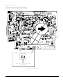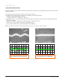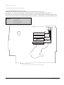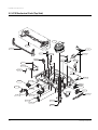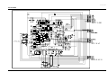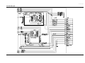
1
DVD-VCR COMBINATION Chassis : Kaiser DVD-V4300 DVD-V4600 SERVICE MANUAL SERVICE Manual DVD-V4300/V4600 If you want to know additional information which is not included on this Service Manual, please refer to the DVD-V4600 Training Manual (AK82-00460A). DVD-VCR COMBINATION CONTENTS 1. Precautions ELECTRONICS 2. Alignment and Adjustment 3. Exploded Views and Parts List 4. Electrical Parts List 5. Block Diagram 6. Schematic Diagrams DVD-V4300 DVD-V4600 This Service Manual is a property of Samsung Electronics Co .,Ltd. Any unauthorized use of Manual can be punished under applicable International and/or domestic law. © Samsung Electronics Co., Ltd. FEB. 2003 Printed in Korea AK82-00516A IMPORTANT SERVICE GUIDE ◆ MODE SWITCH (PROGRAM SWITCH) ASSEMBLY POINT 1) When installing the ass’y deck on the Main PCB, be sure to align the assembly point of mode switch. ASSEMBLY POINT VCR MAIN PCB Fig. 1 ◆ HOW TO EJECT THE CASSETTE TAPE (If the tape is stuck in the unit) 1) Turn the Gear Worm Œ clockwise in the direction of arrow with a screwdriver. (See Fig. 2) (Other method ; Remove the screw of Motor Load Ass’y, Separate the Motor Load Ass’y) 2) When Slider S, T approachs the unloading position, rotate holder Clutch counterclockwise after inserting screwdriver in the frame’s bottom hole in order to wind the unwound tape. (Refer to Fig. 3) (If you rotate Gear Worm Œ continuously when tape is unwinding, you may cause tape contamination by grease and tape damage. Be sure to wind the unwound tape with the unit in the horizontall position.) 3) Rotate Gear Worm Œ clockwise using a screwdriver until the mecha is in the eject state. Remove the tape. (Refer to Fig. 2) FRAME Œ GEAR WORM Fig. 2 Fig. 3 1. Precautions 1-1 Safety Precautions 1) Before returning an instrument to the customer, always make a safety check of the entire instrument, including, but not limited to, the following items: (1) Be sure that no built-in protective devices are defective or have been defeated during servicing. (1)Protective shields are provided to protect both the technician and the customer. Correctly replace all missing protective shields, including any removed for servicing convenience. (2)When reinstalling the chassis and/or other assembly in the cabinet, be sure to put back in place all protective devices, including, but not limited to, nonmetallic control knobs, insulating fish papers, adjustment and compartment covers/shields, and isolation resistor/capacitor networks. Do not operate this instrument or permit it to be operated without all protective devices correctly installed and functioning. (2) Be sure that there are no cabinet openings through which adults or children might be able to insert their fingers and contact a hazardous voltage. Such openings include, but are not limited to, excessively wide cabinet ventilation slots, and an improperly fitted and/or incorrectly secured cabinet back cover. (3) Leakage Current Hot Check-With the instrument completely reassembled, plug the AC line cord directly into a 120V AC outlet. (Do not use an isolation transformer during this test.) Use a leakage current tester or a metering system that complies with American National Standards institute (ANSI) C101.1 Leakage Current for Appliances and Underwriters Laboratories (UL) 1270 (40.7). With the instrument’s AC switch first in the ON position and then in the OFF position, measure from a known earth ground (metal water pipe, conduit, etc.) to all exposed metal parts of the instrument (antennas, handle brackets, metal cabinets, screwheads, metallic overlays, control shafts, etc.), especially any exposed metal parts that offer an electrical return path to the chassis. Any current measured must not exceed 0.5mA. Reverse the instrument power cord plug in the outlet and repeat the test. See Fig. 1-1. Any measurements not within the limits specified herein indicate a potential shock hazard that must be eliminated before returning the instrument to the customer. (READING SHOULD NOT BE ABOVE 0.5mA) LEAKAGE CURRENT TESTER DEVICE UNDER TEST TEST ALL EXPOSED METER SURFACES 2-WIRE CORD ALSO TEST WITH PLUG REVERSED (USING AC ADAPTER PLUG AS REQUIRED) EARTH GROUND Fig. 1-1 AC Leakage Test (4) Insulation Resistance Test Cold Check-(1) Unplug the power supply cord and connect a jumper wire between the two prongs of the plug. (2) Turn on the power switch of the instrument. (3) Measure the resistance with an ohmmeter between the jumpered AC plug and all exposed metallic cabinet parts on the instrument, such as screwheads, antenna, control shafts, handle brackets, etc. When an exposed metallic part has a return path to the chassis, the reading should be between 1 and 5.2 megohm. When there is no return path to the chassis, the reading must be infinite. If the reading is not within the limits specified, there is the possibility of a shock hazard, and the instrument must be repaired and rechecked before it is returned to the customer. See Fig. 1-2. Antenna Terminal Exposed Metal Part ohm ohmmeter Fig. 1-2 Insulation Resistance Test Samsung Electronics 1-1 Precautions 2) Read and comply with all caution and safety related notes on or inside the cabinet, or on the chassis. 3) Design Alteration Warning-Do not alter or add to the mechanical or electrical design of this instrument. Design alterations and additions, including but not limited to, circuit modifications and the addition of items such as auxiliary audio output connections, might alter the safety characteristics of this instrument and create a hazard to the user. Any design alterations or additions will make you, the servicer, responsible for personal injury or property damage resulting therefrom. 4) Observe original lead dress. Take extra care to assure correct lead dress in the following areas: (1) near sharp edges, (2) near thermally hot parts (be sure that leads and components do not touch thermally hot parts), (3) the AC supply, (4) high voltage, and (5) antenna wiring. Always inspect in all areas for pinched, out-of-place, or frayed wiring, Do not change spacing between a component and the printed-circuit board. Check the AC power cord for damage. 1-2 5) Components, parts, and/or wiring that appear to have overheated or that are otherwise damaged should be replaced with components, parts and/ or wiring that meet original specifications. Additionally, determine the cause of overheating and/or damage and, if necessary, take corrective action to remove any potential safety hazard. 6) Product Safety Notice-Some electrical and mechanical parts have special safety-related characteristics which are often not evident from visual inspection, nor can the protection they give necessarily be obtained by replacing them with components rated for higher voltage, wattage, etc. Parts that have special safety characteristics are identified by shading, an ( )or a ( )on schematics and parts lists. Use of a substitute replacement that does not have the same safety characteristics as the recommended replacement part might create shock, fire and/or other hazards. Product safety is under review continuously and new instructions are issued whenever appropriate. Samsung Electronics Precautions 1-2 Servicing Precautions CAUTION : Before servicing units covered by this service manual and its supplements, read and follow the Safety Precautions section of this manual. Note : If unforseen circumstances create conflict between the following servicing precautions and any of the safety precautions, always follow the safety precautions. Remember: Safety First. 1-2-1 General Servicing Precautions (1) a. Always unplug the instrument’s AC power cord from the AC power source before (1) re-moving or reinstalling any component, circuit board, module or any other instrument assembly, (2) disconnecting any instrument electrical plug or other electrical connection, (3) connecting a test substitute in parallel with an electrolytic capacitor in the instrument. b. Do not defeat any plug/socket B+ voltage interlocks with which instruments covered by this service manual might be equipped. c. Do not apply AC power to this instrument and /or any of its electrical assemblies unless all solid-state device heat sinks are correctly installed. d. Always connect a test instrument’s ground lead to the instrument chassis ground before connecting the test instrument positive lead. Always remove the test instrument ground lead last. (4) An insulation tube or tape is sometimes used and some components are raised above the printed wiring board for safety. The internal wiring is sometimes clamped to prevent contact with heating components. Install such elements as they were. (5) After servicing, always check that the removed screws, components, and wiring have been installed correctly and that the portion around the serviced part has not been damaged and so on. Further, check the insulation between the blades of the attachment plug and accessible conductive parts. 1-2-2 Insulation Checking Procedure Disconnect the attachment plug from the AC outlet and turn the power ON. Connect the insulation resistance meter (500V) to the blades of the attachment plug. The insulation resistance between each blade of the attachment plug and accessible conductive parts(see note) should be more than 1 Megohm. Note : Accessible conductive parts include metal panels, input terminals, earphone jacks, etc. Note : Refer to the Safety Precautions section ground lead last. (2) The service precautions are indicated or printed on the cabinet, chassis or components. When servicing, follow the printed or indicated service precautions and service materials. (3) The components used in the unit have a specified flame resistance and dielectric strength. When replacing components, use components which have the same ratings. Components identified by shading, by( ) or by ( ) in the circuit diagram are important for safety or for the characteristics of the unit. Always replace them with the exact replacement components. Samsung Electronics 1-3 Precautions 1-3 ESD Precautions Electrostatically Sensitive Devices (ESD) Some semiconductor (solid state) devices can be damaged easily by static electricity. Such components commonly are called Electrostatically Sensitive Devices(ESD). Examples of typical ESD devices are integrated circuits and some field-effect transistors and semiconductor chip components. The following techniques should be used to help reduce the incidence of component damage caused by static electricity. (1) Immediately before handling any semiconductor component or semiconductor-equipped assembly, drain off any electrostatic charge on your body by touching a known earth ground. Alternatively, obtain and wear a commercially available discharging wrist strap device, which should be removed for potential shock reasons prior to applying power to the unit under test. (7) Immediately before removing the protective materials from the leads of a replacement ESD device, touch the protective material to the chassis or circuit assembly into which the device will be installed. CAUTION : Be sure no power is applied to the chassis or circuit, and observe all other safety precautions. (8) Minimize bodily motions when handling unpackaged replacement ESD devices. (Otherwise harmless motion such as the brushing together of your clothes fabric or the lifting of your foot from a carpeted floor can generate static electricity sufficient to damage an ESD device). (2) After removing an electrical assembly equipped with ESD devices, place the assembly on a conductive surface such as aluminum foil, to prevent electrostatic charge buildup or exposure of the assembly. (3) Use only a grounded-tip soldering iron to solder or unsolder ESD devices. (4) Use only an anti-static solder removal devices. Some solder removal devices not classified as “anti-static” can generate electrical charges sufficient to damage ESD devices. (5) Do not use freon-propelled chemicals. These can generate electrical charges sufficient to damage ESD devices. (6) Do not remove a replacement ESD device from its protective package until immediately before your are ready to install it.(Most replacement ESD devices are packaged with leads electrically shorted together by conductive foam, aluminum foil or comparable conductive materials). 1-4 Samsung Electronics Precautions 1-4 Handling the optical pick-up The laser diode in the optical pick up may suffer electrostatic breakdown because of potential static electricity from clothing and your body. WRIST-STRAP FOR GROUNDING 1M The following method is recommended. (1) Place a conductive sheet on the work bench (The black sheet used for wrapping repair parts.) (2) Place the set on the conductive sheet so that the chassis is grounded to the sheet. (3) Place your hands on the conductive sheet(This gives them the same ground as the sheet.) (4) Remove the optical pick up block (5) Perform work on top of the conductive sheet. Be careful not to let your clothes or any other static sources to touch the unit. THE UNIT 1M CONDUCTIVE SHEET Fig.1-3 (6) Short the short terminal on the PCB, which is inside the Pick-Up ASS’Y, before replacing the PickUp. (The short terminal is shorted when the PickUp Ass’y is being lifted or moved.) (7) After replacing the Pick-up, open the short terminal on the PCB. ◆ Be sure to put on a wrist strap grounded to the sheet. ◆ Be sure to lay a conductive sheet made of copper etc. Which is grounded to the table. Samsung Electronics 1-5 Precautions 1-5 Pick-up disassembly and reassembly 1-5-1 Disassembly 1-5-2 Assembly 1) Remove the power cord. 2) Disassemble the Deck-Assy. 3) Make solder land 2 points short on Pick-up. (See Fig. 1-4) 4) Disassemble the Pick-up. 1) Replace the Pick-up. 2) Remove the soldering 2 points on Pick-up. 3) Reassemble the Deck-Assy. Note : If the assembly and disassembly are not done in correct sequence, the Pick-up may be damaged. SOLDER LAND 2 POINTS SHORT PICK-UP ASS'Y Fig. 1-4 1-6 Samsung Electronics 2. Alignment and Adjustments 2-1 VCR Adjustment 2-1-1 Reference 1) X-Point (Tracking center) adjustment, “Head switching adjustment” and “NVRAM option setting” can be adjusted with remote control. 2) When replacing the Main PCB Micom (IC601) and NVRAM (IC603 ; EEPROM) be sure to adjust the “Head switching adjustment” and “NVRAM option setting”. 3) When replacing the cylinder ass’y, be sure to adjust the “X-Point” and “Head switching adjustment”. 4) How to adjust. - Intermittently short-circuit the Test Point on Main PCB with pincers to the adjustment mode. - If the corresponding adjustment button is pressed, the adjustment is performed automatically. - When the adjustment is completed, be sure to turn the power off. 2-1-1(a) Location of adjustment button of remote control X-Point (Tracking Center) Adjustment ; NVRAM Option Setting ; Head Switching Adjustment ; Fig. 2-1 Samsung Electronics 2-1 Alignment and Adjustments 2-1-1(b) TEST location for adjustment mode setting Short-Circuit for few seconds and release. (Just one time) Fig. 2-2 VCR Main PCB (Top View) 2-2 Samsung Electronics Alignment and Adjustments 2-1-2 Head Switching Point Adjustment 1) Playback the alignment tape. 2) Intermittently short-circuit the two Test Points on VCR Main PCB while setting the adjustment mode. (See Fig. 2-2) 3) Press the “1, 0” buttons; remote control adjustment operates automatically. (See Fig. 2-1) 2-1-3 NVRAM Option Setting 1) NVRAM Option is adjusted in the factory. 2) In case Main PCB Micom (IC601) and NVRAM (IC603 ; EEPROM) are replaced, be sure to set the corresponding option number of the required model. (If the option is not set, the unit will not operate.) 1) Intermittently short-circuit the two Test Points on VCR Main PCB. (See Fig. 2-2) 2) Press the “1, 4” button on the remote control. The option setting appears. (See Fig. 2-3) 3) Select the option number (See table 2-1) of corresponding model with “ , , , ” buttons on the remote control. 4) After selecting the option number is completed, press the “ ” button of remote control. (If “ ” button is pressed, the selected number is changescolor. ; See Fig. 2-4) 5) Press the “ENTER” button of remote control again to store the option number. 6) Turn the Power off. 01 02 03 04 05 06 07 08 01 02 03 04 05 06 07 08 09 10 11 12 13 14 15 16 09 10 11 12 13 14 15 16 17 18 19 20 21 22 23 24 17 18 19 20 21 22 23 24 25 26 27 28 29 30 31 32 25 26 27 28 29 30 31 32 33 34 35 36 37 38 39 40 33 34 35 36 37 38 39 40 MOVE : SAVE : ENTER Fig. 2-3 MOVE : COMPLETE Fig. 2-4 <Table 2-1 NVRAM Option Table> MODEL DVD-V4300 DVD-V4600 Samsung Electronics OPTION NUMBERS 2, 7, 8, 9, 14, 16, 18, 22, 25, 28 2, 7, 8, 9, 14, 16, 18, 22, 25, 28 2-3 Alignment and Adjustments 2-2 DVD Adjustment 2-2-1 Location of Test Point S Fig. 2-5 Location of test Point (Main PCB - Top Side) 2-4 Samsung Electronics Alignment and Adjustments 2-2-2 Skew Adjustment 2-2-2(a) Adjustment Spec. and Test Point ◆ Test Disc ; Service not Available <Table 2-2> Test Disc Adjustment Spec. Test Point Adjustment Location TDV-533 Chapter 14 Flat Waveform “ENV” (DVD Main PCB - Top Side) (See Fig. 2-5) Ass’y Deck - Top Side (See Fig. 2-6) Fig. 2-6 Ass’y Deck (Top Side) Samsung Electronics 2-5 Alignment and Adjustments 2-2-2(b) SKEW Adjustment Method Needed to minimize the variations in Skew of the Pickup unit and to provide optimum match with the recorded signal on the Disc. 1) Connect an Oscilloscope to the “ENV” Test Point (See Fig. 2-5). 2) Connect Power, Open the Tray and Play Ch.14 Which is in the TDV-533 Disc. ◆ Set the Oscilloscope Range as follows : (Voltage ; 50mV/Div., Frequency ; 10m Sec.) 3) Adjust the Screws “A” and “B” (See Fig. 2-6) using a Hex screwdriver until you obtain a Flat Waveform and the picture is stable. Then, go to Chapter 1 and make sure the Waveform is Flat here as well. If not, you have to go back to Chapter 14 and adjust again. If you cannot obtain a Flat waveform, then the unit is defective. Note : The Deck must be in a horizontal position. Use both “A” and “B” screws to adjust. Typical Waveform before Adjustment Waveform after Correct Adjustment Fig. 2-7 Envelope Waveform 2-6 Samsung Electronics Alignment and Adjustments 2-3 VCR Mechanical Adjustment 2-3-1 Tape Transport System and Adjustment Locations The tape transport system has been adjusted precisely in the factory. Alignment is not necessary except for the following : 1) Noise observed on the screen. 2) Tape damage. 3) Parts replacement in the tape transport system. Lower flange height of tape guide is used as the reference for the transport adjustment. To maintain the height of the tape guide and prevent damage, do not apply excessive force onto the main base. CYLINDER ASS'Y GUIDE ROLLER "S" GUIDE ROLLER "T" FULL ERASE HEAD HEIGHT SCREW #3 GUIDE POST TENSION POST PINCH ROLLER TILT SCREW X - POSITION ADJUST SILT #9 GUIDE POST AZIMUTH SCREW CAPSTAN #8 GUIDE POST TAKE UP REEL DISK SUPPLY REEL DISK Fig. 2-8 Location of Tape Transport Adjustment PINCH ROLLER FE HEAD CYLINDER ASS'Y GUIDE ROLLER "S" GUIDE ROLLER "T" POST TENSION #8 GUIDE POST #9 GUIDE POST #3 GUIDE POST MAIN BASE ACE HEAD CAPSTAN SHAFT Fig. 2-9 Tape Travel Diagram Samsung Electronics 2-7 Alignment and Adjustments 2-3-2 Tape Transport System Adjustment When parts are replaced, perform the required adjustments by referring to procedures for the tape transport system. If there are any changes to the tape path, first run a T-120 tape and make sure excessive tape wrinkle does not occur at the tape guides. ◆ If tape wrinkle is observed at the guide roller S, T, turn the guide roller S, T until wrinkle disappears. ◆ If the tape wrinkle is still observed at the tape guide, perform the tilt adjustment of the ACE head. (1) ACE Head Assembly Adjustment a. ACE HEAD HEIGHT ADJUSTMENT 1) Run the alignment tape (Color bar) in the playback mode. 2) Observe surface of the audio head using a dental mirror. 3) Turn screw (C) clockwise or counterclockwise until the gap of lower tape edge and the lower edge of the control head is about 0.25mm. (Refer to Fig. 2-10 and 2-11) SCREW (A) TLIT ADJUST SCREW (C) HEIGHT ADJUST X-POSITION ADJUSTING SLIT SCREW (D) X-POSITION LOCKING SCREW (B) AZIMUTH ADJUST Fig. 2-10 Location of ACE Head Adjustment Screw AUDIO HEAD VIDEO HEAD 0 ~ 0 .25 mm CONTROL HEAD Fig. 2-11 ACE Head Height Adjustment 2-8 Samsung Electronics Alignment and Adjustments b. ACE HEAD TILT ADJUSTMENT 1) Playback a blank tape and observe the position of the tape at the lower flange of tape guide. 2) Confirm that there is no curl or wrinkle at the lower flange of tape guide as shown in Fig. 2-12 (B). 3) If a curl or wrinkle of the tape occurs, slightly turn the screw (A) tilt adjust on the ACE head ass’y. 4) Reconfirm the ACE head height. (A) (B) (BAD) (GOOD) WRINKLE Fig. 2-12 Tape Guide Check c. AUDIO AZIMUTH ADJUSTMENT 1) Load alignment tape (Mono scope) and playback the 7KHz signal. 2) Connect channel-1 scope probe to audio output. 3) Adjust screw (B) to achieve maximum audio level. (See Fig. 2-10) Samsung Electronics 2-9 Alignment and Adjustments d. ACE HEAD POSITION (X-POINT) ADJUSTMENT 1) Playback the alignment tape (Color bar) 2) Intermittently short-circuit the two Test Points on VCR Main PCB. (See Fig. 2-2) 3) Press the “0, 5” remote control buttons, then adjustment is operates automatically. (See Fig. 2-1) 4) Connect the CH-1 probe to “Envelope” the CH-2 probe to “H’D switching pulse” and then trigger to CH-1. 5) Insert the (-) driver into the X-Point adjustment hole and adjust it so that envelope waveform is maximum. Test point : TP2 (Audio Output) TP3 (Envelope) TP4 (H’D S/W -Trigger) TP5 (Control Pulse) CONTROL PULSE HEAD SWITCHING ENVELOPE AUDIO OUTPUT Fig. 2-13 Location of Test point (VCR Main PCB-Top View) 2-10 Samsung Electronics Alignment and Adjustments (2) Linearity adjustment (Guide roller S, T adjustment) 1) Playback the Mono Scope alignment tape (SP mode). 2) Observe the video envelope signal on an oscilloscope (triggered by the video switching pulse). 3) Make sure the video envelope waveform (at its minimum) meets the specification shown in Fig. 2-14. If it does not, adjust as follows : Note : a=Maximum output of the video RF envelope. b=Minimum output of the video RF envelope at the entrance side. c=Minimum output of the video RF envelope at the center point. d=Maximum output of the video RF envelope at the exit side. 4) If the section A in Fig. 2-15 does not meet the specification, adjust the guide roller S up or down. 5) If the section B in Fig. 2-15 does not meet the specification, adjust the guide roller T up or down. c a b d abcd 63% c,b,d/a Fig. 2-14 Envelope Waveform Adjustment H'D SWITCHING PULSE A ENVELOPE A B B Fig. 2-15 Adjustment Points Samsung Electronics 2-11 Alignment and Adjustments 6) Play back the Mono Scope alignment tape (SP mode). 7) Connect an oscilloscope CH-1 to the “Envelope” and CH-2 to the “H’D SW Pulse” for triggering. 8) Turn the guide roller heads with a flat head ( ) driver to obtain a flat video RF envelope as shown in Fig. 2-16. IDEAL ENVELOPE S HEIGHT TOO HIGH S HEIGHT TOO LOW T HEIGHT TOO HIGH GUIDE ROLLER S T HEIGHT TOO LOW GUIDE ROLLER T Fig. 2-16 Guide Roller S, T Height Adjustment 2-12 Samsung Electronics Alignment and Adjustments (3) Check Transitional Operation from RPS to Play Check transition from RPS mode to play mode : Using a pre-recorded SP tape, make sure the entry side of envelope comes to an appropriate steady state within 3 seconds (as shown in Fig. 2-17). If the envelope waveform does not reach specified peak-to peak amplitude within 3 seconds, adjust as follows : 1) Make sure there is no gap between the supply roller lower flange and the tape. If there is a gap, adjust the supply guide roller again. 2) Change operation mode from the RPS to the play mode (again) and make sure the entry side of envelope rises within 3 seconds. ENTRANCE SIDE ENVELOPE Fig. 2-17 Video Envelope Rising when Operation mode Changes from RPS to Play Mode (4) Envelope Check 1) Make recordings on T-120 (E-120) and T-160 (E-180) tape. Make sure the playback output envelope meets the specification as shown in Fig. 2-18. 2) Play back a self recorded tape (recording made on the unit using with T-120 (E-120). The video envelope should meet the specification as shown in Fig. 2-18. In SP mode, (A) should equal (B). If the head gap is wide, upper cylinder should be checked. A B Fig. 2-18 Envelope Input and Output Level (5) Tape Wrinkle Check 1) Run the T-160 (E-180) tape in the playback, FPS, RPS and Pause modes and observe tape wrinkle at each guide. 2) If excessive tape wrinkle is observed, perform the following adjustments in Playback mode : ◆ Tape wrinkle at the guide roller S, T section : Linearity adjustment. ◆ Tape wrinkle at tape guide flange : ACE head assembly coarse adjustment. Samsung Electronics 2-13 Alignment and Adjustments 2-3-3 Reel Torque 1) The rotation of the capstan motor causes the holder clutch ass’y to rotate through the belt pulley. 2) The spring wrap PLAY/REV of holder clutch ass’y drives the disk reel S, T through gear idler by rotation of gear center ass’y. 3) Brake is operated by slider cam at FF/REW mode. 4) Transportation of accurate driving force is done by gears. (Gear Center Ass’y) Note : If the spec. does not meet the followings specifications, replace the holder clutch ass’y and then recheck. <Table 2-4> MODE TORQUE g/cm GAUGE PB 42 ± 11 Cassette Torquemeter RPS 145 ± 30 Cassette Torquemeter 2-14 Samsung Electronics 3. Exploded View and Parts List 3-1 Cabinet Assembly - - - - - - - - - - - - - - - - - - - - - - - - - - - - - - - - - - - - - - - - - 3-2 3-2 VCR Mechanical Parts (Top Side) - - - - - - - - - - - - - - - - - - - - - - - - - - - - - - 3-4 3-3 VCR Mechanical Parts (Bottom Side) - - - - - - - - - - - - - - - - - - - - - - - - - - - - 3-6 3-4 DVD Mechanical Parts - - - - - - - - - - - - - - - - - - - - - - - - - - - - - - - - - - - - - 3-8 Notice You can search for the updated part code through ITSELF web site. URL; http://itself.sec.samsung.co.kr Samsung Electronics 3-1 3-2 VCR DECK (S.N.A.) DVD DECK (S.N.A.) 157 157 2 153 3 BRACKET-FRAME (S.N.A.) 21 701 (FUNCTION PCB) LD601A 602 (DVD MAIN PCB) S602A 22 1 603 (S.M.P.S. PCB) 200 ASSY FRAME (S.N.A) 101 S.N.A. : Service Not Available 601 (VCR MAIN PCB) TM401B UT01 155 Exploded View and Parts List 3-1 Cabinet Assembly Samsung Electronics Exploded View and Parts List Loc. No 1 2 3 21 22 101 153 155 157 200 601 602 603 701 LD601A S602A TM401B UT01 Parts No. AK97-00883B AK97-00717L AK64-00628A AK64-00557A AK64-00334A AK64-00627B AK64-00556H AC61-62032A AK64-00535A AC60-12126A 6003-000275 AC60-10063A AC39-10014A AC39-00019A AK92-00387D AK92-00341A AK94-00006B AK94-00011A AK94-00010A AC61-00340A AC61-00341A AK97-00749B AK59-00008A Samsung Electronics Description ; Specification ASSY-PANEL FRONT;ASS,DVD-V4300/XAX,04-C ASSY-PANEL FRONT;HIPS 94HB,DVD-V4600/XAP DOOR-TRAY;DVD-V340,ABS,T2,H17.8,W130.8,DOOR-TRAY;DVD-V4500/XAA,ABS 94HB,T2.0,H1 DOOR-SPRING;DVD-V3500,SWPB,,,,-,, DOOR-CASSETTE;DVD-V4300/XAX,ABS 94,T2.2, DOOR-CASSETTE;DVD-V4600/XAP,ABS,-,-,W26, SPRING ETC-MASK;SV-C130,SUS,4.4,-,-,-,-, CABINET-TOP;DVD-V4500,PCM,T0.5,W430,L223 SCREW-BH;-,-,FE,FZY,BH,-,-,4*12,-,SCREW-TAPTITE;BH,+,B,M3,L10,BLK ,SWCH101 SCREW-TAPTITE;-,-,L12,ZPC3,+,-,M3,-,SWRC CBF POWER CORD;KKP-211,VFF0.75MM,JIS,CON CBF POWER CORD;KKP-419C,H03VVH2-F,VDE/KE ASSY PCB-MAIN VCR;DVD-V4300/XAX,LED-M ASSY PCB-MAIN DVD;DVD-V4500,VENUS,SEA ASSY PCB-SMPS;DVD-V4300/XAX,FREE ASSY SORT-FUNCTION;DVD-V4700,04-SECCOM43 ASSY SORT-FUNCTION;DVD-V4600,04-SECCOM43 HOLDER-LED;X-11,POM(K300),-,-,-,NTR,HOLDER-TR;X-11,POM(K300),-,-,-,NTR,ASSY-CON BOARD;HIPS 94HB,DVD-V4800,DVD-V REMOCON-ASSY;DVD-V3000/XAA,SAMSUNG,-,-,4 Remark DVD-V4300 Only DVD-V4600 Only DVD-V4300 Only DVD-V4600 Only DVD-V4300 Only DVD-V4600 Only Other Only CHILE/PERU Only DVD-V4300 Only DVD-V4600 Only 3-3 Exploded View and Parts List 3-2 VCR Mechanical Parts (Top Side) G001 K490 K502 K530 G530 G555 B474 G450 G510 G420 B473 G480 K546 K250 K240 K248 B411 B410 K350 K110 B440 K182 B448 K340 K330 B452 G546 K470 K140 K188 G527 G070 G520 G060 3-4 Samsung Electronics Exploded View and Parts List Loc. No B410 B411 B440 B448 B452 B473 B474 G001 G060 G070 G420 G450 G480 G510 G520 G527 G530 G546 G555 G560 K110 K140 K182 K188 K240 K248 K250 K330 K340 K350 K470 K490 K502 K530 K546 Parts No. AC97-02354A AC71-00004A AC60-10515A AC66-00008A AC66-00011A AC61-00105A AC61-30180A AC97-02191A 6006-001092 AC70-00002A AC66-80142A AC66-80141A AC97-01660A 6006-001075 AC66-00074A AC61-60553A AC33-00007A AC66-00005A AC97-02293A AC97-02215A AC66-10267A AC66-10268A AC66-30524A AC66-00039A AC66-00035A AC61-00107A AC69-00104A AC66-30550A AC66-30549A AC61-00106A AC66-00020A AC61-00120A AC61-60561A AC66-00034A AC61-50658A Samsung Electronics Description ; Specification Remark ASSY-LOADING MOTOR;ASSY-LOADING MOTOR, WIRE-LOADING;X-11,PVC+ WIRE,T0.38,0.88, SCREW-MACHINE;-,-,M3,L3,PH,+,-,-,ZPC,GEAR-WORM WHEEL;TS-10,POM,0.8,40,-,NAT,3 GEAR-FL CAM;TS-10,POM,0.8,59,-,BLK,48.48 SPRING ETC-PINCH DRIVE;TS-10,SUS304-WPB, PLATE-JOINT;X-9,SECC20/20,T0.8,-,-,-,ASSY-CYLINDER;6ANJ(Alps Head),CX11-DS,Fo SCREW-ASS’Y MACH;WS,PH,+,M3.0,L6.0,ZPC(Y PLATE-GND DECK;X-11,SPTE,T0.3,-,-,-,SLIDER-SUPPLY ASSY;X-9,SUS,-,-,-,SIL,SLIDER-TAKE UP ASSY;X-9,SUS,-,-,-,SIL,ASSY-HEAD ACE;-,SCORPIO2(TS-10A),VTR-1*2 SCREW-ASS’Y TAPT;WSP,PH,+,M2.6,L5.0,ZPC( LEVER-GUIDE(#9);TS-9,PPS,-,-,-,-,BLK,KHA SPRING ETC-GUIDE 9;X-9,SUS304-WPB,0.25,HEAD-FE;-,-,HVFHPOO43A,-,LEVER-FL DOOR;TS-10,POM,-,-,-,-,NAT,ASSY-UNIT PINCH;SECC+SUS304,TS-10,FOR XASSY-POST #8 GUIDE;SUS303+POM(M90-44)EQ, REEL-DISK S;X-9,POM,-,-,-,-,-,REEL-DISK T;X-9,POM,-,-,-,-,-,LEVER-IDLER;-,POM,-,-,-,-,BLK,GEAR-IDLE;TS-10,PET K3372,0.5,-,-,NTR,28 LEVER-TENSION ASS’Y;TS-10,SECC E20/20+SU SPRING ETC-TENSION LEVER;TS-10,SUS304-WP BAND-BRAKE ASS’Y;TS-10,-,-,-,-,-,LEVER-S.BRAKE ASSY;-,POM+SUS,-,-,-,X-9 LEVER-T.BRAKE ASSY;-,POM+SUS,-,-,-,X-9 SPRING ETC-BRAKE;TS-10,SUS304-WPB,-,-,-, SLIDER-FL DRIVE;TS-10,SECC ,T1.0,-,-,SIL HOLDER-FL CASS. ASS’Y;TS-10,-,-,-,-,-,SPRING ETC-FL.LEVER-LR;X-9,SUS304 WPB,OD LEVER-FL ARM ASS’Y;TS-10,-,-,-,-,-,-,GUIDE-CASS. DOOR;X-9,POM,-,-,-,NTR 3-5 Exploded View and Parts List 3-3 VCR Mechanical Parts (Bottom Side) G542 B462 B456 B460 B560 B500 B458 B464 B488 B484 B468 B475 K222 K200 K225 K221 B478 B570 3-6 Samsung Electronics Exploded View and Parts List Loc. No B456 B458 B460 B462 B464 B468 B475 B478 B484 B488 B500 B560 B570 G542 K200 K221 K222 K225 Parts No. AC66-00076A AC66-00077A AC61-00338A AC60-10517A AC66-00075A AC66-00017A AC66-00085A AC66-00016A AC66-00078A AC97-02195A AC97-02196A AC81-00004A AC60-10514A AC66-60051A AC61-21012A AC66-20581A AC60-30306A AC66-00006A Samsung Electronics Description ; Specification Remark GEAR-JOINT 1;X-11,POM(K300),-,-,-,BLUE,GEAR-JOINT 2;X-11,POM(K300),-,-,-,BLUE,BRACKET-GEAR;X-11,SECC,T0.8,W20,L20,NTR, SCREW-TAP TITE;-,-,M2.6,L5,PH,+,-,-,ZPC, SLIDER-CAM;X-11,SECC ,T1.2,-,-,SIL,LEVER-PINCH DRIVE;TS-10,SECC E20/20,1.0 DAMPER-CAPSTAN;X-11,POM(M90-44),-,-,-,-, LEVER-TENSION DRIVE;TS-10,SECC E20/20,1 GEAR-LOADING DRIVE;X-11,POM(K300),-,-,-, ASSY-LEVER LOADING S;SECC+POM+SUS,X-11,F ASSY-LEVER LOADING T;SECC+POM+SUS,X-11,F MOTOR-CAPSTAN;THRUST END PLAY-0.2,MR-FG SCREW-CAPSTAN;-,-,M2.6,L6,PH,+,-,-,-,BELT-PULLEY;-,5CM-70,2 * 2,-,71.3,-,X-9 HOLDER-CLUTCH ASSY;X-9,ABS,-,-,-,BLK,GEAR-CENTER ASSY;X-9,POM,M=O.5,-,-,GRY,FASTENER-WASHER SLIT;-,-,ID2.1,OD5.0,T0. LEVER-UP DOWN;TS-10,POM,-,-,-,-,NAT,- 3-7 Exploded View and Parts List 3-4 DVD Mechanical Parts H212 H102 H205 H900 H204 H202 H903 H903 H210 H211 H207 H241 H206 H206 H904 H904 H203 H209 H107 H105 H106 H103 H903 H108 H104 H109 3-8 Samsung Electronics Exploded View and Parts List Loc. No H102 H103 H104 H105 H106 H107 H108 H109 H202 H203 H204 H205 H206 H207 H209 H210 H211 H212 H241 H900 H903 H904 Parts No. AH66-00111B AK66-00042A AK97-00608A 6602-001076 AK66-00041A AK66-00045A AK63-00101B AK92-00328B AK73-00005B AH61-50327A AK66-00043A AK66-00044A AK61-00032A AK31-00014A AK64-00491A AK31-00005A AK97-00638A AK61-00253A AK41-00156B 6003-001157 6001-001370 6002-001086 Samsung Electronics Description ; Specification Remark CLAMPER-ASSY;DP-5,POM,-,-,-,-,BLK,GEAR-PULLEY;DP-15,POM,-,-,-,WHT,-,-,ASSY-MOTOR LOAD;-,DP-15,BELT-RECTANGULAR;CR,T1.2,4.3%,1.2X25.1,B GEAR-TRAY;DP-15,POM,-,-,-,WHT,-,-,SLIDER HOUSING;DP-15,POM,-,W17.8,L90,WHT TRAY-DISC;DP-15,ABS,-,W120,L186.3,-,GRY, ASSY PCB-DECK;DP-15,COMBO RUBBER-INSULATOR;DP-15,BUTYL,•’12,HS30,H SHAFT-P/U;DP-3,SUS,L84.7,OD3,-,-,GEAR-FEED A;DP-15,POM,-,-,-,-,-,-,GEAR-FEED B;DP-15,POM,-,-,-,-,-,-,HOLDER-CAM SKEW;DP-9,POM,-,-,-,BLACK,MOTOR SPINDLE;DP-15,3000RPM,-,-,-,CHASSIS SUB;DP-15,POM,-,-,-,-,MOTOR-FEED ASSY;-,DP-9,-,-,-,-,-,-,-,-,ASSY-PICK UP;-,SOH-DT2,TRINO ASSY PICK U HOLDER-CHUCK;DP-15,POM,-,-,-,-,FFC-PU;DP-15,-,FFC,24,T0.3,RIGHT SCREW-TAPTITE;PWH,+,B,M2,L6,ZPC(YEL),SWR SCREW-MACHINE;CH,+,M1.7,L3.0,ZPC(YEL),SW SCREW-TAPPING;PH,+,B,M1.7,L5.0,ZPC(YEL), 3-9 Exploded View and Parts List MEMO 3-10 Samsung Electronics 4. Electrical Parts List Loc.No 601 AC14 AC21 AC22 AC23 AC24 AC25 AC26 AC27 AC9 AD1 AD2 AE11 AE12 AE13 AE14 AE3 AE5 AIC4 AQ1 AQ2 AQ3 AQ4 AQ5 AQ6 AR14 AR15 AR16 AR17 AR28 AR29 AR30 AR31 AR41 AR42 AR43 AR44 AR45 AR46 AR47 AR48 AR49 AR50 C1P102 C1P111 C1P112 C1P114 C1P116 C1P117 C1P118 C301 C302 C303 C304 C305 C306 C307 C308 C309 C310 C311 Part No AK92-00387D 2203-001607 2203-000315 2202-002037 2203-000125 2203-005148 2203-000315 2203-000125 2203-005148 2203-001607 0407-000114 0407-000114 2401-000918 2401-003107 2401-000918 2401-003107 2401-000918 2401-000918 1201-000163 0504-000128 0504-000156 0501-000341 0504-000128 0504-000156 0501-000341 2007-000090 2007-000074 2001-000281 2001-000429 2007-000090 2007-000074 2001-000281 2001-000429 2007-001179 2007-000078 2007-000092 2007-000097 2007-000097 2007-001179 2007-000078 2007-000092 2001-000786 2007-000097 2401-001479 2401-000414 2401-001250 2401-001730 2401-003107 2203-000257 2401-002075 2203-005065 2203-006243 2203-005065 2203-000405 2203-005065 2203-005148 2401-001502 2401-000909 2401-000408 2203-005065 2401-000408 Samsung Electronics Description ; Specification ASSY PCB-MAIN VCR;DVD-V4300/XAX,LED-M C-CER,CHIP;0.22nF,5%,50V,NP0,-,1608 C-CER,CHIP;0.12NF,5%,50V,C0G,TP,1608 C-CERAMIC,MLC-AXIAL;100nF,80-20%,50V,Y5V C-CER,CHIP;1.2nF,10%,50V,X7R,TP,1608,C-CER,CHIP;100nF,10%,16V,X7R,TP,1608 C-CER,CHIP;0.12NF,5%,50V,C0G,TP,1608 C-CER,CHIP;1.2nF,10%,50V,X7R,TP,1608,C-CER,CHIP;100nF,10%,16V,X7R,TP,1608 C-CER,CHIP;0.22nF,5%,50V,NP0,-,1608 DIODE-ARRAY;DAN202K,80V,100mA,CA2-3,SOTDIODE-ARRAY;DAN202K,80V,100mA,CA2-3,SOTC-AL;22uF,20%,16V,GP,-,6.3x7,5 C-AL;47uF,20%,16V,GP,TP,5x7,5 C-AL;22uF,20%,16V,GP,-,6.3x7,5 C-AL;47uF,20%,16V,GP,TP,5x7,5 C-AL;22uF,20%,16V,GP,-,6.3x7,5 C-AL;22uF,20%,16V,GP,-,6.3x7,5 IC-OP AMP;4560,SOP,8P,173MIL,DUAL,100V/m TR-DIGITAL;-,NPN,200MW,22K/22K,SOT-23,TP TR-DIGITAL;KSR2103,PNP,200MW,22K/22K,SOT TR-SMALL SIGNAL;KSC1623-L,NPN,200mW,SOTTR-DIGITAL;-,NPN,200MW,22K/22K,SOT-23,TP TR-DIGITAL;KSR2103,PNP,200MW,22K/22K,SOT TR-SMALL SIGNAL;KSC1623-L,NPN,200mW,SOTR-CHIP;10Kohm,5%,1/10W,TP,1608 R-CHIP;100ohm,5%,1/10W,TP,1608 R-CARBON;100OHM,5%,1/8W,AA,TP,1.8X3.2MM R-CARBON;1KOHM,5%,1/8W,AA,TP,1.8X3.2MM R-CHIP;10Kohm,5%,1/10W,TP,1608 R-CHIP;100ohm,5%,1/10W,TP,1608 R-CARBON;100OHM,5%,1/8W,AA,TP,1.8X3.2MM R-CARBON;1KOHM,5%,1/8W,AA,TP,1.8X3.2MM R-CHIP;8.2Kohm,5%,1/10W,TP,1608 R-CHIP;1Kohm,5%,1/10W,TP,1608 R-CHIP;15Kohm,5%,1/10W,TP,1608 R-CHIP;47Kohm,5%,1/10W,TP,1608 R-CHIP;47Kohm,5%,1/10W,TP,1608 R-CHIP;8.2Kohm,5%,1/10W,TP,1608 R-CHIP;1Kohm,5%,1/10W,TP,1608 R-CHIP;15Kohm,5%,1/10W,TP,1608 R-CARBON;47KOHM,5%,1/8W,AA,TP,1.8X3.2MM R-CHIP;47Kohm,5%,1/10W,TP,1608 C-AL;470UF,20%,10V,GP,TP,6.3*11MM,C-AL;10uF,20%,16V,GP,TP,4x7,5 C-AL;4.7uF,20%,35V,GP,TP,4x5,5 C-AL;10UF,20%,50V,GP,TP,5X11,5 C-AL;47uF,20%,16V,GP,TP,5x7,5 C-CER,CHIP;10nF,10%,50V,X7R,TP,1608 C-AL;4.7uF,20%,50V,GP,TP,5x11,5 C-CER,CHIP;1000nF,+80-20%,10V,Y5V,-,1608 C-CER,CHIP;0.36NF,10%,50V,X7R,TP,1608 C-CER,CHIP;1000nF,+80-20%,10V,Y5V,-,1608 C-CER,CHIP;0.18NF,5%,50V,C0G,TP,1608 C-CER,CHIP;1000nF,+80-20%,10V,Y5V,-,1608 C-CER,CHIP;100nF,10%,16V,X7R,TP,1608 C-AL;47uF,20%,16V,GP,TP,6.3x5,2.5 C-AL;22uF,20%,16V,GP,TP,5x5,2.5 C-AL;10uF,20%,16V,GP,TP,3.5x5,2.5 C-CER,CHIP;1000nF,+80-20%,10V,Y5V,-,1608 C-AL;10uF,20%,16V,GP,TP,3.5x5,2.5 Remark Loc.No C312 C313 C314 C315 C316 C317 C318 C319 C320 C321 C322 C323 C324 C325 C326 C327 C328 C329 C330 C331 C332 C333 C334 C335 C336 C337 C338 C340 C342 C343 C344 C345 C346 C347 C348 C349 C350 C351 C352 C353 C354 C355 C356 C357 C358 C359 C360 C371 C372 C401 C402 C403 C405 C406 C407 C408 C501 C502 C503 C504 C505 Part No 2203-000257 2401-000408 2203-005065 2203-005065 2203-005065 2203-005065 2202-000797 2202-000797 2203-000257 2401-001502 2203-005148 2203-005065 2203-000257 2203-005065 2203-002398 2203-005065 2401-001502 2203-000257 2203-000975 2203-000975 2203-000975 2203-000975 2401-001502 2203-005148 2203-005065 2401-001502 2203-000257 2401-000918 2401-001169 2203-005148 2203-001587 2203-000257 2401-000414 2203-000491 2203-001052 2401-001250 2203-001103 2203-001211 2203-000257 2401-001250 2203-002041 2301-000110 2401-001502 2301-000174 2203-000257 2203-000257 2203-000257 2203-001071 2203-005148 2203-005148 2203-005148 2203-005148 2401-001479 2203-000257 2203-002398 2401-001730 2203-001724 2202-002037 2401-000408 2203-005065 2401-000909 Description ; Specification Remark C-CER,CHIP;10nF,10%,50V,X7R,TP,1608 C-AL;10uF,20%,16V,GP,TP,3.5x5,2.5 C-CER,CHIP;1000nF,+80-20%,10V,Y5V,-,1608 C-CER,CHIP;1000nF,+80-20%,10V,Y5V,-,1608 C-CER,CHIP;1000nF,+80-20%,10V,Y5V,-,1608 C-CER,CHIP;1000nF,+80-20%,10V,Y5V,-,1608 C-CERAMIC,MLC-AXIAL;10NF,30%,16V,Y5S,TP, C-CERAMIC,MLC-AXIAL;10NF,30%,16V,Y5S,TP, C-CER,CHIP;10nF,10%,50V,X7R,TP,1608 C-AL;47uF,20%,16V,GP,TP,6.3x5,2.5 C-CER,CHIP;100nF,10%,16V,X7R,TP,1608 C-CER,CHIP;1000nF,+80-20%,10V,Y5V,-,1608 C-CER,CHIP;10nF,10%,50V,X7R,TP,1608 C-CER,CHIP;1000nF,+80-20%,10V,Y5V,-,1608 C-CER,CHIP;22nF,10%,50V,X7R,TP,1608 C-CER,CHIP;1000nF,+80-20%,10V,Y5V,-,1608 C-AL;47uF,20%,16V,GP,TP,6.3x5,2.5 C-CER,CHIP;10nF,10%,50V,X7R,TP,1608 C-CER,CHIP;47nF,10%,25V,X7R,TP,1608,C-CER,CHIP;47nF,10%,25V,X7R,TP,1608,C-CER,CHIP;47nF,10%,25V,X7R,TP,1608,C-CER,CHIP;47nF,10%,25V,X7R,TP,1608,C-AL;47uF,20%,16V,GP,TP,6.3x5,2.5 C-CER,CHIP;100nF,10%,16V,X7R,TP,1608 C-CER,CHIP;1000nF,+80-20%,10V,Y5V,-,1608 C-AL;47uF,20%,16V,GP,TP,6.3x5,2.5 C-CER,CHIP;10nF,10%,50V,X7R,TP,1608 C-AL;22uF,20%,16V,GP,-,6.3x7,5 C-AL;33UF,20%,16V,GP,-,6.3X7,5 C-CER,CHIP;100nF,10%,16V,X7R,TP,1608 C-CER,CHIP;18nF,10%,50V,X7R,TP,1608 C-CER,CHIP;10nF,10%,50V,X7R,TP,1608 C-AL;10uF,20%,16V,GP,TP,4x7,5 C-CER,CHIP;2.2nF,10%,50V,X7R,TP,1608,C-CER,CHIP;0.56nF,10%,50V,X7R,TP,1608 C-AL;4.7uF,20%,35V,GP,TP,4x5,5 C-CER,CHIP;6.8nF,10%,50V,X7R,TP,1608,C-CER,CHIP;8.2nF,10%,50V,X7R,TP,1608,C-CER,CHIP;10nF,10%,50V,X7R,TP,1608 C-AL;4.7uF,20%,35V,GP,TP,4x5,5 C-CER,CHIP;0.47nF,10%,50V,X7R,TP,1608 C-FILM,LEAD-PEF;1.8nF,5%,100V,TP,7x3.0x6 C-AL;47uF,20%,16V,GP,TP,6.3x5,2.5 C-FILM,LEAD-PEF;15nF,5%,100V,TP,7.2x4.0x C-CER,CHIP;10nF,10%,50V,X7R,TP,1608 C-CER,CHIP;10nF,10%,50V,X7R,TP,1608 C-CER,CHIP;10nF,10%,50V,X7R,TP,1608 C-CER,CHIP;0.056NF,5%,50V,C0G,TP,1608 C-CER,CHIP;100nF,10%,16V,X7R,TP,1608 C-CER,CHIP;100nF,10%,16V,X7R,TP,1608 C-CER,CHIP;100nF,10%,16V,X7R,TP,1608 C-CER,CHIP;100nF,10%,16V,X7R,TP,1608 C-AL;470UF,20%,10V,GP,TP,6.3*11MM,C-CER,CHIP;10nF,10%,50V,X7R,TP,1608 C-CER,CHIP;22nF,10%,50V,X7R,TP,1608 C-AL;10UF,20%,50V,GP,TP,5X11,5 C-CER,CHIP;4700NF,+80-20%,16V,Y5V,TP,321 C-CERAMIC,MLC-AXIAL;100nF,80-20%,50V,Y5V C-AL;10uF,20%,16V,GP,TP,3.5x5,2.5 C-CER,CHIP;1000nF,+80-20%,10V,Y5V,-,1608 C-AL;22uF,20%,16V,GP,TP,5x5,2.5 This Document can not be used without Samsung’s authorization 4-1 Electrical Parts List Loc.No C506 C507 C508 C509 C510 C511 C512 C513 C514 C515 C516 C517 C518 C519 C520 C521 C522 C523 C524 C525 C526 C527 C528 C529 C530 C531 C532 C533 C534 C535 C536 C537 C538 C539 C540 C541 C542 C543 C544 C545 C546 C547 C548 C549 C550 C602 C603 C604 C605 C606 C607 C608 C609 C610 C611 C613 C614 C615 C616 C617 C618 C619 C620 C621 C622 C623 4-2 Part No 2401-000408 2203-001724 2203-000257 2401-000909 2203-000888 2203-000257 2203-000257 2203-001724 2401-000408 2203-000257 2401-000909 2203-000888 2203-000257 2203-001724 2401-000408 2203-005065 2202-000797 2203-005065 2203-005065 2203-001634 2401-001249 2203-005065 2203-005065 2203-005065 2203-005065 2401-001502 2203-000257 2203-005065 2203-005065 2203-005148 2203-001724 2401-000918 2203-001724 2401-000918 2203-001724 2401-001250 2203-005065 2203-001724 2203-001724 2203-000257 2401-001775 2401-001324 2203-005065 2203-005065 2203-005065 2203-000257 2203-000257 2203-000257 2401-000360 2203-000257 2203-000257 2401-002165 2203-002398 2203-000975 2203-000783 2401-003107 2203-000257 2203-000257 2203-005148 2401-001502 2203-000552 2203-000552 2203-000681 2203-000626 2203-005065 2202-000121 Description ; Specification C-AL;10uF,20%,16V,GP,TP,3.5x5,2.5 C-CER,CHIP;4700NF,+80-20%,16V,Y5V,TP,321 C-CER,CHIP;10nF,10%,50V,X7R,TP,1608 C-AL;22uF,20%,16V,GP,TP,5x5,2.5 C-CER,CHIP;4.7nF,10%,50V,X7R,TP,1608 C-CER,CHIP;10nF,10%,50V,X7R,TP,1608 C-CER,CHIP;10nF,10%,50V,X7R,TP,1608 C-CER,CHIP;4700NF,+80-20%,16V,Y5V,TP,321 C-AL;10uF,20%,16V,GP,TP,3.5x5,2.5 C-CER,CHIP;10nF,10%,50V,X7R,TP,1608 C-AL;22uF,20%,16V,GP,TP,5x5,2.5 C-CER,CHIP;4.7nF,10%,50V,X7R,TP,1608 C-CER,CHIP;10nF,10%,50V,X7R,TP,1608 C-CER,CHIP;4700NF,+80-20%,16V,Y5V,TP,321 C-AL;10uF,20%,16V,GP,TP,3.5x5,2.5 C-CER,CHIP;1000nF,+80-20%,10V,Y5V,-,1608 C-CERAMIC,MLC-AXIAL;10NF,30%,16V,Y5S,TP, C-CER,CHIP;1000nF,+80-20%,10V,Y5V,-,1608 C-CER,CHIP;1000nF,+80-20%,10V,Y5V,-,1608 C-CER,CHIP;33nF,10%,50V,X7R,TP,1608,1.6m C-AL;4.7uF,20%,35V,GP,TP,4x5,2.5 C-CER,CHIP;1000nF,+80-20%,10V,Y5V,-,1608 C-CER,CHIP;1000nF,+80-20%,10V,Y5V,-,1608 C-CER,CHIP;1000nF,+80-20%,10V,Y5V,-,1608 C-CER,CHIP;1000nF,+80-20%,10V,Y5V,-,1608 C-AL;47uF,20%,16V,GP,TP,6.3x5,2.5 C-CER,CHIP;10nF,10%,50V,X7R,TP,1608 C-CER,CHIP;1000nF,+80-20%,10V,Y5V,-,1608 C-CER,CHIP;1000nF,+80-20%,10V,Y5V,-,1608 C-CER,CHIP;100nF,10%,16V,X7R,TP,1608 C-CER,CHIP;4700NF,+80-20%,16V,Y5V,TP,321 C-AL;22uF,20%,16V,GP,-,6.3x7,5 C-CER,CHIP;4700NF,+80-20%,16V,Y5V,TP,321 C-AL;22uF,20%,16V,GP,-,6.3x7,5 C-CER,CHIP;4700NF,+80-20%,16V,Y5V,TP,321 C-AL;4.7uF,20%,35V,GP,TP,4x5,5 C-CER,CHIP;1000nF,+80-20%,10V,Y5V,-,1608 C-CER,CHIP;4700NF,+80-20%,16V,Y5V,TP,321 C-CER,CHIP;4700NF,+80-20%,16V,Y5V,TP,321 C-CER,CHIP;10nF,10%,50V,X7R,TP,1608 C-AL;470nF,20%,50V,GP,TP,4x7,5 C-AL;0.47UF,20%,50V,GP,BK,3X5,2.5 C-CER,CHIP;1000nF,+80-20%,10V,Y5V,-,1608 C-CER,CHIP;1000nF,+80-20%,10V,Y5V,-,1608 C-CER,CHIP;1000nF,+80-20%,10V,Y5V,-,1608 C-CER,CHIP;10nF,10%,50V,X7R,TP,1608 C-CER,CHIP;10nF,10%,50V,X7R,TP,1608 C-CER,CHIP;10nF,10%,50V,X7R,TP,1608 C-AL;100uF,20%,50V,GP,TP,8x11.5,5 C-CER,CHIP;10nF,10%,50V,X7R,TP,1608 C-CER,CHIP;10nF,10%,50V,X7R,TP,1608 C-AL;100uF,20%,16V,GP,TP,6.3x7,5 C-CER,CHIP;22nF,10%,50V,X7R,TP,1608 C-CER,CHIP;47nF,10%,25V,X7R,TP,1608,C-CER,CHIP;0.33NF,5%,50V,C0G,TP,1608 C-AL;47uF,20%,16V,GP,TP,5x7,5 C-CER,CHIP;10nF,10%,50V,X7R,TP,1608 C-CER,CHIP;10nF,10%,50V,X7R,TP,1608 C-CER,CHIP;100nF,10%,16V,X7R,TP,1608 C-AL;47uF,20%,16V,GP,TP,6.3x5,2.5 C-CER,CHIP;0.02NF,5%,50V,C0G,TP,1608 C-CER,CHIP;0.02NF,5%,50V,C0G,TP,1608 C-CER,CHIP;0.027NF,5%,50V,C0G,TP,1608 C-CER,CHIP;0.022nF,5%,50V,C0G,TP,1608 C-CER,CHIP;1000nF,+80-20%,10V,Y5V,-,1608 C-CERAMIC,MLC-AXIAL;100pF,10%,50V,Y5P,TP Remark Loc.No C624 C625 C626 C627 C628 C629 C630 C631 C632 C633 C634 C635 C636 C643 C644 C653 C657 C6B01 C701 C702 C703 C704 C801 C802 C803 C804 C811 C815 C829 C831 C832 CN101 CN102 CN301 CN302 CN303 CN303B CN604 CN701 D1P107 D1P108 D601 D603 D604 D605 D606 D607 D701 D702 D703 D704 D801 DOC3 DOC4 DOIC2 DOL1 DOL2 DOR1 DOR2 DOR3 DT701 IC301 IC501 IC601 IC603 IC6B1 Part No 2401-002165 2202-000797 2203-005148 2203-001697 2401-001168 2203-005221 2401-001502 2203-000257 2203-001071 2203-000140 2203-001071 2203-000257 2202-000797 2203-000257 2203-000257 2203-000257 2203-000257 2401-002259 2203-000440 2203-000257 2401-002165 2401-000677 2401-003107 2401-000408 2401-000408 2203-000257 2203-000440 2401-001479 2203-000715 2203-000715 2401-003107 3711-005565 3711-001246 3708-000391 AC37-00028A 3708-001165 3809-001206 AC37-00027A 3711-005312 0401-000101 0401-000101 0401-000101 0402-000127 0402-000127 0401-000101 0402-000127 0402-000127 0401-000101 0401-000101 0401-000101 0401-000101 0401-000101 2203-005148 2203-005148 3707-001065 2901-001125 3301-001419 2007-000402 2007-000402 2007-000075 AK07-00013A 1204-001952 1204-002222 AC09-00489A 1103-001330 AC14-12009W Description ; Specification Remark C-AL;100uF,20%,16V,GP,TP,6.3x7,5 C-CERAMIC,MLC-AXIAL;10NF,30%,16V,Y5S,TP, C-CER,CHIP;100nF,10%,16V,X7R,TP,1608 C-CER,CHIP;0.082nF,5%,50V,NP0,TP,1608 C-AL;33uF,20%,16V,GP,TP,6.3x5,2.5mm C-CER,CHIP;15nF,10%,50V,X7R,TP,1608,C-AL;47uF,20%,16V,GP,TP,6.3x5,2.5 C-CER,CHIP;10nF,10%,50V,X7R,TP,1608 C-CER,CHIP;0.056NF,5%,50V,C0G,TP,1608 C-CER,CHIP;1.5nF,10%,50V,X7R,TP,1608,C-CER,CHIP;0.056NF,5%,50V,C0G,TP,1608 C-CER,CHIP;10nF,10%,50V,X7R,TP,1608 C-CERAMIC,MLC-AXIAL;10NF,30%,16V,Y5S,TP, C-CER,CHIP;10nF,10%,50V,X7R,TP,1608 C-CER,CHIP;10nF,10%,50V,X7R,TP,1608 C-CER,CHIP;10nF,10%,50V,X7R,TP,1608 C-CER,CHIP;10nF,10%,50V,X7R,TP,1608 C-AL;0.1F,+80-20%,5.5V,-,TP,12.5x11 C-CER,CHIP;1nF,10%,50V,X7R,TP,1608,C-CER,CHIP;10nF,10%,50V,X7R,TP,1608 C-AL;100uF,20%,16V,GP,TP,6.3x7,5 C-AL;2200uF,20%,10V,GP,TP,10x20mm,5 C-AL;47uF,20%,16V,GP,TP,5x7,5 C-AL;10uF,20%,16V,GP,TP,3.5x5,2.5 C-AL;10uF,20%,16V,GP,TP,3.5x5,2.5 C-CER,CHIP;10nF,10%,50V,X7R,TP,1608 C-CER,CHIP;1nF,10%,50V,X7R,TP,1608,C-AL;470UF,20%,10V,GP,TP,6.3*11MM,C-CER,CHIP;3.3nF,10%,50V,X7R,TP,1608,C-CER,CHIP;3.3nF,10%,50V,X7R,TP,1608,C-AL;47uF,20%,16V,GP,TP,5x7,5 CONNECTOR-HEADER;NOWALL,24P,1R,2mm,STRAI CONNECTOR-HEADER;NOWALL,12P,1R,2.5mm,STR CONNECTOR-FPC/FFC/PIC;10P,1.25MM,STRAIGH CONNECTOR-SOCKET;-,X-11,T9.0,W8.5,PBT NT CONNECTOR-FPC/FFC/PIC;6P,1.25MM,STRAIGHT CABLE-FLAT;30V,-20to+80C,140mm,6P,1.25mm CONNECTOR-HEADER;20045WS,X-11,T8.5,W17.4 CONNECTOR-HEADER;3WALL,6P,1R,2MM,STRAIGH DIODE-SWITCHING;1N4148,75V,150MA,DO-35,T DIODE-SWITCHING;1N4148,75V,150MA,DO-35,T DIODE-SWITCHING;1N4148,75V,150MA,DO-35,T DIODE-RECTIFIER;1N4002,100V,1A,DO-41,TP DIODE-RECTIFIER;1N4002,100V,1A,DO-41,TP DIODE-SWITCHING;1N4148,75V,150MA,DO-35,T DIODE-RECTIFIER;1N4002,100V,1A,DO-41,TP DIODE-RECTIFIER;1N4002,100V,1A,DO-41,TP DIODE-SWITCHING;1N4148,75V,150MA,DO-35,T DIODE-SWITCHING;1N4148,75V,150MA,DO-35,T DIODE-SWITCHING;1N4148,75V,150MA,DO-35,T DIODE-SWITCHING;1N4148,75V,150MA,DO-35,T DIODE-SWITCHING;1N4148,75V,150MA,DO-35,T C-CER,CHIP;100nF,10%,16V,X7R,TP,1608 C-CER,CHIP;100nF,10%,16V,X7R,TP,1608 CONNECTOR-OPTICAL;PLUG,GP1FA550TZ,6dB,2. FILTER-EMI ON BOARD;50V,0.5A,-,220pF,7x2 BEAD-SMD;-,220,-,500,TP,-,0.3 R-CHIP;150ohm,5%,1/10W,TP,1608 R-CHIP;150ohm,5%,1/10W,TP,1608 R-CHIP;220ohm,5%,1/10W,TP,1608 LED DISPLAY;BCD-9029A,KAISER,40,9,4,50x2 IC-VIDEO PROCESS;LA71207,QFP,80P,14X14MM IC-SIGNAL PROCESSOR;LA72670M-MPB,QFP,80P IC MICOM;MN101D10G-AB3,DVD-V4500,100PIN IC-EEPROM;S524A40X41,512x8Bit,DIP,8P,9.2 IC-RESET;PST572K,TO-92,R59-1766 2.5V This Document can not be used without Samsung’s authorization Samsung Electronics Electrical Parts List Loc.No IC801 JACK1 JK701 JK801 L1P101 L1P103 L301 L302 L303 L304 L305 L306 L307 L308 L501 L502 L601 L602 L603 L701 L803 LD601 PIC3 PT601 PT602 Q1P107 Q1P110 Q302 Q303 Q304 Q305 Q306 Q307 Q308 Q601 Q701 Q702 Q703 Q704 Q705 Q708 Q709 Q710 Q711 Q712 Q713 Q714 Q715 Q801 R1P102 R1P109 R1P111 R301 R302 R303 R304 R305 R306 R308 R309 R310 R311 R312 R313 R314 R315 Part No 1204-001927 3722-002115 3722-001943 3722-001814 2701-000002 2701-000002 AC27-92001M 3301-000297 3301-000297 3301-000297 AC27-92001M 2702-000120 2701-000002 2702-000166 3301-000297 3301-000297 2702-000108 2701-000002 2701-000002 2701-000002 2701-000002 0601-001817 1203-003216 0604-001275 0604-001275 0501-000362 0501-000362 0501-000002 0501-000341 0501-000002 0501-000442 0501-000002 0501-000442 0501-000442 0504-000129 0501-000290 0501-000290 0501-000290 0501-000290 0501-000290 0501-000341 0501-000341 0501-000341 0501-000341 0501-000341 0501-000341 0501-000341 0501-000341 0501-000002 2001-000008 2001-000062 2001-000062 2007-000092 2007-001056 2007-000079 2007-000079 2001-000734 2001-000362 2007-000106 2007-000105 2007-000124 2007-001114 2007-000122 2001-000258 2007-000123 2007-001179 Samsung Electronics Description ; Specification IC-AUDIO PROCESSOR;MM1501,SOT,6P,-,PLAST JACK-PIN;6P(6C),NI,GR/RE/WH/BLK/BLU,ANG JACK-PIN;3P,8.3PI,NI,BLK,JACK-PIN;6P,3.5MM,NI,BLK,INDUCTOR-AXIAL;100UH,10%,4298 INDUCTOR-AXIAL;100UH,10%,4298 COIL-INDUCTOR;RH3.5X6.5RS,BEAD(RADIAL),BEAD-AXIAL;25ohm,3.6x1.2x5.7mm,,TP,,, BEAD-AXIAL;25ohm,3.6x1.2x5.7mm,,TP,,, BEAD-AXIAL;25ohm,3.6x1.2x5.7mm,,TP,,, COIL-INDUCTOR;RH3.5X6.5RS,BEAD(RADIAL),INDUCTOR-RADIAL;15000uH,5%,6.2x7.4mm INDUCTOR-AXIAL;100UH,10%,4298 INDUCTOR-RADIAL;47uH,5%,6.0x6.4mm BEAD-AXIAL;25ohm,3.6x1.2x5.7mm,,TP,,, BEAD-AXIAL;25ohm,3.6x1.2x5.7mm,,TP,,, INDUCTOR-RADIAL;100uH,5%,6.0x6.4mm INDUCTOR-AXIAL;100UH,10%,4298 INDUCTOR-AXIAL;100UH,10%,4298 INDUCTOR-AXIAL;100UH,10%,4298 INDUCTOR-AXIAL;100UH,10%,4298 LED-IR;SIDE-VIEW,2.5mm,75mW,6V,940,TR IC-POSI.FIXED REG.;G9133,TO-220F,4P,10.1 PHOTO-INTERRUPTER;-,-,-,SNAP,TR PHOTO-INTERRUPTER;-,-,-,SNAP,TR TR-SMALL SIGNAL;KSC2328A-Y,NPN,1000MW,TO TR-SMALL SIGNAL;KSC2328A-Y,NPN,1000MW,TO TR-SMALL SIGNAL;KSA812,PNP,150MW,SOT-23, TR-SMALL SIGNAL;KSC1623-L,NPN,200mW,SOTTR-SMALL SIGNAL;KSA812,PNP,150MW,SOT-23, TR-SMALL SIGNAL;KTC3203-Y,NPN,400mW,T0-9 TR-SMALL SIGNAL;KSA812,PNP,150MW,SOT-23, TR-SMALL SIGNAL;KTC3203-Y,NPN,400mW,T0-9 TR-SMALL SIGNAL;KTC3203-Y,NPN,400mW,T0-9 TR-DIGITAL;KSR1104,NPN,200mW,47K/47K,SOT TR-SMALL SIGNAL;KSA643-Y,PNP,500mW,TO-92 TR-SMALL SIGNAL;KSA643-Y,PNP,500mW,TO-92 TR-SMALL SIGNAL;KSA643-Y,PNP,500mW,TO-92 TR-SMALL SIGNAL;KSA643-Y,PNP,500mW,TO-92 TR-SMALL SIGNAL;KSA643-Y,PNP,500mW,TO-92 TR-SMALL SIGNAL;KSC1623-L,NPN,200mW,SOTTR-SMALL SIGNAL;KSC1623-L,NPN,200mW,SOTTR-SMALL SIGNAL;KSC1623-L,NPN,200mW,SOTTR-SMALL SIGNAL;KSC1623-L,NPN,200mW,SOTTR-SMALL SIGNAL;KSC1623-L,NPN,200mW,SOTTR-SMALL SIGNAL;KSC1623-L,NPN,200mW,SOTTR-SMALL SIGNAL;KSC1623-L,NPN,200mW,SOTTR-SMALL SIGNAL;KSC1623-L,NPN,200mW,SOTTR-SMALL SIGNAL;KSA812,PNP,150MW,SOT-23, R-CARBON;15KOHM,5%,1/8W,AA,TP,1.8X3.2MM R-CARBON;470OHM,5%,1/4W,AA,TP,2.4X6.4MM R-CARBON;470OHM,5%,1/4W,AA,TP,2.4X6.4MM R-CHIP;15Kohm,5%,1/10W,TP,1608 R-CHIP;6.2Kohm,5%,1/10W,TP,1608 R-CHIP;1.8Kohm,5%,1/10W,TP,1608 R-CHIP;1.8Kohm,5%,1/10W,TP,1608 R-CARBON;4.7KOHM,5%,1/8W,AA,TP,1.8X3.2M R-CARBON;150OHM,5%,1/8W,AA,TP,1.8X3.2MM R-CHIP;220Kohm,5%,1/10W,TP,1608 R-CHIP;200Kohm,5%,1/10W,TP,1608 R-CHIP;2.2Kohm,5%,1/10W,TP,1608 R-CHIP;680Kohm,5%,1/10W,TP,1608 R-CHIP;1.2Kohm,5%,1/10W,TP,1608 R-CARBON;1.8KOHM,5%,1/8W,AA,TP,1.8X3.2M R-CHIP;1.5Kohm,5%,1/10W,TP,1608 R-CHIP;8.2Kohm,5%,1/10W,TP,1608 Remark Loc.No R316 R317 R318 R319 R320 R322 R326 R327 R328 R329 R330 R331 R332 R333 R334 R335 R336 R338 R339 R340 R341 R342 R343 R344 R345 R346 R348 R3D05 R3D06 R401 R402 R501 R502 R503 R504 R505 R506 R507 R508 R509 R510 R512 R513 R514 R515 R516 R517 R518 R523 R524 R525 R526 R527 R528 R601 R602 R603 R604 R605 R606 R607 R609 R611 R613 R614 R615 Part No 2001-000290 2001-000387 2001-000387 2001-000290 2007-000079 2007-000082 2007-000122 2007-000070 2007-000127 2007-000133 2007-000402 2007-000129 2007-000078 2001-000221 2007-000094 2007-000097 2007-000090 2007-000074 2007-000124 2007-000124 2001-000522 2007-000090 2007-001002 2007-001002 2001-000429 2007-000078 2007-000086 2007-000124 2001-000800 2007-000121 2007-000121 2007-000090 2007-000088 2007-000092 2007-000097 2001-000786 2007-000077 2007-000081 2007-000130 2001-000780 2001-000780 2007-000088 2001-000786 2001-000786 2007-000092 2007-000078 2007-000078 2007-000084 2007-000088 2001-000786 2001-000786 2007-000088 2007-000091 2007-000805 2007-000094 2001-000034 2007-000094 2001-000034 2001-000111 2001-000522 2001-000633 2001-000429 2001-000472 2001-000290 2001-000429 2007-000086 Description ; Specification Remark R-CARBON;10KOHM,5%,1/8W,AA,TP,1.8X3.2MM R-CARBON;16KOHM,5%,1/8W,AA,TP,1.8X3.2MM R-CARBON;16KOHM,5%,1/8W,AA,TP,1.8X3.2MM R-CARBON;10KOHM,5%,1/8W,AA,TP,1.8X3.2MM R-CHIP;1.8Kohm,5%,1/10W,TP,1608 R-CHIP;3.3Kohm,5%,1/10W,TP,1608 R-CHIP;1.2Kohm,5%,1/10W,TP,1608 R-CHIP;0ohm,5%,1/10W,TP,1608 R-CHIP;9.1Kohm,5%,1/10W,TP,1608 R-CHIP;330Kohm,5%,1/10W,TP,1608 R-CHIP;150ohm,5%,1/10W,TP,1608 R-CHIP;27Kohm,5%,1/10W,TP,1608 R-CHIP;1Kohm,5%,1/10W,TP,1608 R-CARBON;1.2KOHM,5%,1/8W,AA,TP,1.8X3.2M R-CHIP;22Kohm,5%,1/10W,TP,1608 R-CHIP;47Kohm,5%,1/10W,TP,1608 R-CHIP;10Kohm,5%,1/10W,TP,1608 R-CHIP;100ohm,5%,1/10W,TP,1608 R-CHIP;2.2Kohm,5%,1/10W,TP,1608 R-CHIP;2.2Kohm,5%,1/10W,TP,1608 R-CARBON;22KOHM,5%,1/8W,AA,TP,1.8X3.2MM R-CHIP;10Kohm,5%,1/10W,TP,1608 R-CHIP;510ohm,5%,1/10W,TP,1608 R-CHIP;510ohm,5%,1/10W,TP,1608 R-CARBON;1KOHM,5%,1/8W,AA,TP,1.8X3.2MM R-CHIP;1Kohm,5%,1/10W,TP,1608 R-CHIP;5.6Kohm,5%,1/10W,TP,1608 R-CHIP;2.2Kohm,5%,1/10W,TP,1608 R-CARBON;5.1KOHM,5%,1/8W,AA,TP,1.8X3.2M R-CHIP;820ohm,5%,1/10W,TP,1608 R-CHIP;820ohm,5%,1/10W,TP,1608 R-CHIP;10Kohm,5%,1/10W,TP,1608 R-CHIP;7.5Kohm,5%,1/10W,TP,1608 R-CHIP;15Kohm,5%,1/10W,TP,1608 R-CHIP;47Kohm,5%,1/10W,TP,1608 R-CARBON;47KOHM,5%,1/8W,AA,TP,1.8X3.2MM R-CHIP;470ohm,5%,1/10W,TP,1608 R-CHIP;2.7Kohm,5%,1/10W,TP,1608 R-CHIP;39Kohm,5%,1/10W,TP,1608 R-CARBON;470OHM,5%,1/8W,AA,TP,1.8X3.2MM R-CARBON;470OHM,5%,1/8W,AA,TP,1.8X3.2MM R-CHIP;7.5Kohm,5%,1/10W,TP,1608 R-CARBON;47KOHM,5%,1/8W,AA,TP,1.8X3.2MM R-CARBON;47KOHM,5%,1/8W,AA,TP,1.8X3.2MM R-CHIP;15Kohm,5%,1/10W,TP,1608 R-CHIP;1Kohm,5%,1/10W,TP,1608 R-CHIP;1Kohm,5%,1/10W,TP,1608 R-CHIP;4.7Kohm,5%,1/10W,TP,1608 R-CHIP;7.5Kohm,5%,1/10W,TP,1608 R-CARBON;47KOHM,5%,1/8W,AA,TP,1.8X3.2MM R-CARBON;47KOHM,5%,1/8W,AA,TP,1.8X3.2MM R-CHIP;7.5Kohm,5%,1/10W,TP,1608 R-CHIP;12Kohm,5%,1/10W,TP,1608 R-CHIP;36Kohm,5%,1/10W,TP,1608 R-CHIP;22Kohm,5%,1/10W,TP,1608 R-CARBON;220OHM,5%,1/4W,AA,TP,2.4X6.4MM R-CHIP;22Kohm,5%,1/10W,TP,1608 R-CARBON;220OHM,5%,1/4W,AA,TP,2.4X6.4MM R-CARBON;150OHM,5%,1/4W,AA,TP,2.4X6.4MM R-CARBON;22KOHM,5%,1/8W,AA,TP,1.8X3.2MM R-CARBON;30KOHM,5%,1/8W,AA,TP,1.8X3.2MM R-CARBON;1KOHM,5%,1/8W,AA,TP,1.8X3.2MM R-CARBON;2.7KOHM,5%,1/8W,AA,TP,1.8X3.2M R-CARBON;10KOHM,5%,1/8W,AA,TP,1.8X3.2MM R-CARBON;1KOHM,5%,1/8W,AA,TP,1.8X3.2MM R-CHIP;5.6Kohm,5%,1/10W,TP,1608 This Document can not be used without Samsung’s authorization 4-3 Electrical Parts List Loc.No R616 R617 R618 R619 R621 R622 R623 R624 R630 R631 R632 R633 R634 R638 R639 R641 R643 R644 R645 R646 R647 R648 R649 R650 R651 R652 R653 R656 R660 R661 R662 R664 R666 R667 R668 R669 R670 R671 R677 R679 R680 R690 R691 R692 R694 R6A01 R6B01 R701 R702 R703 R704 R705 R706 R707 R708 R710 R711 R712 R713 R714 R715 R716 R717 R718 R719 R720 4-4 Part No 2001-000429 2007-000122 2007-000098 2001-000290 2007-000077 2007-000077 2007-000084 2007-000084 2007-000098 2007-000098 2007-000097 2007-000106 2007-000070 2007-000082 2007-000081 2001-000290 2007-000090 2007-000090 2007-000090 2007-000086 2007-000076 2007-000076 2007-000084 2007-000084 2007-000084 2007-000090 2001-000429 2001-000290 2007-000100 2007-000078 2001-000290 2001-000429 2001-000281 2001-000281 2007-000078 2007-000074 2007-000074 2007-000074 2001-000429 2001-000429 2001-000429 2001-000429 2001-000429 2001-000429 2007-000078 2007-000090 2001-000568 2001-000429 2007-000092 2001-000429 2007-000092 2001-000429 2007-000092 2001-000429 2007-000092 2007-001167 2007-000090 2001-000449 2001-000449 2001-000449 2001-000449 2001-000449 2001-000290 2001-000290 2001-000290 2001-000290 Description ; Specification R-CARBON;1KOHM,5%,1/8W,AA,TP,1.8X3.2MM R-CHIP;1.2Kohm,5%,1/10W,TP,1608 R-CHIP;56Kohm,5%,1/10W,TP,1608 R-CARBON;10KOHM,5%,1/8W,AA,TP,1.8X3.2MM R-CHIP;470ohm,5%,1/10W,TP,1608 R-CHIP;470ohm,5%,1/10W,TP,1608 R-CHIP;4.7Kohm,5%,1/10W,TP,1608 R-CHIP;4.7Kohm,5%,1/10W,TP,1608 R-CHIP;56Kohm,5%,1/10W,TP,1608 R-CHIP;56Kohm,5%,1/10W,TP,1608 R-CHIP;47Kohm,5%,1/10W,TP,1608 R-CHIP;220Kohm,5%,1/10W,TP,1608 R-CHIP;0ohm,5%,1/10W,TP,1608 R-CHIP;3.3Kohm,5%,1/10W,TP,1608 R-CHIP;2.7Kohm,5%,1/10W,TP,1608 R-CARBON;10KOHM,5%,1/8W,AA,TP,1.8X3.2MM R-CHIP;10Kohm,5%,1/10W,TP,1608 R-CHIP;10Kohm,5%,1/10W,TP,1608 R-CHIP;10Kohm,5%,1/10W,TP,1608 R-CHIP;5.6Kohm,5%,1/10W,TP,1608 R-CHIP;330ohm,5%,1/10W,TP,1608 R-CHIP;330ohm,5%,1/10W,TP,1608 R-CHIP;4.7Kohm,5%,1/10W,TP,1608 R-CHIP;4.7Kohm,5%,1/10W,TP,1608 R-CHIP;4.7Kohm,5%,1/10W,TP,1608 R-CHIP;10Kohm,5%,1/10W,TP,1608 R-CARBON;1KOHM,5%,1/8W,AA,TP,1.8X3.2MM R-CARBON;10KOHM,5%,1/8W,AA,TP,1.8X3.2MM R-CHIP;68Kohm,5%,1/10W,TP,1608 R-CHIP;1Kohm,5%,1/10W,TP,1608 R-CARBON;10KOHM,5%,1/8W,AA,TP,1.8X3.2MM R-CARBON;1KOHM,5%,1/8W,AA,TP,1.8X3.2MM R-CARBON;100OHM,5%,1/8W,AA,TP,1.8X3.2MM R-CARBON;100OHM,5%,1/8W,AA,TP,1.8X3.2MM R-CHIP;1Kohm,5%,1/10W,TP,1608 R-CHIP;100ohm,5%,1/10W,TP,1608 R-CHIP;100ohm,5%,1/10W,TP,1608 R-CHIP;100ohm,5%,1/10W,TP,1608 R-CARBON;1KOHM,5%,1/8W,AA,TP,1.8X3.2MM R-CARBON;1KOHM,5%,1/8W,AA,TP,1.8X3.2MM R-CARBON;1KOHM,5%,1/8W,AA,TP,1.8X3.2MM R-CARBON;1KOHM,5%,1/8W,AA,TP,1.8X3.2MM R-CARBON;1KOHM,5%,1/8W,AA,TP,1.8X3.2MM R-CARBON;1KOHM,5%,1/8W,AA,TP,1.8X3.2MM R-CHIP;1Kohm,5%,1/10W,TP,1608 R-CHIP;10Kohm,5%,1/10W,TP,1608 R-CARBON;27OHM,5%,1/8W,AA,TP,1.8X3.2MM R-CARBON;1KOHM,5%,1/8W,AA,TP,1.8X3.2MM R-CHIP;15Kohm,5%,1/10W,TP,1608 R-CARBON;1KOHM,5%,1/8W,AA,TP,1.8X3.2MM R-CHIP;15Kohm,5%,1/10W,TP,1608 R-CARBON;1KOHM,5%,1/8W,AA,TP,1.8X3.2MM R-CHIP;15Kohm,5%,1/10W,TP,1608 R-CARBON;1KOHM,5%,1/8W,AA,TP,1.8X3.2MM R-CHIP;15Kohm,5%,1/10W,TP,1608 R-CHIP;75ohm,5%,1/10W,TP,1608 R-CHIP;10Kohm,5%,1/10W,TP,1608 R-CARBON;2.2KOHM,5%,1/8W,AA,TP,1.8X3.2M R-CARBON;2.2KOHM,5%,1/8W,AA,TP,1.8X3.2M R-CARBON;2.2KOHM,5%,1/8W,AA,TP,1.8X3.2M R-CARBON;2.2KOHM,5%,1/8W,AA,TP,1.8X3.2M R-CARBON;2.2KOHM,5%,1/8W,AA,TP,1.8X3.2M R-CARBON;10KOHM,5%,1/8W,AA,TP,1.8X3.2MM R-CARBON;10KOHM,5%,1/8W,AA,TP,1.8X3.2MM R-CARBON;10KOHM,5%,1/8W,AA,TP,1.8X3.2MM R-CARBON;10KOHM,5%,1/8W,AA,TP,1.8X3.2MM Remark Loc.No R721 R722 R723 R724 R728 R729 R730 R731 R732 R733 R734 R735 R804 R806 R810 R811 R812 RM702 S602 SJACK SW602 SW603 SW704 SW705 SW706 SW707 SW709 TM401 VC10 VC11 VC13 VC14 VC15 VC16 VC17 VC18 VC50 VC6 VC7 VC8 VC9 VE1 VE2 VE4 VE5 VE6 VE7 VIC1 VJ5 VR29 VR30 VR31 VR32 VR33 VR34 XT301 XT601 XT602 ZD1P05 ZD1P06 ZD401 Part No 2001-000290 2001-000290 2001-000290 2001-000290 2007-001167 2007-001167 2007-001167 2007-001167 2007-001167 2007-001167 2007-001167 2007-001167 2007-001167 2007-000078 2007-000097 2007-000097 2001-000025 0609-001198 0603-001134 3722-001375 AC34-00006A AC34-00005A 3404-001182 3404-001182 3404-001182 3404-001182 3404-001182 AC40-00025B 2203-005148 2203-005148 2203-001607 2203-001607 2203-001607 2203-001607 2202-002037 2203-001607 2203-005148 2203-005148 2202-002037 2202-002037 2203-005148 2401-002165 2401-000918 2401-001479 2401-001479 2401-001479 2401-001479 1204-001978 2007-000070 2007-000084 2007-001164 2007-001164 2007-001164 2007-001164 2007-001164 2801-003399 2801-001384 2801-003318 0403-000720 0403-000717 0403-000390 Description ; Specification Remark R-CARBON;10KOHM,5%,1/8W,AA,TP,1.8X3.2MM R-CARBON;10KOHM,5%,1/8W,AA,TP,1.8X3.2MM R-CARBON;10KOHM,5%,1/8W,AA,TP,1.8X3.2MM R-CARBON;10KOHM,5%,1/8W,AA,TP,1.8X3.2MM R-CHIP;75ohm,5%,1/10W,TP,1608 R-CHIP;75ohm,5%,1/10W,TP,1608 R-CHIP;75ohm,5%,1/10W,TP,1608 R-CHIP;75ohm,5%,1/10W,TP,1608 R-CHIP;75ohm,5%,1/10W,TP,1608 R-CHIP;75ohm,5%,1/10W,TP,1608 R-CHIP;75ohm,5%,1/10W,TP,1608 R-CHIP;75ohm,5%,1/10W,TP,1608 R-CHIP;75ohm,5%,1/10W,TP,1608 R-CHIP;1Kohm,5%,1/10W,TP,1608 R-CHIP;47Kohm,5%,1/10W,TP,1608 R-CHIP;47Kohm,5%,1/10W,TP,1608 R-CARBON;75OHM,5%,1/4W,AA,TP,2.4X6.4MM MODULE REMOCON;VERTICAL,-,TR PHOTO TR;-,30V,4V,50mA,75mW,TRAY JACK-DIN;4P,-,NI,BLK,SWITCH-REC;-,-,-,-,-,-,-,-,-,-,-,-,-,-,SWITCH MODE;-,-,-,-,-,-,-,-,-,-,-,-,-,-, SWITCH-TACT;DC12V,50MA,100GF,6.0X6.0X5.0 SWITCH-TACT;DC12V,50MA,100GF,6.0X6.0X5.0 SWITCH-TACT;DC12V,50MA,100GF,6.0X6.0X5.0 SWITCH-TACT;DC12V,50MA,100GF,6.0X6.0X5.0 SWITCH-TACT;DC12V,50MA,100GF,6.0X6.0X5.0 TM BLOCK;VH015AP,NTSC-M,181CH,-,25DB,5V C-CER,CHIP;100nF,10%,16V,X7R,TP,1608 C-CER,CHIP;100nF,10%,16V,X7R,TP,1608 C-CER,CHIP;0.22nF,5%,50V,NP0,-,1608 C-CER,CHIP;0.22nF,5%,50V,NP0,-,1608 C-CER,CHIP;0.22nF,5%,50V,NP0,-,1608 C-CER,CHIP;0.22nF,5%,50V,NP0,-,1608 C-CERAMIC,MLC-AXIAL;100nF,80-20%,50V,Y5V C-CER,CHIP;0.22nF,5%,50V,NP0,-,1608 C-CER,CHIP;100nF,10%,16V,X7R,TP,1608 C-CER,CHIP;100nF,10%,16V,X7R,TP,1608 C-CERAMIC,MLC-AXIAL;100nF,80-20%,50V,Y5V C-CERAMIC,MLC-AXIAL;100nF,80-20%,50V,Y5V C-CER,CHIP;100nF,10%,16V,X7R,TP,1608 C-AL;100uF,20%,16V,GP,TP,6.3x7,5 C-AL;22uF,20%,16V,GP,-,6.3x7,5 C-AL;470UF,20%,10V,GP,TP,6.3*11MM,C-AL;470UF,20%,10V,GP,TP,6.3*11MM,C-AL;470UF,20%,10V,GP,TP,6.3*11MM,C-AL;470UF,20%,10V,GP,TP,6.3*11MM,IC-VIDEO PROCESS;LA73054,-,36P,-,SSOP,7V R-CHIP;0ohm,5%,1/10W,TP,1608 R-CHIP;4.7Kohm,5%,1/10W,TP,1608 R-CHIP;75ohm,1%,1/10W,TP,1608 R-CHIP;75ohm,1%,1/10W,TP,1608 R-CHIP;75ohm,1%,1/10W,TP,1608 R-CHIP;75ohm,1%,1/10W,TP,1608 R-CHIP;75ohm,1%,1/10W,TP,1608 CRYSTAL-UNIT;3.579545MHz,15ppm,28-AAA,S, CRYSTAL-UNIT;14.31818MHz,30ppm,28-AAA,16 CRYSTAL-UNIT;32.768KHz,20ppm,28-AAP,12.5 DIODE-ZENER;MTZJ9.1B,8.57-9.01V,500MW,DO DIODE-ZENER;MTZJ5.1B,4.94-5.2V,500MW,DODIODE-ZENER;UZP33B,31.4-34.6V,1000MW,DO- This Document can not be used without Samsung’s authorization Samsung Electronics Electrical Parts List Loc.No 602 AC18 AC19 AC20 AE10 AE8 AIC2 AL1 AR101 AR102 AR103 AR104 CN4 CNC1 CNC2 CNC3 CNC4 CNC5 CNR1 CNR2 CNR3 CNR4 CNR5 CNR6 DCN1 DCN2 DOC1 DOC2 DOR3 DQ1 DQ2 DQ3 DR1 DR2 DR3 DR4 DR5 DR6 FC1 FC10 FC11 FC12 FC2 FC3 FC4 FC5 FC6 FC8 FC9 FE1 FE2 FE3 FIC1 FL1 FR1 FR10 FR11 FR12 FR13 FR14 FR15 FR16 FR17 FR18 FR19 FR2 Part No AK92-00341A 2203-005148 2203-005148 2203-005148 2401-002165 2401-002165 1002-001294 3301-001419 2007-000070 2007-000070 2007-000070 2007-000070 3710-002050 2203-000681 2203-000681 2203-000681 2203-000681 2203-000681 2007-000074 2007-000074 2007-000074 2007-000074 2007-000074 2007-000074 3708-001696 3708-001266 2203-000257 2203-005148 2007-000070 0501-000341 0501-000341 0501-000341 2007-000090 2007-000090 2007-000078 2007-000090 2007-000090 2007-000075 2203-000257 2203-005148 2203-001607 2203-005148 2203-001607 2203-000257 2203-000669 2203-000140 2203-000669 2203-005148 2203-000257 2401-003107 2401-001479 2401-003107 1003-001661 3301-001419 2007-000100 2007-000092 2007-000093 2007-000329 2007-000092 2007-000078 2007-000655 2007-007277 2007-000090 2007-000127 2007-000090 2007-000090 Samsung Electronics Description ; Specification ASSY PCB-MAIN DVD;DVD-V4500,VENUS,SEA C-CER,CHIP;100nF,10%,16V,X7R,TP,1608 C-CER,CHIP;100nF,10%,16V,X7R,TP,1608 C-CER,CHIP;100nF,10%,16V,X7R,TP,1608 C-AL;100uF,20%,16V,GP,TP,6.3x7,5 C-AL;100uF,20%,16V,GP,TP,6.3x7,5 IC-D/A CONVERTER;PCM1742KE,24BIT,TSSOP,1 BEAD-SMD;-,220,-,500,TP,-,0.3 R-CHIP;0ohm,5%,1/10W,TP,1608 R-CHIP;0ohm,5%,1/10W,TP,1608 R-CHIP;0ohm,5%,1/10W,TP,1608 R-CHIP;0ohm,5%,1/10W,TP,1608 CONNECTOR-SOCKET;12P,1R,2mm,STRAIGHT,SN, C-CER,CHIP;0.027NF,5%,50V,C0G,TP,1608 C-CER,CHIP;0.027NF,5%,50V,C0G,TP,1608 C-CER,CHIP;0.027NF,5%,50V,C0G,TP,1608 C-CER,CHIP;0.027NF,5%,50V,C0G,TP,1608 C-CER,CHIP;0.027NF,5%,50V,C0G,TP,1608 R-CHIP;100ohm,5%,1/10W,TP,1608 R-CHIP;100ohm,5%,1/10W,TP,1608 R-CHIP;100ohm,5%,1/10W,TP,1608 R-CHIP;100ohm,5%,1/10W,TP,1608 R-CHIP;100ohm,5%,1/10W,TP,1608 R-CHIP;100ohm,5%,1/10W,TP,1608 CONNECTOR-FPC/FFC/PIC;24P,1MM,STRAIGHT,S CONNECTOR-FPC/FFC/PIC;11P,1MM,STRAIGHT,S C-CER,CHIP;10nF,10%,50V,X7R,TP,1608 C-CER,CHIP;100nF,10%,16V,X7R,TP,1608 R-CHIP;0ohm,5%,1/10W,TP,1608 TR-SMALL SIGNAL;KSC1623-L,NPN,200mW,SOTTR-SMALL SIGNAL;KSC1623-L,NPN,200mW,SOTTR-SMALL SIGNAL;KSC1623-L,NPN,200mW,SOTR-CHIP;10Kohm,5%,1/10W,TP,1608 R-CHIP;10Kohm,5%,1/10W,TP,1608 R-CHIP;1Kohm,5%,1/10W,TP,1608 R-CHIP;10Kohm,5%,1/10W,TP,1608 R-CHIP;10Kohm,5%,1/10W,TP,1608 R-CHIP;220ohm,5%,1/10W,TP,1608 C-CER,CHIP;10nF,10%,50V,X7R,TP,1608 C-CER,CHIP;100nF,10%,16V,X7R,TP,1608 C-CER,CHIP;0.22nF,5%,50V,NP0,-,1608 C-CER,CHIP;100nF,10%,16V,X7R,TP,1608 C-CER,CHIP;0.22nF,5%,50V,NP0,-,1608 C-CER,CHIP;10nF,10%,50V,X7R,TP,1608 C-CER,CHIP;27nF,10%,25V,X7R,TP,1608,C-CER,CHIP;1.5nF,10%,50V,X7R,TP,1608,C-CER,CHIP;27nF,10%,25V,X7R,TP,1608,C-CER,CHIP;100nF,10%,16V,X7R,TP,1608 C-CER,CHIP;10nF,10%,50V,X7R,TP,1608 C-AL;47uF,20%,16V,GP,TP,5x7,5 C-AL;470UF,20%,10V,GP,TP,6.3*11MM,C-AL;47uF,20%,16V,GP,TP,5x7,5 IC-MOTOR DRIVER;FAN8004,HQFP,48P,13.2x13 BEAD-SMD;-,220,-,500,TP,-,0.3 R-CHIP;68Kohm,5%,1/10W,TP,1608 R-CHIP;15Kohm,5%,1/10W,TP,1608 R-CHIP;20Kohm,5%,1/10W,TP,1608 R-CHIP;11Kohm,5%,1/10W,TP,1608 R-CHIP;15Kohm,5%,1/10W,TP,1608 R-CHIP;1Kohm,5%,1/10W,TP,1608 R-CHIP;27Kohm,5%,1/10W,TP,1608 R-CHIP;392ohm,1%,1/10W,TP,1608 R-CHIP;10Kohm,5%,1/10W,TP,1608 R-CHIP;9.1Kohm,5%,1/10W,TP,1608 R-CHIP;10Kohm,5%,1/10W,TP,1608 R-CHIP;10Kohm,5%,1/10W,TP,1608 Remark Loc.No FR20 FR21 FR22 FR23 FR24 FR25 FR26 FR28 FR3 FR30 FR31 FR32 FR33 FR34 FR35 FR36 FR37 FR39 FR4 FR41 FR5 FR7 FR8 FR9 JJ1 JJ2 JJ3 JJ4 PC1 PC4 PC5 PC6 PC8 PE1 PE3 PE4 PE6 PIC1 PL1 PL3 PL4 PR1 RC10 RC11 RC12 RC13 RC14 RC15 RC16 RC17 RC18 RC19 RC2 RC20 RC21 RC22 RC23 RC24 RC25 RC28 RC29 RC30 RC31 RC32 RC33 RC34 Part No 2007-000090 2007-000070 2007-000070 2007-000086 2007-000086 2007-000086 2007-000094 2007-007277 2007-000100 2007-000070 2007-000134 2007-000070 2007-000091 2007-000134 2007-000070 2007-000091 2007-000084 2007-000087 2007-000094 2007-000082 2007-000086 2007-000086 2007-000086 2007-000090 3301-001419 2007-000033 3301-001419 2007-000033 2203-005148 2203-005148 2203-005148 2203-005148 2203-005148 2401-002165 2401-002165 2401-002165 2401-002165 1203-002779 2007-000033 2703-000398 2007-000033 2007-000070 2203-005148 2203-005148 2203-005148 2203-005148 2203-005148 2203-001662 2203-001662 2203-001662 2203-001052 2203-000815 2203-005148 2203-000491 2203-000491 2203-001656 2203-000491 2203-005148 2203-000491 2203-001662 2203-001662 2203-001662 2203-005148 2203-001662 2203-001662 2203-000440 Description ; Specification Remark R-CHIP;10Kohm,5%,1/10W,TP,1608 R-CHIP;0ohm,5%,1/10W,TP,1608 R-CHIP;0ohm,5%,1/10W,TP,1608 R-CHIP;5.6Kohm,5%,1/10W,TP,1608 R-CHIP;5.6Kohm,5%,1/10W,TP,1608 R-CHIP;5.6Kohm,5%,1/10W,TP,1608 R-CHIP;22Kohm,5%,1/10W,TP,1608 R-CHIP;392ohm,1%,1/10W,TP,1608 R-CHIP;68Kohm,5%,1/10W,TP,1608 R-CHIP;0ohm,5%,1/10W,TP,1608 R-CHIP;33Kohm,5%,1/10W,TP,1608 R-CHIP;0ohm,5%,1/10W,TP,1608 R-CHIP;12Kohm,5%,1/10W,TP,1608 R-CHIP;33Kohm,5%,1/10W,TP,1608 R-CHIP;0ohm,5%,1/10W,TP,1608 R-CHIP;12Kohm,5%,1/10W,TP,1608 R-CHIP;4.7Kohm,5%,1/10W,TP,1608 R-CHIP;6.8Kohm,5%,1/10W,TP,1608 R-CHIP;22Kohm,5%,1/10W,TP,1608 R-CHIP;3.3Kohm,5%,1/10W,TP,1608 R-CHIP;5.6Kohm,5%,1/10W,TP,1608 R-CHIP;5.6Kohm,5%,1/10W,TP,1608 R-CHIP;5.6Kohm,5%,1/10W,TP,1608 R-CHIP;10Kohm,5%,1/10W,TP,1608 BEAD-SMD;-,220,-,500,TP,-,0.3 R-CHIP;0ohm,5%,1/4W,TP,3216 BEAD-SMD;-,220,-,500,TP,-,0.3 R-CHIP;0ohm,5%,1/4W,TP,3216 C-CER,CHIP;100nF,10%,16V,X7R,TP,1608 C-CER,CHIP;100nF,10%,16V,X7R,TP,1608 C-CER,CHIP;100nF,10%,16V,X7R,TP,1608 C-CER,CHIP;100nF,10%,16V,X7R,TP,1608 C-CER,CHIP;100nF,10%,16V,X7R,TP,1608 C-AL;100uF,20%,16V,GP,TP,6.3x7,5 C-AL;100uF,20%,16V,GP,TP,6.3x7,5 C-AL;100uF,20%,16V,GP,TP,6.3x7,5 C-AL;100uF,20%,16V,GP,TP,6.3x7,5 IC-POSI.FIXED REG.;G952T63U,SOT-223,3P,6 R-CHIP;0ohm,5%,1/4W,TP,3216 INDUCTOR-SMD;10uH,10%,3225 R-CHIP;0ohm,5%,1/4W,TP,3216 R-CHIP;0ohm,5%,1/10W,TP,1608 C-CER,CHIP;100nF,10%,16V,X7R,TP,1608 C-CER,CHIP;100nF,10%,16V,X7R,TP,1608 C-CER,CHIP;100nF,10%,16V,X7R,TP,1608 C-CER,CHIP;100nF,10%,16V,X7R,TP,1608 C-CER,CHIP;100nF,10%,16V,X7R,TP,1608 C-CER,CHIP;5.6NF,10%,50V,X7R,TP,1608 C-CER,CHIP;5.6NF,10%,50V,X7R,TP,1608 C-CER,CHIP;5.6NF,10%,50V,X7R,TP,1608 C-CER,CHIP;0.56nF,10%,50V,X7R,TP,1608 C-CER,CHIP;0.033NF,5%,50V,C0G,TP,1608 C-CER,CHIP;100nF,10%,16V,X7R,TP,1608 C-CER,CHIP;2.2nF,10%,50V,X7R,TP,1608,C-CER,CHIP;2.2nF,10%,50V,X7R,TP,1608,C-CER,CHIP;0.47nF,5%,50V,NP0,TP,1608 C-CER,CHIP;2.2nF,10%,50V,X7R,TP,1608,C-CER,CHIP;100nF,10%,16V,X7R,TP,1608 C-CER,CHIP;2.2nF,10%,50V,X7R,TP,1608,C-CER,CHIP;5.6NF,10%,50V,X7R,TP,1608 C-CER,CHIP;5.6NF,10%,50V,X7R,TP,1608 C-CER,CHIP;5.6NF,10%,50V,X7R,TP,1608 C-CER,CHIP;100nF,10%,16V,X7R,TP,1608 C-CER,CHIP;5.6NF,10%,50V,X7R,TP,1608 C-CER,CHIP;5.6NF,10%,50V,X7R,TP,1608 C-CER,CHIP;1nF,10%,50V,X7R,TP,1608,- This Document can not be used without Samsung’s authorization 4-5 Electrical Parts List Loc.No RC35 RC36 RC37 RC4 RC5 RC6 RC7 RC8 RC9 RD1 RE1 RE2 RE5 RE6 RIC1 RL1 RL2 RL3 RQ1 RQ2 RR1 RR10 RR11 RR12 RR13 RR14 RR15 RR16 RR17 RR18 RR2 RR3 RR4 RR5 RR7 ZC10 ZC11 ZC12 ZC13 ZC14 ZC15 ZC16 ZC17 ZC18 ZC19 ZC2 ZC20 ZC21 ZC22 ZC23 ZC24 ZC25 ZC26 ZC27 ZC28 ZC29 ZC3 ZC30 ZC31 ZC32 ZC33 ZC34 ZC35 ZC36 ZC37 ZC39 4-6 Part No 2203-000257 2203-001662 2203-001662 2203-005148 2203-005148 2203-001103 2203-001634 2203-001607 2203-005148 0407-000116 2401-002165 2401-002165 2401-003107 2401-002165 AK13-00005B 2007-000033 2007-000033 2703-000398 0501-000279 0501-000279 2007-000312 2007-000234 2007-000234 2007-000234 2007-000084 2007-000084 2007-000084 2007-000091 2007-007549 2007-000052 2007-000078 2007-000078 2007-000312 2007-000084 2007-000381 2203-005148 2203-005148 2203-005148 2203-000280 2203-005148 2203-005148 2203-005148 2203-005148 2203-000815 2203-000815 2203-005148 2203-000815 2203-000815 2203-005148 2203-005148 2203-005148 2203-005148 2203-005148 2203-005148 2203-005148 2203-005148 2203-005148 2203-005148 2203-005148 2203-005148 2203-005148 2203-005148 2203-005148 2203-005148 2203-000681 2203-000681 Description ; Specification C-CER,CHIP;10nF,10%,50V,X7R,TP,1608 C-CER,CHIP;5.6NF,10%,50V,X7R,TP,1608 C-CER,CHIP;5.6NF,10%,50V,X7R,TP,1608 C-CER,CHIP;100nF,10%,16V,X7R,TP,1608 C-CER,CHIP;100nF,10%,16V,X7R,TP,1608 C-CER,CHIP;6.8nF,10%,50V,X7R,TP,1608,C-CER,CHIP;33nF,10%,50V,X7R,TP,1608,1.6m C-CER,CHIP;0.22nF,5%,50V,NP0,-,1608 C-CER,CHIP;100nF,10%,16V,X7R,TP,1608 DIODE-ARRAY;DAP202K,80V,100mA,CK2-3,SOTC-AL;100uF,20%,16V,GP,TP,6.3x7,5 C-AL;100uF,20%,16V,GP,TP,6.3x7,5 C-AL;47uF,20%,16V,GP,TP,5x7,5 C-AL;100uF,20%,16V,GP,TP,6.3x7,5 IC ASIC;SP3723CA0PM,EXINO2,64,5,+135,Q R-CHIP;0ohm,5%,1/4W,TP,3216 R-CHIP;0ohm,5%,1/4W,TP,3216 INDUCTOR-SMD;10uH,10%,3225 TR-SMALL SIGNAL;KSA1182-Y,PNP,150mW,SOTTR-SMALL SIGNAL;KSA1182-Y,PNP,150mW,SOTR-CHIP;10ohm,5%,1/4W,TP,3216 R-CHIP;1.3Kohm,5%,1/10W,TP,1608 R-CHIP;1.3Kohm,5%,1/10W,TP,1608 R-CHIP;1.3Kohm,5%,1/10W,TP,1608 R-CHIP;4.7Kohm,5%,1/10W,TP,1608 R-CHIP;4.7Kohm,5%,1/10W,TP,1608 R-CHIP;4.7Kohm,5%,1/10W,TP,1608 R-CHIP;12Kohm,5%,1/10W,TP,1608 R-CHIP;4.99Kohm,1%,1/10W,TP,1608 R-CHIP;10Kohm,1%,1/10W,TP,1608 R-CHIP;1Kohm,5%,1/10W,TP,1608 R-CHIP;1Kohm,5%,1/10W,TP,1608 R-CHIP;10ohm,5%,1/4W,TP,3216 R-CHIP;4.7Kohm,5%,1/10W,TP,1608 R-CHIP;13Kohm,5%,1/10W,TP,1608 C-CER,CHIP;100nF,10%,16V,X7R,TP,1608 C-CER,CHIP;100nF,10%,16V,X7R,TP,1608 C-CER,CHIP;100nF,10%,16V,X7R,TP,1608 C-CER,CHIP;0.01NF,0.5PF,50V,C0G,TP,1608 C-CER,CHIP;100nF,10%,16V,X7R,TP,1608 C-CER,CHIP;100nF,10%,16V,X7R,TP,1608 C-CER,CHIP;100nF,10%,16V,X7R,TP,1608 C-CER,CHIP;100nF,10%,16V,X7R,TP,1608 C-CER,CHIP;0.033NF,5%,50V,C0G,TP,1608 C-CER,CHIP;0.033NF,5%,50V,C0G,TP,1608 C-CER,CHIP;100nF,10%,16V,X7R,TP,1608 C-CER,CHIP;0.033NF,5%,50V,C0G,TP,1608 C-CER,CHIP;0.033NF,5%,50V,C0G,TP,1608 C-CER,CHIP;100nF,10%,16V,X7R,TP,1608 C-CER,CHIP;100nF,10%,16V,X7R,TP,1608 C-CER,CHIP;100nF,10%,16V,X7R,TP,1608 C-CER,CHIP;100nF,10%,16V,X7R,TP,1608 C-CER,CHIP;100nF,10%,16V,X7R,TP,1608 C-CER,CHIP;100nF,10%,16V,X7R,TP,1608 C-CER,CHIP;100nF,10%,16V,X7R,TP,1608 C-CER,CHIP;100nF,10%,16V,X7R,TP,1608 C-CER,CHIP;100nF,10%,16V,X7R,TP,1608 C-CER,CHIP;100nF,10%,16V,X7R,TP,1608 C-CER,CHIP;100nF,10%,16V,X7R,TP,1608 C-CER,CHIP;100nF,10%,16V,X7R,TP,1608 C-CER,CHIP;100nF,10%,16V,X7R,TP,1608 C-CER,CHIP;100nF,10%,16V,X7R,TP,1608 C-CER,CHIP;100nF,10%,16V,X7R,TP,1608 C-CER,CHIP;100nF,10%,16V,X7R,TP,1608 C-CER,CHIP;0.027NF,5%,50V,C0G,TP,1608 C-CER,CHIP;0.027NF,5%,50V,C0G,TP,1608 Remark Loc.No ZC4 ZC40 ZC41 ZC42 ZC43 ZC44 ZC45 ZC46 ZC47 ZC48 ZC49 ZC5 ZC50 ZC51 ZC6 ZC7 ZC8 ZC9 ZE1 ZE2 ZE3 ZE4 ZE5 ZE6 ZIC1 ZIC2 ZIC3 ZIC4 ZL1 ZL11 ZL12 ZL13 ZL14 ZL2 ZL3 ZL4 ZL5 ZL6 ZL8 ZL9 ZR10 ZR11 ZR12 ZR13 ZR14 ZR15 ZR16 ZR17 ZR18 ZR19 ZR2 ZR20 ZR21 ZR22 ZR23 ZR24 ZR25 ZR26 ZR27 ZR28 ZR29 ZR30 ZR31 ZR35 ZR36 ZR46 Part No 2203-005148 2203-000257 2203-005148 2203-005148 2203-005148 2203-005148 2203-005148 2203-005148 2203-005148 2203-005148 2203-000257 2203-005148 2203-005148 2203-000783 2203-005148 2203-005148 2203-005148 2203-005148 2401-003107 2401-003107 2401-003107 2401-003107 2401-001479 2401-001479 1204-002195 1105-001305 1107-001369 0801-002701 3301-001419 2007-000070 2007-000070 3301-001419 3301-001419 3301-001419 3301-001419 3301-001419 3301-001419 2007-000033 2007-000033 2007-000033 2007-001164 2007-001164 2007-001164 2007-001164 2007-001164 2007-001164 2007-001164 2007-007277 2007-000113 2007-000113 2007-000070 2007-000113 2007-000113 3301-001419 3301-001419 2007-000109 2007-000097 2007-000074 2007-000074 2007-000074 2007-000070 2007-000074 2007-000074 2007-000084 2007-000084 3301-001419 Description ; Specification Remark C-CER,CHIP;100nF,10%,16V,X7R,TP,1608 C-CER,CHIP;10nF,10%,50V,X7R,TP,1608 C-CER,CHIP;100nF,10%,16V,X7R,TP,1608 C-CER,CHIP;100nF,10%,16V,X7R,TP,1608 C-CER,CHIP;100nF,10%,16V,X7R,TP,1608 C-CER,CHIP;100nF,10%,16V,X7R,TP,1608 C-CER,CHIP;100nF,10%,16V,X7R,TP,1608 C-CER,CHIP;100nF,10%,16V,X7R,TP,1608 C-CER,CHIP;100nF,10%,16V,X7R,TP,1608 C-CER,CHIP;100nF,10%,16V,X7R,TP,1608 C-CER,CHIP;10nF,10%,50V,X7R,TP,1608 C-CER,CHIP;100nF,10%,16V,X7R,TP,1608 C-CER,CHIP;100nF,10%,16V,X7R,TP,1608 C-CER,CHIP;0.33NF,5%,50V,C0G,TP,1608 C-CER,CHIP;100nF,10%,16V,X7R,TP,1608 C-CER,CHIP;100nF,10%,16V,X7R,TP,1608 C-CER,CHIP;100nF,10%,16V,X7R,TP,1608 C-CER,CHIP;100nF,10%,16V,X7R,TP,1608 C-AL;47uF,20%,16V,GP,TP,5x7,5 C-AL;47uF,20%,16V,GP,TP,5x7,5 C-AL;47uF,20%,16V,GP,TP,5x7,5 C-AL;47uF,20%,16V,GP,TP,5x7,5 C-AL;470UF,20%,10V,GP,TP,6.3*11MM,C-AL;470UF,20%,10V,GP,TP,6.3*11MM,IC-DECODER;ZR36762,PQFP,208P,28x28mm,PLA IC-DRAM;4S641632,1MX16X4BIT,TSOP,54P,4 IC-FLASH MEMORY;29LV800,1Mx8/512Kx16,TSO IC-CMOS LOGIC;74VHCT125A,BUFFER,TSSOP,14 BEAD-SMD;-,220,-,500,TP,-,0.3 R-CHIP;0ohm,5%,1/10W,TP,1608 R-CHIP;0ohm,5%,1/10W,TP,1608 BEAD-SMD;-,220,-,500,TP,-,0.3 BEAD-SMD;-,220,-,500,TP,-,0.3 BEAD-SMD;-,220,-,500,TP,-,0.3 BEAD-SMD;-,220,-,500,TP,-,0.3 BEAD-SMD;-,220,-,500,TP,-,0.3 BEAD-SMD;-,220,-,500,TP,-,0.3 R-CHIP;0ohm,5%,1/4W,TP,3216 R-CHIP;0ohm,5%,1/4W,TP,3216 R-CHIP;0ohm,5%,1/4W,TP,3216 R-CHIP;75ohm,1%,1/10W,TP,1608 R-CHIP;75ohm,1%,1/10W,TP,1608 R-CHIP;75ohm,1%,1/10W,TP,1608 R-CHIP;75ohm,1%,1/10W,TP,1608 R-CHIP;75ohm,1%,1/10W,TP,1608 R-CHIP;75ohm,1%,1/10W,TP,1608 R-CHIP;75ohm,1%,1/10W,TP,1608 R-CHIP;392ohm,1%,1/10W,TP,1608 R-CHIP;33ohm,5%,1/10W,TP,1608 R-CHIP;33ohm,5%,1/10W,TP,1608 R-CHIP;0ohm,5%,1/10W,TP,1608 R-CHIP;33ohm,5%,1/10W,TP,1608 R-CHIP;33ohm,5%,1/10W,TP,1608 BEAD-SMD;-,220,-,500,TP,-,0.3 BEAD-SMD;-,220,-,500,TP,-,0.3 R-CHIP;1Mohm,5%,1/10W,TP,1608 R-CHIP;47Kohm,5%,1/10W,TP,1608 R-CHIP;100ohm,5%,1/10W,TP,1608 R-CHIP;100ohm,5%,1/10W,TP,1608 R-CHIP;100ohm,5%,1/10W,TP,1608 R-CHIP;0ohm,5%,1/10W,TP,1608 R-CHIP;100ohm,5%,1/10W,TP,1608 R-CHIP;100ohm,5%,1/10W,TP,1608 R-CHIP;4.7Kohm,5%,1/10W,TP,1608 R-CHIP;4.7Kohm,5%,1/10W,TP,1608 BEAD-SMD;-,220,-,500,TP,-,0.3 This Document can not be used without Samsung’s authorization Samsung Electronics Electrical Parts List Loc.No Part No Description ; Specification ZR47 ZR48 ZR54 ZR55 ZR56 ZR57 ZR58 ZR59 ZR7 ZR8 ZR9 ZY1 2007-000084 2007-000084 2007-000084 2007-000070 2007-000070 2007-000070 2007-000070 2007-000070 3301-001309 3301-001309 2007-001164 2801-003554 R-CHIP;4.7Kohm,5%,1/10W,TP,1608 R-CHIP;4.7Kohm,5%,1/10W,TP,1608 R-CHIP;4.7Kohm,5%,1/10W,TP,1608 R-CHIP;0ohm,5%,1/10W,TP,1608 R-CHIP;0ohm,5%,1/10W,TP,1608 R-CHIP;0ohm,5%,1/10W,TP,1608 R-CHIP;0ohm,5%,1/10W,TP,1608 R-CHIP;0ohm,5%,1/10W,TP,1608 BEAD-SMD;47ohm,1.6x0.8x0.8mm,500mA,TP,BEAD-SMD;47ohm,1.6x0.8x0.8mm,500mA,TP,R-CHIP;75ohm,1%,1/10W,TP,1608 CRYSTAL-UNIT;27MHz,10ppm,28-AAM,12pF,40o 603 BD1S01 BD1SS3 C1P102 C1P103 C1P104 C1P107 C1P108 C1P110 C1SD02 C1SD11 C1SD12 C1SD13 C1SD16 C1SF01 C1SF02 C1SF04 C1SS01 C1SS03 C1SS04 C1SS05 C1SS06 C1SS07 C1SS08 C1SS10 C1SS11 C1SS12 C1SS15 C1SS16 C1SS17 C1SS18 CN103 CN1SS1 D1P103 D1P105 D1SF01 D1SF02 D1SS01 D1SS02 D1SS03 D1SS04 D1SS05 D1SS07 D1SS08 D1SS09 D1SS11 D1SS12 D1SS13 F1SS01 IC1SF1 IC1SS1 IC1SS2 L1P102 AK94-00006B AC27-92001M AC27-92001M 2401-002075 2401-001730 2401-000598 2401-002075 2401-003107 2401-003107 2305-001021 2401-003303 2305-001029 2305-001029 2201-000012 2201-002044 2401-002608 2401-000598 2305-001021 2201-000828 2201-000828 2201-002044 2401-002608 2401-003480 2401-001479 2401-000118 2301-000129 2401-000385 2401-001126 2401-001126 2401-000804 2401-003480 3710-002036 3711-000178 0401-000101 0401-000101 0401-000101 0402-001195 0402-001196 0402-001196 0402-001196 0402-001196 0402-001194 0404-001235 0404-001235 0402-001195 0402-000012 0402-001195 0402-001194 3601-001122 1203-002805 0604-001028 AC14-12006D 3301-000297 ASSY PCB-SMPS;DVD-V4300/XAX,FREE COIL-INDUCTOR;RH3.5X6.5RS,BEAD(RADIAL),COIL-INDUCTOR;RH3.5X6.5RS,BEAD(RADIAL),C-AL;4.7uF,20%,50V,GP,TP,5x11,5 C-AL;10UF,20%,50V,GP,TP,5X11,5 C-AL;1uF,20%,50V,GP,TP,4x7,5 C-AL;4.7uF,20%,50V,GP,TP,5x11,5 C-AL;47uF,20%,16V,GP,TP,5x7,5 C-AL;47uF,20%,16V,GP,TP,5x7,5 C-FILM,LEAD-PEF;100nF,20%,275V,TP,17.5x7 C-AL;82uF,20%,400V,GP,BK,22X30,10 C-FILM,LEAD-PEF;10nF,10%,630V,TP,12x9x12 C-FILM,LEAD-PEF;10nF,10%,630V,TP,12x9x12 C-CERAMIC,DISC;0.22NF,10%,1KV,Y5P,TP,6.3 C-CERAMIC,DISC;0.1NF,10%,400V,Y5P,TP,8.5 C-AL;33uF,20%,35V,GP,TP,5x11,5 C-AL;1uF,20%,50V,GP,TP,4x7,5 C-FILM,LEAD-PEF;100nF,20%,275V,TP,17.5x7 C-CERAMIC,DISC;3.3NF,20%,400V,Y5U,TP,15X C-CERAMIC,DISC;3.3NF,20%,400V,Y5U,TP,15X C-CERAMIC,DISC;0.1NF,10%,400V,Y5P,TP,8.5 C-AL;33uF,20%,35V,GP,TP,5x11,5 C-AL;1000UF,20%,10V,LZ,TP,10X16MM,5 C-AL;470UF,20%,10V,GP,TP,6.3*11MM,C-AL;1000uF,20%,10V,GP,TP,10x12.5,5 C-FILM,LEAD-PEF;100nF,5%,50V,TP,10X9X4.3 C-AL;10uF,20%,100V,GP,TP,6.3x11,5 C-AL;330uF,20%,25V,WT,TP,10x12.5,5 C-AL;330uF,20%,25V,WT,TP,10x12.5,5 C-AL;220uF,20%,16V,GP,TP,8x9mm,5 C-AL;1000UF,20%,10V,LZ,TP,10X16MM,5 CONNECTOR-SOCKET;12P,1R,2.5mm,STRAIGHT,S CONNECTOR-HEADER;1WALL,2P,1R,3.96mm,STRA DIODE-SWITCHING;1N4148,75V,150MA,DO-35,T DIODE-SWITCHING;1N4148,75V,150MA,DO-35,T DIODE-SWITCHING;1N4148,75V,150MA,DO-35,T DIODE-RECTIFIER;F1T4,400V,1A,DO-204AC,TP DIODE-RECTIFIER;1T5,600V,1A,TS-1,TP DIODE-RECTIFIER;1T5,600V,1A,TS-1,TP DIODE-RECTIFIER;1T5,600V,1A,TS-1,TP DIODE-RECTIFIER;1T5,600V,1A,TS-1,TP DIODE-RECTIFIER;UG2D,200V,2A,-,TP DIODE-SCHOTTKY;SHK65-45R,60V,3000mA,DO-2 DIODE-SCHOTTKY;SHK65-45R,60V,3000mA,DO-2 DIODE-RECTIFIER;F1T4,400V,1A,DO-204AC,TP DIODE-RECTIFIER;UF4007,1KV,1A,DO-41,TP DIODE-RECTIFIER;F1T4,400V,1A,DO-204AC,TP DIODE-RECTIFIER;UG2D,200V,2A,-,TP FUSE-CARTRIDGE;250V,1.6A,FAST-ACTING,GLA IC-PWM CONTROLLER;ICE2BS01,PDIP,8P,9.52X PHOTO-COUPLER;TR,50-600%,250mW,DIP-4,ST IC;KA431Z,TO-92,TAPING BEAD-AXIAL;25ohm,3.6x1.2x5.7mm,,TP,,, Samsung Electronics Remark Loc.No Part No Description ; Specification L1SS01 L1SS02 L1SS03 L1SS04 PT1SD1 Q1P101 Q1P102 Q1P103 Q1P104 Q1P105 Q1P106 Q1SS01 R1P101 R1P103 R1P104 R1P108 R1SD06 R1SD11 R1SD13 R1SD14 R1SF05 R1SF06 R1SF07 R1SQ11 R1SR01 R1SR02 R1SR03 R1SS01 R1SS03 R1SS04 R1SS05 R1SS06 R1SS08 R1SS11 VA1SS1 ZD1P02 ZD1P04 ZD1SS2 ZD1SS3 AC27-92001Q AC27-12001N AC27-12001N AC27-12001N AC26-00012A 0501-000362 0504-000142 0501-000398 0501-000362 0501-000362 0501-000362 0505-001729 2001-000855 2001-000362 2001-000449 2001-000062 2001-000780 2006-000273 2006-000273 2001-000598 2001-000527 2001-000449 2003-000105 2001-000281 2001-000546 2001-000546 2001-000546 2006-000262 2001-000429 2004-000869 2004-000459 2001-000290 2001-000793 2001-000281 1405-001026 0403-001211 0403-000717 0403-001318 0403-000713 COIL-LINE FILTER;-,25MH,-,-,-,-,-,-,3.2o COIL CHOKE;10UH-15%,RA,K-30,Q80,150KHZ,COIL CHOKE;10UH-15%,RA,K-30,Q80,150KHZ,COIL CHOKE;10UH-15%,RA,K-30,Q80,150KHZ,TRANS SWITCHING;EER3530,DIVA(EUROPE),-,2 TR-SMALL SIGNAL;KSC2328A-Y,NPN,1000MW,TO TR-DIGITAL;KSR2001,PNP,300MW,4.7K/4.7K,T TR-SMALL SIGNAL;KSC945,NPN,250mW,TO-92,T TR-SMALL SIGNAL;KSC2328A-Y,NPN,1000MW,TO TR-SMALL SIGNAL;KSC2328A-Y,NPN,1000MW,TO TR-SMALL SIGNAL;KSC2328A-Y,NPN,1000MW,TO FET-SILICON;SPA04N60C3,N,600V,4.5A,0.85O R-CARBON;560OHM,5%,1/4W,AA,TP,2.4X6.4MM R-CARBON;150OHM,5%,1/8W,AA,TP,1.8X3.2MM R-CARBON;2.2KOHM,5%,1/8W,AA,TP,1.8X3.2M R-CARBON;470OHM,5%,1/4W,AA,TP,2.4X6.4MM R-CARBON;470OHM,5%,1/8W,AA,TP,1.8X3.2MM R-CEMENT;27KOHM,5%,2W,CA,BK,6.4X6.5X18M R-CEMENT;27KOHM,5%,2W,CA,BK,6.4X6.5X18M R-CARBON;3.3OHM,5%,1/8W,AA,TP,1.8X3.2MM R-CARBON;22OHM,5%,1/8W,AA,TP,1.8X3.2MM R-CARBON;2.2KOHM,5%,1/8W,AA,TP,1.8X3.2M R-METAL OXIDE;0.33ohm,5%,2W,AD,TP,6x16mm R-CARBON;100OHM,5%,1/8W,AA,TP,1.8X3.2MM R-CARBON;270KOHM,5%,1/4W,AA,TP,2.4X6.4M R-CARBON;270KOHM,5%,1/4W,AA,TP,2.4X6.4M R-CARBON;270KOHM,5%,1/4W,AA,TP,2.4X6.4M R-CEMENT;2.7ohm,10%,2W,CB,TP,7.5x11x20. R-CARBON;1KOHM,5%,1/8W,AA,TP,1.8X3.2MM R-METAL;3Kohm,1%,1/8W,AA,TP,1.8x3.2mm R-METAL;2.2Kohm,1%,1/8W,AA,TP,1.8x3.2m R-CARBON;10KOHM,5%,1/8W,AA,TP,1.8X3.2MM R-CARBON;47OHM,5%,1/8W,AA,TP,1.8X3.2MM R-CARBON;100OHM,5%,1/8W,AA,TP,1.8X3.2MM VARISTOR;470V,600A,9x7mm,TP DIODE-ZENER;MTZJ12B,11.8-12.3V,500MW,DODIODE-ZENER;MTZJ5.1B,4.94-5.2V,500MW,DODIODE-ZENER;MTZJ4.3B,4.17-4.43V,500MW,DO DIODE-ZENER;MTZJ20B,18.63-17.7V,500MW,DO 701 AK94-00011A AK94-00010A 3710-001918 3404-001182 3404-001182 3404-001182 3404-001182 3404-001182 3404-001182 3404-001182 3404-001182 3404-001182 3404-001182 3404-001182 3404-001182 3404-001182 3404-001182 3404-001182 3404-001182 ASSY SORT-FUNCTION;DVD-V4700,04-SECCOM43 ASSY SORT-FUNCTION;DVD-V4600,04-SECCOM43 CONNECTOR-SOCKET;6P,1R,2MM,ANGLE,SN SWITCH-TACT;DC12V,50MA,100GF,6.0X6.0X5.0 SWITCH-TACT;DC12V,50MA,100GF,6.0X6.0X5.0 SWITCH-TACT;DC12V,50MA,100GF,6.0X6.0X5.0 SWITCH-TACT;DC12V,50MA,100GF,6.0X6.0X5.0 SWITCH-TACT;DC12V,50MA,100GF,6.0X6.0X5.0 SWITCH-TACT;DC12V,50MA,100GF,6.0X6.0X5.0 SWITCH-TACT;DC12V,50MA,100GF,6.0X6.0X5.0 SWITCH-TACT;DC12V,50MA,100GF,6.0X6.0X5.0 SWITCH-TACT;DC12V,50MA,100GF,6.0X6.0X5.0 SWITCH-TACT;DC12V,50MA,100GF,6.0X6.0X5.0 SWITCH-TACT;DC12V,50MA,100GF,6.0X6.0X5.0 SWITCH-TACT;DC12V,50MA,100GF,6.0X6.0X5.0 SWITCH-TACT;DC12V,50MA,100GF,6.0X6.0X5.0 SWITCH-TACT;DC12V,50MA,100GF,6.0X6.0X5.0 SWITCH-TACT;DC12V,50MA,100GF,6.0X6.0X5.0 SWITCH-TACT;DC12V,50MA,100GF,6.0X6.0X5.0 CN702 SW711 SW712 SW713 SW714 SW715 SW716 SW717 SW718 SW731 SW732 SW733 SW734 SW735 SW736 SW737 SW738 This Document can not be used without Samsung’s authorization Remark DVD-V4300 Only DVD-V4600 Only DVD-V4600 Only DVD-V4600 Only DVD-V4600 Only DVD-V4600 Only DVD-V4600 Only DVD-V4600 Only DVD-V4600 Only DVD-V4600 Only DVD-V4300 Only DVD-V4300 Only DVD-V4300 Only DVD-V4300 Only DVD-V4300 Only DVD-V4300 Only DVD-V4300 Only DVD-V4300 Only 4-7 Electrical Parts List MEMO 4-8 This Document can not be used without Samsung’s authorization Samsung Electronics Audio Common Video Common Super Audio Coaxial Optical DECK ASS'Y (DP-15) Component 5. Block Diagram Pick-up & I/V Amp Feed Motor AIC2 (PCM1742KE) 2CH Audio DAC VIC1 (LA73054) Video Amp 6CH S/W DVD Composite Video IC801 (MM1501) Output Video Signal Switch VCR Composite Video Disk Motor FIC1 (FAN8004) Motor Driver RIC1 (S5L1463) RF IC ZIC1 (Vaddis 6E) A/V Decoder IC501 (LA72670BM) Hi-FI Audio Processor IC301 (LA71207) Video Signal Processor ZIC2 64MB SD RAM Video IN ZIC4 (TC74VHCT125) Level Shifter IC601 (MN101D10F) VCR Main Micom IC603 EEPROM TR DRIVE (Q701~Q705, Q708~Q715) LED Drive ZIC3 (MBM29LV800BA) IMB Flash Memory Front A/V Jack (DT701) Samsung Electronics This Document can not be used without Samsung’s authorization 5-1 Block Diagram MEMO 5-2 This Document can not be used without Samsung’s authorization Samsung Electronics 6. Schematic Diagrams ◆ Block Identification of Main PCB- - - - - - - - - - - - - - - - - - - - - - - - - - - - - - - 6-2 6-1 S.M.P.S. - - - - - - - - - - - - - - - - - - - - - - - - - - - - - - - - - - - - - - - - - - - - - - - 6-3 6-2 Power - - - - - - - - - - - - - - - - - - - - - - - - - - - - - - - - - - - - - - - - - - - - - - - - 6-4 6-3 Logic/Function - - - - - - - - - - - - - - - - - - - - - - - - - - - - - - - - - - - - - - - - - - 6-5 6-4 A/V - - - - - - - - - - - - - - - - - - - - - - - - - - - - - - - - - - - - - - - - - - - - - - - - - - 6-6 6-5 Hi-Fi/MTS - - - - - - - - - - - - - - - - - - - - - - - - - - - - - - - - - - - - - - - - - - - - - - 6-7 6-6 TM/Input-Output - - - - - - - - - - - - - - - - - - - - - - - - - - - - - - - - - - - - - - - - - 6-8 6-7 DVD AV-Decoder - - - - - - - - - - - - - - - - - - - - - - - - - - - - - - - - - - - - - - - - - 6-9 6-8 DVD M_Drive/RF - - - - - - - - - - - - - - - - - - - - - - - - - - - - - - - - - - - - - - - - - 6-10 6-9 DVD Audio_Dac - - - - - - - - - - - - - - - - - - - - - - - - - - - - - - - - - - - - - - - - - 6-11 6-10 DVD Input-Output- - - - - - - - - - - - - - - - - - - - - - - - - - - - - - - - - - - - - - - - 6-12 Samsung Electronics Note For schematic Diagram - Resistors are in ohms, 1/8W unless otherwise noted. Special note : Most semiconductor devices are electrostatically sensitive and therefore require the special handling techniques described under the “electrostatically sensitive (ES) devices” section of this service manual. Note : Do not use the part number shown on this drawing for ordering. The correct part number is shown in the parts list (may be slightly different or amended since this drawing was prepared). Important safety notices : Components identified with the mark Use only the same type. This Document can not be used without Samsung’s authorization have the special characteristics for safety. When replacing any of these components. 6-1 Schematic Diagrams ◆ Block Identification of Main PCB VCR MAIN PCB <Component Side> <Conductor Side> LOGIC DATA DVD MAIN PCB DVD AUDIO DAC DVD RF SIGNAL BLOCK DVD MAIN DECODER A/V BLOCK DVD MOTOR DRIVE BLOCK <Component Side> 6-2 This Document can not be used without Samsung’s authorization Samsung Electronics Schematic Diagrams 6-1 S.M.P.S. Samsung Electronics This Document can not be used without Samsung’s authorization 6-3 Schematic Diagrams 6-2 Power 6-4 This Document can not be used without Samsung’s authorization Samsung Electronics Schematic Diagrams 6-3 Logic/Function Samsung Electronics This Document can not be used without Samsung’s authorization 6-5 Schematic Diagrams 6-4 A/V 6-6 This Document can not be used without Samsung’s authorization Samsung Electronics Schematic Diagrams 6-5 Hi-Fi/MTS Samsung Electronics This Document can not be used without Samsung’s authorization 6-7 Schematic Diagrams 6-6 TM/Input-Output 6-8 This Document can not be used without Samsung’s authorization Samsung Electronics Schematic Diagrams 6-7 DVD AV-Decoder Samsung Electronics This Document can not be used without Samsung’s authorization 6-9 Schematic Diagrams 6-8 DVD M_Drive/RF 6-10 This Document can not be used without Samsung’s authorization Samsung Electronics Schematic Diagrams 6-9 DVD Audio_Dac Samsung Electronics This Document can not be used without Samsung’s authorization 6-11 Schematic Diagrams 6-10 DVD Input-Output 6-12 This Document can not be used without Samsung’s authorization Samsung Electronics SERVICE BULLETIN ELECTRONICS Product : COMBO Bulletin No. Model : Refer to the below Bulletin Date : Buyer : Refer to the below ECN Date SUBJECT : MAIN PCB CHANGE INFORMATION ECN No. : 04-DVD-E0008 01-Jul-04 : : Background : Note : ▶ Cause - a short supply of RF IC from our supplier. ▶ Solution - two Main PCBs use. ※ two Main PCBs are no problem with current DECK ASSY respectively. but, make sure there are a difference of its Firmware due to different Main PCBs. ※ in order to ease to approach the unit, we marked "B" at the end of model name in a label rating on the rear. ex) DVD-V4600/XAA-B ※ attached the pictures of two PCBs. ▶ Applicable models and buyers - refer to the next page. Application Date : After 1st. July. ( Interchangeability Code : * I.C ) Location OLD (before) Parts NEW (changed) Parts * No. SEC Code Description SEC Code Description I.C 801 AK92-00341A ASSY PCB-MAIN DVD AK92-00341E ASSY PCB-MAIN DVD A Type A type E type F type Early OLD Early OLD Early OLD Early Parts Addition Parts deletion (Parts) (Prod.) (Parts) (Prod.) (Parts) (Prod.) (Parts) (Prod.) (None → New) ( Old → Del. ) NEW Late NEW Late NEW Late NEW Interchange OLD Type Code (* I.C ) B type Application Reference ( O ) Attachment Schematic Diagram ( C type Only Defected sets ( ) Mechanical Diagram ( Late ) Whole sets ( Component Lay-out ( ) Product Month : About Dec. 13. 1999 Published by : D type None ( ) ) Exploded View ( ) Others ( ● ) ) Serial No. (~ from) : Checked by : Revision (V8.2 : March 10, 1998) ... Global Strategy Group. Tech.-Info. Suppot Part Approved by : J. S. PARK ( Pages : 1 of 1 ) APPLICABLE MODELs and BUYERs DVD-V4300/GEN DVD-V4600/XAA DVD-V4300/GEN DVD-V4600/XAA DVD-V4300/RCL DVD-V4600/XAC DVD-V4300/RCL DVD-V4600/XAC DVD-V4300/STR DVD-V4600/XAO DVD-V4300/STR DVD-V4600/XAO DVD-V4300/XAO DVD-V4600/XAP DVD-V4300/XAO DVD-V4600/XAP DVD-V4300/XAP DVD-V4600/XAX DVD-V4300/XAP DVD-V4600/XAX DVD-V4300/XAX DVD-V4600A/XAA DVD-V4300/XAX DVD-V4600A/XAA DVD-V4500/XAA DVD-V4650/RCL DVD-V4500/XAA DVD-V4650/RCL DVD-V4500/XAC DVD-V4650/XAX DVD-V4500/XAC DVD-V4650/XAX DVD-V4600/GEN DVD-V4700/XAA DVD-V4600/GEN DVD-V4700/XAA DVD-V4600/RCL DVD-V4700/XAC DVD-V4600/RCL DVD-V4700/XAC DVD-V4600/STR DVD-V9090/AFS DVD-V4600/STR DVD-V9090/AFS Picture of each PCB No mark PCB "B" mark PCB Different point