1
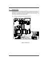
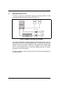
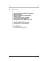
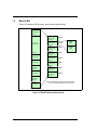
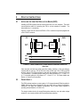
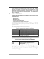
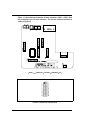
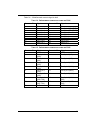
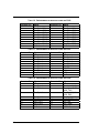
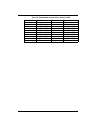
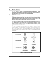
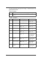
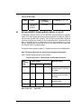
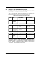
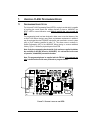
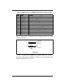
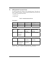
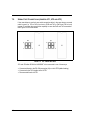
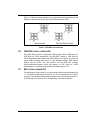
EVB2633F
USER MANUAL
FOR H8S/2633F
ON-CHIP FLASH MICROCONTROLLER
PREFACE
Product Warranty
The warranty periods against defects in materials and workmanship are as set out in the
accompanying Customer Information sheet.
Limitation of Warranty
The foregoing warranty does not cover damage caused by fair wear and tear, abnormal storage
conditions, incorrect use, accidental misuse, abuse, neglect, corruption, misapplication, addition
or modification or by the use with other hardware or software, as the case may be, with which the
product is incompatible. No warranty of fitness for a particular purpose is offered. The user
assumes the entire risk of using the product. Any liability of Hitachi Micro Systems Europe Limited
is limited exclusively to the replacement of defective materials or workmanship.
Restrictions
Hitachi Micro Systems Europe Limited's products are not authorised for use in medical
applications without prior written consent. Such use includes, but is not limited to, life support
systems.
Hardware Considerations
Appropriate care should be taken not to expose the EVB to moisture, extremes of temperature or
electrostatic discharge. Before opening the case, ensure that the unit is disconnected from
the power supply to prevent accidental damage.
1.
2.
3.
Earthing
This hardware is designed for use with equipment that is fully earthed. Ensure that all
equipment used is appropriately earthed. Failure to do so could lead to danger for the
operator or damage to equipment.
Electrostatic Discharge Precautions
This hardware contains devices that are sensitive to electrostatic discharge. Ensure
appropriate precautions are observed during handling and accessing connections. Failure to
do so could result in damage to the equipment.
Electromagnetic Compatibility
Operation of this hardware with any casing removed invalidates the conformity of the
equipment to the Electromagnetic Compatibility Directive 89/336/EEC.
It is advised that in this mode of operation suitable EMC precautions be observed.
Cautions
1. This document may be, wholly or partially, subject to change without notice.
2. All rights reserved. No one is permitted to reproduce or duplicate, in any form, a part or this
entire document without Hitachi Micro Systems Europe Limited's written permission.
2
Trademarks
1. General
All brand or product names used in this manual are trademarks or registered trademarks of
their respective companies or organisations.
2. Specific
Microsoft, MS and MS-DOS are registered trademarks and Windows and Windows NT are
trademarks of Microsoft Corporation.
IBM is a registered trademark of International Business Machines Corporation.
ProComm® is a registered trademark of Datastorm Technologies.
Lid and Chassis Removal
The metal chassis lid can be removed by extracting the four-crosshead screws around the sides two on each side of the lid. This gives access to all the jumpers on the EVB.
The PCB itself is held in the chassis by three crosshead screws that attach the PCB to the steel
pillars. The Serial Port is held in place by two hexagonal nuts attaching it to the front of the
chassis. The power supply wires from the 4mm sockets at the rear of the chassis are attached to
the PCB via a connector block.
To remove the PCB completely from the chassis:
1.
2.
3.
4.
5.
Remove the three screws from the PCB holding pillars.
Undo the connector block screws and retract the two wires BE SURE TO MAKE A NOTE
OF THE POLARITY, IT MAY NOT BE MARKED CLEARLY ON THE PCB.
Extract the two hexagonal nuts from the front of the chassis either side of the connector.
Retract the PCB from the front of the chassis towards the back until the connector, LEDs
and switches are clear.
The PCB can now be removed from the chassis.
Removing the FLASH Programming board
The FLASH Programming board is connected by a 14-way connector to the main PCB. To
remove it, first remove the metal chassis (see above), and then pull the two PCBs gently apart.
Document Information
Product Code:
D001228_11
Version:
1.0
Date:
January 2000
Copyright © Hitachi Micro Systems Incorporated. 1994-1999. All rights reserved.
Copyright © Hitachi Micro Systems Europe Ltd. 1995-1999. All rights reserved.
Copyright © Hitachi Europe Ltd. 1995-1999. All rights reserved.
3
TABLE OF CONTENTS
GETTING STARTED ............................................................................................................................. 7
1.
INTRODUCTION .................................................................................................................... 11
1.1 EVB FUNCTIONAL BLOCKS .................................................................................................. 12
1.2 SPECIFICATIONS.................................................................................................................. 13
1.2.1
GENERAL .......................................................................................................... 13
1.2.2
RS232 COMMUNICATIONS ................................................................................. 13
1.2.3
POWER ............................................................................................................. 13
1.3 MEMORY MAP ..................................................................................................................... 14
2.
START-UP INSTRUCTIONS .................................................................................................... 15
2.1 INSTALLING THE LOW COST EVALUATION BOARD (EVB)....................................................... 15
2.2 POWER SUPPLY .................................................................................................................. 15
2.3 SOFTWARE INSTALLATION ................................................................................................... 16
2.4 INSTALLATION OF CD-ROM SOFTWARE ............................................................................... 16
3.
PRINCIPLES OF OPERATION ................................................................................................. 17
3.1 H8S/2633F MICROCONTROLLER......................................................................................... 17
3.2 CLOCK CIRCUITRY............................................................................................................... 17
3.3 COLD RESET CIRCUITRY ..................................................................................................... 18
3.4 NMI CIRCUITRY .................................................................................................................. 18
3.5 INTERRUPT REQUEST CIRCUITRY......................................................................................... 19
3.6 RAM .................................................................................................................................. 19
3.7 SERIAL INTERFACE .............................................................................................................. 20
3.8 LEDS.................................................................................................................................. 20
3.9 EXTERNAL USER INTERFACE ............................................................................................... 21
4.
BOARD OPTIONS ................................................................................................................. 27
4.1 EVB2633F JUMPERS.......................................................................................................... 27
4.2 SETTING H8S/2633F OPERATING MODE (JUMPERS, J1 AND J2) ......................................... 29
4.3 ANALOGUE REFERENCE AND SUPPLY (JUMPERS, J3 – J5)................................................... 30
4.4 AVCC, ANALOGUE SUPPLY JUMPER, J3 .............................................................................. 30
4.5 AVSS, ANALOGUE GROUND JUMPER, J4 ............................................................................. 30
4.6 VREF, ANALOGUE REFERENCE JUMPER, J5......................................................................... 30
4.7 LED CONTROL JUMPERS (J6 AND J11) ............................................................................... 30
4
4.7.1
RED LED CONTROL JUMPER, J6 .......................................................................30
4.7.2
GREEN LED CONNECTION JUMPER, J11 ............................................................31
4.7.3
TXD AND RXD CONNECTION ORIENTATION JUMPER, J7....................................31
4.7.4
RESET INPUT CONTROL JUMPER, J8................................................................31
4.7.5
NMI INPUT CONTROL JUMPER, J9 .....................................................................31
4.7.6
IRQ0 INPUT CONTROL JUMPER, J10 .................................................................31
4.8 UNIVERSAL FLASH PROGRAMMING BOARD JUMPERS .........................................................32
5.
CODE DEVELOPMENT ..........................................................................................................35
5.1 HOST COMPUTER SPECIFICATIONS ....................................................................................35
5.2 TUTORIALS ..........................................................................................................................35
5.3 ADDITIONAL INFORMATION ...................................................................................................36
6.
HDI MONITOR .....................................................................................................................37
6.1 INTRODUCTION TO HDI-M....................................................................................................37
6.2 PROGRAM DEVELOPMENT ...................................................................................................37
6.3 USING HDI-M......................................................................................................................37
7.
UNIVERSAL FLASH PROGRAMMING BOARD .........................................................................39
7.1 PROGRAMMING BOARD OPTION ...........................................................................................39
7.2 UFPB INTERFACE ...............................................................................................................40
7.3 UFPB OPERATION ..............................................................................................................42
7.4 TRANSPARENT MODE AND THE PMODE PIN ........................................................................42
7.5 OPERATION DURING H8S/2633F INITIALISATION TO BOOT, USER & NORMAL MODES ........43
7.6 OPERATION DURING PROGRAMMING KERNEL EXECUTION .....................................................44
7.7 PROGRAMMING SOFTWARE OPERATION...............................................................................44
7.8 UFPB JUMPER SETTINGS AND OPTIONS ..............................................................................45
7.9 SERIAL PORT CONNECTIONS (JUMPERS JP1, JP2 AND JP3)................................................46
7.10 FWE/FWP CONTROL (JUMPER JP4)...................................................................................47
7.11 MDX CONTROL (JUMPER JP5).............................................................................................47
5
GETTING STARTED SECTION
INTRODUCTION
This section is intended to help the user to get started quickly when using the H8S/2633F EVB. It
will cover how to:
•
•
•
Build an executable file.
How to download an executable file to the board.
How to FLASH the EVB using the Universal FLASH Programming Board (UFPB).
There are five major parts to the H8S/2633F EVB CD:
1.
2.
3.
4.
5.
Hitachi Embedded Workshop (HEW) build environment.
Hitachi C Compiler (evaluation copy) and IAR Compiler (demo version).
Hitachi Debugging Interface (HDI-M).
FLASH Development Toolkit (FDT).
Tutorials and User Manuals.
The HEW Installation on the CD contains two compilers: Hitachi C Compiler and IAR Compiler,
both of which are supported by the HEW build environment. The European market supports use
of the IAR compiler, whilst the US market supports use of Hitachi C Compiler (evaluation copy).
In order to use the Hitachi C Compiler, an initiating file must be obtained from Hitachi
Semiconductor (America) Inc. Technical Support Center.
BUILDING AN EXECUTABLE FILE
The following instructions show you how to build an example executable file using HEW with
either the IAR Compiler or the Hitachi C Compiler. You will need to have installed the Hitachi
Embedded Workshop, from the CD Menu Program (Menu.exe), “Install Software\Hitachi
Embedded Workshop”.
•
•
•
•
•
•
•
Start HEW by clicking on the Start Menu, navigate to and select “Hitachi Embedded
Workshop”.
At the “Welcome” dialog select “Create a new project workspace”
Enter a project name, e.g. FLASHER
The default directory, therefore, will be “C:\FLASHER\”.
It is suggested that the user creates a project directory structure such as
c:\hewdemo\evb2633f\tutorials\. The FLASHER directory then becomes a sub-directory of
Tutorials.
Select CPU Family : “H8S,H8/300”
Select preferred Toolchain :
- US Customers select : “Hitachi H8S, H8/300 Standard”
- European Customers select : “IAR ICCH8 (H8S, H8/300H)”
6
•
•
Select Project Type : “EVB2633”
Select OK.
The EVB2633F Project Generator will set up the correct environment for EVB2633F project.
•
•
•
•
Select type of project you prefer : “Complete Projects”
Select tutorial for project generation : “FLASHER”
Select “Finish”
Select “OK”
The Workspace window shows the files associated with the Flasher Tutorial Program, i.e. source
files, header files etc. To view the source file in the editor window: select “b_flasher.c”.
To build an executable file:
•
Select “Build…Build All” from the menubar.
The output window will indicate when the build is complete and successful.
An executable file flasher.abs (from Hitachi C Compiler) or Flasher.d37 (from IAR Compiler) file
will be created that will FLASH the green LED when downloaded to the H8S/2633F device.
Note - If you encounter the following message: “Cannot open Time Key File; Please reinstall or specify “HITACHI=directory” as an environment value”:
Please ensure you have the Time Key File that can be obtained from Hitachi
Semiconductor (America) Inc. Technical Support Centre.
DOWNLOADING AN EXECUTABLE FILE
The following procedure explains how to download the executable file you have just built to the
H8S/2633F device.
To set up a link between the HDI-Debugger and the EVB you first need to:
•
•
•
•
•
Ensure mode jumpers are set for mode 6 (jumper settings for J4-J6 are found at the end of
this section)
Connect the host PC to the SCI0 port on the EVB and power up the EVB.
Run HDI-M by clicking on the Launch Debugger icon on the HEW toolbar
A new session is created and the built file is loaded automatically on “H8S/2600 Monitor”
A successful link between the HDI-M debugger and the EVB will be indicated with a “Link
Up” message in the Status Bar (found in the bottom left hand corner of the HDI-M window).
Note - If the EVB cannot link up by itself a “Monitor Setup:” dialog box will appear,
insert the COM port information and the baud rate – 38400 and select OK.
7
•
If, after continued attempts the debugger fails to connect, it is probable that HDI-M monitor is
not loaded into the EVB. To load the HDI-M monitor into the H8S/2633F device please run
through the section: “FLASH Programming the Device”. This will reprogram the FLASH
device on the EVB2633F with the HDI Monitor embedded kernel.
TO DOWNLOAD YOUR EXECUTABLE FILE TO THE H8S/2633F DEVICE
Select from the HDI menu: “File…Load Program…” your preferred file from directory:
“C:\hewdemo\evb2633f\tutorials\flasher\flasher\Debug”
•
•
•
US Customers select “flasher.abs”
European Customers select “flasher.d37”
A box will appear providing details of memory “Areas Loaded”. Select OK.
To run the program the following steps must be taken:
•
•
•
•
Select “View…Source” from the menubar and select the source file “b_ flasher.c” from
C:\hewdemo\evb2633f\tutorials\flasher\flasher.
Click on the “main” label of the source file and select “Run…Set PC to Cursor”. A yellow
highlight will appear over the line of code.
Select “Run…Go” from the HDI menubar.
The green LED on the EVB will start flashing.
FLASH PROGRAMMING THE DEVICE
This process will be necessary if the user wishes to connect to the EVB with HDI monitor. Please
connect the EVB device in the BOOT mode ready to reprogram the FLASH, and download the
correct program as follows:
•
•
•
•
•
•
8
Install the FLASH Development Software Tool (FDT) from “Install Software\Flash
Development Toolkit”.
Apply power to the EVB, this is done via the red and black socket located at the rear of the
unit, (+5V only).
Connect the serial cable to a COM port on the PC and to the SCI2 (different than the normal
downloading port) connector on the EVB. The jumpers on the EVB must be in the default
position (factory settings).
Run the FDT software from the Start menu.
Select “Open an existing image file” in order to download a single file.
The lower box in the window will allow you to select “More files…”. Use this to open the Srecord HDI-Monitor file “2633m6.mot”. This can be found by exploring the CD-ROM drive,
HDI-M directory.
•
To download the image select “IMAGE…Download Image…” and configure the device :
-
•
Target Device: H8S/2633F
User Settings: COM port connected to the PC
Use Default Settings: UNCHECKED
Baud Rate: 38400 BAUD
Connection: BOOT
Select Interface: HMSE UFPB
Kernel already resident: UNCHECKED
Click the “CONNECT” button. The FLASH device is now in BOOT mode and ready to be
programmed.
Select “Download file 2633m6.mot to device”.
You are asked if you wish to perform a readback : select “Y”
The HDI_H8S2600 monitor kernel for the CPU is now programmed into the FLASH memory
of the H8S/2633F device. You are now able to link to HDI and download files as described
above.
Select “Disconnect” for ending the programming procedure.
Close the FDT programming software and reset the EVB by pressing the CRES switch on
the EVB.
Now switch off the EVB power supply.
•
•
•
•
•
•
Please note it is important to disconnect the FDT software from the EVB before pressing
the CRES switch. Not doing so may corrupt the program and necessitate repeating the
process.
The above is just a brief getting started note, please read the EVB2633F User Manual for more
information.
DEFAULT JUMPER SETTINGS
Two-pin in-line jumpers
Jumper
J11
Use
J6
Pins
1-2
Fitted
Three-pin in-line jumpers
Jumper
J1
Use
MD1 tied to Vcc
J2
MD0 tied to ground
J3
Avcc tied to Vcc
J4
Avss tied to ground
J5
Vref tied to Vcc
Pins
1-2
Fitted
2-3
Fitted
1-2
Fitted
1-2
Fitted
1-2
Fitted
J8
J9
J10
LED connected to
ground
Reset activated by
SW1
NMI activated by
SW2
IRQ0 activated by
SW3
1-2
Fitted
1-2
Fitted
1-2
Fitted
1-2
Fitted
Four-pin jumpers
Jumper
J7
Use
1:1 TXD and RXD
connection
Pins
1-2, 3-4
Fitted
9
1.
INTRODUCTION
The H8S/2633F low-cost evaluation board (EVB) is an inexpensive demonstration and
evaluation tool for the Hitachi H8S/2000 family of high performance microcontrollers. It
incorporates a programming system for the H8S/2633F on-chip FLASH device. The
EVB contains a H8S/2633F device (HD64F2633F).
Fig. 1.1 EVB Layout illustrates the physical layout of the EVB.
FIGURE 1.1 EVB LAYOUT
11
1.1
EVB FUNCTIONAL BLOCKS
The EVB is composed of an H8S/2633F single-chip microcontroller, RAM, a FLASH
programming interface board and two serial ports (Figure 1.2).
FIGURE 1.2 EVB2633F FUNCTIONAL BLOCK DIAGRAM
The on-chip FLASH memory contains the firmware monitor program, HDI-M. Two bytewide RAM devices provide word-wide read and writes. Two three-wire serial ports are
supported using two of the on-board H8S/2633F serial communications interface (SCI)
devices. One serial port (SCI0 – Host Port) is dedicated to the on-board HDI-M
monitor, the second serial port (SCI2 – User Port) is available to the user, or is used to
program the on-chip FLASH memory.
The Windows debugger, HDI, will connect to HDI-M to provide high-level debugging via
the Host port (SCI0).
12
1.2
SPECIFICATIONS
1.2.1
•
•
•
•
•
•
•
25MHz (max) H8S/2633F processor (using HD64F2633F device)
256Kbytes external RAM
256Kbytes FLASH ROM with the HDI-M firmware monitor
16Kbytes on-chip RAM
Two LED indicators and three push button switches
Detachable FLASH programming interface board
All practical H8S/2633F signals available for user connection
1.2.2
•
•
RS232 COMMUNICATIONS
Host (SCI0) interface via RS-232 DB-9S connector
User (SCI2) interface via RS-232 DB-9S connector
1.2.3
•
•
GENERAL
POWER
5V DC-only power supply
Power connection via 4mm standard plugs
13
1.3
MEMORY MAP
Figure 1.3 illustrates the EVB memory map for mode 6 (default mode).
H’000000
On-Chip ROM
H’03FFFF
H’040000
External
Address Space
H’000000
Area 0 (CS0)
H’1FFFFF
H’200000
Area 1 (CS1)
H’3FFFFF
H’400000
Area 2 (CS2)
H’5FFFFF
H’FFAFFF
H’FFB000
On-Chip RAM*
H’FFEFC0
External Area
H’FFF800
Internal I/O
Registers
H’FFFF40
External Area
H’FFFF60
H’600000
Area 3 (CS3)
H’7FFFFF
H’800000
Area 4 (CS4)
H’9FFFFF
H’A00000
Area 5 (CS5)
H’BFFFFF
H’C00000
Area 6 (CS6)
H’DFFFFF
H’E00000
Area 7 (CS7)
H’FFFFFF
2MBytes
2MBytes
SRAM 1
1Mbit
2MBytes
SRAM 2
1Mbit
2MBytes
2MBytes
2MBytes
2MBytes
2MBytes
Internal I/O
Registers
H’FFFFC0
On-Chip RAM*
NOTE: *On-Chip RAM can be used as external address
space by clearing the RAME bit in the SYSCR to 0.
Figure 1.3 EVB2633F Memory Map (mode 6)
14
2.
START-UP INSTRUCTIONS
2.1
INSTALLING THE LOW COST EVALUATION BOARD (EVB)
Installing the EVB requires power and serial connection to a host computer. The serial
communications cable for connecting the EVB to a host computer is supplied. The
serial cable has 1:1 connectivity.
Figure 2.1 shows how to connect the EVB to a PC or notebook computer equipped with
a ‘mini’ DB-9P connector.
EVB
PC
9-pin
DB-P
DB9S
9-pin
DB-9S
DB9P
3
3
RXD
2
2
RXD
GND
5
5
GND
TXD
TXD
FIGURE 2.1 : SERIAL CONNECTION TO PC/NOTEBOOK WITH MINI DB-9 CONNECTOR
(SUPPLIED)
Users may also use their own serial connection cables, if desired. In the case where a
crossed cable is used (i.e. TXD to RXD from Host to EVB, and TXD to RXD from EVB
to Host), jumper J7 for SCI0 provides the user with the capability to cross the RXD and
TXD connections. The default jumper setting is for direct connection (J7: 1-3 and J7: 24). For crossed cable use, set jumper to J7: 1-2 and J7: 3-4. For further details see
Section 4.1 Serial Port Connections.
2.2
POWER SUPPLY
The EVB hardware requires a power supply of +5V at approximately 250mA supplied to
CON2. Since total power consumption can vary widely due to external connections,
H8S/2633F port state, and memory configuration, use a power supply capable of
providing at least 600mA at +5V DC ± 5%.
The design includes circuitry for supply filtering/noise reduction, over and under voltage
protection, over current protection and reversed polarity protection.
15
A 3.3V voltage regulator is also incorporated into the power supply circuitry, to generate
the 3.3V required to operate the H8S/2633F microcontroller.
Caution: A power supply with current limiting and an active current display is
recommended when the EVB is used for hardware experimentation. The EVB is
provided with polarity reversal protection. If the EVB does not consume any
current, check the power connection for polarity reversal.
The power connector on the EVB is connected to 4mm sockets mounted in the casing.
Standard 4mm plugs may be used to connect to a bench power supply.
2.3
SOFTWARE INSTALLATION
Please review the following procedures thoroughly before installing. Software is
supplied with the EVB on a CD-ROM. Users should make sure their system has a CDROM drive correctly installed before continuing.
The CD-ROM includes the following software:
1.
2.
3.
4.
2.4
HDI-M Windows Debugger
Hitachi Embedded Workshop including Hitachi/MCS and IAR Series C compiler
FLASH Development Toolkit (FDT)
EVB Tutorials
INSTALLATION OF CD-ROM SOFTWARE
An installation utility is supplied with the CD-ROM, enabling the user to easily install all
components of the EVB2633F. For using this installation utility, please refer to the CDROM insert.
To manually install the components listed above, please note the locations of the setup
utilities:
•
•
•
•
HDI-M Windows Debugger
HEW
FDT
Tutorials
D:\HDIM\SETUP.EXE
D:\HEWDEMO\SETUP.EXE
D:\FDT\SETUP.EXE
D:\Tutorials\Install.exe
Note: The default installation directory for
C:\HWBDEMO\TUTORIALS\… as used in the tutorial.
16
the
tutorial
file
is
3.
PRINCIPLES OF OPERATION
The EVB is composed of the following components:
•
•
•
•
•
•
•
•
•
•
H8S/2633F Microcontroller
Clock Circuitry
Cold Reset (CRES) circuitry
Non Maskable Interrupt (NMI) Circuitry
Interrupt Request (IRQ0) Circuitry
On-board RAM
Detachable Programming Interface Board
Serial Interfaces
LED Driver
External User Interface
The complete EVB schematics are provided as part of the kit and are referenced
throughout this chapter.
3.1
H8S/2633F MICROCONTROLLER
The H8S/2633F series of high-performance single-chip microcontrollers have a wide
variety of on-chip peripheral functions. The on-chip supporting functions include
FLASH ROM, RAM, 16-bit timer pulse unit (TPU), programmable pulse generator
(PPG), an 8-bit timer, a 14 bit PWM timer (PWM), a watchdog timer (WDT), five serial
communications interfaces (SCI’s, IrDA), an A/D converter, a D/A converter, I/O ports, a
DMA controller (DMAC) and other facilities.
Users reconfiguring processor I/O ports are cautioned that pull-up resistors may be
required for correct operation in some configurations.
On the EVB2633F, the H8S/2633F internal FLASH memory is pre-programmed with the
HDI-M debugging monitor. HDI-M may be used to download, run and debug programs
developed on a host computer.
3.2
CLOCK CIRCUITRY
The EVB uses a quartz crystal (18.432MHz) in conjunction with capacitors C7 and C8
to provide the clock signal for the H8S/2633F. The PLL multiplier is set for a
multiplication factor of x1 fixed. The system clock (CLK, pin 90) output frequency is the
same as that of the internal operating frequency (18.432MHz).
The CLK clock is also available for external use via connector CON8, pin 18.
A 32.768KHz quartz oscillator is connected, in conjunction with capacitors C5 and C6,
to the H8S/2633F to provide a clock to the subclock divider.
17
3.3
COLD RESET CIRCUITRY
The reset generator for the EVB is based on the 7705A Supply Voltage Supervisor from
Texas Instruments. This chip is specifically designed for use as a reset controller in
microcomputer and microprocessor systems.
During power-up the device monitors the supply voltage and keeps the RESET and
RESETn outputs active (high and low respectively) as long as the supply voltage has
not reached its nominal value. After the voltage has reached the tolerance, the RESET
and RESETn signals are kept active for an additional 60ms to allow for final supply
stabilisation and microcontroller reset. Typically the H8S/2633F RESn signal requires
at least 1.30µs to reset and the clock oscillator requires at least 10ms to stabilise.
The threshold voltage is 4.5V +_ 50mV with a hysteresis of 15mV. If there is a voltage
drop on the supply the RESETn will be activated. When the supply recovers and
passes the threshold the RESETn will remain active for another 60ms period.
There is also a push-button switch, SW1, to generate a cold reset (CRESn). The switch
is debounced in two cross-coupled NAND gates (U8, pins 1,2,4 & 5) and fed to the
RST_IN input of the 7705A. When the push-button is released the 7705A will provide a
60ms reset signal.
The 7705A output is NANDed with the FLASH_RESET signal from the universal
FLASH programming board to generate the final RESETn signal to the microcontroller.
This RESETn signal is also fed back to the universal FLASH programming board. If
the universal programming board is not present a pull-up resistor deactivates the
FLASH-RESET signal.
Quickly switching power to the board off and then on again quickly may not allow VCC
to fall low enough to generate a reset pulse. In practice, the H8S/2633F usually
continues to operate normally. Rapid on/off switching of the power supply stresses
the integrated circuit components and is not recommended.
Alternatively, driving the Cold Reset signal from an external source is possible via
jumper 8 and connector CON8, pin 12.
3.4
NMI CIRCUITRY
The NMI input of the H8S/2633F is an independent edge-triggered input. NMI may be
generated on the positive or negative going transition, dependent upon the setting of
the System Control Register (SYSCR) NMIEG bit. Default after reset is interrupt
request generation on the negative going edge of the NMI input.
The EVB uses two cross-coupled NAND gates (U9, pins 1, 2,4 & 5) to debounce the
output of momentary push- button switch SW2. In the quiescent state, the output of U9,
pin 3 (and thus the H8S/2633F NMI input) is high. Closing SW2 causes the NMI signal
to go low until SW2 is released.
18
Alternatively, Jumper J9 can be used to enable driving of the NMI signal from an
external source via connector CON8, pin 14. Refer to Section 4 for details.
3.5
INTERRUPT REQUEST CIRCUITRY
The IRQ0 signal (Interrupt Request 0) of the H8S/2633F is multiplexed with Port 1, pin
4. Setting IRQ Enable Register (IER) bit 0 to 1 will enable IRQ0 interrupt requests and
ensure that an interrupt will be generated when IRQ0 is activated.
IRQ0 can be set to generate an interrupt request on an input low level, on a rising edge
input, on a falling edge input, or on both rising and falling edges of an input. Specific
selection occurs by setting the appropriate IRQ Sense Control Register (ISCRL), IRQ0
bits (0 and 1). The default value is to generate an interrupt request on an input low
level.
The EVB uses two cross-coupled NAND gates (U9, pins 9, 10, 12 & 13) to debounce
the output of momentary push- button switch SW3. In the quiescent state, the output of
U9, pin 8 (and thus the H8S/2633F IRQ0 input) is high. Closing SW3 causes the IRQ0
signal to go low until SW3 is released.
Alternatively, Jumper J10 can be used to enable driving of the IRQ0 signal from an
external source via connector CON8, pin 16. Refer to Section 4 for details.
3.6
RAM
The RAM devices U4 and U5, which are, by default, a pair of 128k x 8 static CMOS
RAM organised for word-wide access. (Figure 1.3 illustrates the memory map)
The external RAM is located at H’0020 0000 – H’0023 FFFF in CS1 space. When RAM
is referenced at this address, the memory area chip select signal CS1n, and RDn or
LWRn or HWRn signals are generated by the H8S/2633F. CS1n and RDn signals are
connected to both U4 and U5. The LWRn (write low byte) signal is connected to SRAM
device U4 which is connected to databus D0-D7, whilst the HWRn (write high byte)
signal is connected to SRAM device U5 which is connected to databus D8-D15.
The CS1 space size must be specified to allow 16-bit access. Bus Width Control
Register (ABWCR), bit 1 must be set to 0 to specify the 16-bit access. The default
setting after power-on reset is for 8-bit access only.
The default RAM capacity of 2 x (128k x 8) may be increased to 2 x (512k x 8) by
substituting larger static CMOS RAM devices for U4 and U5. If the larger devices are
fitted R8 should be removed from the board and resistors R6 and R7 fitted. R6 and R7
are both 0805 size surface mount zero ohm resistors.
Note: The value of Wait Control Register 1 (WCRL) bits W11 and W10 specify the
number of wait-states (0-3 cycles) for the CS1 space. The default value is B’11. It
should be set to B’00 to specify no wait. This is due to the selected access speed
of the RAM memory of 55ns and this makes it possible to access the RAM
memory without any wait-states.
19
3.7
SERIAL INTERFACE
The EVB supports two three-wire serial channels using two of the five identical SCI
modules, SCI0 and SCI2, in the H8S/2633F microcomputer. SCI0 is normally
dedicated for use by HDI-M for communication with a host PC.
SCI2 is required for BOOT mode operation of the H8S/2633F, and otherwise is
available to the user.
SCI0 signals are connected to U6 (MAX232) which is a serial transceiver device that
translates logic levels to RS-232 levels and vice-versa. The RS-232 signal for the
HOST port is connected to a DB-9S type connector (CON3).
SCI2 signals are routed via the Universal FLASH Programming Board. Normally the
host terminal communication is carried out via the H8/3217 device on the FLASH
Universal Programming Board. On this board a transceiver (MAX232) circuit translates
to RS-232 levels. The RS-232 signals for the USER port are connected to a DB-9S
type connector, J4. (See Figure 7.1)
SCI2 can alternatively be used as a USER port. Jumpers JP2 and JP3 on the
Universal FLASH Programming Board can be reconfigured to bypass the H8S/3217
device. Consequently the H8S/2633F microcontroller can directly access the RS-232
port on the UFPB and the FLASH memory on the H8S/2633F will not be programmed.
Jumper JP4 must also be reconfigured with the socket connecting pin 2-3.
See Section 7 for further details on Universal FLASH Programming Board operation.
Table 3.1 defines EVB2633F RS-232 Interface Signals.
TABLE 3.1 : RS-232 INTERFACE CONNECTORS
Connector
CON3
J4(UFPB)
3.8
Signals
SCI0
SCI2
LEDS
Two LEDs are incorporated on the EVB to display board status. A FCT244 buffer (U3)
is used to drive the LEDs as the H8S/2633F ports are unable to.
The green LED (LED1) can be activated from Port 1, 5 via the buffer and a current
limiting resistor. LED1 will be turned ON when P1, 5 is driven low. Jumper, J11 is
inserted by default. Removal of J11 frees Port 1, 5 for alternative use.
20
The red LED (LED2) can be activated as either a Power or a User LED. The default
option (pins 1-2) of jumper, J6 will connect LED2 across the power supply and will
indicate power is supplied to the EVB2633F. The alternative option (pin 2-3) connects
LED2 to Port 3, 2 via the buffer and a current limiting resistor. LED2 will be turned ON
when P3, 2 is driven low.
3.9
EXTERNAL USER INTERFACE
The external user interface makes most of the H8S/2633F signals available to the user
consistent with keeping:
•
•
•
•
Signal lines short
Board design simple
Functional signals grouped together
Lines potentially used for analogue signals isolated
The external user interface consists of six two-row connectors of 20 pins each.
Commonly available 2.54mm (0.100 inch) male headers with 0.635mm (0.25 inch)
square posts are used.
Table 3.2 defines address and data connectors and signals.
TABLE 3.2: ADDRESS AND DATA CONNECTORS AND SIGNALS
CONNECTOR
CON4
CON5
CON6
CON7
CON8
CON9
SIGNALS
Port 1 (7:0) / Port 3 (7:0)
Port 4 (7:0) / Port 9 (7:0) / AVCC / AVSS / VREF
Port D (7:0) / Port E (7:0)
Port F (7:0) / Port G (4:0) / RESETn / NMI / STBYn
Port 7 (7:0) / Port A (3:0) / EXT_RESETn / EXT_NMI /
EXT_IRQ0n / CLK / WDTOVFn
Port B (7:0) / Port C (7:0)
Table 3.3 defines interface connectors for Serial and Power Signals
TABLE 3.3: INTERFACE CONNECTORS: SERIAL AND POWER SIGNALS
CONNECTOR
CON1
CON2
CON3
SIGNALS
Universal Programming Board Connector [SCI2]
Power Connector
9-way D-type (RS232) [SCI0]
Note: Each of these external interface connectors also includes VCC, normally at
+5V and GND. Trivial external circuits may use power from the EVB. However, if
more that 50mA is needed the external circuits should be powered by an
independent power supply.
21
Figure 3.1 shows the board locations of these connectors CON1 – CON9. Note
the positioning of pin 1 on each connector. The pins are numbered odd-even as
shown in Figure 3.2.
FIGURE 3.1 CONNECTOR LOCATIONS (COMPONENT SIDE)
FIGURE 3.2 CONNECTOR CONFIGURATION
22
Tables 3.4 – 3.9 defines each connector signal in detail
TABLE 3.4: PIN ASSIGNMENT FOR INTERFACE CONNECTOR CON4
Connector Pin
Signal
Connector Pin
Signal
1
3
5
7
9
11
13
15
17
19
5V
Port 1, pin 0
Port 1, pin 1
Port 1, pin 2
Port 1, pin 3
Port 1, pin 4
Port 1, pin 5
Port 1, pin 6
Port 1, pin 7
GND
2
4
6
8
10
12
14
16
18
20
5V
Port 3, pin 0 (SCI0_TXD)
Port 3, pin 1 (SCI0_RXD)
Port 3, pin 2
Port 3, pin 3
Port 3, pin 4
Port 3, pin 5
Port 3, pin 6
Port 3, pin 7
GND
TABLE 3.5: PIN ASSIGNMENT FOR INTERFACE CONNECTOR CON5
Connector Pin
Signal
Connector Pin
Signal
1
3
AVCC
Port 4, pin 0
(AN0)
Port 4, pin 1
(AN1)
Port 4, pin 2
(AN2)
Port 4, pin 3
(AN3)
Port 4, pin 4
(AN4)
Port 4, pin 5
(AN5)
Port 4, pin 6
(AN6 / DA0)
Port 4, pin 7
(AN7 / DA1)
GND
2
4
VREF
Port 9, pin 0 (AN8)
6
Port 9, pin 1 (AN9)
8
Port 9, pin 2 (AN10)
10
Port 9, pin 3 (AN11)
12
Port 9, pin 4 (AN12)
14
Port 9, pin 5 (AN13)
16
Port 9, pin 6 (AN14 /
DA2)
Port 9, pin 7 (AN15 /
DA3)
AVSS
5
7
9
11
13
15
17
19
18
20
23
TABLE 3.6: PIN ASSIGNMENT FOR INTERFACE CONNECTOR CON6
Connector Pin
1
3
5
7
9
11
13
15
17
19
Signal
5V
Port D, pin 0 (D8)
Port D, pin 1 (D9)
Port D, pin 2 (D10)
Port D, pin 3 (D11)
Port D, pin 4 (D12)
Port D, pin 5 (D13)
Port D, pin 6 (D14)
Port D, pin 7 (D15)
GND
Connector Pin
2
4
6
8
10
12
14
16
18
20
Signal
5V
Port E, pin 0 (D0)
Port E, pin 1 (D1)
Port E, pin 2 (D2)
Port E, pin 3 (D3)
Port E, pin 4 (D4)
Port E, pin 5 (D5)
Port E, pin 6 (D6)
Port E, pin 7 (D7)
GND
TABLE 3.7: PIN ASSIGNMENT FOR INTERFACE CONNECTOR CON7
Connector Pin
1
3
5
7
9
11
13
15
17
19
Signal
5V
Port F, pin 0
Port F, pin 1
Port F, pin 2
Port F, pin 3
Port F, pin 4
Port F, pin 5
Port F, pin 6
Port F, pin 7
GND
Connector Pin
2
4
6
8
10
12
14
16
18
20
Signal
5V
Port G, pin 0
Port G, pin 1
Port G, pin 2
Port G, pin 3
Port G, pin 4
RESETn
NMI
STBYn
GND
TABLE 3.8: PIN ASSIGNMENT FOR INTERFACE CONNECTOR CON8
24
Connector Pin
1
3
5
Signal
5V
Port 7, pin 0
Port 7, pin 1
Connector Pin
2
4
6
7
Port 7, pin 2
8
9
11
13
15
17
19
Port 7, pin 3
Port 7, pin 4
Port 7, pin 5
Port 7, pin 6
Port 7, pin 7
GND
10
12
14
16
18
20
Signal
5V
Port A, pin 0 (A16)
Port A, pin 1 (A17 /
SCI2_TXD)
Port A, pin 2 (A18 /
SCI2_RXD)
Port A, pin 3 (A19)
EXT_RESETn
EXT_NMI
EXT_IRQ0n
CLK
WDTOVFn
TABLE 3.9: PIN ASSIGNMENT FOR INTERFACE CONNECTOR CON9
Connector Pin
1
3
5
7
9
11
13
15
17
19
Signal
5V
Port B, pin 0 (A8)
Port B, pin 1 (A9)
Port B, pin 2 (A10)
Port B, pin 3 (A11)
Port B, pin 4 (A12)
Port B, pin 5 (A13)
Port B, pin 6 (A14)
Port B, pin 7 (A15)
GND
Connector Pin
2
4
6
8
10
12
14
16
18
20
Signal
5V
Port C, pin 0 (A0)
Port C, pin 1 (A1)
Port C, pin 2 (A2)
Port C, pin 3 (A3)
Port C, pin 4 (A4)
Port C, pin 5 (A5)
Port C, pin 6 (A6)
Port C, pin 7 (A7)
GND
25
26
4.
BOARD OPTIONS
The EVB provides a number of user-definable optional configurations. These
configurations are selectable by jumper settings and zero ohm resistors on EVB2633F
and jumper settings on the Universal FLASH Programming Board.
4.1
EVB2633F JUMPERS
EVB jumpers allow users to configure the board as required for testing or evaluation.
Three types of jumper are used: 2-pin, 3-pin in-line and 4-pin blocks. The default setting
for the 2-pin jumpers is when the jumper socket is connected across pins 1 and 2. The
alternative setting is when the jumper socket is removed from the board.
The 3-pin in-line jumpers are used to connect one of two possible signals to a third line.
The default setting for these jumpers (with the exception of J2) is when the jumper
socket is connected across pins 1 and 2. The alternative setting is when the jumper
socket is connected across pins 2 and 3.
The 4-pin blocks typically allow signal paths to be changed by rotating the jumper
sockets through 900. The default setting is for the jumper sockets to be connected from
pin 1 to pin 3 and pin 2 to pin 4. The alternative setting is for the jumper sockets to be
connected from pin 1 to pin 2 and pin 3 to pin 4. Figure 4.1 illustrates general jumper
configuration.
FIGURE 4.1: JUMPER CONFIGURATION
27
The following tables define each jumper and its settings. A detailed description of the
jumpers listed will then follow.
Two-pin in-line jumper
Jumper
Function
J11
Use of jumper connects Port1, pin 5 on H8S/2633F to user LED
(LED1).
Three-pin in-line jumpers
28
Jumper
Function
Default Setting
Alternative Setting
J1
H8S/2633F MD1
MD1 = 1 (Pins 1 – 2)
MD1 tied to ground
(Pins 2 – 3)
J2
H8S/2633F MD0
MD0 = 0 (Pins 2 – 3)
MD0 pulled to VCC
(Pins 1 – 2)
J3
AVCC Selection
AVCC tied to 5V
(Pins 1 – 2)
Connected to AVCC
(Pins 2 – 3)
J4
AVSS Selection
AVSS tied to GND
(Pins 1 – 2)
Connected to AVSS
(Pins 2 – 3)
J5
VREF Selection
VREF tied to 5V
(Pins 1 – 2)
Connected to VREF
(Pins 2 – 3)
J6
Red LED Control
Power Indicator
(Pins 1 – 2)
LED driven by
output of Port 3, pin
2 on H8S/2633F
(Pins 2 – 3)
J8
RESET Input
Control
Reset activated by SW1
(Pins 1 – 2)
Reset activated by
an external signal
(Pins 2 – 3)
J9
NMI Input Control
NMI activated by SW2
(Pins 1 – 2)
NMI activated by an
external signal
(Pins 2 – 3)
J10
IRQ0 Input
Control
IRQ0 activated by SW3
(Pins 1 – 2)
IRQ0 activated by
an external signal
(Pins 2 – 3)
Four-pin in-line jumper
4.2
Jumper
Function
Pin Setting (1 – 3,
2 - 4) (Default)
Pin Setting (1 – 2, 3 – 4)
J7
TXD and RXD
connection
orientation
1:1 connection
Crossed connection
SETTING H8S/2633F OPERATING MODE (JUMPERS, J1 AND J2)
As described in Sections 3 and 22 of the H8S/2633F Hardware Manual, the operating
modes of the microcontroller are set during device initialisation, by setting pin FWE and
the three mode pins MD0, MD1 and MD2. The FWE signal is pulled down to GND and
is normally sourced by the Universal FLASH Programming Board. Mode pins MD0 and
MD1 are jumpered (J2 and J1 respectively) to allow user modification of the mode
settings. Mode pin MD2 is pulled high but can be over-ridden by the MDy signal from
the Universal FLASH Programming Board.
The default mode of operation is Mode 6 – Expanded mode with on-chip ROM enabled.
Note: The inputs at the mode pins should not be changed during operation
Table 4.4 defines jumper settings for mode operation.
TABLE 4.4: DEFINITION OF JUMPER SETTINGS FOR MCU MODE OPERATION
MCU
Operating
Mode
Jumper Settings
Mode Description
MD2
MD1(J1)
MD0(J2)
4
1
0
0
On-chip ROM disabled,
expanded mode (16-bit initial
bus width)
5
1
0
1
On-chip mode disabled,
expanded mode (8-bit initial
bus width)
6
1
1
0
On-chip ROM enabled,
expanded mode
7
1
1
1
Single-chip Mode
Note: 1=pins 1&2 - 0=pins 2&3
29
4.3
ANALOGUE REFERENCE AND SUPPLY (JUMPERS, J3 – J5)
The H8S/2633F provides 16 analogue inputs via Port 4 and Port 9 and may be
configured as 16 A/D channels or as 4 D/A channels.
The reference voltages for the analogue signals become important and the default
settings of the three pin jumpers (J3 – J5) connect on-board digital references and the
digital VCC for the analogue subsystem in the H8S/2633F processor. For most
demonstration purposes, this configuration may be sufficient. However, to demonstrate
the full capabilities of the H8S/2633F analogue subsystem, as well as reduce noise in
the analogue part, it may be desirable to use external sources for some or all of these
signals.
The recommended decoupling capacitors are provided on the reference circuits as
recommended by the H8S/2633F Hardware Manual, Section 19.6.
4.4
AVCC, ANALOGUE SUPPLY JUMPER, J3
The analogue supply three-pin jumper connects the AVCC pin to either +5V or to CON5
pin 1, where an analogue supply voltage can be introduced for the on-chip A/D
converter module. The default setting is to +5V, as this input cannot be left open circuit
when the A/D is not in use.
4.5
AVSS, ANALOGUE GROUND JUMPER, J4
The analogue ground three-pin jumper connects the AVSS pin to either digital ground
or to CON5 pin 20, where an analogue ground can be introduced for the on-chip A/D
converter module. The default setting is to digital ground.
4.6
VREF, ANALOGUE REFERENCE JUMPER, J5
The analogue reference three-pin jumper connects the VREF pin to either +5V or to
CON5 pin 2, where an analogue reference voltage can be introduced for the on-chip
A/D converter module. The default setting is to +5V, as this input cannot be left open
circuit when the A/D is not in use.
4.7
LED CONTROL JUMPERS (J6 AND J11)
4.7.1
RED LED CONTROL JUMPER, J6
By default (pin setting 1-2), the red LED (LED2) is permanently ON. The default
connects the LED to GND and indicates to the user power is supplied to the EVB.
The alternative option (pin setting 2-3) allows LED2 to be driven by Port 3, pin 2.
30
4.7.2
GREEN LED CONNECTION JUMPER, J11
J11 connects Port 1, pin 5 of H8S/2633F to user LED, LED1. Removal of jumper J11
frees Port1, pin 5 for alternative use.
4.7.3
TXD AND RXD CONNECTION ORIENTATION JUMPER, J7
The default orientation (pin settings 1-3, 2-4) for J7 is for a 1:1 connection.
The alternative option for J7 (pin settings 1-2, 3-4) is for crossed TXD and RXD
connections. This enables users the use of their own serial cables in the case where a
crossed cable is implemented (i.e. TXD to RXD from Host to EVB, and TXD to RXD
from EVB to Host).
4.7.4
RESET INPUT CONTROL JUMPER, J8
By default (pin setting 1-2) the reset input to the EVB2633F is activated by SW1.
The alternative option (pin setting 2-3) allows an external reset signal (EXT_RESETn)
from CON8 pin 12 to be used.
4.7.5
NMI INPUT CONTROL JUMPER, J9
By default (pin setting 1-2) the NMI input to the EVB2633F is activated by SW2.
The alternative option (pin setting 2-3) allows an external NMI signal (EXT_NMI) from
CON8 pin 14 to be used.
4.7.6
IRQ0 INPUT CONTROL JUMPER, J10
By default (pin setting 1-2) the IRQ0 input to the EVB2633F is activated by SW3.
The alternative option (pin setting 2-3) allows an external IRQ0 signal (EXT_IRQ0) from
CON8 pin 16 to be used.
31
4.8
UNIVERSAL FLASH PROGRAMMING BOARD JUMPERS
The UFPB is provided with a number of user configurable jumpers. These allow the
user to configure as required (See Section 7 for further details)
Table 4.5 details the jumper settings for the programming board connections (if the
jumpers are removed, then the SCI2 port is disconnected from the UFPB).
TABLE 4.5: JUMPER SETTINGS AND OPTIONS FOR UFPB
Jumper
Use
Default Setting
Alternate Setting
(1-3, 2-4)
(1-2, 3-4)
JP1
TXD and RXD
connection
orientation
1:1 Connection
Crossed Connection
Jumper
Use
Default Setting
Alternate Setting
(1-2, 3-4)
(1-3, 2-4)
JP2 &
JP3
Programming
Board Bypass
Connection
Non-Bypassed
Connection
Bypassed Connection
Jumper
Use
Setting (1-2)
Setting (2-3)
JP4
FWE/FWP
Control
FWP Signal
FWE Signal
JP5
MDX Control
12V / 5V
12V / 0V
Should the user wish to use their own serial connection cable, in the case where a
crossed cable is used (i.e. TXD to RXD from HOST to EVB and TXD to RXD from EVB
to HOST), jumper JP1 will provide the user with the capability to cross the RXD and
TXD connection. See the table above for further details.
32
JP2 and JP3 allow SCI2 of the H8S/2633F to be connected in one of three ways:
•
Connected directly to the RS-232 transceiver (U4) on the UFPB (default setting)
•
Connected to the SCI interface of the UFPB
•
Disconnected from the UFPB
JP4 allows the user to configure the UFPB to produce either a FWE signal or a FWP
signal for FLASH programming. Specifically, the H8S/2633F requires an FWE signal
for FLASH programming and therefore the default setting for this jumper is to have the
jumper socket connected across pins 2-3. In the alternative setting a FWP signal is
produced from the UFPB.
The default option for JP5 is to have the jumper socket connected across pins 1-2. This
allows MDx signal to be either 12V or 5V depending on the mode of operation. In the
alternative setting when the jumper socket is connected across pins 2-3, the MDx signal
can be either 12V or 0V depending on the mode of operation.
33
34
5.
CODE DEVELOPMENT
The H8S/2633F EVB is supplied with a limited evaluation version of the Hitachi
Embedded Workshop (HEW) for H8S (the standard development tools for the EVB).
This includes limited evaluation versions of the Hitachi/MCS & IAR H8 Series C
Compiler toolchains. The Hitachi/MCS Compiler is time-limited for 30 days. The IAR
Compiler is code-size limited (a maximum of 2K of code can be generated by the
compiler, a maximum of 1K of code can be generated by the assembler and the final
linked application cannot exceed 4K). Hitachi also makes full versions of the HEW tools
available for H8S development (an extra-cost option).
When debugging programs developed for use with the EVB, use the HDI-M debugger –
stored in FLASH – with the HDI Windows GUI. HDI supports either the Hitachi/MCS
tools or the IAR tools.
5.1 HOST COMPUTER SPECIFICATIONS
For program development with the EVB package, you will need:
•
•
•
•
•
80Mb or more of hard disk space.
A computer capable of hosting the Windows tools, editing files, and communicating
with the evaluation board. The computer must be an i486, or better, standard PC
running Windows 95/98/NT (Pentium recommended).
32Mb or more of memory.
A CD-ROM drive. The tools and tutorials are distributed on a single CD-ROM.
A standard serial port, COM1 or COM2 is required for host computer
communication with the EVB2633F.
5.2 TUTORIALS
The separate tutorial manual has more information on installing and using the Hitachi
Windows tools to do simple program development and demonstrations on the EVB.
Subjects including preparing and running:
•
•
A program that turns the green LED on and off
A program that FLASHes the green LED
35
The tutorial manual includes information on developing code that makes use of the onchip peripherals of the H8S/2633F and provides examples of initialisation of static data.
These examples provide more in-depth information on the use of IAR compiler
extensions, interfacing to assembler and use of linkage control files. Subjects include:
•
•
•
•
A simple program with startup code for initialisation of static data
A program to provide serial I/O using SCI0
A program using timed interrupts to FLASH the green LED while providing serial
I/O on SCI0
A program which may be programmed into FLASH, to replace HDI-M, highlighting
the steps required to create real application code
The Tutorial manual details the use of the on-chip FLASH of the H8S/2633F. The
examples enable users to program the on-chip FLASH using the programming board
and Windows interface software.
The Tutorial manual includes:
•
•
•
•
5.3
Overview of FZTAT operation
Programming board and interface software usage
Programming tutorials from the Tutorial section into the on-chip FLASH
Understanding the operation of the BOOT and USER mode kernels
ADDITIONAL INFORMATION
For details on how to use HDI-M, the EVB’s resident debugger, refer to the HDI-M
manual supplied on the EVB CD-ROM.
For information about the H8S/2633F series microcontrollers, refer to the H8S/2633F
Series Hardware Manual (Hitachi Order number: ADE-602-165)
For information about the H8S/2633F assembly language, refer to the H8S/2600
Series, H8S/2000 Series Programming Manual (Hitachi Order number: ADE-602-083)
The standard reference book on the C language is The C Programming Language, by
Brian W. Kernighan and Dennis M. Ritchie, Prentice-Hall, 1978.
36
6.
HDI MONITOR
6.1
INTRODUCTION TO HDI-M
HDI-M is a FLASH-resident debugging monitor program hosted on the EVB. HDI-M
may be used to download, run and debug programs developed on an IBM compatible
PC. HDI-M provides all the necessary control and communications to operate under
the HDI GUI. This allows users to perform high level C debugging on the EVB. Using
HDI’s powerful debugging features, users may explore features of the H8S/2633F
processor and the EVB by directly entering and running simple programs.
Install HDI-M from the CD-ROM, as described in Section 2.
6.2
PROGRAM DEVELOPMENT
The EVB Tutorials contain examples you may use as a basis to explore and evaluate
the architecture of the H8S/2633F. When you install the Hitachi Embedded Workshop
(HEW), an EVB2633F specific project generator wizard is installed. To generate the
EVB tutorials:
• Open a new workshop.
• Select your preferred toolchain and project type – EVB 2633.
You can then choose to generate a blank project for the EVB or one of the tutorial
projects, either completed or a skeleton project for completion following the tutorial
manual.
6.3
USING HDI-M
HDI-M is a free monitor for use with the evaluation boards. Manuals in PDF format are
supplied on the CD-ROM, covering installation and basic usage of the HDI, GUI and
Monitor. The tutorials, in the separate tutorial manuals, are specifically designed to
cover embedded code development, and are not intended as a tutorial on using HDI-M.
Please refer to the HDI-M manual for further information.
37
38
7.
UNIVERSAL FLASH PROGRAMMING BOARD
7.1
PROGRAMMING BOARD OPTION
The Universal FLASH Programming Board (UFPB) is a plug-in module which is capable
of providing the control signals and voltages required to place an H8S/2633F into
BOOT, USER or normal execution mode without requiring the user to touch the
EVB.
The programming board has been designed to allow users to test the features of the
on-chip FLASH, without having to worry about any hardware requirements. In addition it
may be unplugged from the EVB2633F main board, and connected to a user’s system
using a 14-pin interface (specified in table 7.2). This allows users to evaluate InSystem-Programming (ISP) of the H8S/2633F without having to construct additional
circuitry. Figure 7.1 shows the physical layout of the UFPB.
Note: Using the programming board outside of the enclosure supplied invalidates
the conformity to the EMC directive (89/336/EEC). It is advised that in this mode
of operation, suitable EMC precautions be taken.
Note: The programming board as supplied with the EVB kit, is for prototype use
only. It should not be used in mass production to program devices.
FIGURE 7.1 PHYSICAL LAYOUT OF THE UFPB
39
7.2
UFPB INTERFACE
The interface between the UFPB and the main board of the EVB is achieved as follows:
The male (2x7 Way) connector J5 on the UFPB connects to the female (2x7 Way)
connector CON1 on the main board of the EVB. The programming board is detachable
and may be used in conjunction with other Hitachi EVB’s with the exception of the
EVB7050 or can be used to program a H8S/2633F device on the users hardware. If the
UFPB is to be used on the users own hardware the user requires a corresponding
CON1 connector with the same signal connections of the CON1 fitted on the EVB.
TABLE 7.1 PIN DESCRIPTION OF THE UFPB INTERFACE CONNECTOR J5
40
J5
Pin No.
1
2
3
4
5
6
7
8
9
10
11
Signal
Name
VCC
GND
RX
TX
WRES*
CRES*
Vpp
MDx
PMODE
RESET*
FWP
12
13
14
MDy
GND
GND
Signal Description
+5V supply input to UFPB
Ground reference input to UFPB
Output data to main board of EVB
Input data from main board of EVB
Not used
Cold reset input from main board of EVB
Not used
Not used
Programming mode input from main board of EVB
Reset output to main board of the EVB
FLASH Write Protect output to FWP pin of
H8S/2633F
Mode control output to MD2 pin of H8S/2633F
Ground connection
Ground connection
TABLE 7.2 PIN DESCRIPTION OF THE EVB MAIN BOARD INTERFACE CONNECTOR CON1
CON1
1
2
3
4
5
6
7
8
9
10
11
12
13
14
Name
VCC
GND
SCI2_RXD
SCI2_TXD
N/C
RESETn
N/C
N/C
PMODE
FLASH_RESET
FWE
MDy
GND
GND
Function
+5V supply connection to UFPB
Ground Connection to UFPB
Input data from UFPB
Output data to UFPB
Not used
Cold Reset output to UFPB
Not used
Not used
Programming mode output to UFPB
Reset (active low) to H8S/2633F
FLASH Write Enable signal to H8S/2633F
Mode pin 2 from H8S/2633F
Ground connection
Ground connection
Figure 7.1 below shows the placement and pin numbering system for the CON1
connector on the EVB.
1 3
13
9.0 mm to
board end
2.54 mm
2 4
14
0.9 mm
2.54 mm
COMPONENT SIDE
FIGURE 7.1 PLACEMENT AND PIN-NUMBERING OF THE CON1 CONNECTOR ON THE EVB
The CON1 connector used on the EVB is a double row, right angle receptacle from
Samtec, order code SSW 107 02 T D RA.
41
7.3
UFPB OPERATION
The H8/3217 on the UFPB board allows the Windows FLASH programming interface to
dynamically control all aspects of the boards operation. The RS-232 connection is used
to communicate between the H8/3217 and the host PC. The H8/3217 also connects to
the SCI2 of the H8S/2633F during programming for data and command transfer.
Please note: This type of board is not required for an end-user system, it has
been designed by Hitachi to be as flexible as possible. The application note
supplied details how to implement FLASH programming within the user’s system.
Note: The programming board that you received in your kit can be modified to
program other Hitachi FLASH devices.
As detailed in section 7.8 the H8/3217 may be bypassed using jumpers JP2 and JP3 to
allow the H8S/2633F to directly access the RS-232 port on the programming board
when the user does not wish to program the FLASH memory on the device.
7.4
TRANSPARENT MODE AND THE PMODE PIN
The final operation performed during initialisation is to place the programming board
into transparent mode. In this mode any character received from the Host is retransmitted directly to the H8S/2633F and vice-versa with no processing. The H8/3217
effectively stops command processing, and will not resume unless reset, or signalled by
the H8S/2633F via the PMODE pin (Port 1 pin 7).
During normal command processing, the PMODE signal is ignored. The programming
kernel that is downloaded to the H8S/2633F takes this pin LOW during initialisation.
During transparent mode, the H8/3217 checks the status of the PMODE signal, if this is
taken HIGH, the H8/3217 leaves transparent mode. This operation is performed by the
programming kernel during disconnect.
If users wish to implement their own programming kernel, then the PMODE signal
should be controlled in a similar manner. The PMODE signal originates from Port 1 pin
7 of the H8S/2633F.
When connecting the programming board to user’s hardware, the PMODE signal
should be connected to some form of switchable circuit, which may be controlled from
software or hardware, in the way described above.
42
7.5
OPERATION DURING H8S/2633F INITIALISATION TO BOOT, USER &
NORMAL MODES
On power-up the programming board places all control signals into normal operation
settings (FWE = 0V, MD2 = 5V, RESET is held high), and the H8/3217 enters a
command processing loop to wait for command packets from the FLASH programming
utility. When the user selects to BOOT the H8S/2633F, the Windows interface sends a
sequence of commands to the programming board to perform the following tasks:
•
•
•
•
•
•
•
Hold the H8S/2633F RESET line low
Connect 5V to FWE of the H8S/2633F
Connect 0V to MD2 of the H8S/2633F
Take the H8S/2633F RESET line high
(the H8S/2633F will now be in BOOT mode)
Negotiate serial communications with the H8S/2633F
Download BOOT programming kernel to the H8S/2633F
Enter transparent mode
When the user selects to place the H8S/2633F into USER mode, the Windows interface
assumes that code is resident on the H8S/2633F which mimics the operation of the
device in BOOT mode (without first erasing the on-chip FLASH). The initialisation
sequence is then:
•
•
•
•
Connect 5V to FWE of the H8S/2633F
(the H8S/2633F will now be in USER mode)
Negotiate serial communications with the H8S/2633F
Download BOOT programming kernel to the H8S/2633F
Enter transparent mode
For Normal Mode execution, usually after exit from transparent mode:
•
•
•
Hold the H8S/2633F RESET line low
Disconnect the 5V from FWE and 0V from MD2 of the H8S/2633F
Take H8S/2633F RESET line high
43
7.6
OPERATION DURING PROGRAMMING KERNEL EXECUTION
Once the initialisation sequence for BOOT or USER mode has been completed, a
programming kernel is resident in RAM on the H8S/2633F, and the programming board
is in transparent mode.
If the user downloads the programming kernel supplied with the EVB2633F an ASCII
protocol is setup via SCI2 of the H8S/2633F and the Host PC. The Windows interface
allows simple control of the programming kernel, or any terminal emulation program
may be used to send commands. Details of the command protocol are included in the
on-line help of the Windows interface.
If the user resets the EVB2633F, or power is interrupted, the programming board is
reinitialised and enters command processing (having re-initialised all control signals).
Otherwise transparent operation continues until the PMODE signal is asserted.
7.7
PROGRAMMING SOFTWARE OPERATION
The Windows programming interface allows the user to simply control the programming
board for operation mode transition (Normal, BOOT or USER), and then to control the
programming kernel running on the H8S/2633F.
The on-line help should be consulted for more detailed information on the operation of
the interface.
The programming interface provides a project-based system where the user is able to
specify the preferences for connection, and to keep track of the programming/erase
cycles for each block of the FLASH memory.
Once the options have been set, the user may connect to the H8S/2633F in the desired
mode, which performs all of the operations described in Section 7.5 to enter BOOT or
USER mode. The user is then able to perform Read, Erase and Program operations.
For Programming the user may specify any valid S-Record file, and may specify
whether verification is performed for each byte programmed.
On issuing the Disconnect command, the H8S/2633F is reinitialised into normal
execution mode.
44
7.8
UFPB JUMPER SETTINGS AND OPTIONS
The UFPB is provided with a number of user configurable jumpers. These allow the
users to configure as required. There are two types of jumpers used, all of which are
0.1 inch pitch. The two types are as follows:
• Three-pin in-line
• Four-pin in-line
TABLE 7.3 JUMPER SETTINGS AND OPTIONS
3-Pin Jumpers
JPn
Use
Setting (1-2)
Setting (2-3)
JP4
FWE/FWP Control
FWP Signal
FWE Signal
JP5
MDX Control
12V/5V
12V/0V
Use
Default Setting
Alternate Setting
(1-3, 2-4)
(1-2, 3-4)
1:1 Connection
Crossed Connection
4-Pin Jumpers
JPn
JP1
TxD and RxD
connection
orientation
JPn
JP2 & JP3
Use
PRogramming
Board Bypass
Connection
Default Setting
Alternate Setting
(1-2, 3-4)
(1-3, 2-4)
Non-bypassed
Connection
Bypassed Connction
Sections 7.9 through 7.11 describe each jumper and its alternative settings.
45
7.9
SERIAL PORT CONNECTIONS (JUMPERS JP1, JP2 AND JP3)
If the user wishes to use their own serial connection cable, in the case where a crossed
cable is used (i.e. TxD to RxD from host to EVB and TxD to RxD from EVB to host)
jumper JP1 provides the user with the capability to cross the RxD and TxD connections.
See Figure 7.3 for further details.
FIGURE 7.3 JP1 JUMPER SETTINGS
JP2 and JP3 allow SCI2of the H8S/2633F to be connected in one of three ways:
• Connected directly to the RS-232 transceiver (U4) on the UFPB (default setting)
• Connected to the SCI interface of the UFPB
• Disconnected from the UFPB
46
Figure 7.4 details the jumper settings for the programming board connections (if the
jumpers are removed, then the SCI port is disconnected from the UFPB).
FIGURE 7.4 UFPB BYPASS CONNECTION
7.10
FWE/FWP CONTROL (JUMPER JP4)
This jumper allows the user to configure the UFPB to produce either a FWE signal or a
FWP signal for FLASH programming. The H8S/2633F requires a FWE signal for
FLASH programming and therefore the default setting for this jumper is to have the
jumper socket connected across pins 2-3. In the alternative setting a FWP signal is
produce from the UFPB. If the user wishes to use the UFPB with a Hitachi
microcontroller/microcomputer device that requires an FWP signal for FLASH
programming then, the jumper socket must be connected across pins 1-2.
7.11
MDX CONTROL (JUMPER JP5)
The default option for this jumper is to have the jumper socket connected between pins
1-2. This allows the MDx signal can either be 12V and 5V depending on the mode of
operation. In the alternative setting when the jumper socket is connected across pins 23, the MDx signal can either be 12V or 0V depending on the mode of operation
47