1
M I C R O
D E C I S I O N
S E R V I C E
G U I D E
Copyright 1983 by
Morrow Designs, Incorporated
600 McCormick Street
San Leandro, California 94577
All rights reserved.
THE SERVICE PROCEDURES DESCRIBED IN THIS DOCUMENT ARE
TO BE PERFORMED ONLY BY AUTHORIZED MORROW DESIGNS
DEALERSHIPS.
ONLY QUALIFIED SERVICE PERSONNEL SHALL
PERFORM THE REPAIRS.
QUALIFICATION MAY BE OBTAINED BY
SATISFACTORY COMPLETION OF A MORROW DESIGNS SERVICE
SEMINAR
OR EQUIVALENT TRAINING AND EXPERIENCE IN
PERSONAL COMPUTER SERVICE.
No part of this publication may be reproduced, transmitted,
stored in a retrieval system or translated into any language or
computer
language, in any form or by any means, eletronic,
mechanical, magnetic, optical, chemical, manual, or otherwise,
without the prior written permission of Morrow Designs, Inc.
No representations or warranties, express or implied, are made
with respect to the contents hereof, including, but not limited
to, the implied warranty of merchantability or fitness for a
particular purpose.
Further, Morrow Designs reserves the right
to revise this publication and to make changes from time to time
in the contents hereof without obligation to notify any person of
such revision.
Diagnostics II is a product of SuperSoft, Incorporated.
The
documentation
contained herein for this product is reproduced
with the permission of SuperSoft.
PART I - TECHNICIAN'S REFERENCE: COMPONENT ID AND DISASSEMBLY
PREFACE
The Micro Decision Service Guide is organized in two distinct
parts.
Part I serves as a technician's reference guide; the
modular assembly of the Micro Decision is discussed in detail,
and the disassembly procedures for each module is provided.
Troubleshooting and parts replacement is also covered in Part I.
Part II, Diagnostics II User's Manual, follows the Customer
Service Bulletin Index.
This part of the Micro Decision Service
Guide details the testing of each major Micro Decision component.
The Morrow Designs Micro Decision computer system is designed for
serviceability.
A reduced part count and modular assembly
approach contribute to reliability and ease of service.
The Central Processing Unit, memory circuits, communications port
and all support electronics reside on a.single printed circuit
board ("motherboard"). One power supply assembly provides all DC
operating voltages to the motherboard and the internal disk
drives.
The motherboard, power supply, and disk drives are typically
replaced as complete
units.
Thus repairs can usually be
performed with a minimum of troubleshooting for you and downtime
for the owner. No special tools are required, beyond normal hand
tools.
A
digital voltmeter is needed for power
supply
troubleshooting and cable continuity tests.
User-selectable
options
are
limited
to
baud
rates,
hardware/software
printer
handshaking,
and
terminal/modem
selection for the RS-232 connectors.
These are described in the
Micro Decision User's Guide.
Refer to the User's Guide for an
introduction to the system and operating instructions.
The intent of this manual is to guide you through module
replacements.
To
this
end,
disassembly
procedures,
troubleshooting flowcharts,
and SuperSoft's Diagnostics
II
documentation are included.
If you attempt to perform repairs
at a component level, you do so at your own risk and with the
knowledge that doing so voids any remaining factory warranty on
the unit.
T A B L E
OF
C O N T E N T S
1. TOOLS REQUIRED FOR DISASSEMBLY
1-1
2. COVER REMOVAL
2.1. Revision A Chassis
2.2. Revision B and C Chassis
2-1
2-2
2-4
3. DISK
3.1.
3.2.
3.3.
3.4.
3-1
3-1
3-2
3-2
3-4
DRIVE CONFIGURATION AND REMOVAL
MD I and MD II - Revision A Chassis
MD III - Revision A Chassis
MD I and MD III - Revision B and C Chassis
MD II - Revision B and C Chassis
4. POWER SUPPLY REMOVAL
4.1. Revision A Chassis
4.2. Revision B and C Chassis
-. .•
5. MOTHERBOARD REVISIONS
5.1. Revision 1.1 Details
5.2. Motherboard Removal
5.3. Revision 2.0 Features
5.3.1. Parallel Port
5.3.2. Serial Ports
5.3.3. 40 Pin I/O Connector
5.3.4. ROM Diagnostics
5.3.5. Drive Expansion
5.3.6. Disk Drive Connector
4-1
4-1
4-1
5-1
5-1
5-3
5-3
5-7
5-8
5-16
5-17
5-18
5-19
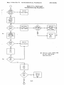
6. TROUBLESHOOTING PROCEDURES
6.1. Tools Required
6.2. Troubleshooting Flowchart
6.3. Measuring Power Supply Voltages
6.4. Tips on Troubleshooting Power Supply Problems
6-1
6-1
6-1
6-5
6-5
7. REPLACEMENT PARTS
7-1
8. CUSTOMER SERVICE BULLETIN INDEX
8-1
LIST
OF
F I G U R E S
X
2-1:
2-2:
2-3:
2-4:
2-5:
2-6:
2-7:
Revision A Chassis
Revision B Chassis
Revision C Chassis
Cover Removal - Revision A Chassis
Location of Screws - Revision A Chassis
Location of Screws - Revision B Chassis
Location of Screws - Revision C Chassis
2-1
2-1
2-2
2-3
2-3
2-4
2-5
3-1:
3-2A:
3-2B:
3-3:
3-4A:
3-4B:
3-4C:
MD I/MD II Drive Removal - Revision A Chassis
MD I/MD III Drive Removal - Revision B and C Chassis...
MD I/MD III Drive Removal - Revision B and C Chassis...
Separating MD III Drives - Revision B and C Chassis....
MD II- Revision B and C Chassis - Drive Removal
MD II- Revision B and C Chassis - Drive Removal
MD II- Revision B and C Chassis - Drive Removal
3-2
3-3
3-3
3-4
3-5
3-5
3-6
4-1:
Power- Supply Removal
5-1: Micro Decision Rev 1.1 Motherboard
5-2: Rev 2.0 Motherb6ard - Kohjinsha
5-3: Rev 2.0 Motherboard - Korean Assembled
5-4: Serial Port Pin Arrangement - Rear View
5-5: Factory Jumper Settings for JPA
5-6: JPA Settings for Modems
5-7: Jumper Settings (Pin 2 to Pin 2, Pin 3 to Pin 3)
5-8: Factory Jumper Settings for JPB
5-9: JPB Jumper Settings (Crisscross Modem Cable)
5-10: Alternate JPB Jumper Settings
5-11: Drive Expansion
4-2 ,t
5-1
5-5
5-6
5-8
5-10 ,-:'
5-11
5-11
5-13
5-14
5-14
5-19
LIST
OF
T A B L E S
5-1:
5-2:
5-3:
5-4:
5-5:
5-6:
5-7:
5-8:
5-9:
5-10:
5-11:
5-12:
5-13:
5-14:
Micro Decision Rev 1.1 Port Addresses
5-2
Rev 1.1 Bit Map (RAM Location)
5-2
Micro Decision Revision 2.0 Port Addresses
5-4
Rev 2.0/Kohj insha Bit Map (RAM Location)
5-5
Rev 2.0/Korean Assembled Bit Map (RAM Location)
5-6
Parallel Port Addresses
5-7
Parallel Port Signals (Kohjinsha Rev 2.0 Board)
5-7
Parallel Port Signals (Korean Assembled Rev 2.0 Board). 5-8
RS-232 Signal Descriptions
5-9
JPA Pinouts (Terminal Setup)
5-10
JPB Pinouts (Terminal Setup)
5-12
Sample RS-232 Cable Configurations
5-15
40 Pin I/O Connector - Pin Connections
5-16
Disk Drive Connectors - Pin Connections
5-20
6-1:
Troubleshooting Flowchart
6-2
7-1:
7-2:
Replacement Parts List
Dealer Service Kit
7-1
7-2
Part I-Section 1: Tools Required for Disassembly
1.
(09/23/83)
TOOLS REQUIRED FOR DISASSEMBLY
You will need a Phillips screwdriver, preferably size #2 and
magnetic.
Keep any magnetized tools away from diskettes that
contain valuable files.
To help insure against callbacks, you should wear a grounding
wriststrap that is connected to the Micro Decision
chassis
whenever you handle the mother board.
1-1
Part I-Section 2: Cover Removal
2.
(09/23/83)
COVER REMOVAL
Before removing the cover, turn off the Micro Decision and unplug
the equipment from the ac power source.
Failure to do so presents a serious hazard to the equipment and to service personnel.
Next, disconnect all cables from the rear of the unit.
At this printing, Morrow has installed three versions of Micro
Decision chassis.
For clarification, we refer to them as Revision A (original model), Revision B, and Revision C (newest
chassis style).
The simplest way to distinguish the three chassis revisions is to
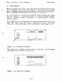
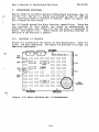
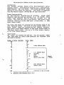
view the unit from the rear.
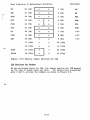
Revision A has a cord pan
installed, and the AC power cord is hardwired (see Figure 2-1).
and the power
Figure
2-2: Revision B Chassis
2-1
Part I-Section 2: Cover Removal
(09/23/83)
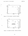
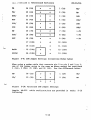
The third chassis style (Revision C) is similar to the Revision B
chassis, but can be identified by the knockout provided on the
rear panel for a fan.
The fan is installed in MD XI units only.
Another distinguishing characteristic is the location of the
drive expansion knockout.
It is located in the upper right
portion of the Revision C rear panel, rather than at the base.
The Revision C chassis also has two screws provided for removal
of the Micro Decision motherboard.
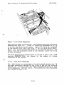
FAN KNOCKOUT
MOTHERBOARD
REMOVAL
Figure
2.1.
DRIVE
EXPANSION
KNOCKOUT
2-3: Revision C Chassis
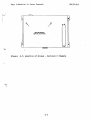
Revision A Chassis
1.
Remove the four screws on the bottom that hold the cover
to the chassis (see Figure 2-4).
2.
Now remove the two screws at the upper corners of
unit's back that hold the cover to the back panel.
the
3.
Carefully remove the cover by sliding it off towards
front.
the
2-2
Figure
2-5: Location of Screws - Revision A Chassis
2-3
(09/23/83)
Part I-Section 2: Cover Removal
2.2.
Revision B and C Chassis
1.
Remove the four
either side).
NOTE:
screws closest to the
edge
A magnetized screwdriver is not required
working on Revision B and C chassis.
2.
Tip the unit and rest it on the rear panel.
3.
Slide the cover up and off.
Figure
(two
2-6: Location of Screws - Revision B Chassis
2-4
on
when
Part I-Section 2: Cover Removal
Figure
(09/23/83)
2-7: Location of Screws - Revision C Chassis
2-5
Part I-Section 3: Disk Drive Configuration and Removal (09/23/83)
3.
DISK DRIVE CONFIGURATION AND REMOVAL
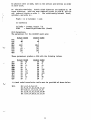
There are three drive configurations for the Micro Decision:
MD
MD
I - One 3/4 high, single sided, 5 1/4 inch floppy
drive, mounted at the left (as you face the unit)
II - Two 3/4 high, single sided,
drives, mounted side by side
5 1/4
inch
floppy
MD III - Two 1/2 high, double sided floppy drives, stacked
(drive B mounted above drive A) in the left half
of the unit (as you face the front)
Drive removal depends on the configuration of the drives and the
type of chassis in which these drives are installed.
NOTE:
3.1.
When removing MD II or MD III drives from a Revision 1.1
motherboard, it is very important that you mark disk
drives as A or B, since they must go back in the same
positions from which they came.
The best method is to
place a piece of masking tape on the B drive with a note
"next to power supply".
MD I and MD II - Revision A Chassis
1.
Turn the unit upside down and remove the three screws
that anchor the drive you wish to remove.
Figure 3-1
points out the positions of the screws for both drives.
2.
While holding the loosened drive in place, turn the unit
right side up.
Disconnect the drive cable and carefully
pull it backwards out of the chassis.
3-1
Fart l-Section 3: Disk Drive Configuration and Removal (09/23/83)
3.2.
MD III - Revision A Chassis
1.
Follow the instructions provided for MD I and MD II drive
removal (Section 3.1).
2.
Remove the strap which holds the two drives together.
Remember to mark one or both of the drives; drive B must
be reinstalled on top of drive A.
3.3.
MD I and MD III - Revision B and C Chassis
1.
Disconnect the flat ribbon cable (s) from the connector(s)
on the drive(s).
Then disconnect the cable(s) to the
motherboard.
For MD III configurations, we recommend
that you mark the cables for drive B to identify them
when reinstalling the drive.
2.
Remove the two bottom
left (see Figure 3-2A).
screws from the brackets on
3-2
the
Part I-Section 3: Disk Drive Configuration and Removal (09/23/83)
Figure 3-2A: MD I/MD III Drive Removal - Revision B and C Chassis
3.
Remove the screw at the base of the "L" bracket on the
right side as viewed from the front of the unit (see
Figure 3-2B).
Figure 3-2B:
4.
MD I/MD III Drive Removal - Revision B and C Chassis
Slide the drive(s) toward the rear and out.
3-3
IJISK urive Configuration and Removal (09/23/83)
Figure
3.4.
3-3: Separating MD III Drives - Revision B and C Chassis
MD II - Revision B and C Chassis
1.
Remove the cable connectors from the drive you
remove.
2.
Remove the screw at the base of the bracket holding
two drives (see Figure 3-4A).
3-4
wish
to
the
Part I-Section 3: Disk Drive Configuration and Removal (09/23/83)
Figure
3-4A: MD II - Revision B and C Chassis - Drive Removal
a. If removing the A drive, remove the two screws
the support bracket (see Figure 3-4B).
on
Figure 3-4B: MD II - Revision B and C Chassis - Drive Removal
b. If removing the B drive, you must first remove the
power supply (see Section 4), and then unscrew the
support bracket.
3-5
Part I-Section 3: Disk Drive Configuration and Removal (09/23/83)
3.
Toggle the "L" bracket connected to the drive as shown in
Figure 3-4C.
Figure 3-4C: MD II - Revision B and C Chassis - Drive Removal
4.
Carefully pull the drive toward the rear of the unit.
3-6
Part I-Section 4: Power Supply Removal
4.
(09/23/83)
POWER SUPPLY REMOVAL
The location of screws used to remove the power supply is identical for all chassis revisions. Figure 4-1 shows the Revision B
chassis, but can also be used as reference for Revision A and
Revision C power supply removal.
Procedures for power supply removal, which are dependent on the
type of chassis being serviced, are documented below.
4.1.
Revision A Chassis
1.
If removing the power supply from an MD II,
drive as described in Section 3.1.
2.
Disconnect the power supply harness from the mother board
and the cable that powers the LED in the Reset switch.
3.
With the unit upside down, remove the four screws on
either side of the power supply's ventilation grill
(see
Figure 4-1). The power supply will drop lightly onto the
benclf.
4.
When installing the new power supply, route its wires as
far away from drive B as possible. Make sure you do not
pinch any wires between the power supply and the chassis.
4.2.
remove the B
Revision B and C Chassis
1.
With the unit upside down, remove the four screws on the
either side of the power supply's ventilation grill
(see
Figure 4-1). The power supply will drop lightly onto the
bench.
2.
If removing the power supply from an MD II,
drive as described in Section 3.4.
3.
Disconnect the power supply harness from the mother board
and the cable that powers the LED in the Reset switch.
4.
When installing the new power supply, route its wires as
far away from drive B as possible.
Make sure you do not
pinch any wires between the power supply and the chassis.
4-1
remove the B
x-oecrion 4: Power Supply Removal
(09/23/83)
Figure
4-1: Power Supply Removal
4-2
Part I-Section 5: Motherboard Revisions
5.
(09/23/83)
MOTHERBOARD REVISIONS
Morrow supports two Micro Decision Motherboard revisions: Rev 1.1
and Rev 2.0. The Rev 1.1 boards were phased out May 21, 1983 and
are generally found in Revision A chassis. Refer to Figure 5-1
for a layout of this board.
Rev 2.0 boards expand the Micro Decision capabilities. There are
two versions of this board; one board is manufactured by
Kohjinsha in Japan (see Figure 5-2) and the other is assembled in
Korea (see Figure 5-3).
These boards are generally mounted in
Revision B and Revision C chassis.
5.1.
Revision 1.1 Details
Figure 5-1 illustrates the layout of this motherboard. Table 5-1
lists the port addresses, and Table 5-2 provides a bit map for
RAM chip replacement.
Figure
5-1: Micro Decision Rev 1.1 Motherboard
5-1
rare i-section b: Motherboard Revisions
(09/23/83)
Table 5-1: Micro Decision Rev 1.1 Port Addresses
PORT
FUNCTION
OF5
MOTOR CHECK PORT
OF6
ROM ENABLE/DISABLE
(out=enable/in=di sable)
OF 7
VFO COUNT SET PORT
OF 8
MOTOR & SHIFT CONTROL
OFA
UPD-765 STATUS
OFB
UPD-765 DATA
OFC
1st. SERIAL PORT DATA
OFD
1st. SERIAL PORT STATUS
OFE
2nd. SERIAL PORT DATA
OFF
2nd. SERIAL PORT STATUS
Table 5-2: Rev 1.1 Bit Map (RAM Location)
BIT
LOCATION
0
9G
1
8G
2
9H
3
8H
4
9J
5
8J
6
9K
7
8K
5-2
Part I-Section 5: Motherboard Revisions
5.2.
(09/23/83)
Motherboard Removal
CAUTION!
When handling motherboards, you should take care to
avoid damage to them through electrostatic discharge.
Ideally you should wear a grounded wriststrap, but we
doubt you will; so at least moisten carpets with a
spray bottle and discharge yourself by touching the
Micro Decision chassis frequently as you work.
Handle
the board by the edges, and avoid touching 1C leads or
solder connections.
1.
Remove both disk drives as described above.
2.
Disconnect all cables from the motherboard. You will not
be able to disconnect the ribbon cables leading to the
disk drives, as they are glued to the motherboard and are
replaced along with the board.
3.
If the unit has a cord pan (rectangular box) attached to
the inside of the back panel, remove it by removing the
four screws that secure it to the back panel.
4.
Rest the unit on its side. If disassembling a Revision A
or Revision B chassis, remove the four screws on the
bottom that hold the motherboard to the chassis
(see
Figure 2-5 or 2-6). If working with a Revision C chassis,
remove the two screws on the bottom and the two screws on
the rear panel which secure the motherboard (see Figure
2-3 and Figure 2-7).
Support the board with your hand
(do NOT push hard against it) when you remove the last
screw, to keep it from falling.
5.
Put the unit back on its bottom.
Slide the motherboard
toward the front of the chassis until the peripheral
cable connectors
are on the inside of their cutouts.
Then gently lift the board out by its rear end, sliding
it away from the front of the chassis as you go.
5.3.
Revision 2.0 Features
The Micro Decision Rev 2.0 board differs with the Rev 1.0
in several aspects:
board
1.
The addition of a Centronics compatible parallel port.
2.
Software selectable baud rate generator (Intel 8253).
3.
40 pin I/O connector
4.
Internal
board.
5.
Improved floppy disk data separator.
(for future enhancements).
ROM diagnostics for testing the function of the
5-3
Part I-Section 5: Motherboard Revisions
(09/23/83)
The new Rev 2.0 board will not effectively run CP/M with a Morrow
revision lower than 2.1. The Rev 1.0 board will not run CP/M with
a Morrow revision greater than Rev 1.6.
External disk drives (C and D) are now "daisy-chained" from drive
"B" since the parallel connector is located where the drive
expansion connector was on the Rev 1.1 board.
External drives
are also configured differently for the Rev 2.0 board.
The Micro Decision uses two different Rev 2.0 board layouts. One
board is manufactured by Kohjinsha Inc.
It can be identified by
the Kohjinsha label located to the right of the board near the
power plugs (PJ1-PJ3) on the component side.
The jumper for the
diagnostics is labeled JP4, and is at location A-5, 6.
The 40
pin I/O connector is at location F-l thru K-l.
Refer to Figure
5-2 for a diagram of this board.
The second board can be identified by the "ASSEMBLED IN KOREA"
label located to the right of the board near the power supply.
Also,
the power connectors (PJl) are located differently,
location A, B-8.
The jumper for the diagnostics is labeled E5,
and is at- location A-6, 7.
The 40 pin I/O connector is at
location A-6, 7 thru D-6, 7. Figure 5-3 illustrates the layout
of this board.
The two boards are functionally identical. Port addresses, which
apply to both layouts, are listed in Table 5-3.
Table 5-3: Micro Decision Revision 2.0 Port Addresses
All other ports remain the same as Rev 1.1 (see Table 5-1)
5-4
Figure
5-2: Rev 2.0 Motherboard - Kohjinsha
f~
Table 5-4: Rev 2.0/Kohjinsha Bit Map (RAM Location)
BIT
RAM LOCATION
0
8J
1
8J/K
2
8K
3
8L
4
9J
5
9J/K
6
9K
7
9L
5-5
5-6
Part I-Section 5: Motherboard Revisions
5.3.1.
(09/23/83)
Parallel Port
The Micro Decision's unidirectional parallel port is a Centronics
compatible port employing a 34 pin edge connector for connection
to a printer.
The data is transferred through a 74LS374 tristate buffer to the connector.
The addresses for the ports are
listed in Table 5-6.
Table 5-6: Parallel Port Addresses
F4
F5
Data port
Status port
Read: bit 3 = 1=ACK
bit 4 = l=Busy
Write: bit 7 = Strobe
The signals for the 34 pin edge connector are listed in Table 5-7
(Rev 2.0 Kohjinsha) and Table 5-8 (Korean-assembled Rev 2.0
board).
Table 5-7: Parallel Port Signals (Kohjinsha Rev 2.0 Board)
PIN
SIGNAL
1
3
5
7
9
11
13
15
17
19
21
STROBE
DBO
(neg.)
DB1
DB2
DB3
DB4
DBS
DB6
DB7
Acknowledge
Ready/Busy
(neg.)
Even pins 2-24, 34 twisted pair ground; all other pins n/c
5-7
rare i-section 5: Motherboard Revisions
(09/23/83)
Table 5-8: Parallel Port Signals (Korean Assembled Rev 2.0 Board)
PIN
2
4
6
8
10
12
14
16
18
20
22
SIGNAL
STROBE
(neg.)
DBO
DBl
DB2
DB3
DB4
DBS
DB6
DB7
Acknowledge (neg.)
Ready/Busy
Odd pins 1 - 2 3 , 33 twisted pair ground; all other pins n/c
The SETUP program on the CP/M diskette must be used to set
CP/M LST device to acknowledge the parallel port instead of
second serial port.
the
the
Special Notes:
If the terminal used with the Micro Decision will not operate at
9600 baud, you must run SETUP using the CP/M distribution diskette to create a system diskette first.
When you do this, don't be surprised when "garbage" appears on
the screen each time you press the reset button.
This is a
garbled version of the message that normally tells you to insert
the CP/M diskette and press Return. It is sent out at 9600 baud,
so the installed terminal misinterprets it.
After you press
Return, however, the new baud rate takes over and everything
proceeds normally from there.
5.3.2.
Serial Ports
The serial connectors on the Micro Decision motherboard conform
to RS-232 standards, and use DB 25/S connectors.
Figure 5-4
shows the layout of the connector, and Table 5-9 identifies the
signal associated with each of the pins.
Left
Figure
5-4: Serial Port Pin Arrangement - Rear View
5-8
(09/23/83)
Part I-Section 5: Motherboard Revisions
Table 5-9: RS-232 Signal Descriptions
Pin f
1
2
3
4
5
6
7
8
9
10
11
14
17
20
24
These
only.
Signal
*
*
*
*
*
*
Frame Ground
Receive Data Input
Transmit Data Output
Request to Send Input
Clear To Send Output
Data Set Ready Output
Signal Ground
Carrier Detect Output
+12V Output
-12V Output
Alternate Handshake Line
+5V Output
Receiver Clock Output
Data Terminal Ready Input
Transmitter Clock Input
signals are available on the
printer/modem
connector
On the circuit board in front of each serial connector is a set
of jumper headers labelled JPA and JPB.
JPA has eight pairs of
jumpers for defining the terminal port; JPB has 13 pairs that
define the printer/modem port.
Slip-on connectors are used to
make the RS-232 pin assignments. By changing the positions of
some connectors, the ports can be configured for use with modems.
The jumpers select whether the serial connector is set up to talk
to DCE or DTE equipment.
JPA Factory Settings
The terminal port can be configured for DCE. The signal present
on each jumper pin in JPA is shown in Table 5-10, along with the
factory setting for the feeding of the signals to the RS-232
connector.
The reason the pin numbers appear as 1 (1A) is that
the board may be silkscreened in either of these two ways.
5-9
Part I-Section 5: Motherboard Revisions
Table 5-10:
JPA Pin *
1
2
3
4
5
6
7
8
9
10
11
12
13
14
15
16
(1A)
(2A)
(3A)
(4A)
(5A)
(6A)
(7A)
(8A)
(8B)
(7B)
(6B)
(5B)
(4B)
(3B)
(2B)
(IB)
(09/23/83)
JPA Pinouts (Terminal Setup)
Signal
RxD to UART
RD to terminal
L/SR to terminal
DSR/ to UART
DTR from terminal
DTR/ from UART
+12V
+12V
CTS/ to UART
CD from terminal
CTS to terminal
CTS/ to UART
RTS from terminal
RTS/ from UART
TxD from UART
TD from terminal
RS-232 Pin f
I
3
6
4
N/C
5
9
8
8
8
5
8
4
€
3
2
This signal configuration is accomplished through circuit board
wiring and the factory jumper settings, as shown in Figure 5-5.
When setting up JPA for use with a modem on the terminal port,
the jumper modifications depend on whether the modem cable has
pin 2 at one end tied to pin 3 at the other, and vice versa.
This crisscrossing is frequently, but not always, found in modem
cables.
If you're not sure which type you have, use an ohmmeter
or continuity tester to find out.
RD/
RD
DSR
DSR/
DTR
DTR/
+12V
+12V
5-10
rare i-section 5: Motherboard Revisions
(09/23/83)
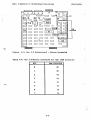
JPA Settings for Modems
For cables that crisscross pins- 2 and 3,
shown below.
Figure
arrange the jumpers
as
5-7: Jumper Settings (Pin 2 to Pin 2, Pin 3 to Pin 3)
Factory Settings for JPB
The printer/modem port would be configured for a modem if you
want to use the Micro Decision as a host computer
contacting
remote computers or data bases.
5-11
(09/23/83)
The signal present on each
11, along with the factory
to the RS-232 connector.
(1A) is that the board may
ways.
jumper pin in JPB is shown in Table 5setting for the feeding of the signals
The reason the pin numbers appear as 1
be silkscreened in either of these two
Table 5-11: JPB Pinouts (Terminal Setup)
JPA Pin 1
1
2
3
4
5
6
7
8
9
10
11
12
13
14
15
16
17
18
19
20
21
22
23
24
25
26
(1A)
(2A)
(3A)
(4A)
(5A)
(6A)
(7A)
(8A)
(9A)
(10A)
(11A)
(12A)
(13A)
(13B)
(12B)
(11B)
(10B)
(9B)
(8B)
(7B)
(6B)
(5B)
(4B)
(3B)
(2B)
(IB)
Signal
RxD to UART
RD to terminal
DSR to terminal
DSR/ to UART
DTR from terminal
DTR/ from UART
TTL false (<-3V)
TTL false
TTL false
Receiver Clock to modem
RS-232 Receiver input
TTL output of RS-232 rcvr
N/C
Baud Clock output
Baud Clock input to UART
TC (External Clock)
RS-232 level clock out
DET (alternate handshake)
GTS/ to UART
CD from terminal
CTS to terminal
CTS/ to UART
RTS from terminal
RTS/ from UART
TxD from UART
TD from terminal
RS-232 Pin #
2
3
6
20
20
5
8
8
8
17
N/C
N/C
N/C
N/C
24
N/C
11
8
8
5
8
4
6
3
2
This signal configuration is accomplished through circuit board
wiring and the factory jumper settings as shown in Figure 5-8.
5-12
r
Figure
5-8: Factory Jumper Settings for JPB
JPB Settings for Modems
As was mentioned above for JPA, the jumper setting for JPB depend
on the type of modem cable you have.
For cables that crisscross
pins 2 and 3, arrange the jumpers as shown in Figure 5-9.
5-13
(09/23/83)
^
5-14
Part I-Section 5: Motherboard Revisions
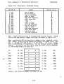
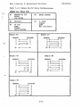
Table 5-12: Sample RS-232 Cable Configurations
LEGEND for Table 5-9:
(09/23/83)
Part I-Section 5: Motherboard Revisions
5.3.3.
40 Pin I/O Connector
5-16
(09/23/83)
Part I-Section 5: Motherboard Revisions
5.3.4.
(09/23/83)
ROM Diagnostics
The Micro Decision Rev 2.0 board has diagnostic routines built
into the 4K ROM.
To access the diagnostics, locate the jumper
labeled JP4 or E5.
Install a jumper block at that location and
turn on the computer.
If the power-on memory test passes, the
following should appear on the screen:
1.
2.
3.
4.
5.
6.
7.
8.
9.
PORT 1
\
PORT 2
>
CENTRONICS PORT
/
LOOP BACK ON PORT 2
RAM TEST
FDC R/W
FDC SEEKTEST
VFO TEST
BOOT
Enter #:
BARBER-POLE TEST PATTERN
'
:.
Description of Test:
-/
NOTE:
1.
To end a test, press any key and wait for the Diagnostics
Menu to reappear.
Port 1 test:
This test transmits a "barber-pole" character pattern
the CRT.
2.
Port
2
test:
This test transmits a "barber-pole" character pattern
the device connected to serial port 2.
3.
to
Centronics
port
to
test:
This test transmits a "barber-pole" character pattern to a
printer via the Centronics parallel port.
.
4.
Loop
back
on port 2 test:
This test verifies proper operation of the 8251 USART on
port 2. A wrap plug with pins 2 and 3 jumpered and pins 5
and 20 jumpered must be used.
This test will immediately
show pass or fail.
5.
Ram
Test:
This test runs a continuous ram test.
The test will show
any address which is found to be bad, the value expected
and the value read from the bad address.
5-17
D: nocnerooard Revisions
6.
(09/23/83)
FDC (Floppy Disk Controller) Read/Write test:
This test performs a "worst case" read/write test on
inner most track of a diskette, reporting errors to
screen. A freshly formatted diskette should be used.
7.
FDC
the
the
Seektest:
This test will perform a butterfly seektest
(outermost
track to innermost track, working inward to center, and
then back out again) on a selected disk drive.
8.
VFO
(Variable Frequency Oscillator)
test:
This test is used for verifying the proper operation of
the PLL data separators.
A frequency counter and a known
good Shugart SA200 disk drive is required to perform this
test.
The SA200 disk drive must be installed as drive
"A".
Connect the lead of the frequency counter to the
test point labeled VCOTP, at location E-l on the Kohjinsha
board, or the test point location labeled TPl on the
Korean assembled board.
Insert a formatted diskette in
drive "A", close the door and select the VFO Test from the
menu.
Open the disk drive door and read the frequency.
The frequency should read 480Khz ±30Khz on the Kohjinsha
board, or 500 Khz +.30Khz on the Korean assembled board.
Ignore intermittent fluctuations in frequency of greater
than 10 Khz.
9.
Boot:
Selecting item 9 will cause the system to boot a diskette
in drive "A".
Remember to remove jumper block after completing diagnostics.
5.3.5.
Drive Expansion
External disk drives (C and D) are "daisy-chained" from drive
"B".
When external drives are added to an MD II or MD III, the
current 34 pin ribbon data cable must be removed and a new ribbon
cable must be installed in its place (see Figure 5-11). This new
cable consists of two edge connectors and one 2 X 16 header plug.
One of the edge connectors is connected to drive B, and the other
is connected to the motherboard (see Section 5.3.6, Disk Drive
Connector). The header plug must be installed in the rear of the
chassis where the "knockout" plug is located (directly above the
parallel port). The cable supplied with the external drive is an
identical mating cable.
5-18
Part I-Section 5: Motherboard Revisions
Figure
(09/23/83)
5-11: Drive Expansion
Once the new cable is installed, the termination block should be
removed^from drive "B".
Drive "D" should be terminated if it is
to be the last drive on the chain.
Drive "C" is to be selected
as the second drive (DS2) and drive "D" as the third drive (DS3).
Drive "C" is not terminated unless it is the last drive on the
chain, then the terminator block is not removed. Drive "A" is to
be left unchanged.
The CP/M distribution diskette must be booted to make a new CP/M
working diskette with the change in the number of drives
installed on the system.
5.3.6.
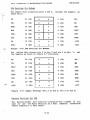
Disk Drive Connector
The disk drives are connected to the motherboard through two 34
pin edge connectors labeled JDO for drive A, and JDl for drives B
through D.
Drives C and D are daisy-chained from drive B (see
Drive Expansion, Section 5.3.5). The pinouts for the connectors
are listed in Table 5-14.
5-19
Part I-Section 5: Motherboard Revisions
(09/23/83)
Table 5-14: Disk Drive Connectors - Pin Connections
JDO
JDl
8
/INDEX
8
/INDEX
10
/DSO
10
/DSO
16
/MOTOR
12
/DS1
18
/DIRECTION
14
/DS2
20
/STEP
16
/MOTOR
22
/WRITE DATA
18
/DIRECTION
24
/WRITE GATE
20
/STEP
26
/TRACK 0
22
/WRITE DATA
28
/WRITE PROTECT
24
/WRITE GATE
30
/READ DATA
26
/TRACK 0
32
/SIDE SELECT
28
/WRITE PROTECT
30
/READ DATA
32
/SIDE SELECT
All odd numbered pins on JDO and JDl are grounded.
5-20
Part I-Section 6:
6.
I
6.1.
Troubleshooting Procedures
(09/23/83)
TROUBLESHOOTING PROCEDURES
Tools Required
You will need the Phillips screwdriver, the Diagnostic II
diskette, and a digital voltmeter. The meter (Kiethley model 132
or equivalent) is needed when the power supply is suspect, and is
also useful for checking the continuity of cables.
Another
helpful device is a floppy diskette head cleaning kit.
6.2.
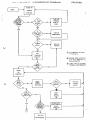
Troubleshooting Flowchart
Use the troubleshooting flowchart (see Table 6-1) for isolating a
defective assembly within the Micro Decision, as well as for
determining whether the trouble lies outside the computer (in
cables or peripherals, for example).
Follow the procedure as
described in the figure. .
If you find that the problem lies somewhere in the Micro
Decision, you will be instructed to run the diskette diagnostic
programs.
You will need the Diagnostics II diskette and a
terminal known to be working properly.
6-1
Part I-Section 6:
6.3.
_,/
\ .
Troubleshooting
Procedures
(09/23/83)
Measuring Power Supply Voltages
If you reach the point in the troubleshooting flowchart that
tells you to "check power supply voltages", here is what you do:
1.
With the power cord unplugged, remove the cover as
described in Section 2.
Then reconnect the power cord
and turn the power switch ON.
2.
Connect the ground lead (probably black) from the voltmeter to an exposed metal part of the chassis
(preferably a drive). Use an alligator clip for best results.
3.
Locate connector PJ3 on the motherboard, next to the
power supply. Make sure your meter is set up to measure
volts on the other meter probe into pin 1 (the red cable
lead). You should measure +5 volts.
4.
At pin 4 (the blue lead), the +12 volts that powers the
disk drive motors should be present.
5.
To check the + and -12 volts to Rev 2.0 motherboard circuitry, use the 40 pin I/O connector on the board:
+5v
+12v
-12v
Pins 38 and 40
Pin 36
Pin 34
Voltage (+5v and +12v) to the Rev 1.1 boards can be
checked from the disk drives.
-12 volts can be checked
from the 1488 serial buffer at location A-l.
_6.
If any or all of the voltages are missing, or if they
vary from the specified voltage by more than 10%, the
power supply should be replaced.
Refer to Section 4,
"Power Supply Removal" for instructions.
However, this
may not fix the problem (see Tips below).
7.
Recheck the voltages even if the problem is cleared up;
this is to be sure that nothing is putting too much of a
load on the power supply.
6.4.
Tips on Troubleshooting Power Supply Problems
A voltage that is lower than it should be could be caused by
leakage or shorts outside of the power supply itself.
Assuming
that you have already substituted the power
supply,
try
disconnecting the disk drives one at a time and rechecking the
voltages as you go. If you get down to just the power supply and
motherboard being connected and the voltage is still low, then
replace the motherboard.
6-5
(09/23/83)
Part I-Section 7: Replacement Parts
7.
REPLACEMENT PARTS
Table 7-1: Replacement Parts List
PART NO.
DESCRIPTION
020-SA455
SA455
020-F5200
SA200
A. INSERT BRKT
125-MHLED
B. LED HARNESS
028-LED3105
080-MFP
500-PCBM-Rev 1.1
or Rev 2.0
1.
B.
LED (3 PC)
FRONT PANEL
ASSM PCB (REPRO ROM)
060-34122C
A.
CABLE 34S 12"
102-SPM
B.
STAND-OFF
125-MHDC
C.
DC POWER CABLES
500-SWPSM
POWER SUPPLY
125-MHRESET
RESET HARNESS
096-06X14PST
SCREW (632 TYP "F")
096-3X6M-PP
SCREW 3X6MM PAN PHIL
The Dealer Service Kit follows in Table 7-2.
7-1
Part I-Section 7: Replacement Parts
(09/23/83)
Table 7-2: Dealer Service Kit
(Effective Date: October 1, 1983)
Above prices are NOT discountable.
All parts carry Morrow's factory warranty of 30 days
from date of purchase.
Remedy is limited to repair or
replacement of the defective part at the option of
Morrow.
Parts supplied are reconditioned and are not
to be resold as new.
In any case, Morrow will not be
liable for consequential damages arising from the use
of its products.
Prices supersede those published June 1, 1983 in Dealer
Information Bulletin #5.
Prices are subject to chang
without notice.
To order kits, please contact Customer Service.
A
maximum of one (1) service kit may be purchased for
each 10 systems.
7-2
Part I-Section 8: Customer Service Bulletin Index
8.
(09/23/83)
CUSTOMER SERVICE BULLETIN INDEX
BULL.
£
DATE
SUBJECT
ISSUED BY
1
Nov. 82
Micro Decision
1.3 PROM/Software
T. Fruehan
2
Nov. 82
Micro Decision
Power Supply Upgrade
T. Fruehan
3
Dec. 82
Micro Decision
Software Remake
T. Fruehan
4
OBSOLETE
5
OBSOLETE
6
Feb. 83
MDT20 Terminal
Terminal PROMs
7
Mar. 83
MDT50 Terminal
Terminal Service
8
Mar. 83
Micro Decision
Printer Port Info
9
Mar. 83
MDT20 Terminal
Terminal Service
10
Apr. 83
MDT20 Terminal
Terminal Mod.
T. Fruehan
11
Apr. 83
Micro Decision
Terminal Configuration
T. Fruehan
12
T. Fruehan
J. Patel
T. Fruehan
J. Patel
Cancelled
12-A
May
83
MP100, MP200, MP300
Printer Service
13
May
83
Micro Decision
Rev 2.0 Board Release
T. Fruehan
14
May
83
DJDMA Board
S-100 Bus Standards
N. Tilbury
Cancelled
15
16
M. Dean
Jun. 83
Quest Software
Software Support
8-1
T. Fruehan
; ^uscomer service Bulletin Index
17
Jun. 83
T. Fruehj
Cancelled
18
19
Micro Decision
Software Upgrade
(09/23/83)
Jul. 83
Micro Decision
PROM/Software Upgrade
R. Rowe
Cancelled
20
21
Aug. 83
MDT 20 Terminal
Terminal Service
M. Dean
22
Aug. 83
Micro Decision
Printer Patch
L. Hamel
23
Sep. 83
Decision One
Software Upgrade
W. Bingr
24
Sep. 83
Decision One
Micronix
W. Bingfc
8-2
Morrow Micro
Decision
Board
Revision 2.0 Technical Information
Supplement
PARALLEL PORT
The Micro Decision's parallel port is a Centronics compatible
port employing a 34 pin edge connector for connection to a
printer. The data is transferred through a 74LS374 tri-state
buffer to the connector. The addresses for the ports are:
F4
P5
Data port
Status port
Reads bit 3 » 1«ACK
bit 4 « l«Busy
Write: bit 7 - Strobe
The signals for the 34 pin edge connector are:
Odd pins 1 - 23/33
2
4
6
-8
10
12
14
16
18
20
22
All other pins n/c.
twisted pair ground- .
STROBE
(neg.)
DBO
DB1
DB2
DB3
DB4
DBS
DB6
DB7
Acknowledge (neg.)
Ready/Busy
The SETUP program on the CP/K diskette must be used to set the
CP/M LST device to acknowledge the parallel port instead of the
second serial port.
PORT
FUNCTION
OF5
MOTOR CHECK PORT
OF6
OF7
ROM ENABLE/DISABLE
(out»enable/in«disable)
VFO COUNT SET PORT
OPE
MOTOR & SHIFT CONTROL
OFA
UPD-765 STATUS
OFB
UPD-765 DATA
OFC~
1st. SERIAL PORT DATA
OFD
1st. SERIAL PORT STATUS
OFE
2nd. SERIAL PORT DATA
OFF
2nd. SERIAL PORT STATUS
MICRO DECISION REVISION 2.0 PORT ADDRESSES
OFO
OF1
OF2
OF3
8253
BAUD RATE GENERATOR
OF4
CENTRONICS DATA PORT
»OF5
CENTRONICS STATUS PORT
read bit 3 ACK-1
write bit 7 stobe-0
read bit 4 busy-1
t
All other ports remain the sane.
mdporttf
40 PIN I/O CONNECTOR
BAUD RATE GENERATOR
The baud rates for the Micro Decision are s o f t w a r e selectable
t h r o u g h t h e S E T U P p r o g r a r r . T h e b a u d r a t e g e n e r a t o r is a n I n t e l
8253 counter t i m e r chip which is accessed through ports OPO-OF3h
C h a n n e l 0 is u s e d for Floppy Drive T i m i n g and s h o u l d not be
w r i t t e n to;
C h a n n e l 1 is serial port 1 ba"udT Channel^ Ts
serial port 2 baud.
The seven m o s t p o p u l a r b a u d r a t e s (110, 3 0 0 , 6 0 0 , 1200, 2 4 0 0 ,
4 8 0 0 and 9 6 0 0 ) can be chosen through the SETUP p r o g r a m for both
serial ports.
The SETOP p r o g r a m a l s o e n a b l e s you to choose
between software h a n d s h a k i n g , (XON-XOFF) or h a r d w a r e handshakings
(DTR pin 20) on the second serial port.
DISK DRIVE CONNECTOR
The disk drives are connected to the motherboard through two 34
pin edge connectors labeled JDO for drive "A", and JD1 for drives
"B" through "D". Drives "C" and "D" are daisy-chained from drive
"B". The pin-outs for the connectors are listed below.
JDO
8
10
16
18
20
22
24
26
28
30
32
JD1
/INDEX
/DSO
/MOTOR
/DIRECTION .
/STEP
/WRITE DATA
/WRITE GATE
/TRACK 0
"V WRITE PROTECT
/READ DATA
/SIDE SELECT
8
10
12
14
16
18
20
22
24
- 26
28
30
32
/INDEX
/DSO
/DS1
/DS2
/MOTOR/DIRECTION
/STEP
/WRITE DATA
/WRITE GATE
/TRACK 0
/WRITE PROTECT
/READ DATA
/SIDE SELECT
All odd numbered pins on JDO and JD1 are grounded,
Micro-Decision Diskette Format Specifications.
Introduction:
This document provides details of the Micro-Decision's native
diskette format. Micro-Decision diskettes use a soft-sectored,
double-density, IBM like format. Both single and double sided
versions of this format are supported.
This format is compatible
with both Western Digital 179X and NEC 765 type controllers.
Format Characteristics:
All Micro-Decision diskettes have 40 cylinders.
Single sided
diskettes have one track per cylinder (i.e. 40 tracks), while
double sided diskettes have two tracks per cylinder (i.e. 80
tracks). Each track has five Ik byte sectors. This gives a total
formatted capacity of either 200k bytes (single sided) or 400k
bytes (double sided).
Two tracks (10k bytes) are allocated for the bootable image of the
CP/M operating system. And either 4k bytes (single sided) or 6k
bytes (double sided) are allocated for the diskette directory.
This gives a total usable capacity of 186k bytes (single sided) or
384k bytes (double sided), with up to 136 files (single density)
or 192 files (double density).
Track Format:
All tracks are formated the same way, only the cylinder number
(and head number for double sided diskettes) are different from
one track to another.
Number of Bytes (Decimal)
50—
12
3
1
50
12
3
1
1
1
1
1
2
22
12
3
1
1024
2
85
Value (Hex)
C2*
FC
4E
0
Al**
FE
0-27
0-1
1-5
3
C.R.C.
4E
0
Al**
FB
E5
C.R.C.
4E
Index Address Mark
I.D. Address Mark
Cylinder
Side
Sector
Sector Size Code
Repeat
5 Times
Data Address Mark
Default Data
Continue to end of track
"250
4E
* Missing clock between bits 4 & 5.
** Missing clock between bits 3 & 4.
No physical skew is used, that is the sectors are written in order
on each track.
On the Micro-Decision, double sided diskettes are handled as 80
track diskettes, with the even numbered tracks on side 0, and the
odd numbered tracks on side 1. The relationship between track,
cylinder, and side is :
Track = (2 x Cylinder) + side
or conversly
Cylinder = Integer (Track / 2)
Side
= Least-Significant-Bit (Track)
CP/M Parameters:
The parameters for the DISKDEF macro are:
Double Sided
1
40
*
2048
195
192
192
2
These parameters produce a DPB with the folowing values:
Single Sided
SPT
BSH
BI/1
EXM
DSM
DRM
AL0
AL1
CKS
OFF
DW
DB
DB
DB
DW
DW
DB
DB
DW
DW
Double Sided
40
4
15
1
94
127
192
0
32
2
* A hand coded translation table must be provided ad shown below:
XLT:
DB
DB
DB
DB
DB
1,2,3,4,5,6,7,8
25,26,27,28,29,30,31,32
9,10,11,12,13,14,15,16
33,34,35,36,37,38,39,40
17,18,19,20,21,22,23,24
Track 0 Data:
In order for the Micro-Decision to correctly access the diskette,
the following data MUST be on sectors 1 and 2 of track 0:
Data for track 0 sector 1 of single sided diskettes:
000D
CR
EQU 0DH
000A
0018
0003
LF
BTERR
MESG
EQU 0AH
EQU 18H
EQU 3
•
t
ORG 0FE00H
FE00
FE01
FE02
FE03
FE05
FE08
FE0B
FE0E
FE0F
FE10
FEU
FE12
FE15
FE16
FE17
FE1A
FE1C
FE1F
00
00
00
3E
32
CD
21
39
5E
23
56
21
19
EB
31
D3
CD
C3
FF00
F6
0003
0018
FE22
FE26
FE2A
FE2E
FE32
FE36
FE3A
0D
74
53
45
69
74
0D
0A
20
59
4D
73
74
0A
C9
FDFF
FDFF
FFFE
0017
,-
FE3D
FE80
FE82
FES 4
FES 6
FE88
FES 9
FE8B
FE8C
FE8D
FE8E
FE90
FE92
FE93
RADD:
4E
61
53
20
6B
65
00
6F
20
54
44
65
2E
EMSG:
MOP
NOP
NOP
LD A,0C9H
LD (0FDFFH),A
CALL 0FDFFH
LD HL,-2
ADD HL,SP
LD E, (HL)
INC HL
LD D, (HL)
LD HL,EMSG-RADD
ADD HL,DE
EX DE,HL
LD SP,0FF00H
OUT (0F6H),A
CALL MESG
JP BTERR
;JMP TO ROM
DB CR,LF,'Not a SYSTEM Diskette.
DB CR,LF,0
DS (0FE80H-$),0
0000
0000
0000
0000
00
0028
04
0F
01
005E
007F
C0
00
DW
DW
DW
DW
DB
DW
DB
DB
DB
DW
DW
DB
DB
0
0
0
0
0
40
4
15
1
94
127
0C0H
0
FE94
FE96
FE98
FE99
0020
0002
El
DW
DW
DB
DS
32
2
0E1H
103,0
Data for track 0 sector 1 of double sided diskettes:
000D
EQU 0DH
000 A
EQU 0AH
0018
EQU 18H
0003
EQU 3
ORG 0FE00H
FE00
FE01
FE02
FE03
FE05
FE08
FE0B
FE0E
FE0F
FE10
FEU
FE12
FE15
FE16
FE17
FE1A
FE1C
FE1F
FE22
FE26
FE2A
FE2E
FE32
FE36
FE3A
00
00
00
3E
32
CD
21
39
5E
C9
FDFF
FDFF
FFFE
23
56
21 0017
19
EB
31
D3
CD
C3
FF00
F6
0003
0018
0D
74
53
45
0A
20
59
4D
4E
61
53
20
6F
20
54
44
EMSG:
DB CR,LF,'Not a SYSTEM Diskette.'
69 73 6B 65
74 74 65 2E
0D 0A 00
FE3D
FE80
FE81
FE82
FE84
FE86
FES 8
FE89
FE8B
FE8C
FE8D
FE8E
FE90
NOP
NOP
NOP
ID A,0C9H
LD (0FEFFH),A
CALL 0FDFFH
LD HL,-2
ADD HL,SP
:
LD E,(HL)
INC HL
LD D,(HL)
LD HL,EMSG~PADD
ADD HL,DE
EX DE,HL '
LD SP,0FF00H
OUT (0F6H),A
CALL MESG
JP BTERR
;JMP TO ROM
DB CR,LF,0
DS (OFE80H-$),0
00
04
0000
0000
0000
00
0028
04
0F
01
00C2
00BF
DB
DB
DW
DW
DW
DB
DW
DB
DB
DB
DW
DW
0
4
0
0
0
0
40
4
15
01
194
191
FE92
FE93
FE94
FE96
FE98
FE99
E0
00
0030
0002
89
DB
DB
DW
DW
DB
DS
0E0H
0
48
2
89H
103,0
Data for track 0 sector 2 of single and double sided diskettes:
000D
CR
EQU 0DH
000A
0018
0003
LF
BTERR
MESG
EQU 0AH
EQU 18H
EQU 3
;
ORG 0FE00H
FE00
FE01
FE02
FE03
FE05
FE08
FE0B
FE0E
FE0F
FE10
FEU
FE12
FE15
FE16
FE17
FE1A
FE1C
FE1F
00
00
00
3E
32
CD
21
39
5E
23
56
21
19
EB
31
D3
CD
C3
FE22
FE26
FE2A
FE2E
FE32
FE36
FE3A
0D
74
53
45
69
74
0D
FE3D
C9
FDFF
FDFF
FFFE
RADD:
0017
FF00
F6
0003
0018
0A
20
59
4D
73
74
0A
4E
61
53
20
6B
65
00
6F
20
54
44
65
2E
EMSG:
NOP
MOP
NOP
LD A,0C9H
I£) (0FDFFH) ,A
CALL 0FDFFH
LD HL,-2
"'
ADD HL,SP
LD E,(HL)
INC HL
LD D,(HL)
LD HL,EMSG~RADD
ADD HL,DE
EX DE,HL
LD SP,0FF00H
OUT (OF6H),A
CALL MESG
JP BTERR
;JMP TO ROM
DB CR,LF,'Not a SYSTEM Diskette,
DB CR,LF,0
DS (OFE80H-$),0