1
PCI-OPTO32B
User’s Manual
24 Input Bits
8 Output Bits
Opto Isolator Board
General Standards Corporation
8302A Whitesburg Drive
Huntsville, AL 35802
Phone: (256) 880-8787
Fax: (256) 880-8788
URL: www.generalstandards.com
E-mail: support@generalstandards.com
User Manual for the PCI-OPTO32B Card, Revision: A, Manual Revision: E
General Standards Corporation
8302A Whitesburg Drive Huntsville, AL 35802, Phone: (256) 880-8787
1
User Manual for the PCI-OPTO32B Card, Revision: A, Manual Revision: E
General Standards Corporation
8302A Whitesburg Drive Huntsville, AL 35802, Phone: (256) 880-8787
2
PREFACE
General Standards Corporation
Preliminary, Revised: July 20, 2000
Copyright (C) 2000 General Standards Corp.
Additional copies of this manual or other literature may be obtained from:
General Standards Corporation
8302A Whitesburg Dr.
Huntsville, Alabama 35802
Tele: (256) 880-8787
FAX: (256) 880-8788
E-mail: support@generalstandards.com
The information in this document is subject to change without notice.
General Standards Corp. makes no warranty of any kind with regard to this material, including, but not
limited to, the implied warranties of merchantability and fitness for a particular purpose. Although
extensive editing and reviews are performed before release to ECO control, General Standards Corp.
assumes no responsibility for any errors that may exist in this document. No commitment is made to update
or keep current the information contained in this document.
General Standards Corp. does not assume any liability arising out of the application or use of any product
or circuit described herein, nor is any license conveyed under any patent rights or any rights of others.
General Standards Corp. assumes no responsibility for any consequences resulting from omissions or
errors in this manual, or from the use of information contained herein.
General Standards Corp. reserves the right to make any changes, without notice, to this product to
improve reliability, performance, function, or design.
All rights reserved
No part of this document may be copied or reproduced in any form or by any means without prior written
consent of General Standards Corp.
This user’s manual provides information on the specifications, theory of operation, register level
programming, installation of the board and information required for customized hardware/software
development.
User Manual for the PCI-OPTO32B Card, Revision: A, Manual Revision: E
General Standards Corporation
8302A Whitesburg Drive Huntsville, AL 35802, Phone: (256) 880-8787
I
RELATED PUBLICATIONS
The following manuals and specifications provide the necessary information for in depth understanding of
the specialized parts used on this board.
EIA Standard for the RS-422A Interface (EIA order number EIA-RS-422A)
PCI Local Bus Specification Revision 2.1 June 1, 1995. Questions regarding the PCI specification be
forwarded to:
PCI Special Interest Group
P.O. Box 14070
Portland, OR 97214
(800) 433- 5177 (U.S.)
(503) 797-4207 (International)
(503) 234-6762 (FAX)
User Manual for the PCI-OPTO32B Card, Revision: A, Manual Revision: E
General Standards Corporation
8302A Whitesburg Drive Huntsville, AL 35802, Phone: (256) 880-8787
II
PCI-OPTO32B Documentation History
1.
Alterations for PMCI-OPTO32A Board Assembly.
2.
March 8, 2001 -Rev A - Added Company name and Related Materials Pages. Added Footers.
3.
May 23, 2001 -Rev B – Updated Board Layout to include Voltage Regulator.
4.
July 27, 2005 -Rev D – Update to PCI-OPTO32B. Spin for PCI Board. Corrected High Current –
Diode Clamped error.
5.
October 06, 2009 - Rev E – Corrected an error in the drawings of the Output Circuit. Fig 4 and Fig 5.
Pullup is 470 Ohms. Error made it look like 4700 Ohms. Deleted Section 1.3, Empty Section. Sec
2.3.1, Changed “Bias Resistors” to “Current Limiting Resistors” - added text that Minimum Input
Current should be 2.3 mA. Sec 2.3.1.1 Removed VCEO, Not Applicable – Added Min Input Current
2.3mA – Added Max Input Current 80 mA. Sec 2.3.1.2 – Added Characteristics – Isolation 7500 V –
Min Input Current 2.3 mA – Max Input Current 60 mA – Ton / Toff 4/4 uSec. Sec 2.3.2.1 – Changed
Max Output Voltage to 60V.Sec 2.3.2.2 Changed Max Output Voltage to 60V. Fixed and Added
Footers. Fixed Revision note in Footers. Fixed Margins. Fixed Picture / Image Scaling. Added /
Checked Current Limit notes on Output Circuit. Added / Checked Extra Output Resistor is marked
Optional.
User Manual for the PCI-OPTO32B Card, Revision: A, Manual Revision: E
General Standards Corporation
8302A Whitesburg Drive Huntsville, AL 35802, Phone: (256) 880-8787
3
Table Of Contents
1. Introduction................................................................................................................................9
1.1 Differences From PMC-OPTO32...................................................................................................9
1.2 Card Features ................................................................................................................................10
2. INSTALLATION AND MAINTENANCE..............................................................................11
2.1 Card Configuration........................................................................................................................11
2.2 Installation......................................................................................................................................12
2.2.1 Physical Installation.....................................................................................................................................12
2.2.2 Input / Output Cable Connectors..................................................................................................................12
2.3 System Configuration....................................................................................................................13
2.3.1 Opto-isolated Inputs.....................................................................................................................................13
2.3.2 Opto-isolated Outputs..................................................................................................................................15
3. CONTROL SOFTWARE.........................................................................................................17
3.1 Introduction....................................................................................................................................17
3.2 Board Register Descriptions..........................................................................................................17
3.2.1 Board Status Register - Board Offset 0x00..................................................................................................17
3.2.2 Board Control Register - Board Offset 0x00 -.............................................................................................18
3.2.3 Received data register - Board Offset 0x04 ................................................................................................18
3.2.4 Change of state register - Board Offset 0x08...............................................................................................18
3.2.5 Receive Event Counter - Board Offset 0x0c................................................................................................18
3.2.6 COS Interrupt enable register - Board Offset 0x010...................................................................................18
3.2.7 COS Polarity register - Board Offset 0x014................................................................................................19
3.2.8 Clock Division Register - Board Offset 0x018............................................................................................19
3.2.9 Output data register - Board Offset 0x01c...................................................................................................19
4. PLX 9080-3 Programming.......................................................................................................20
4.1 Initialization...................................................................................................................................20
4.1.1 Device ID / Vendor ID.................................................................................................................................20
4.1.2 Class Code / Revision ID.............................................................................................................................21
4.1.3 Max Latency / Min Grant / Int. Pin / Int. Line Routing Value.....................................................................21
4.1.4 Mailbox 0 User defined................................................................................................................................22
4.1.5 Mailbox 1 User defined................................................................................................................................22
4.1.6 Range PCI to Local......................................................................................................................................23
4.1.7 Local Base Address (remap)........................................................................................................................23
4.1.8 Big / Little Endian descriptor.......................................................................................................................24
4.1.9 Bus region descriptors for PCI to Local.......................................................................................................25
4.2 PCI Configuration Registers.........................................................................................................27
4.2.1 PCI Configuration ID Register (Offset 00h)................................................................................................28
4.2.2 PCI Command Register (Offset 04h)...........................................................................................................29
4.2.3 PCI Status Register (Offset 06h)..................................................................................................................30
4.2.4 PCI Revision ID Register (Offset 08h)........................................................................................................31
4.2.5 PCI Class Code Register (Offset 09 - Oh)...................................................................................................31
4.2.6 PCI Base Address Register for Memory Access to Runtime Registers (Offset 10h)...................................32
4.2.7 PCI Base Address Register for I/O Access to Runtime Registers(Offset 14h)............................................33
User Manual for the PCI-OPTO32B Card, Revision: A, Manual Revision: E
General Standards Corporation
8302A Whitesburg Drive Huntsville, AL 35802, Phone: (256) 880-8787
4
4.2.8 PCI Base Address Register for Access to Local Address Space 0 (Offset 18h)..........................................33
4.2.9 PCI Interrupt Line Register (Offset 3Ch).....................................................................................................34
4.2.10 PCI Interrupt Pin Register(Offset 3Dh).....................................................................................................34
4.3 Shared Run Time Registers...........................................................................................................35
4.3.1 Big/Little Endian Descriptor Register (PCI 0Ch)........................................................................................36
4.3.2 Mailbox Register 0 (PCI 40h) .....................................................................................................................37
4.3.3 Mailbox Register 1 (PCI 44h) .....................................................................................................................37
4.3.4 Mailbox Register 2 (PCI 48h) .....................................................................................................................37
4.3.5 Mailbox Register 3 (PCI 4Ch) ....................................................................................................................37
4.3.6 Interrupt Control/Status (PCI 68h) ..............................................................................................................38
4.3.7 EEPROM Control, PCI Command Codes, User I/O Control (PCI 6Ch) ....................................................40
4.3.8 PCI Configuration ID Register(PCI 70h).....................................................................................................41
User Manual for the PCI-OPTO32B Card, Revision: A, Manual Revision: E
General Standards Corporation
8302A Whitesburg Drive Huntsville, AL 35802, Phone: (256) 880-8787
5
Table Of Figures
Figure 1 Board Layout.................................................................................................................11
Figure 2 Input Channels 0-22, Typical.......................................................................................14
Figure 3 Input Channel 23..........................................................................................................14
Figure 4 Normal Outputs, Bits 0-3..............................................................................................15
Figure 5 Diode Clamped Outputs, Bits 4-7.................................................................................16
User Manual for the PCI-OPTO32B Card, Revision: A, Manual Revision: E
General Standards Corporation
8302A Whitesburg Drive Huntsville, AL 35802, Phone: (256) 880-8787
6
Table Of Tables
Table 1-1 Bias resistor was / is list.................................................................................................9
Table 1-2 Other Resistor Was / Is Changes..................................................................................9
Table 2-3 Input / Output Cable Pin Assignments.......................................................................12
Table 2-4 Input Channels Bias Resistors Locations...................................................................13
Table 2-5 Input Channels Bias Resistor Values.........................................................................13
Table 3-6 Register Address Map..................................................................................................17
Table 3-7 Board Status Register..................................................................................................17
Table 3-8 Board Control Register................................................................................................18
Table 4-9 EEPROM Register Initialization................................................................................20
Table 4-10 PCI Configuration ID Register Description.............................................................20
Table 4-11 PCI Revision ID Register Description......................................................................21
Table 4-12 PCI Interrupt Line Register Description..................................................................21
Table 4-13 Mailbox 0...................................................................................................................22
Table 4-14 Mailbox 1...................................................................................................................22
Table 4-15 Range PCI to Local Register Description.................................................................23
Table 4-16 Local Base Address (remap)......................................................................................23
Table 4-17 Big/Little Endian Register Description.....................................................................24
Table 4-18 Bus region descriptors for PCI to Local...................................................................25
Table 4-19 PCI CONFIGURATION REGISTERS....................................................................27
Table 4-20 PCI Configuration ID Register Description.............................................................28
Table 4-21 PCI Command Register Description.........................................................................29
Table 4-22 PCI Status Register Description...............................................................................30
Table 4-23 PCI Revision ID Register Description......................................................................31
Table 4-24 PCI Class Code Register Description.......................................................................31
Table 4-25 PCI Base Address Register Description....................................................................32
Table 4-26 PCI Base Address Register Description....................................................................33
Table 4-27 PCI Base Address Register Description....................................................................33
Table 4-28 PCI Interrupt Line Register Description..................................................................34
Table 4-29 PCI Interrupt Pin Register Description....................................................................34
User Manual for the PCI-OPTO32B Card, Revision: A, Manual Revision: E
General Standards Corporation
8302A Whitesburg Drive Huntsville, AL 35802, Phone: (256) 880-8787
7
Table 4-30 SHARED RUN TIME REGISTERS........................................................................35
Table 4-31 Big/Little Endian Register Description.....................................................................36
Table 4-32 Mailbox Register 0 Description.................................................................................37
Table 4-33 Mailbox Register 1 Description.................................................................................37
Table 4-34 Mailbox Register 2 Description.................................................................................37
Table 4-35 Mailbox Register 3 Description.................................................................................37
Table 4-36 Interrupt Control/Status............................................................................................38
Table 4-37 EEPROM Control, PCI Command Codes, User I/O Control..................................40
Table 4-38 PCI Configuration ID Register Description.............................................................41
User Manual for the PCI-OPTO32B Card, Revision: A, Manual Revision: E
General Standards Corporation
8302A Whitesburg Drive Huntsville, AL 35802, Phone: (256) 880-8787
8
SECTION 1
1.
Introduction
The PCI-OPTO32B board is a high performance PCI card offering 24 optoisolated inputs and 8 optoisolated outputs.
1.1
Differences From PMC-OPTO32
The PCI-OPTO32B is an update to the PCI-OPTO32. It was redesigned to reduce power consumption and simplify
board assembly. Every effort was made to ensure that the PCI-OPTO32B and the PMC-OPTO32 are as close to
hardware and software interchangeable as possible.
The following differences exist between the PMC-OPTO32 and the PCI-OPTO32B.
•
The PCI9060ES was replaced with a PCI9080-3
•
The PCI9080 will request 256 bytes of I/O space for it’s register mapping, the PCI9060 only requested 128
bytes of I/O space.
•
The PCI9080 will request 256 bytes of memory space for it’s register mapping, the PCI9060 only requested
128 bytes of memory space.
•
Optional assembly with PCI9060ES is available, Order Code ‘-9060ES’ .
•
1 Xilinx FPGA replaces the 3 Mach 5 devices used on the PCI-OPTO32.
•
The Xilinx runs at 3.3V to reduce power consumption. An on board 3.3V Voltage Regulator removes the
need for 3.3Volt power from the PCI connector.
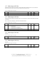
Input Bias resistor reference designators have changed as follows.
Table 1-1 Bias resistor was / is list.
Was
Is
Description
Value
Was
Is
Description
Value
R25
R1
Output Bias
470
R10
R2
Input Bias
2.2K (Typical)
R24
R4
Output Bias
470
R9
R5
Input Bias
2.2K (Typical)
R16
R9
Input Bias
2.2K (Typical)
R4
R6
Input Bias
2.2K (Typical)
R15
R8
Input Bias
2.2K (Typical)
R3
R7
Input Bias
2.2K (Typical)
Table 1-2 Other Resistor Was / Is Changes
Was
Is
Description
Value
R27
R10
Connector Shell
Optional
R23
R3
Output Bias, For Testing
100K Optional
User Manual for the PCI-OPTO32B Card, Revision: A, Manual Revision: E
General Standards Corporation
8302A Whitesburg Drive Huntsville, AL 35802, Phone: (256) 880-8787
9
1.2
Card Features
• 24 optically isolated inputs
•
Selectable input voltage range thru use of field replaceable bias resistors.
• 8 optically isolated outputs - 4 normal, 4 Diode Clamped
• Software Programmable clock debounce rate
• Software Programmable Change of State detection. Rising edge or falling edge per input channel
• Software Programmable Interrupts on any or all Change of State bit(s)
• Software Pre-loadable Event counter on Input Bit 23
• Programmable Interrupt on event counter overflow
• Built in Self-Test Features.
•
Registers are Read / Write.
•
Ability to monitor the Debounce Clock.
The board uses the PLX 9080-3 PCI interface chip to provide the advanced features of the PCI interface
environment. These features include:
• Programmable Little Endian / Big Endian swapping
• PCI cycles Asynchronous to local bus cycles
• Software Programmable board base address
User Manual for the PCI-OPTO32B Card, Revision: A, Manual Revision: E
General Standards Corporation
8302A Whitesburg Drive Huntsville, AL 35802, Phone: (256) 880-8787
10
SECTION 2
2.
INSTALLATION AND MAINTENANCE
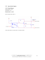
2.1
Card Configuration
Figure 1 Board Layout
User Manual for the PCI-OPTO32B Card, Revision: A, Manual Revision: E
General Standards Corporation
8302A Whitesburg Drive Huntsville, AL 35802, Phone: (256) 880-8787
11
2.2
Installation
2.2.1
Physical Installation
Selectable input voltage range thru use of field replaceable bias resistors using standard 8 pin SIP isolation resistors.
These bias resistor packages are socketed for easy replacement One bias resistor package will affect the input
channels on nibble boundaries.
2.2.2
Input / Output Cable Connectors
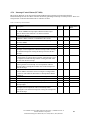
Table 2-3 Input / Output Cable Pin Assignments
PIN NUMBER
1
2
3
4
5
6
7
8
9
10
11
12
13
14
15
16
17
18
19
20
21
22
23
24
25
26
27
28
29
30
31
32
33
34
SIGNAL
IN CH00 HI
IN CH00 LO
IN CH01 HI
IN CH01 LO
IN CH02 HI
IN CH02 LO
IN CH03 HI
IN CH03 LO
IN CH04 HI
IN CH04 LO
IN CH05 HI
IN CH05 LO
IN CH06 HI
IN CH06 LO
IN CH07 HI
IN CH07 LO
IN CH08 HI
IN CH08 LO
IN CH09 HI
IN CH09 LO
IN CH10 HI
IN CH10 LO
IN CH11 HI
IN CH11 LO
IN CH12 HI
IN CH12 LO
IN CH13 HI
IN CH13 LO
IN CH14 HI
IN CH14 LO
IN CH15 HI
IN CH15 LO
IN CH16 HI
IN CH16 LO
PIN NUMBER
35
36
37
38
39
40
41
42
43
44
45
46
47
48
49
50
51
52
53
54
55
56
57
58
59
60
61
62
63
64
65
66
67
68
SIGNAL
IN CH17 HI
IN CH17 LO
IN CH18 HI
IN CH18 LO
IN CH19 HI
IN CH19 LO
IN CH20 HI
IN CH20 LO
IN CH21 HI
IN CH21 LO
IN CH22 HI
IN CH22 LO
IN CH23 HI
IN CH23 LO
LOG OUT CH0 HI
LOG OUT CH0 LO
LOG OUT CH1 HI
LOG OUT CH1 LO
LOG OUT CH2 HI
LOG OUT CH2 LO
LOG OUT CH3 HI
LOG OUT CH3 LO
PWR OUT CH4 HI
PWR OUT CH4 LO
PWR OUT CLAMP 4
PWR OUT CH5 HI
PWR OUT CH5 LO
PWR OUT CLAMP 5
PWR OUT CLAMP 6
PWR OUT CH6 HI
PWR OUT CH6 LO
PWR OUT CLAMP 7
PWR OUT CH7 HI
PWR OUT CH7 LO
User Manual for the PCI-OPTO32B Card, Revision: A, Manual Revision: E
General Standards Corporation
8302A Whitesburg Drive Huntsville, AL 35802, Phone: (256) 880-8787
12
2.3
System Configuration
2.3.1
Opto-isolated Inputs
Selectable input voltage range thru use of field replaceable bias resistors, labeled RIN, using standard 8 pin SIP
isolation resistors. These bias resistor packages are socketed for easy replacement One bias resistor package will
affect the input channels on nibble boundaries as follows:
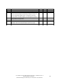
Table 2-4 Input Channels Bias Resistors Locations.
Resistor Location
R7
R6
R5
R2
R8
R9
Input Channels
IN CH00 thru IN CH03
IN CH04 thru IN CH07
IN CH08 thru IN CH11
IN CH12 thru IN CH15
IN CH16 thru IN CH19
IN CH20 thru IN CH23
Current Limiting Resistor Values should be chosen to provide a Minimum input current of 2.3 mA. Typical resistor
values for input voltage levels are as follows:
Table 2-5 Input Channels Bias Resistor Values
Input Voltage Range
5V
12 V
28 V
48 V
Bias Resistor Values
2200 ohms
5100 ohms
12000 ohms
20000 ohms
User Manual for the PCI-OPTO32B Card, Revision: A, Manual Revision: E
General Standards Corporation
8302A Whitesburg Drive Huntsville, AL 35802, Phone: (256) 880-8787
13
2.3.1.1 Channels 0-22
Isolation Voltage – 5000 V
Current Transfer Ratio – 80-600%
Min Input Current – 2.3 mA.
Max Input Current – 80 mA.
Typical Ton/Toff – 3/5 uSec.
Figure 2 Input Channels 0-22, Typical
2.3.1.2 Channel 23
Isolation Voltage – 7500 V
Min Input Current – 2.3 mA.
Max Input Current – 60 mA.
Max Ton/Toff – 4/4 uSec.
Figure 3 Input Channel 23
User Manual for the PCI-OPTO32B Card, Revision: A, Manual Revision: E
General Standards Corporation
8302A Whitesburg Drive Huntsville, AL 35802, Phone: (256) 880-8787
14
2.3.2
Opto-isolated Outputs
2.3.2.1 Normal Outputs
Isolation Voltage – 5000 V
VCEO (Max) – 60 V
Maximum Current – 100 ma.
Typical Ton/Toff – 3/5 uSec.
Figure 4 Normal Outputs, Bits 0-3
100 K isolation Resistor is Optional and is not normally installed.
User Manual for the PCI-OPTO32B Card, Revision: A, Manual Revision: E
General Standards Corporation
8302A Whitesburg Drive Huntsville, AL 35802, Phone: (256) 880-8787
15
2.3.2.2 Diode Clamped Outputs
Isolation Voltage – 5000 V
VCEO (Max) – 60 V
Maximum Current – 100 ma.
Typical Ton/Toff – 3/5 uSec.
Figure 5 Diode Clamped Outputs, Bits 4-7
User Manual for the PCI-OPTO32B Card, Revision: A, Manual Revision: E
General Standards Corporation
8302A Whitesburg Drive Huntsville, AL 35802, Phone: (256) 880-8787
16
SECTION 3
3.
CONTROL SOFTWARE
3.1
Introduction
3.2
Board Register Descriptions
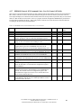
Table 3-6 Register Address Map
Board Offset
0x00
0x00
0x04
0x08
0x0c
0x010
0x014
0x018
0x01c
3.2.1
Size
8 Bits read only
8 Bits write only
24 bits Read ONLY
24 bits Read / Write
16 bits Read / Write
24 bits Read / Write
24 bits Read / Write
24 bits Read / Write
8 bits Read / Write
Register Name
Board Status Register
Board Control Register
Received data register
Change of state register
Receive Event Counter
COS Interrupt enable register
COS Polarity register
Clock Division Register
Output data register
Board Status Register - Board Offset 0x00
8 Bits read only.
Table 3-7 Board Status Register
Bit[0]
Bit[1]
Bit[2]
Bit[3]
Bit[4]
Bit[5]
Bit[6]
Bit[7]
=
=
=
=
=
=
=
=
Int_Byte_LO_Out_H ; bits 7 - 0 COS interrupt status
Int_Byte_MD_Out_H ; bits 15 - 8 COS interrupt status
Int_Byte_HI_Out_H ; Bits 23 - 16 COS interrupt status
Rx_Event_Overflow_H ; event overflow status
Master_Int_Out_ ; - master Interrupt status
Slow_Debounce_Clock ;
Enable_Rx_Event_Overflow_H ; Interrupt enable for event overflow
Fail_LED_ON_L ;
User Manual for the PCI-OPTO32B Card, Revision: A, Manual Revision: E
General Standards Corporation
8302A Whitesburg Drive Huntsville, AL 35802, Phone: (256) 880-8787
17
3.2.2
Board Control Register - Board Offset 0x00 -
8 Bits write only. Table 3-8 Board Control Register
Bit[0]
Bit[1]
Bit[2]
Bit[3]
Bit[4]
Bit[5]
Bit [6]
Bit [7]
= Clear_Int_Byte_LO_Out_H ; clear bits 7 - 0 COS interrupt status
= Clear_Int_Byte_MD_Out_H ; clear bits 15 - 8 COS interrupt status
= Clear_Int_Byte_HI_Out_H ; clear Bits 23 - 16 COS interrupt status
= Clear_Rx_Event_Overflow_H ; clear event overflow status
= Master Clear ; - clear all COS or Event Overflow.
= reserved ;
= Enable_Rx_Event_Overflow_H ; Interrupt enable.
= Fail_LED_ON_L ;
NOTE: Bits 0-4 are self-clearing pulses that are written as a 1 to clear the interrupt source. The
bits will then self clear so that another host operation is not required.
NOTE: The Clear Interrupt Bytes, or the Master Clear (bit[4]), will clear ANY COS register bit
that is set regardless of the bits Interrupt Enable Status. For Individual COS bit clearing, Write a
1 to the COS bit you wish to clear.
Event Overflow status will only be cleared by Clear Event Overflow or by Master Clear, Bit[4]. Loading the
Event Counter WILL NOT clear out the event overflow status.
3.2.3
Received data register - Board Offset 0x04
24 bits. Debounced receive data bits 0 - 23. Read ONLY.
3.2.4
Change of state register - Board Offset 0x08
24 bits - Change of state detection. Polarity programmed thru COS Polarity register, 0x014.
Read COS data bits 0 - 23. Read ONLY.
If a COS bit is set, then it will stay set until cleared by the host. A COS bit is cleared by writing a 1 to a COS bit that
is set. Writing a zero will have no effect. COS bits may also be cleared by using the board control register Byte
clears or using the board control master clear.
3.2.5
Receive Event Counter - Board Offset 0x0c
16 bits Read / Write. Written by the host.
This counter may be read at any time by the host. Counter will increment once for every Debounced Rising edge
detected on input data bit 23. When the counter is 0x0ffff and increments the Rx event overflow status bit will be set
and can be used to generate an interrupt.
3.2.6
COS Interrupt enable register - Board Offset 0x010
24 bits. Read / Write.
Each bit will be bitwise ANDED with the COS register and all of the results OR’ed together to generate an Interrupt.
A 1 will enable the corresponding interrupt. A 0 will disable that bit from generating an interrupt.
User Manual for the PCI-OPTO32B Card, Revision: A, Manual Revision: E
General Standards Corporation
8302A Whitesburg Drive Huntsville, AL 35802, Phone: (256) 880-8787
18
3.2.7
COS Polarity register - Board Offset 0x014
24 bits. Read / Write.
When the corresponding bit is zero, the COS detection for that bit will be set by a detected High to Low transition.
When Set to a 1 the COS detection for that bit will look for Low to High transitions. Reset to all zeros.
3.2.8
Clock Division Register - Board Offset 0x018
24 bits. Read / Write.
NOTE >>>> when altering this register, disable all interrupts and expect unusual results in the
COS Detection register.
A 24 Bit clock divider is provided for programmable Debounce delays. The debounce circuit registers the incoming
data 3 times in a daisy chain. When ALL 3 registers are high, the incoming data is a high. When the debounced data
register contains a 1, then ALL three registers must contain zero for the debounced data to transition back to a zero.
The clock for these holding registers is programmable thru the clock divider.
The Basic clock of the board is 20 MHz, 50 Ns. The Basic Clock Counter will always divide by 4, 200 Ns. Values of
0x0000 or 0x0001 will not alter this. When the clock divider is loaded with a larger value then the clock division will
be (count * 2) + 2. The Total debounce time will be 3 X (clock division time).
For Example: for a 15ms. debounce time. Clock period should be 5ms.
5ms / 50 Ns = 100000. -2 = 99998.
99998 / 2 = 49999 = 0x0c34f Hex.
3.2.9
Output data register - Board Offset 0x01c.
8 bits - Read / Write.
The 8 bit output data register. Reset to All Zero’s. Writing a 1 to a bit will make that opto output conductive and give
a ‘0’ to the other end. Writing a 0 will turn the opto off and allow the output to float to ‘1’.
User Manual for the PCI-OPTO32B Card, Revision: A, Manual Revision: E
General Standards Corporation
8302A Whitesburg Drive Huntsville, AL 35802, Phone: (256) 880-8787
19
4.
PLX 9080-3 Programming
4.1
Initialization.
When the PLX9080-3 is reset, it will initialize itself from an on board serial EEPROM that is programmed at
General Standards. The registers loaded at initialization are:
Table 4-9 EEPROM Register Initialization
PCI Configuration
Reg.
0x0
0x8
0x3C
PCI Register Offset
0x40
0x44
0x00
0x04
0x08
0x0c
0x10
0x14
0x18
0x1c
0x20
0x24
0x28
0x2c
Bits
Description
Value After Reset
32
32
32
Bits
32
32
32
32
32
32
32
32
32
32
32
32
32
32
Device ID / Vendor ID
Class Code / Revision ID
Max / Min Latency / Int. Pin / Int. Line Routing Value
Description
Mailbox 0 User defined
Mailbox 1 User defined
range PCI to Local
Local Base Address (remap)
Local Arbitration register
Big / little Endian descriptor
range for PCI to local expansion ROM
Local Base Address Remap PCI to Local Expansion ROM
Bus region descriptors for PCI to Local
Range for direct Master to PCI
Local base address direct Master to PCI
Local base address direct Master to PCI IO/CFG
PCI base address Remap for direct Master to PCI
PCI Configuration Address register for direct Master to PCI
IO/CFG
0x906E10B5
0x07800002
0x00000100
Value After Reset
0x00030003
0x0003000x
0xFFFFFFC1
0x0001
0x0000, Not Used
0x0000
0x0000, Not Used
0x0000, Not Used
0x40000300
0x0000, Not Used
0x0000, Not Used
0x0000, Not Used
0x0000, Not Used
0x0000, Not Used
A brief description of the PLX9080-3 Registers initialized is as follows.
4.1.1
Device ID / Vendor ID
Device ID and Vendor ID are used to identify the PCI-OPTO32B during configuration cycles.
Table 4-10 PCI Configuration ID Register Description
Field
Description
Read
Write
15:0
Vendor ID - Identifies the manufacturer of the device. Defaults to
the PCI SIG issued vendor ID of PLX if no EEPROM is present
and pin NB# (no local bus initialization) is asserted low.
Yes
Local
only
31:16
Device ID - Identifies the particular device. Defaults to the PLX
part number for PCI interface chip if no EEPROM is present and
pin NB# (no local bus initialization) is asserted low.
Yes
Local
only
User Manual for the PCI-OPTO32B Card, Revision: A, Manual Revision: E
General Standards Corporation
8302A Whitesburg Drive Huntsville, AL 35802, Phone: (256) 880-8787
Value After
Reset
10B5h
906Eh
20
4.1.2
Class Code / Revision ID
PCI Specification defined encoding to identify the type of device this is. Used primarily for Plug and Play
applications.
Table 4-11 PCI Revision ID Register Description
Field
Description
Read
Write
7:0
Revision ID. The silicon revision of the PLX9060ES.
Yes
15:8
Yes
23:16
Specific register level programming interface (00h). No interface
defined
Sub-class Encoding (80h). Other bridge device.
31:24
Base Class Encoding other Bridge Device
Yes
Local
Only
Local
Only
Local
Only
Local
Only
4.1.3
Yes
Value After
Reset
02h
00h
80h
07h
Max Latency / Min Grant / Int. Pin / Int. Line Routing Value
Latency and Grant are for DMA Applications. The PCI OPTO32 does not use DMA and these are not used. Interrupt
Pin identifies which interrupt on the PCI / PCI connector this device is connected to. The PCI-OPTO32B is
connected to INTA#. The other interrupt pins are not connected. Interrupt line routing is host dependent and should
be filled in by the host processor during PCI configuration.
Table 4-12 PCI Interrupt Line Register Description
Field
Description
Read
Write
7:0
Interrupt Line RoutingValue indicates which input of the system
interrupt controller(s) the devices interrupt line is connected to.
Interrupt Pin register. Indicates which interrupt pin the device uses.
The following values are decoded:
0 = No Interrupt Pin
1 = INTA#
2 = INTB#
3 = INTC#
4 = INTD#
Min_Gnt. Used to specify how long a burst period the device needs
assuming a clock rate of 33 MHz. Value is multiple of 1/4 usec
increments
Max_Lat. Used to specify how often the device needs to gain
access to the PCI bus. Value is multiple of 1/4 usec increments.
Yes
Yes
Yes
Local
Only
1
Yes
Local
Only
0
Yes
Local
Only
0
15:8
23:16
31:24
User Manual for the PCI-OPTO32B Card, Revision: A, Manual Revision: E
General Standards Corporation
8302A Whitesburg Drive Huntsville, AL 35802, Phone: (256) 880-8787
Value After
Reset
0
21
4.1.4
Mailbox 0 User defined
When loaded from the EE Prom, this mailbox is used to contain values to identify the PLD revision, and EE Prom
Revision levels of this board.
Table 4-13 Mailbox 0
Field
Description
Read
Write
15:0
31:16
PLD Revision Level
EE Prom Revision Level
Yes
Yes
Yes
Yes
4.1.5
Value After
Reset
0x0003
0x0003
Mailbox 1 User defined
When loaded from the EE Prom, this mailbox register is used to identify the overall PCI-OPTO32B board assembly
revision level.
Bits 0-7 will be used to identify the 3 different PCI-OPTO32B Variations.
Table 4-14 Mailbox 1
Field
Description
Read
Write
7:0
Device ID
0x00 - PCI-OPTO32B
0x01 - PCI-OPTO32B-12V-CONTACT
0x02 - PCI-OPTO32B-12V-CONTACT-8x28v
Reserved
Board Assembly Revision Level
Yes
Yes
Value After
Reset
0x0000
Yes
Yes
Yes
Yes
0x0000
0x0003
15:8
31:16
User Manual for the PCI-OPTO32B Card, Revision: A, Manual Revision: E
General Standards Corporation
8302A Whitesburg Drive Huntsville, AL 35802, Phone: (256) 880-8787
22
4.1.6
Range PCI to Local
The PCI-OPTO32B registers map into PCI I/O Space using 64 bytes of I/O Space. PCI-OPTO32B registers should
not be prefetched because they act as I/O ports.
Table 4-15 Range PCI to Local Register Description
Field
Description
Read
Write
0
Memory space indicator. A value of 0 indicates register maps into
Memory space. A value of 1 indicates the register maps into I/O
space.
Location of register:
00 - Locate anywhere in 32 bit memory address space
01 - Locate below 1 MByte memory address space
10 - Locate anywhere in 64 bit memory address space
11 –Reserved
Prefetchable. A value of 1 indicates there are no side effects on
reads.
Memory Base Address. Memory base address for access to local
address space
Yes
No
Value After
Reset
1
Yes
No
0
Yes
No
0
Yes
Yes
0xFFFFFFC
2:1
3
31:4
4.1.7
Local Base Address (remap)
Not used. This register should always be set to 0x001 to enable address decode.
Table 4-16 Local Base Address (remap)
Field
Description
Read
Write
0
Space 0 Enable. A 1 value enables Decode of PCI addresses for
Direct Slave access to local space 0. A value of 0 disables Decode.
Not Used
Yes
Yes
Value After
Reset
1
Yes
Yes
0x0000
31:1
User Manual for the PCI-OPTO32B Card, Revision: A, Manual Revision: E
General Standards Corporation
8302A Whitesburg Drive Huntsville, AL 35802, Phone: (256) 880-8787
23
4.1.8
Big / Little Endian descriptor
Upon reset, the board is configured for Little Endian operation. Bit 2 can be used to program the board for Big
Endian operation. If Endian mode is changed, Bit 4 should always be 0. Bits 0 and 1 apply to Direct Bus Master
devices, and do not apply to the PCI-OPTO32. The PCI-OPTO32B is not a direct bus master.
Table 4-17 Big/Little Endian Register Description
Field
Description
Read
Write
0
1
2
Configuration Register Big Endian mode. Does Not Apply.
Direct Master Big Endian mode. Does Not Apply.
Direct Slave Address Space 0 Big Endian mode. A 1 value
specifies that Big Endian data ordering is used for Direct Slave
accesses to local Address Space 0. A value of 0 specifies Little
Endian ordering.
Direct Slave Address Expansion ROM Big Endian select. Not
Used.
Big Endian byte lane mode. Must be 0.
Not used.
Yes
Yes
Yes
Yes
Yes
Yes
Value After
Reset
0
0
0
Yes
Yes
0
Yes
Yes
Yes
No
0
0x0000
3
4
31:5
User Manual for the PCI-OPTO32B Card, Revision: A, Manual Revision: E
General Standards Corporation
8302A Whitesburg Drive Huntsville, AL 35802, Phone: (256) 880-8787
24
4.1.9
Bus region descriptors for PCI to Local
The following values should never be altered.
Bits 1:0
0x00
Local bus is 8 bits.
Bit 6
0
Ready Input is not used.
Bit 7
0
Bterm Input is not used.
Table 4-18 Bus region descriptors for PCI to Local
Field
Description
Read
Write
1:0
Memory Space 0 Local Bus Width. Programmable for the Cx and
Jx modes only. A value 00 indicates a bus width of 8 bits. A value
of 01 indicates a bus width of 16 bit, a value of 10 or 11 indicates a
bus width of 32 bits.
Memory Space 0 Internal Wait States (data to data).
Memory Space 0 Ready Input Enable. A value of 0 disables the
Ready input.
Memory Space 0 Bterm Input Enable. A value of 0 disables the
Bterm input.
Memory Space 0 Prefetch Disable. If mapped into memory space,
a 0 enables read pre-fetching, a value of 1 disables pre-fetching. If
pre-fetching is disabled, the PLX9080-3 will disconnect after each
memory read.
Expansion ROM Space Prefetch Disable. A 0 enables read prefetching, a value of 1 disables pre-fetching. If pre-fetching is
disabled, the PLX9080-3 will disconnect after each memory read.
Read Prefetch Count Enable. When set to a 1 and memory prefetching is enabled, the PLX9080-3 will pre-fetch up to the number
of Lwords specified in the Prefetch count.
Read Prefetch Count. When the Read Pre-fetch Count Enable is set
to a 1 and memory pre-fetching is enabled, the PLX9080-3 will
pre-fetch up to the number of Lwords specified in the pre-fetch
count for memory access to the Memory Space 0 or to the
Expansion ROM.
Single Read Access Mode Enable. Used in conjunction with
Memory Space 0 and Expansion ROM Pre-fetch Disable. If a PCI
read access is made to address space 0 and space 0 Pre-fetch
Disable is set to a 1 or a PCI read access is made to Expansion
ROM space and Expansion ROM pre-fetch Disable is set to a 1,
the PLX9080-3 will perform a single read access independent of
the PCI bus byte enables. The single access is made as follows:
32 bit local bus ----- bytes 0,1,2,3
16 bit local bus ----- bytes 0,1
8 bit local bus ----- byte 0
For a 16 bit local bus, bytes 2,3 of the PCI Lword will contain
invalid data.
For an 8 bit local bus, bytes 1,2,3 of the PCI Lword will contain
invalid data.
Yes
Yes
Value After
Reset
0x00
8 bit local bus
width.
Yes
Yes
Yes
Yes
0
0
Yes
Yes
0
Yes
Yes
1
Yes
Yes
1
Yes
Yes
0
Yes
Yes
0
Yes
Yes
0
5:2
6
7
8
9
10
14:11
15
User Manual for the PCI-OPTO32B Card, Revision: A, Manual Revision: E
General Standards Corporation
8302A Whitesburg Drive Huntsville, AL 35802, Phone: (256) 880-8787
25
17:16
21:18
22
23
24
25
26
27
31:28
Expansion ROM Space Local Bus Width. Programmable for the
Cx and Jx modes only.
A value of 00 indicates a bus width of 8 bits,
a value of 01 indicates a bus width of 16 bits,
A value of 10 or 11 indicates a bus width of 32 bits.
Expansion ROM Space Internal Wait States (data to data)
Expansion ROM Space Ready Input Enable. A 1 value enables
Ready input. A value of 0 disables the Read input.
Expansion ROM Space Bterm Input Enable. A 1 value enables
Bterm input. A value of 0 disables the Bterm input.
Memory Space 0 Burst Enable. A 1 value enables bursting. A value
of 0 disables bursting
Reserved.
Expansion ROM Space Burst Enable. A 1 value enables bursting.
A value of 0 disables bursting
Direct Slave PCI write mode. A 0 indicates that the PLX9080-3
should disconnect when the Direct Slave write FIFO is full. A 1
indicates that the PLX9080-3 should de-assert TRDY when the
write FIFO is full.
PCI Target Retry Delay Clocks. Contains the value (multiplied by
8) of the # of PCI bus clocks after receiving a PCI-Local read or
write access and not successfully completing a transfer. Only
pertains to Direct Slave write when bit 27 is set to 1.
Yes
Yes
0
Yes
Yes
Yes
Yes
0
0
Yes
Yes
0
Yes
Yes
0
Yes
Yes
Yes
Yes
0
0
Yes
Yes
0
Yes
Yes
4
User Manual for the PCI-OPTO32B Card, Revision: A, Manual Revision: E
General Standards Corporation
8302A Whitesburg Drive Huntsville, AL 35802, Phone: (256) 880-8787
26
4.2
PCI Configuration Registers
After power up, the PLX interface needs to be initialized for PCI bus operation. The PCI interface is initialized thru
PCI configuration cycles.
The primary purposes of PCI configuration cycles are to:
1. Identify any boards found thru the Device ID and Vendor ID.
2. Assign addresses for memory mapped and I/O access. The base address registers at offsets 0x010 and 0x014
assign addresses for access to PLX registers. The register at offset 0x018 assigns the address for access to the
PCI-OPTO32B board registers described in section 3.2.
3. Identify Interrupt routing.
4. Enable the board for PCI bus accesses. In the PCI Status / Command register at offset 0x04 bits 0 and 1 must be
set to enable the PLX9080-3 to respond to PCI bus cycles.
All registers may be written to or read from in byte, word or long word accesses.
Table 4-19 PCI CONFIGURATION REGISTERS
PCI
CFG
Register
Address
0x00
0x04
0x08
0x0C
0x10
0x14
0x18
0x1C
0x20
0x24
0x28
0x2C
0x30
0x34
0x38
0x3C
To ensure software compatibility with other versions of PLX9080-3
family and to ensure compatibility with future enhancement. All
unused bits should be written to 0.
31
23
15
7
0
Device ID
Vendor ID
Status
Command
Class Code
Revision ID
BIST
Header Type
Latency Timer
Cache Line Size
PCI Base Address for Memory Mapped Runtime Registers
PCI Base Address for I/O Mapped Runtime Registers
PCI Base Address for Local Address Space 0
Reserved
Reserved
Reserved
Reserved
Reserved
PCI Base Address to local Expansion ROM, Not Used
Reserved
Reserved
Max lat
Min Gnt
Interrupt Pin
Interrupt Line
User Manual for the PCI-OPTO32B Card, Revision: A, Manual Revision: E
General Standards Corporation
8302A Whitesburg Drive Huntsville, AL 35802, Phone: (256) 880-8787
Value After Reset
0x906E10B5
0x02800000
0x07800002
0x00000000
0x00000000
0x00000001
0x00000001
0x00000000
0x00000000
0x00000000
0x00000000
0x00000000
0x00000000
0x00000000
0x00000000
0x00000100
27
4.2.1
PCI Configuration ID Register (Offset 00h)
Read to identify the board during configuration cycles.
Table 4-20 PCI Configuration ID Register Description
Field
Description
Read
Write
15:0
Vendor ID - Identifies the manufacturer of the device. Defaults to
the PCI SIG issued vendor ID of PLX if no EEPROM is present
and pin NB# (no local bus initialization) is asserted low.
Yes
Local
only
31:16
Device ID - Identifies the particular device. Defaults to the PLX
part number for PCI interface chip if no EEPROM is present and
pin NB# (no local bus initialization) is asserted low.
Yes
Local
only
User Manual for the PCI-OPTO32B Card, Revision: A, Manual Revision: E
General Standards Corporation
8302A Whitesburg Drive Huntsville, AL 35802, Phone: (256) 880-8787
Value After
Reset
10B5h
906Eh
28
4.2.2
PCI Command Register (Offset 04h)
Must be initialized by the Host CPU. Should be the last register initialized during configuration. Bits 0 and 1 should
be set to a 1. Bit 6 can also be set as desired. 16 bit register. If written as a 32-bit register the upper 16 bits should be
0x0280. Typical value would be 0x02800003.
Table 4-21 PCI Command Register Description
Field
Description
Read
Write
0
I/O Space. A value of 1 allows the device to respond to I/O space
accesses. A value of 0 disables the device from responding to I/O
space accesses.
Memory Space. A value of 1 allows the device to respond to
memory space accesses. A value of 0 disables the device from
responding to memory space accesses.
Master Enable. A value of 1 allows the device to behave as a bus
master. A value of 0 disables the device from generating bus
master accesses.
Special Cycle. This bit is not supported.
Memory Write/invalidate Enable. Direct Master, does not apply.
VGA Palette Snoop. This bit is not supported.
Parity Error Response. A value of 0 indicates that a parity error is
ignored and operation continues. A value of 1 indicates that parity
checking is enabled.
Wait Cycle Control. Controls whether or not the device does
address/data stepping. A 0 value indicates the device never does
stepping. A value of 1 indicates that the device always does
stepping. This value is hardwired to 0.
SERR# Enable. A value of 1 enables the SERR# driver. A value of
0 disables the driver
Fast Back-to-Back Enable. Indicates what type of fast back-to-back
transfers a Master can perform on the bus. A value of 1 indicates
that fast back-to-back transfers can occur to any agent on the bus.
A value of 0 indicates that fast back-to-back transfers can only
occur to the same agent as the previous cycle.
Reserved
Yes
Yes
Value After
Reset
0
Yes
Yes
0
Yes
Yes
0
Yes
Yes
Yes
Yes
No
Yes
No
Yes
0
0
0
0
Yes
Yes
0
Yes
Yes
0
Yes
No
0
Yes
No
0
1
2
3
4
5
6
7
8
9
15:0
User Manual for the PCI-OPTO32B Card, Revision: A, Manual Revision: E
General Standards Corporation
8302A Whitesburg Drive Huntsville, AL 35802, Phone: (256) 880-8787
29
4.2.3
PCI Status Register (Offset 06h)
The PCI Status Register affects how the PLX9080-3 will interact with the host PCI bus. This register should be left
with its default value. 16 bit register.
Table 4-22 PCI Status Register Description
Field
Description
Read
Write
6:0
7
Reserved
Fast Back-to-Back Capable. When this bit is set to a 1, it indicates
the adapter can accept fast back-to-back transactions. A 0 indicates
the adapter cannot.
Master Data Parity Error Detected. This bit is set to a 1 when three
conditions are met: l) the PLX9080-3 asserted PERR# itself or
observed PERR# asserted; 2) the PLX9080-3 was the bus master
for the operation in which the error occurred; 3) the Parity Error
Response bit in the Command Register is set. Writing a 1 to this bit
clears the bit (0)
DEVSEL Timing. Indicates timing for DEVSEL# assertion. A
value of 01 is medium.
Target Abort. When this bit is set to a 1, this bit indicates the
PLX9080-3 has signaled a target abort. Written a 1 to this bit
clears the bit (0).
Received Target Abort. When set to a 1, this bit indicates the
PLX9080-3 has received a target abort signal. Written a 1 to this
bit clears the bit (0).
Received Master Abort. When set to a 1, this bit indicates the
PLX9080-3 has received a master abort signal. Writing a 1 to this
bit clears the bit (0).
Signaled System Error. When set to a 1, this bit indicates the
PLX9080-3 has reported a system error on the SERR# signal.
Writing a 1 to this bit clears the bit (0).
Detected Parity Error. When set to a 1, this bit indicates the
PLX9080-3 has detected a PCI bus parity error, even if parity error
handling is disabled (the Parity Error Response bit in the
Command Register is clear). One of three conditions can cause this
bit to be set. 1) The PLX9080-3 detected a parity error during a
PCI address phase; 2) the PLX9080-3 detected a data parity error
when it was the target of a write; 3) the PLX9080-3 detected a data
parity error when performing a master read operation. Writing a 1
to this bit clears the bit (0).
Yes
Yes
No
No
Value After
Reset
0
1h
Yes
Yes
0
Yes
No
01h
Yes
Yes
0
Yes
Yes
0
Yes
Yes
0
Yes
Yes
0
Yes
Yes
0
8
10:9
11
12
13
14
15
User Manual for the PCI-OPTO32B Card, Revision: A, Manual Revision: E
General Standards Corporation
8302A Whitesburg Drive Huntsville, AL 35802, Phone: (256) 880-8787
30
4.2.4
PCI Revision ID Register (Offset 08h)
Identifies the silicon revision of the PLX9060ES.
Table 4-23 PCI Revision ID Register Description
Field
Description
Read
Write
7:0
Revision ID. The silicon revision of the PLX9060ES.
Yes
Local
Only
4.2.5
Value After
Reset
01h
PCI Class Code Register (Offset 09 - Oh)
Used in Plug and Play PCI applications.
Table 4-24 PCI Class Code Register Description
Field
Description
Read
Write
7:0
Yes
15:8
Specific register level programming interface (00h). No interface
defined
Sub-class Encoding (80h). Other bridge device.
23:16
Base Class Encoding other Bridge Device
Yes
Local
Only
Local
Only
Local
Only
Yes
User Manual for the PCI-OPTO32B Card, Revision: A, Manual Revision: E
General Standards Corporation
8302A Whitesburg Drive Huntsville, AL 35802, Phone: (256) 880-8787
Value After
Reset
00h
80h
07h
31
4.2.6
PCI Base Address Register for Memory Access to Runtime Registers (Offset 10h)
This register is used to set the base address to access the PLX internal registers using PCI Memory access cycles.
The defined sequence for initializing Base Addresses is as follows. PCI reset software determines how much address
space is required by writing a value of all ones (1) to a PCI Base Address register and then reading the value back.
The PLX9080-3 returns 0’s in don't care address bits, effectively specifying the address space required. The PCI
software then maps the Local Address space into the PCI Address space by programming the PCI Base Address
register.
For Example: The Host CPU will write 0xFFFFFFFF to register 0x010. The host will read back register 0x010 and
get a value of 0xFFFFFF80. Address bits 7 thru 31 are decoded. Address bits 0 thru 6 are ignored. The PLX9080-3
registers will take up 256 bytes in memory space. The Host CPU will then assign an address for Memory Access to
PLX9080-3 internal registers and write the assigned address into the base address register.
Table 4-25 PCI Base Address Register Description
Field
Description
Read
Write
0
Memory space indicator. A value of 0 indicates register maps into
Memory space. A value of 1 indicates the register maps into I/O
space.
Location of register:
00 - Locate anywhere in 32 bit memory address space
01 - Locate below 1 Mbytes memory address space
10 - Locate anywhere in 64 bit memory address space
11 –Reserved
Prefetchable. A value of 1 indicates there are no side effects on
reads.
Memory Base Address. Memory base address for access to runtime
registers (Default 256 bytes)
Memory Base Address. Memory base address for access to runtime
registers
Yes
No
Value After
Reset
0
Yes
No
0
Yes
No
0
Yes
No
0
Yes
Yes
0
2:1
3
6:4
31:7
User Manual for the PCI-OPTO32B Card, Revision: A, Manual Revision: E
General Standards Corporation
8302A Whitesburg Drive Huntsville, AL 35802, Phone: (256) 880-8787
32
4.2.7
PCI Base Address Register for I/O Access to Runtime Registers(Offset 14h)
This register is used to set the base address to access the PLX internal registers using PCI I/O access cycles.
Table 4-26 PCI Base Address Register Description
Field
Description
Read
Write
0
Memory space indicator. A value of 0 indicates register maps into
Memory space. A value of 1 indicates the register maps into I/O
space.
Reserved
I/O Base Address. Base Address for I/O access to runtime
registers.(Default 256 bytes)
I/O Base Address. Base Address for I/O access to runtime
registers.( Default 256 bytes)
Yes
No
Value After
Reset
1h
Yes
Yes
No
No
0
0
Yes
Yes
0
1
6:2
31:7
4.2.8
PCI Base Address Register for Access to Local Address Space 0 (Offset 18h)
This register is used to set the base address to access the PCI-OPTO32B registers contained on the PCI-OPTO32B
board. The PCI-OPTO32B registers are described in section 3.2. The default configuration is to place PCIOPTO32B registers into PCI I/O space using 64 bytes of I/O Space.
Table 4-27 PCI Base Address Register Description
Field
Description
Read
Write
0
Memory space indicator. A value of 0 indicates register maps into
Memory space. A value of 1 indicates the register maps into I/O
space.
Location of register:
00 - Locate anywhere in 32 bit memory address space
01 - Locate below 1 MByte memory address space
10 - Locate anywhere in 64 bit memory address space
11 –Reserved
Prefetchable. A value of 1 indicates there are no side effects on
reads.
Memory Base Address. Memory base address for access to local
address space
Yes
No
Value After
Reset
1h
Yes
No
0
Yes
No
0
Yes
Yes
0xFFFFFFC
2:1
3
31:4
User Manual for the PCI-OPTO32B Card, Revision: A, Manual Revision: E
General Standards Corporation
8302A Whitesburg Drive Huntsville, AL 35802, Phone: (256) 880-8787
33
4.2.9
PCI Interrupt Line Register (Offset 3Ch)
The Interrupt Line Routing Register should be filled in during initialization of the PCI-OPTO32B board by the host
processor. The PCI-OPTO32B will generate interrupts using the INTA# connection of the PCI location it is plugged
into. The host processor should fill in the host interrupt level that INTA# is connected to.
Table 4-28 PCI Interrupt Line Register Description
Field
Description
Read
Write
7:0
Interrupt Line Routing. Value indicates which input of the system
interrupt controller(s) the devices interrupt line is connected to.
Yes
Yes
Value After
Reset
0
4.2.10 PCI Interrupt Pin Register(Offset 3Dh)
The PCI-OPTO32B board will generate all interrupts on the INTA# line of the PCI Connector. The host should fill
in which host interrupt the INTA# line is connected to in the Interrupt Line Routing Register.
Table 4-29 PCI Interrupt Pin Register Description
Field
Description
Read
Write
7:0
Interrupt Pin register. Indicates which interrupt pin the device uses.
The following values are decoded:
0 = No Interrupt Pin
1 = INTA#
2 = INTB#
3 = INTC#
4 = INTD#
Yes
Local
Only
User Manual for the PCI-OPTO32B Card, Revision: A, Manual Revision: E
General Standards Corporation
8302A Whitesburg Drive Huntsville, AL 35802, Phone: (256) 880-8787
Value After
Reset
1
34
4.3
Shared Run Time Registers
After the board has been configured for PCI Bus operation the run time registers within the PLX9080-3 are available
to the host processor. The most important of these are the Big / Little Endian Descriptor register and the Interrupt
Control / Status register. Other registers listed provide information and can be used for special functions.
Table 4-30 SHARED RUN TIME REGISTERS
PCI
(offset from
Runtime Base
Addr)
0x0c
0x40
0x44
0x48
0x4C
0x50
0x54
0x58
0x5C
0x60
0x64
0x68
0x6C
0x70
To ensure software compatibility with other versions of PLX9080-3
family and to ensure compatibility with future enhancement. All
unused bits should be written to 0.
Big/Little Endian Descriptor Register
Mailbox Register 0
Mailbox Register 1
Mailbox Register 2
Mailbox Register 3
Reserved
Reserved
Reserved
Reserved
PCI to Local Doorbell Register
Local to PCI Doorbell Register
Interrupt Control / Status
EEPROM Control, PCI Command Codes, User I/O Control, Init Control
Device ID
Vendor ID
User Manual for the PCI-OPTO32B Card, Revision: A, Manual Revision: E
General Standards Corporation
8302A Whitesburg Drive Huntsville, AL 35802, Phone: (256) 880-8787
Value After Reset
0x0000
0x00030003
0x0003000x
0x0000
0x0000
0x0000
0x0000
0x0000
0x0000
0x0000
0x0000
0x00010100
0x00017600
0x906E10B5
35
4.3.1
Big/Little Endian Descriptor Register (PCI 0Ch)
The PCI bus is a Little Endian bus. Data is longword aligned to the lowermost byte lane. Byte 0(address 0) appears
in AD[07:00], byte 1 appears in AD[15:8], byte 2 appears in AD[23:16], byte 3 appears in AD[31:24]. The
PLX9080-3 defaults to Little Endian operation for access to the PLX device and for access to the Local PCIOPTO32B registers. The Local PCI-OPTO32B registers are designed for Little Endian operation.
The PLX9080-3 can be programmed to operate in Big Endian mode thru the use of this register. Bit 0 controls Big
Endian access to the PLX9080-3 internal registers. Bit 2 controls Big Endian access to the Local PCI-OPTO32B
registers. In Big Endian Transfers the data is longword aligned to the uppermost byte lane. Byte 0(address 0) appears
in AD[31:24], byte 1 appears in AD[23:16], byte 2 appears in AD[15:8], byte 3 appears in AD[07:00]. Bit 4 MUST
ALWAYS be 0. Bits 1 and 3 are not used.
Table 4-31 Big/Little Endian Register Description
Field
Description
Read
Write
0
1
2
Configuration Register Big Endian mode.
Direct Master Big Endian mode. Not Used.
Direct Slave Address Space 0 Big Endian mode. A 1 value
specifies that Big Endian data ordering is used for Direct Slave
accesses to local Address Space 0. A value of 0 specifies Little
Endian ordering.
Direct Slave Address Expansion ROM Big Endian select. Not
Used.
Big Endian byte lane mode. Must be 0.
Not used.
Yes
Yes
Yes
Yes
Yes
Yes
Value After
Reset
0h
0
0
Yes
Yes
0
Yes
Yes
Yes
No
0
0x0000
3
4
31:5
User Manual for the PCI-OPTO32B Card, Revision: A, Manual Revision: E
General Standards Corporation
8302A Whitesburg Drive Huntsville, AL 35802, Phone: (256) 880-8787
36
4.3.2
Mailbox Register 0 (PCI 40h)
When loaded from the EE Prom, this mailbox is used to contain values to identify the PLD revision, and EE Prom
Revision levels of this board. This is provided as information for the host processor.
Table 4-32 Mailbox Register 0 Description
Field
Description
Read
Write
15:0
31:16
PLD Revision Level
EE Prom Revision Level
Yes
Yes
Yes
Yes
4.3.3
Value After
Reset
0x0003
0x0003
Mailbox Register 1 (PCI 44h)
When loaded from the EE Prom, this mailbox register is used to identify the overall PCI-OPTO32B board assembly
revision level.
Bits 0-7 will be used to identify the 3 different PCI-OPTO32B Variations.
Table 4-33 Mailbox Register 1 Description
Field
Description
Read
Write
7:0
Device ID
0x00 - PCI-OPTO32B
0x01 - PCI-OPTO32B-12V-CONTACT
0x02 - PCI-OPTO32B-12V-CONTACT-8x28v
Reserved
Board Assembly Revision Level
Yes
Yes
Value After
Reset
0x0000
Yes
Yes
Yes
Yes
0x0000
0x0003
Value After
Reset
0
15:8
31:16
4.3.4
Mailbox Register 2 (PCI 48h)
Not Used.
Table 4-34 Mailbox Register 2 Description
Field
Description
Read
Write
31:0
32 bit mailbox register
Yes
Yes
4.3.5
Mailbox Register 3 (PCI 4Ch)
Not Used.
Table 4-35 Mailbox Register 3 Description
Field
Description
Read
Write
31:0
32 bit mailbox register
Yes
Yes
User Manual for the PCI-OPTO32B Card, Revision: A, Manual Revision: E
General Standards Corporation
8302A Whitesburg Drive Huntsville, AL 35802, Phone: (256) 880-8787
Value After
Reset
0
37
4.3.6
Interrupt Control/Status (PCI 68h)
Bits 8 and 11 MUST be set for the Local PCI-OPTO32B interrupt to generate a PCI interrupt to the host.
Doorbell interrupts are not used. Bit 16 concerns the PCI bus generating an interrupt of a local processor. There is no
local processor on the PCI-OPTO32B so Bit 16 will have no affect.
Table 4-36 Interrupt Control/Status
Field
Description
Read
Write
0
Enable Local bus LSERR#. A value of 1 will enable the PLX90803 to assert LSERR# interrupt output when the PCI bus Target
Abort or Master Abort status bit is set in the PCI Status
Configuration Register.
Enable Local bus LSERR# when a PCI parity error occurs during a
PLX9080-3 Master Transfer or a PLX9080-3 Slave access.
Generate PCI bus SERR#. When this bit is 0, writing a 1 generates
a PCI bus SERR#.
Not Used
PCI interrupt enable. A value of 1 will enable PCI interrupts
PCI doorbell interrupt enable. A value of 1 will enable doorbell
interrupts. Used in conjunction with PCI interrupt enable. Clearing
the doorbell interrupt bits causing the interrupt will clear the PCI
interrupt.
PCI Abort interrupt enable. A value of 1 will enable a master abort
or master detect of a target abort to generate a PCI interrupt . Used
in conjunction with PCI interrupt enable. Clearing the abort status
bits will clear the PCI interrupt.
PCI local interrupt enable. A value of 1 will enable a local interrupt
input to generate a PCI interrupt. Use in conjunction with PCI
interrupt enable. Clearing the local bus cause of the interrupt will
clear the interrupt.
Retry Abort Enable. A value of 1 will enable the PLX9080-3 to
treat 256 Master consecutive retries to a Target as a Target Abort.
A value of 0 will enable the PLX9080-3 to attempt Master Retries
indefinitely.
A value of 1 indicates that the PCI doorbell interrupt is active.
A value of 1 indicates that the PCI abort interrupt is active.
A value of 1 indicates that the local interrupt input is active.
Local interrupt output enable. A value of 1 will enable Local
interrupt output.
Local doorbell interrupts enable. A value of 1 will enable doorbell
interrupts Used in conjunction with Local interrupt enable.
Clearing the Local doorbell interrupt bits causing the interrupt will
clear the interrupt
Yes
Yes
Value After
Reset
0
Yes
Yes
0
Yes
Yes
0
Yes
Yes
Yes
No
Yes
Yes
0
1
0
Yes
Yes
0
Yes
Yes
0
Yes
Yes
0
Yes
Yes
Yes
Yes
No
No
No
Yes
0
0
0
1
Yes
Yes
0
1
2
7:3
8
9
10
11
12
13
14
15
16
17
User Manual for the PCI-OPTO32B Card, Revision: A, Manual Revision: E
General Standards Corporation
8302A Whitesburg Drive Huntsville, AL 35802, Phone: (256) 880-8787
38
19:18
20
22:21
23
24
26:25
27
31:28
Not Used
A value of 1 indicates that the Local doorbell interrupt is active
Not Used
A value of 1 indicates that the BIST interrupt is active. The BIST
(built in self-test) interrupt is generated by writing a 1 to bit 6 of
the PCI Configuration BIST register. Clearing bit 6 clears the
interrupt. Refer to the BIST register for a description of self-test.
A value of 0 indicates that a Direct Master was the bus master
during a Master or Target abort.
Not Used
A value of 0 indicates that a Target Abort was generated by the
PLX9080-3 after 256 consecutive Master retries to a Target.
Not Used
Yes
Yes
Yes
Yes
No
No
No
No
0
0
0
0
Yes
No
0
Yes
Yes
No
Yes
0
0
Yes
No
0
User Manual for the PCI-OPTO32B Card, Revision: A, Manual Revision: E
General Standards Corporation
8302A Whitesburg Drive Huntsville, AL 35802, Phone: (256) 880-8787
39
4.3.7
EEPROM Control, PCI Command Codes, User I/O Control (PCI 6Ch)
This register is not used in normal operation. It does contain special bits that could be used in special circumstances.
Bits 15 thru 8 will have no affect, the PCI-OPTO32B does not generate direct bus master cycles. Bits 16 and 17,
User Output and Input, are connected on the board but at this time do not perform any function, they are reserved for
future use. Bits 24 thru 28 can be used to read, or re-program, the PLX configuration EEPROM, they should never
be used without consulting the factory. Bit 30 will perform a software reset of the local side of the PCI-OPTO32,
everything on the board except the PLX9060ES.
Table 4-37 EEPROM Control, PCI Command Codes, User I/O Control
Field
Description
Read
Write
7:0
11:8
15:12
16
Not Used
PCI Memory Read Command Code for Direct Master
PCI Memory Write Command Code for Direct Master
General Purpose Output. A value of 1 will cause the USERO
output to go high. A value of 0 will cause the output to go low.
General Purpose Input. A valve of 1 indicates that USERI input pin
is high. A value of 0 indicates that USERI pin is low.
Not Used
EEPROM clock for Local or PCI bus reads or writes to EEPROM.
Toggling this bit generates an EEPROM clock. Refer to the
manufacturer's data sheet for the particular EEPROM being used.
EEPROM chip select. For Local or PCI bus reads or writes to
EEPROM, setting this bit to a 1 provides the EEPROM chip select.
Write bit to EEPROM. For writes, this output bit is the input to the
EEPROM. The EEPROM clock clocks it into the EEPROM.
Read EEPROM data bit. For reads, this input bit is the output of
the EEPROM. The EEPROM clock clocks it out of the EEPROM.
EEPROM present. A 1 in this bit indicates that an EEPROM is
present.
Reload Configuration Registers. When this bit is 0, writing a 1
causes the PLX9080-3 to reload the PCI configuration registers
from EEPROM.
PCI Adapter Software Reset. A value of 1 written to this bit will
hold the local bus logic in the PLX9080-3 reset and LRESETO#
asserted. The contents of the PCI configuration registers and
Shared Run Time registers will not be reset. Software Reset can
only be cleared from the PCI bus.
Local Init Status 1 = local init done. Responses to PCI accesses
will be RETRYs until this bit is set. While Input NB# is asserted
low this bit will be forced to 1.
Yes
Yes
Yes
Yes
No
Yes
Yes
Yes
Value After
Reset
0
0110
0111
1
Yes
No
-
Yes
Yes
No
Yes
0
0
Yes
Yes
0
Yes
Yes
0
Yes
No
-
Yes
No
0
Yes
Yes
0
Yes
Yes
0
Yes
Yes
0
17
23:18
24
25
26
27
28
29
30
31
User Manual for the PCI-OPTO32B Card, Revision: A, Manual Revision: E
General Standards Corporation
8302A Whitesburg Drive Huntsville, AL 35802, Phone: (256) 880-8787
40
4.3.8
PCI Configuration ID Register(PCI 70h)
The Device ID and Vendor ID can be read at this offset using normal PCI bus reads, configuration cycles are not
required. It is useful for device driver troubleshooting.
Table 4-38 PCI Configuration ID Register Description
Field
Description
Read
Write
15:0
Vendor ID – Identifies the manufacturer of the device. Defaults to
the PCI SIG issued vendor ID of PLX. If no EEPROM is present
and pin NB# (no local bus initialization) is asserted low.
Device ID – Identifies the particular device. Defaults to the PLX
part number for PCI interface chip if no EEPROM is present and
pin NB# (no local bus initialization) is asserted low.
Yes
No
Value After
Reset
10B5h
Yes
No
906Eh
31:16
User Manual for the PCI-OPTO32B Card, Revision: A, Manual Revision: E
General Standards Corporation
8302A Whitesburg Drive Huntsville, AL 35802, Phone: (256) 880-8787
41
Appendix A
INTERRUPTS:
For Interrupt Operation, the Desired Interrupts are Enabled on the Opto isolator board AND Interrupts MUST be
enabled At / Thru the PLX Interface chip. To enable Event Counter Overflow Interrupts, Bit[6] of the Board Control
Register must be set to a 1.
outportb(Opto_register_base_address + 0x00, 0xc0 );
// Byte write, Turn LED off, Enable Event Overflow Interrupt.
outportl(Opto_register_base_address + 0x0c, 0x0fffe );
// Long word write, Event Counter, -2.
// The Second Rising Edge detected will generate the Interrupt
To Enable COS Interrupts, Any / All Desired COS Interrupt bit’s are enabled thru the COS Interrupt Enable
Register.
outportl(Opto_register_base_address + 0x010, 0x08421 ) ;
// Long word write, Offset 0x010, Enable Interrupts on
// COS Bit’s 0, 5, 10, and 15.
All other Machine dependent actions should be taken before the final steps in the process. Make ABSOLUTELY
sure that there is NO Pending status laying around that is already setting an interrupt action. Either use the master
clear’s
outportb(Opto_register_base_address + 0x00, 0xdf );
// Byte write, Turn LED off, Enable Event Overflow Interrupt.
// Master Clear All COS and Clear the Event Counter overflow .
// NOTE NOTE NOTE NOTE
// The Master Clear will Clear ALL COS Bits.
// The Byte Clear’s will ALSO Clear ALL COS Bits in that Byte.
// To Only Clear the Bit generating the Interrupt,
// you must use the individual Clear’s as
// Described below.
Or, Individual Clears for the COS and Event Overflow.
Outportl(Opto_register_base_address + 0x08, 0x08421 ) ;
// Long word write, Offset 0x08, COS register, Clear
// COS Bit’s 0, 5, 10, and 15. If they are set.
Outportb(Opto_register_base_address + 0x00, 0xc8 );
// Byte write, Turn LED off, Enable Event Overflow Interrupt.
// Clear Event Overflow
The final step is the write to the PLX interface that will enable it to generate Interrupts onto the PCI bus.
Outportl(PLX_io_base_address + 0x068, 0x00900 );
// Long word write, PLX interrupt control register,
// Bit’s 8 and 11, Enable Local input to generate PCI interrupts
User Manual for the PCI-OPTO32B Card, Revision: A, Manual Revision: E
General Standards Corporation
8302A Whitesburg Drive Huntsville, AL 35802, Phone: (256) 880-8787
42
In the Interrupt Handler, there is NO action required to / with the PLX Interface chip. The only requirement to
remove the Asserted interrupt is to remove the Local source of the interrupt. Which would be the COS bit or the
event overflow.
temp = inportb(Opto_register_base_address + 0x00 ) ;
// Read the OPTO Board Status register
if ( (temp & 0x010) == 1 )
{
// Master Interrupt bit will be set in the Board Status
// Register if this board generated the Interrupt.
// Status Bits 0 thru 3 could also be examined to
// Determine Which Byte generated the Interrupt
// Or if the Event Counter Overflow generated
// The Interrupt.
.
.
.
.
// Finished processing, Now It’s time to clear the
// Pending Interrupt.
Outportl(Opto_register_base_address + 0x08, 0x08421 ) ;
// Long word write, Offset 0x08, COS register, Clear
// COS Bit’s 0, 5, 10, and 15. If they are set.
Outportb(Opto_register_base_address + 0x00, 0xc8 );
// Byte write, Turn LED off, Enable Event Overflow Interrupt.
// Clear Event Overflow
}
To Disable All Interrupt’s From the OPTO board, write to the PLX interface Chip.
Outportl(PLX_io_base_address + 0x068, 0x0000 );
// Long word write, PLX interrupt control register,
// Clear Bit’s 8 and 11, disable All PCI interrupts
User Manual for the PCI-OPTO32B Card, Revision: A, Manual Revision: E
General Standards Corporation
8302A Whitesburg Drive Huntsville, AL 35802, Phone: (256) 880-8787
43