1
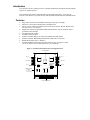
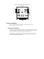
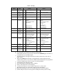
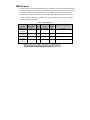
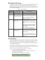
ComSync/104 PC/104 serial communications User Manual Connect Tech Inc 42 Arrow Road Guelph, Ontario N1K 1S6 Tel: 519-836-1291 Toll: 800-426-8979 Fax: 519-836-4878 Email: sales@connecttech.com URL: http://www.connecttech.com CTIM-00012, Revision 0.04, June 2007 Limited Lifetime Warranty Connect Tech Inc. provides a Lifetime Warranty for all Connect Tech Inc. products. Should this product, in Connect Tech Inc.'s opinion, fail to be in good working order during the warranty period, Connect Tech Inc. will, at its option, repair or replace this product at no charge, provided that the product has not been subjected to abuse, misuse, accident, disaster or non Connect Tech Inc. authorized modification or repair. You may obtain warranty service by delivering this product to an authorized Connect Tech Inc. business partner or to Connect Tech Inc. along with proof of purchase. Product returned to Connect Tech Inc. must be pre-authorized by Connect Tech Inc. with an RMA (Return Material Authorization) number marked on the outside of the package and sent prepaid, insured and packaged for safe shipment. Connect Tech Inc. will return this product by prepaid ground shipment service. The Connect Tech Inc. Lifetime Warranty is defined as the serviceable life of the product. This is defined as the period during which all components are available. Should the product prove to be irreparable, Connect Tech Inc. reserves the right to substitute an equivalent product if available or to retract Life Time Warranty if no replacement is available. The above warranty is the only warranty authorized by Connect Tech Inc. Under no circumstances will Connect Tech Inc. be liable in any way for any damages, including any lost profits, lost savings or other incidental or consequential damages arising out of the use of, or inability to use, such product. Copyright Notice The information contained in this document is subject to change without notice. Connect Tech Inc. shall not be liable for errors contained herein or for incidental consequential damages in connection with the furnishing, performance, or use of this material. This document contains proprietary information that is protected by copyright. All rights are reserved. No part of this document may be photocopied, reproduced, or translated to another language without the prior written consent of Connect Tech, Inc. Copyright 2007 by Connect Tech, Inc. Trademark Acknowledgment Connect Tech, Inc. acknowledges all trademarks, registered trademarks and/or copyrights referred to in this document as the property of their respective owners. Not listing all possible trademarks or copyright acknowledgments does not constitute a lack of acknowledgment to the rightful owners of the trademarks and copyrights mentioned in this document. Customer Support Overview If you experience difficulties after reading the manual and/or using the product, contact the Connect Tech reseller from which you purchased the product. In most cases the reseller can help you with product installation and difficulties. In the event that the reseller is unable to resolve your problem, our highly qualified support staff can assist you. Our support section is available 24 hours a day, seven days a week on our website at: www.connecttech.com/sub/support/support.asp. See the contact information section below for more information on how to contact us directly. Our technical support is always free. Contact Information We offer three ways for you to contact us: Telephone/Facsimile Technical Support representatives are ready to answer your call Monday through Friday, from 8:30 a.m. to 5:00 p.m. Eastern Standard Time. Our numbers for calls are: Telephone: Telephone: Facsimile: 800-426-8979 (North America only) 519-836-1291 (Live assistance available 8:30 a.m. to 5:00 p.m. EST, Monday to Friday) 519-836-4878 (on-line 24 hours) Email/Internet You may contact us through the Internet. Our email and URL addresses are: sales@connecttech.com support@connecttech.com www.connecttech.com Mail/Courier You may contact us by letter and our mailing address for correspondence is: Connect Tech Inc. Technical Support 42 Arrow Road Guelph, Ontario Canada N1K 1S6 Note: Please go to the Download Zone or the Knowledge Database in the Support Center on the Connect Tech website for product manuals, installation guides, device driver software and technical tips. Submit your technical support questions to our customer support engineers via the Support Center on the Connect Tech website. Table of Contents Limited Lifetime Warranty ................................................................................................. 2 Copyright Notice................................................................................................................. 2 Trademark Acknowledgment.............................................................................................. 2 Customer Support Overview............................................................................................... 3 Contact Information ................................................................................................................ 3 Table of Contents................................................................................................................ 4 List of Figures ..................................................................................................................... 4 List of Tables ...................................................................................................................... 4 Introduction......................................................................................................................... 5 Introduction......................................................................................................................... 5 Features ................................................................................................................................... 5 Hardware Installation.......................................................................................................... 6 Innovative I/O Structure.......................................................................................................... 6 DMA Support.......................................................................................................................... 8 85230 Register Bit Cloning..................................................................................................... 9 Security Feature ...................................................................................................................... 9 Software Selectable IRQs ..................................................................................................... 10 Shared IRQ (Revision C and proceeding)............................................................................. 10 IRQ Pull-Down (Revision C and proceeding) ...................................................................... 10 Software Selectable Line Interface Modes ........................................................................... 11 Line Termination................................................................................................................... 12 RS485 Modes (Revision C and proceeding)......................................................................... 12 I/O Connect Pin Assignments ............................................................................................... 13 I/O Address and I/O Mode Setup ................................................................................................... 14 List of Figures Figure 1: ComSync104 board layout preceeding Revision C ......................................................................... 5 Figure 2: ComSync104 Revision C/D board layout........................................................................................ 6 Figure 3: Line Termination........................................................................................................................... 12 List of Tables Table 1: I/O Map ............................................................................................................................................ 7 Table 2: DMA Support................................................................................................................................... 8 Table 3: Register Bit Cloning ......................................................................................................................... 9 Table 4: IRQs ............................................................................................................................................... 10 Table 5: Line Interface Mode Settings ......................................................................................................... 11 Table 6: Control Bits .................................................................................................................................... 12 Table 7: Pin Assignments ............................................................................................................................. 13 Table 8: I/O Address Selection..................................................................................................................... 14 Introduction The Connect Tech Inc. ComSync/104 is a 2 channel Synchronous/Asynchronous Serial Adapter card for PC/104 Bus systems. The card utilizes the features and functionality of the Zilog 85230 ESCC , along with an innovative I/O structure, to provide the user with full featured SYNC/ASYNC communications. Features ● ● ● ● ● ● ● ● ● ● Zilog 85230 clocked at 19.6608 MHz, allowing bit rates up to 4.9 Mbps Innovative I/O structure featuring basic and enhanced I/O Choice of seven software selectable electrical interfaces: RS-232, RS-422, RS-449, EIA530, EIA-530/A, V.35 and X.21 Support four software programmable DMA (Direct Memory Access) channels with TC (Terminal Count) interrupt 85230 Register Bit Cloning Available security features Software selectable IRQ on PC/104 bus, and Master Interrupt Enable Software selectable Shared IRQ and Pull-Down modes (Rev C and later) RS485 Mode support (Rev C and later) Available Industrial Temperature operating range of -40 to 85 degrees Celsius (-40 to 185 degrees F) at a reduced clock rate (14.7456 MHz) Figure 1: ComSync/104 board layout preceeding Revision C Zilog 85230 ESCC Pin 1 Pin 26 Channel B Channel A Channel B ComSync/104 65859 Rev. CTIB-00020 Pin 1 P5 Made in Canada P4 (c) 2002 Connect Tech Inc. SW1 DIP Switch SW1 Pin 26 Channel A ON IO Addr I/O address I/O mode Line termination IO Mode TE A B P1 C D P3 P2 PC/104 bus connector B A Figure 2: ComSync104 Revision C/D board layout Zilog 85230 ESCC Pin 1 Pin 26 Channel B Channel A Channel B ComSync/104 65859 Rev.C CTIB-00020 Pin 1 P5 Pin 26 Channel A P4 DIP Switch SW1 SW1 I/O address I/O mode Line termination ON IO Addr IO Mode A TE B P1 C D P3 B A P2 PC/104 bus connector Hardware Installation Be sure to configure all dip-switch settings prior to the physical installation of your ComSync/104 adapter into your PC/104 stack. Innovative I/O Structure The innovative I/O structure supports either a Basic mode or Enhanced mode of I/O interfacing. The Basic mode decodes 16 (eight prior to Revision C) consecutive I/O addresses of which 10 are used, which supports the ESCC along with Control and Status functions. The Enhanced mode is 64 consecutive I/O addresses which supports the Basic mode plus an additional I/O region which allows the ESCC registers to be read/written in one PC/104 Bus cycle. The following table shows the I/O Map. Table 1: I/O Map I/O Address (Offset) 0 1 2 3 4 5 Function Name Channel(A) Data [1] Channel(A) Control [1] Channel(B) Data [1] Channel(B) Control [1] Status and Control TC & Security 85230 Control Misc Control 6 7 8 [8] 9 [8] 0x20 » 0x2F [6] 0x30 » 0x3F [6] 0»7 Bit Definitions (Write) 85230 Data register 0»7 Bit Definitions (Read) 85230 Data register 0»7 85230 Control register 0»7 85230 Control register 0»7 85230 Data register 0»7 85230 Data register 0»7 85230 Control register 0»7 85230 Control register 0 1 2 3»5 DTR(A) [2] DTR(B) Security Feature Enable IRQ Selection 6 7 any DMA Enable (B) DMA Enable (A) Clear TC Interrupt [3] 0 1 2 3 4 5 6 7 0»7 DSR(A) DSR(B) Security Feature Enable 85230 INT pin I/O mode TC Interrupt[3] DMA Enable (B) DMA Enable (A) Security Function any Resets 85230 and Register Bit Clones [5] Line Interface Mode (A) Line Interface Mode (B) Master Interrupt Enable WAIT/TC Enable [4] Shared IRQ Enable IRQ Pull-Down Enable Reserved IRQ Selection [9] Master Interrupt Enable [10] Software IRQ [11] RX and TX RS485 Modes [7] Reserved Register Write data 0»7 85230 Interrupt Acknowledge 0»2 3»5 6 7 0 1 2 3»5 6 7 0»3 4»7 0»7 Line Interface Mode (A) Line Interface Mode (B) Master Interrupt Enable WAIT/TC Enable [4] Shared IRQ Enable IRQ Pull-Down Enable Reserved IRQ Selection Master Interrupt Enable Software IRQ RX and TX RS485 Modes [7] Reserved Register Read data Register Write data 0»7 Register Read data 0»2 3»5 6 7 IRQ 0 Control 1 2 3»5 6 7 RS485 0»3 Control 4 » 7 Channel(A) 0 » 7 Registers Channel(B) 0 » 7 Registers Notes [1] [2] [3] [4] [5] [6] [7] [8] [9] [10] [11] See Zilog ESCC user manual for description of functionality. DTR control from this I/O point is only valid when the /DTR//REQ pin of the ESCC is programmed for use as a DMA request. TC is the Terminal Count signal from the PC/104 Bus, which occurs at the end of a DMA transfer. When the /W//REQ pin of the ESCC is programmed as a WAIT function, this bit enables WAIT states to occur on the PC/104 Bus. When both channels are programmed to operate in DMA mode, this bit becomes a TC Interrupt Enable. 85230 Registers bits which are cloned. Only when Enhanced Addressing mode is enabled. Refer to description below for bit meanings. I/O Offsets [8] and [9] are only available on Revision C (or later) cards. IRQ Selection can be set at I/O Offset [8] and [4] (same bit numbers). Master Interrupt Enable can be set at I/O Offset [8] and [7] (same bit number). Software IRQ will cause the card to generate an IRQ and is mostly used for testing. DMA Support To allow fast data reception and transmission, the ComSync/104 supports four DMA channels; each one is assigned to one of the ESCC DMA Request pins. Each channel of the ESCC has 2 request pins which can be programmed as either a combined receive/transmit request or as separate receive and transmit requests (see the ESCC Users Manual for much more detail). The I/O of this card will support a DMA Enable for each Channel of the ESCC. The DMA support is organized as follows: Table 2: DMA Support PC/104 DMA signals DRQ0 / DACK0# DRQ1 / DACK1# DRQ2 / DACK2# DRQ3 / DACK3# 85230 DMA pin /DTR//REQA 85230 Chan nel A 85230 Register Bit WR14.2 = 1 Enable Bit I/O(4).7 Function Transmit DMA /W//REQA A WR1.6 = 1 I/O(4).7 Receive or Transmit DMA /DTR//REQB B WR14.2 = 1 I/O(4).6 Transmit DMA /W//REQB B WR1.6 = 1 I/O(4).6 Receive or Transmit DMA Note: If a Floppy drive is installed in the system then DRQ2/DACK2# are used and should not be used for the ComSync/104. 85230 Register Bit Cloning Various features of the ComSync/104 board are set up when certain register bits of the ESCC are programmed. This feature is extremely convenient and reduces the redundancy of setup functions. When certain bits are written to ESCC registers, the card keeps a copy of those bits to perform the setup of card features. These Register bits are cloned for each channel of the ESCC, to perform the following functions: Table 3: Register Bit Cloning ESCC Register Bit(s) Cloned WR11.2 WR4.[5,4,3,2] WR1.6 Function on ESCC Function on Card TRxC pin as an Input or Output (Reset state is an Input) Various SYNC modes which require the SYNC pin to be an Input (Reset to Async mode). Controls the direction of the TRxC(±) pins of the Line Interface to match the setting of the ESCC. Controls the direction of the SYNC(±) pins of the Line Interface to match the setting of the ESCC. Changes functionality of the /W//REQ pin (Reset state is the WAIT function). (SYNC is an input when External SYNC is selected or Async mode is selected. All other times SYNC is an Output). When programmed to the WAIT function, and the WAIT Enable [I/O(7).7] bit is ON, the card will generate wait states onto the PC/104 Bus during Data reads or writes (using the IOCHRDY signal). USE EXTREME CAUTION WHEN USING THIS MODE, INFINITE WAIT PERIODS CAN OCCUR! WR14.2 Changes the functionality of the /DTR//REQ pin (Reset state is the DTR function). When programmed for the REQ function the ESCC pin becomes the DMA signal DRQn When programmed to the DTR function, the DTR(±) signals on the line interface are supplied by the ESCC (WR5.7) and the DMA signal DRQn is disabled. When programmed to the REQ function, the ESCC pin becomes the DMA signal DRQn, and the DTR(±) line interface signals are provided by the I/O(4).0,1 bits. Security Feature Due to the specialized nature of this product, users may wish to “Secure” their software to the use of the CTI hardware. This is similar to the use of a “Software Security Dongle” (sometimes attached to a Parallel port of a PC). The function is implemented by CTI engineers (with customer input) and can be customer specific. It is programmed into the PLD logic component on the card during manufacturing. The security feature is enabled by setting I/O (4).2, setting the required security bits (this is customer specific), and then reading back the result from I/O (5). When finished with the security feature, the bit at I/O (4).2 is cleared to return to normal operation. When the security feature is enabled the following functions are inhibited: • Master Interrupt Enable cannot be changed. • WAIT states are disabled (IOCHRDY will not activate on PC/104 bus cycles). • WAIT Enable cannot be changed. • Line Interface Mode cannot be changed for either channel. Note: The function which can be programmed is limited in scope and is NOT as fully featured as one would find on a typical “Security Dongle”, but it is usually sufficiently cryptic to slow down pirates. Software Selectable IRQs There are eight IRQ numbers which can be selected by software along with a Master Interrupt Enable as follows: Table 4: IRQs Master Enable I/O (7).6 Setting I/O (4).3 » 5 IRQ Selected (Enabled) 1 1 1 1 1 1 1 1 0 1 2 3 4 5 6 7 3 5 7 9 10 11 12 15 Since the interrupt is programmable, the card powers-up with all interrupt driving circuits tristated. During software initialization of the card, both channels of the ESCC should be set up first, then the desired interrupt should be programmed and finally the Master Interrupt Enable bit set [I/O (7).6]. At this point the chosen IRQ signal will be driven inactive (low). When the SCC generates an interrupt, the selected IRQ will be driven active (high) by the card. When the interrupt has been serviced, the IRQ signal will return to the inactive state. (The IRQ signal is never tri-stated during this process). On most PC/104 buses the IRQ signals are positive edge activated with a pull-up resistor on the IRQ signal (usually located on the PC/104 CPU module). Therefore, it is possible to generate a “phantom” interrupt when the Master Interrupt Enable bit is turned off. During the shutdown of the card (when a software driver is stopped or disabled by the operating system), the interrupt should first be disconnected/disabled from the operating system and then the Master Interrupt Enable bit turned off. A false interrupt can be prevented in this way. Shared IRQ (Revision C and proceeding) The Selected IRQ can be shared between multiple ComSync/104 cards. This shared IRQ mechanism is designed using the guidelines in the PC/104 Specification V 2.5, appendix C. To enable Shared IRQ, turn On the Shared IRQ Enable bit I/O (8).0. When this bit is On, the IRQ signal will be tri-stated when it is inactive and driven high when active. A pull-down resistor is required on the IRQ signal to allow it to operate correctly (See IRQ Pull-Down). IRQ Pull-Down (Revision C and proceeding) As noted in the Shared IRQ section, the chosen IRQ requires a pull-down resistor (1K) in order to operate correctly. There can be only one pull-down resistor for each shared IRQ. To enable the pull-down, turn On the pull-down Enable bit, I/O (8).1. This activates a 1K pull-down (to GND) resistor on the programmed IRQ. Remember if you have two or more cards sharing an IRQ, only one of them should have the pull-down enabled. Software Selectable Line Interface Modes The Serial Line Interface utilizes Sipex devices SP507 (on Revision A and B cards) or SP508 (on Revision C and proceeding cards). Refer to the data sheet for these devices for all electrical characteristics of the interface. The Line Interface Mode is software selectable for each Channel. The following Modes are available: Table 5: Line Interface Mode Settings Line Interface Mode Settings (binary values) I/O address offset 7: bits 0, 1, 2 are for Channel A & bits 3, 4, 5 are for Channel B 26 Pin 25 pin Header D-Sub 000 001 010 011 100 101 110 111 [1] [1] 2 14 V.11 V.11 V.11 V.11 V.35[6] V.11 [6] [1] 3 2 V.11 V.11 V.11 V.11 V.35 V.11 V.28 [5] [5] [5] [5] [6] [5] [2] [2] 6 16 V.11 V.11 V.11 V.11 V.35 V.11 [5] [5] [5] [5] [6] [5] [2] 5 3 V.28 V.11 V.11 V.11 V.11 V.35 V.11 [1] [1] [1] [1] 20 23 V.11 V.11 V.11 V.11 [1] 14 20 V.11 V.10 V.11 V.11 V.28 V.11 V.28 [1] [1] [1] 12 19 V.11 V.11 V.11 V.11 V.11 [1] 7 4 V.11 V.11 V.11 V.11 V.28 V.11 V.28 [2] [2] [2] 25 13 V.11 V.11 V.11 V.11 V.11 [2] 9 5 V.11 V.11 V.11 V.11 V.28 V.11 V.28 [2] [2] [2] [2] 18 22 V.11 V.11 V.11 V.11 [2] 11 6 V.11 V.10 V.11 V.11 V.28 V.11 V.28 [2] [2] [2] [2] [2] [2] [2] [2] 19 10 [2] 15 8 V.10 V.10 V.10 V.10 V.28 V.10 V.28 [2] 17 9 V.11[5] V.11[5] V.11[5] V.11[5] V.35[6] V.11[5] [2] [5] [5] [5] [5] [6] [5] [2] 8 17 V.11 V.28 V.11 V.11 V.11 V.35 V.11 [1] [1] [1] V.11 V.11 V.11 V.11 V.11 21 11 [2] [2] [2] V.11 V.11 V.11 V.11 V.11 [1] V.11 V.11 V.11 V.11 V.28 V.11 V.28 22 24 [2] V.11 V.11 V.11 V.11 V.28 V.11 V.28 [6] [1] [1] V.11 V.11 V.11 V.11 V.35 V.11 23 12 [5] [5] [5] [5] [6 [5] [2] [1] V.11 V.11 V.11 V.11 V.35 ] V.11 [6] [1] V.11 V.11 V.11 V.11 V.35 V.11 V.28 4 15 [1] V.11[5] V.11[5] V.11[5] V.11[5] V.35[6] V.11[5] V.28 1, 13 1, 7 GND GND GND GND GND GND GND GND Pin# Signal TX+ TXRX+ RXDTR+ DTRRTS+ RTSCTS+ CTSDSR+ DSRDCD+ DCDRTxC+ RTxCSYNC+[3] [4] SYNC-[3] [4] TRxC+[3] [4] TRxC-[3] [4] GND Notes: [1] Tri-State [2] Hi-Z, resistance >= 10K Ω to GND [3] When Signal is an Output. [4] When Signal is an Input [5] 120 Ω termination resistor is applied between the (+) and (-) signals. [6] V.35 Termination Network is applied between the (+) and (-) signals. V.10 = RS-423 V.11 = RS-422 V.28 = RS-232 V.35 = V.35 Line Termination The multi-mode transceiver provides line termination networks built into the chip. Switches 5 and 6 on DIP switch SW1 disable or enable these networks for channels A and B on the ComSync/104. Please contact Connect Tech support for more information concerning these line termination networks. Please refer to the Line Interface Mode table listed above concerning the ComSync/104 signal assignments and related notes. Figure 3: Line Termination DIP switch – SW1 Line termination enable/disable switches ON ON = enable line termination OFF = disable line termination 1 2 3 4 5 6 This example shows the default setting with RX, RTxC and TRxC Receiver Terminations disabled: SW1-5 is set OFF for Channel A SW1-6 is set OFF for Channel B RS485 Modes (Revision C and proceeding) The ESCC can manipulate the /RTS signal to perform a variety of Line Transceiver enabling, and other signaling, related to operation in either asynchronous or SDLC modes. Refer to sections 4.2.1 and 4.4.1 of the Zilog ESCC manual. Also see the description for registers WR5.1, WR7.2 and WR10.2 for additional information about RTS control operations on the ESCC. The card allows the RTS signal to control the Line Transceivers for the TX and RX (TX± and RX±) signals only. A two-wire (Half Duplex) or four-wire (Multi-Drop) style of interface can be achieved. Note: The ESCC does not control RTS completely autonomously; software is required to perform some of the RTS control. Table 6: Control Bits I/O Offset 9 Control Bit 0 1 2 3 Function RTS State Operation RX-RTS Enable, Channel A Allow RTS to control RX Enable [1] TX-RTS Enable, Channel A Allow RTS to control TX Tri-State RX-RTS Enable, Channel B Allow RTS to control RX Enable [1] TX-RTS Enable, Channel B Allow RTS to control TX Tri-State On (RTS = low) Off (RTS = high) On (RTS = low) Off (RTS = high) Same as above RX Receiver will be disabled RX Receiver will be enabled TX Driver will be enabled TX Driver will be Tri-stated Same as above Same as above Same as above Notes [1] The RX Enable control bit function will only operate if the TX Enable bit is also On. Examples Half Duplex Setup To create this setup, both the RX-RTS Enable and TX-RTS Enable bits should be turned on, for the desired channel. For example: Bits 0 and 1 for Channel A, Bits 2 and 3 for Channel B. Multi-Drop To create this setup, only the TX-RTS Enable bit should be turned on, for the desired channel. For example: Bit 1 for Channel A, bit 3 for Channel B. I/O Connect Pin Assignments Table 7: Pin Assignments Header Pin # 1 2 3 4 5 6 7 8 9 10 11 12 13 DB-25 Pin # 1 14 2 15 3 16 4 17 5 18 6 19 7 Signal Header Pin # 14 15 16 17 18 19 20 21 22 23 24 25 26 GND TX+ TXTRXCRXRX+ RTSRTXCCTS--DSRRTS+ GND DB-25 Pin # 20 8 21 9 22 10 23 11 24 12 25 13 --- Signal DTRDCD--RTXC+ DSR+ DCD+ DTR+ SYNC+ SYNCTRXC+ --CTS+ --- View facing 26 pin header 25 23 19 21 17 15 13 11 9 7 5 3 1 26 pin header 26 24 22 20 18 16 14 12 10 8 6 4 2 Printed circuit board Top view of DB-25 cable 26 pin cable header Arrow = pin 1 Red stripe = pin 1 Ribbon Cable Female DB-25 Connector 13 1 25 14 I/O Address and I/O Mode Setup The Base I/O Address and the I/O mode are selected via a miniature Dip Switch. When the Basic mode is selected the card only decodes eight consecutive addresses. If Enhanced Mode is used, then 64 consecutive addresses are used. The following are the selections: Table 8: I/O Address Selection 1 Off On Off On Off On Off On X X SW1 2 3 Off Off Off Off On Off On Off Off On Off On On On On On X X X X Base I/O Address 0x100 0x140 0x200 0x240 0x280 0x300 0x340 0x380 Basic Mode Enhanced Mode 4 X X X X X X X X Off On DIP switch- SW1 Base I/O address & enhanced I/O setup switches ON 1 2 3 4 5 6 This example shows the default setting: Base I/O address = 0x300 Enhanced I/O Mode = ON