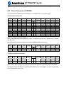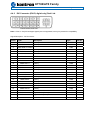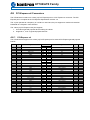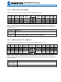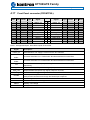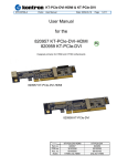
1
KT780/ATX Family KTD-00765-B Public User Manual Date: 2008-10-28 Page 1 of 77 User Manual for the Motherboards: KT780/ATX w. DVI KT780/ATX w. HDMI KT780/ATX Family KTD-00765-B Public User Manual Date: 2008-10-28 Page 2 of 77 Document revision history. Revision Date B A 0 October 28th 2008 September 18th, 2008 May. 26th, 2008 By Comment JS/MLA Minor additional information JS Revised, BIOS features added JS First preliminary manual version. Copyright Notice: Copyright © 2008, KONTRON Technology A/S, ALL RIGHTS RESERVED. No part of this document may be reproduced or transmitted in any form or by any means, electronically or mechanically, for any purpose, without the express written permission of KONTRON Technology A/S. Trademark Acknowledgement: Brand and product names are trademarks or registered trademarks of their respective owners. Disclaimer: KONTRON Technology A/S reserves the right to make changes, without notice, to any product, including circuits and/or software described or contained in this manual in order to improve design and/or performance. Specifications listed in this manual are subject to change without notice. KONTRON Technology assumes no responsibility or liability for the use of the described product(s), conveys no license or title under any patent, copyright, or mask work rights to these products, and makes no representations or warranties that these products are free from patent, copyright, or mask work right infringement, unless otherwise specified. Applications that are described in this manual are for illustration purposes only. KONTRON Technology A/S makes no representation or warranty that such application will be suitable for the specified use without further testing or modification. KT780/ATX Family KTD-00765-B Public User Manual Date: 2008-10-28 Page 3 of 77 Life Support Policy KONTRON Technology’s PRODUCTS ARE NOT FOR USE AS CRITICAL COMPONENTS IN LIFE SUPPORT DEVICES OR SYSTEMS WITHOUT EXPRESS WRITTEN APPROVAL OF THE GENERAL MANAGER OF KONTRON Technology A/S. As used herein: 1. Life support devices or systems are devices or systems which, (a) are intended for surgical implant into body, or (b) support or sustain life and whose failure to perform, when properly used in accordance with instructions for use provided in the labeling, can be reasonably expected to result in significant injury to the user. 2. A critical component is any component of a life support device or system whose failure to perform can be reasonably expected to cause the failure of the life support device or system, or to affect its safety or effectiveness. KONTRON Technology Technical Support and Services If you have questions about installing or using your KONTRON Technology Product, check this User’s Manual first – you will find answers to most questions here. To obtain support, please contact your local Distributor or Field Application Engineer (FAE). Before Contacting Support: Please be prepared to provide as much information as possible: CPU Board 1. Type. 2. Part-number. 3. Serial Number. Configuration 1. CPU Type, Clock speed. 2. DRAM Type and Size. 3. BIOS Revision (Find the Version Info in the BIOS Setup). 4. BIOS Settings different than Default Settings (Refer to the BIOS Setup Section). System 1. O/S Make and Version. 2. Driver Version numbers (Graphics, Network, and Audio). 3. Attached Hardware: Harddisks, CD-rom, LCD Panels etc. KT780/ATX Family KTD-00765-B Public User Manual Date: 2008-10-28 Page 4 of 77 Table of contents: 1. INTRODUCTION .....................................................................................................................................7 2. INSTALLATION PROCEDURE ..............................................................................................................8 2.1 Installing the board............................................................................................................................8 2.2 Requirement according to EN60950 ..............................................................................................10 3. SYSTEM SPECIFICATION ...................................................................................................................11 3.1 Component main data .....................................................................................................................11 3.2 System overview ..............................................................................................................................14 3.3 Processor support table..................................................................................................................15 3.4 System Memory support .................................................................................................................16 3.4.1 Memory Operating Frequencies .................................................................................................16 3.4.2 Memory Configurations...............................................................................................................16 4. CONNECTOR DEFINITIONS................................................................................................................18 4.1 Connector layout..............................................................................................................................19 4.1.1 KT780/ATX .................................................................................................................................19 4.2 Power Connector (ATXPWR) ..........................................................................................................21 4.3 Keyboard and PS/2 mouse connectors .........................................................................................23 4.3.1 Stacked MINI-DIN keyboard and mouse Connector (MSE & KBD) ...........................................23 4.3.2 Keyboard and mouse pin-row Connector (KBDMSE) ................................................................23 4.4 Display Connectors .........................................................................................................................24 4.4.1 CRT Connector (CRT) ................................................................................................................25 4.4.2 DVI Connector (DVI-D, digital only) Dual Link............................................................................26 4.4.3 High Definition Multimedia Interface HDMI Connector Single link. ............................................27 4.5 PCI-Express x16 Connectors..........................................................................................................28 4.5.1 PCI-Express x16.........................................................................................................................28 4.6 PCI-Express x4 Connectors............................................................................................................30 4.6.1 PCI-Express x4...........................................................................................................................30 4.7 Parallel ATA harddisk interface......................................................................................................31 4.7.1 IDE Hard Disk Connector (PATA) ..............................................................................................32 4.8 Serial ATA harddisk interface.........................................................................................................33 4.8.1 SATA Hard Disk Connector (SATA1, SATA2, SATA3, SATA4, SATA5, SATA6)......................33 4.9 Printer Port Connector (PRINTER).................................................................................................34 4.10 Serial Ports....................................................................................................................................35 4.10.1 Com1 Pin Header Connector. ....................................................................................................35 4.10.2 Com2 Pin Header Connector. ....................................................................................................35 4.11 Ethernet connectors. ...................................................................................................................36 4.11.1 Ethernet connectors (ETHER1 and ETHER2) ..........................................................................36 4.12 USB Connector (USB)..................................................................................................................37 KT780/ATX Family KTD-00765-B 4.12.1 4.12.2 4.12.3 4.12.4 4.12.5 4.12.6 Public User Manual Date: 2008-10-28 Page 5 of 77 USB Connector 0/2 (USB0/2).....................................................................................................38 USB Connector 1/3 (USB1/3).....................................................................................................38 USB Connector 4/5 (USB4/5).....................................................................................................39 USB Connector 6/7 (USB6/7).....................................................................................................39 USB Connector 8/9 (USB8/9).....................................................................................................40 USB Connector 10/11 (USB10/11).............................................................................................40 4.13 Audio Connector ..........................................................................................................................41 4.13.1 Audio Line-in, Line-out and Microphone.....................................................................................41 4.13.2 CD-ROM Audio input (CDROM).................................................................................................41 4.13.3 AUDIO Header (AUDIO_HEAD).................................................................................................42 4.14 Fan connectors , FAN_CPU, FAN_SYS, FAN_IO and FAN_NB. ..............................................43 4.15 The Clear CMOS Jumper, Clr-CMOS. .........................................................................................44 4.16 TPM connector. ............................................................................................................................44 4.17 Front Panel connector (FRONTPNL). .........................................................................................45 4.18 Feature Connector (FEATURE)...................................................................................................46 4.19 PCI Slot Connector......................................................................................................................47 4.19.1 Signal Description –PCI Slot Connector.....................................................................................48 5. SYSTEM RESOURCES ........................................................................................................................50 5.1 Memory map .....................................................................................................................................50 5.1.1 PCI devices.................................................................................................................................51 5.2 Interrupt Usage ................................................................................................................................52 5.3 I/O Map ..............................................................................................................................................53 5.4 DMA Channel Usage........................................................................................................................54 6. OVERVIEW OF BIOS FEATURES .......................................................................................................55 6.1 System Management BIOS (SMBIOS / DMI) ..................................................................................55 6.2 Legacy USB Support .......................................................................................................................55 7. BIOS CONFIGURATION / SETUP .......................................................................................................56 7.1 Introduction ......................................................................................................................................56 7.2 Main Menu.........................................................................................................................................56 7.3 Advanced Menu................................................................................................................................57 7.3.1 Advanced settings – CPU Configuration ....................................................................................57 7.3.2 Advanced settings – IDE Configuration......................................................................................58 7.3.3 Advanced settings – LAN Configuration.....................................................................................61 7.3.4 Advanced settings – Super IO Configuration .............................................................................62 7.3.5 Advanced settings – Hardware Health Configuration ................................................................63 7.3.6 Advanced settings – Voltage Monitor .........................................................................................64 7.3.7 Advanced settings – ACPI Configuration ...................................................................................64 7.3.8 Advanced settings – PCI Express Configuration........................................................................65 7.3.9 Advanced settings – USB Configuration ....................................................................................65 7.3.10 Advanced settings – USB Mass Storage Device Configuration.................................................66 7.3.11 Advanced settings – Trusted Support ........................................................................................66 KT780/ATX Family KTD-00765-B 7.4 Public User Manual Date: 2008-10-28 Page 6 of 77 PCIPnP Menu....................................................................................................................................67 7.5 Boot Menu.........................................................................................................................................68 7.5.1 Boot – Boot Settings Configuration ............................................................................................68 7.5.2 Boot – Boot Device Priority.........................................................................................................69 7.6 Security Menu...................................................................................................................................70 7.7 Chipset Menu....................................................................................................................................71 7.7.1 Advanced Chipset Settings – North Bridge Chipset Configuration ............................................71 7.7.2 Advanced Chipset Settings – Video function Configuration.......................................................72 7.7.3 Advanced Chipset Settings – SouthBridge Configuration ..........................................................73 7.8 Exit Menu ..........................................................................................................................................74 8. AMI BIOS BEEP CODES......................................................................................................................75 9. OS SETUP.............................................................................................................................................76 10. WARRANTY..........................................................................................................................................77 KT780/ATX Family KTD-00765-B Public User Manual Date: 2008-10-28 Page 7 of 77 1. Introduction This manual describes the KT780/ATX w. DVI and KT780/ATX w. HDMI boards made by KONTRON Technology A/S. The boards will also be denoted KT780 family if no differentiation is required. All boards are to be used with the AMD Phenom ™, AMD Athlon X2 64 ™, AMD Athlon X2 ™, and Sempron AM2/AM2+ socket. Use of this manual implies a basic knowledge of PC-AT hard- and software. This manual is focused on describing the KT780 Board’s special features and is not intended to be a standard PC-AT textbook. New users are recommended to study the short installation procedure stated in chapter 3 before switchingon the power. KT780/ATX Family KTD-00765-B Public User Manual Date: 2008-10-28 Page 8 of 77 2. Installation procedure 2.1 Installing the board To get the board running, follow these steps. In some cases the board shipped from KONTRON Technology has CPU, DDR2 DRAM and Cooler mounted. In this case Step 2-4 can be skipped. 1. Turn off the power supply ! Warning: Do not use Power Supply without 3.3V monitoring watchdog, which is standard feature in ATX Power Supplies. Running the board without 3.3V connected will damage the board after a few minutes. 2. Insert the DDR2 DIMM 240pin DRAM module(s) Push down the module from the top side until the tabs lock. For a list of approved DDR2 DIMM modules contact your Distributor or FAE. DDR2-667 DIMM 240pin DRAM modules (PC5300) , DDR2-800 DIMM 240pin DRAM modules (PC6400) are supported. 3. Install the processor The CPU is keyed and will only mount in the CPU socket in one way. Use the handle to open/ close the CPU socket. The AMD Phenom ™, AMD Athlon X2 64 ™, AMD Athlon X2 ™, and Sempron Processors for AM2/AM2+ socket are supported, refer to supported processor overview for details. Handle locking mechanism CPU Pin 1 marking 4. Cooler Installation A standard AM2/AM2+ CPU cooler frame is preassembled on the board, this frame is required in the combination with Kontron approved CPU Coolers. If a customer desires to used different CPU cooler, that requires a special frame the preassembled frame may be depopulated by the customer. Backside frame Cooler frame screws CPU FAN connector KT780/ATX Family KTD-00765-B Public User Manual Date: 2008-10-28 Page 9 of 77 5. Connecting Interfaces Insert all external cables for hard disk, keyboard etc. A CRT monitor must be connected in order to change CMOS settings to flat panel support. 6. Connect Power supply Connect power supply to the board by the ATX/ BTXPWR and 4-pin ATX connectors. For board to operate connection of both the ATX/BTX and 4-pin ATX (12V) connectors are required. 7. Turn on the power on the ATX/ BTX power supply 8. Power Button The PWRBTN_IN must be toggled to start the Power supply; this is done by shorting pins 16 (PWRBTN_IN) and pin 18 (GND) on the FRONTPNL connector (see Connector description). A “normally open” switch can be connected via the FRONTPNL connector. As default, activation (~ ½ sec.) of the power button makes the system toggle between turning on or shutting down. Please notice that when the button is activated in order to start shutting down sequence, the button must be release before the sequence starts, but when the button is activated in order to boot, the boot sequence start immediately when the button is activated. 9. BIOS Setup Enter the BIOS setup by pressing the <Del> key during boot up. Refer to the “BIOS Configuration / Setup“ section of this manual for details on BIOS setup. Enter Advanced Menu / CPU Configuration / Intel SpeedStep Tech. and set this option to “Maximum Performance”. Note: To clear all CMOS settings, including Password protection, move the Clr-CMOS jumper (with or without power) for approximately 1 minute. Alternatively turn off power and remove the battery for 1 minute, but be careful to orientate the battery correctly when reinserted. KT780/ATX Family KTD-00765-B Public User Manual Date: 2008-10-28 Page 10 of 77 2.2 Requirement according to EN60950 Users of KT780 boards should take care when designing chassis interface connectors in order to fulfill the EN60950 standard: When an interface/connector has a VCC (or other power) pin, which is directly connected to a power plane like the VCC plane: To protect the external power lines of peripheral devices the customer has to take care about: • That the wires have the right diameter to withstand the maximum available power. • That the enclosure of the peripheral device fulfils the fire protecting requirements of IEC/EN 60950. Lithium Battery precautions: CAUTION! VORSICHT! Danger of explosion if battery is incorrectly replaced. Explosionsgefahr bei unsachgemäßem Austausch der Batterie. Ersatz nur durch den selben oder einen vom Hersteller empfohlenen gleichwertigen Typ. Entsorgung gebrauchter Batterien nach Angaben des Herstellers. Replace only with same or equivalent type recommended by manufacturer. Dispose of used batteries according to the manufacturer’s instructions. ADVARSEL! ADVARSEL Lithiumbatteri – Eksplosionsfare ved fejlagtig håndtering. Udskiftning må kun ske med batteri af samme fabrikat og type. Levér det brugte batteri tilbage til leverandøren. Eksplosjonsfare ved feilaktig skifte av batteri. Benytt samme batteritype eller en tilsvarende type anbefalt av apparatfabrikanten. Brukte batterier kasseres i henhold til fabrikantens instruksjoner. VARNING VAROITUS Explosionsfara vid felaktigt batteribyte. Använd samma batterityp eller en ekvivalent typ som rekommenderas av apparattillverkaren. Kassera använt batteri enligt fabrikantens instruktion. Paristo voi räjähtää, jos se on virheellisesti asennettu. Vaihda paristo ainoastaan laltevalmistajan suosittelemaan tyyppiln. Hävitä käytetty paristo valmistajan ohjeiden mukaisesti. KT780/ATX Family KTD-00765-B Public User Manual Date: 2008-10-28 Page 11 of 77 3. System specification 3.1 Component main data The table below summarizes the features of the KT780 basic motherboard. Form factor Processor Memory Chipset Video Audio KT780/ATX: (305mm by 244mm / 9.6” by 12” inches) • Support for The AMD Phenom ™, AMD Athlon X2 64 ™, AMD Athlon X2 ™, and Sempron Processors for AM2/AM2+ socket. • 125W maximum TDP • 5.2GT/s HyperTransport™ link, 2600 MHz, 16bit/16bit • Hypertransport™ 1.0, 3.0 Tunnel (I/O Bus) speed of 1000MHz, 2600 MHz • Internal L1 cache of 128KB/256KB/512KB (Single core CPUs) / 128KB x2 (Dual core CPUs) • Internal L2 cache of 512KB/1024KB/2048KB (Single core CPUs) / 512KB x2 (Dual core CPUs) • Internal L3 cache (shared) of 2048KB for AMD Phenom ™ • Processor technology of 65nm / 90nm • DDR2 memory controller and bus interface • Dual Channel DDR2 memory architecture • 4 pcs DDR2 DIMM 240pin DRAM sockets onboard. • Support for DDR 533/667/800MHz unbuffered memory (PC2-4200/PC2-5300/PC26400) • Support system memory from 256MB and up to 4GB/ 32GB* (* Memory modules for support of up to 32GB may not be available) • ECC supported AMD Chipset consisting of: • AMD RS780 Northbridge ( graphics tunnel) • ATI SB700 Southbridge (I/O hub) • Integrated ATI Radeon™ HD3200 graphics core (RV610-based) o CRT Out connector o Dual link DVI-D connector (Digital only) NOTE: KT780/ATX w. DVI Board ONLY o Single link HDMI w. HDCP and Audio support NOTE: KT780/ATX w. HDMI Board ONLY • Dual independent pipe support: Mirror and Dual Independent displays supported. • Full DirectX® 10.0 support. • OpenGL 2.0 support. • Maximum resolution of 2560x1600 @ 32bpp (driver limited) for a maximum DAC speed of 400MHz. • UVD Unified Video Decoding, hardware for H.264, VC-1 and MPEG-2 decode • HW Blue Ray decoding. • HD Resolution 720p, 1080i • Sideport Video Memory of 256MB w. HDMI variant only. • Unified Memory Architecture (UMA), allowing up to 512MB dynamically allocated Video Memory (System memory is allocated when it is needed). Audio, 7.1 and 7.2 Channel High Definition Audio Codec using the Realtek ALC888 codec • Line-out • Line-in • Surround output: SIDE, LFE, CEN, BACK and FRONT • Microphone: MIC1, MIC2 • CDROM in • SPDIF Interface Onboard speaker (continues) KT780/ATX Family KTD-00765-B I/O Control Peripheral interfaces LAN Support BIOS Expansion Capabilities Hardware Monitor Subsystem Operating Systems Support Public User Manual Date: 2008-10-28 Page 12 of 77 Winbond W83627DHG LPC Bus I/O Controller • Six USB 2.0 ports on I/O area • Six USB 2.0 ports on internal pinrows • Two Serial ports (RS232) • One Parallel port, SPP/EPP/ECP • Six Serial ATA-300 IDE interfaces • PS/2 keyboard and mouse ports • 2x 10/100/1000Mbits/s LAN using Marvell 88E8055 controllers • RPL/PXE netboot supported. (Only when RAID is not selected). Wake On LAN (WOL) supported (only if +5VSB has not been lost in power down mode) • Kontron Technology / AMI BIOS (core version ??) • Support for Advanced Configuration and Power Interface (ACPI 3.0), Plug and Play o Suspend To Ram o Suspend To Disk • Secure CMOS/ OEM Setup Defaults • “Always On” BIOS power setting • RAID Support (RAID modes 0, 1, and 10) (only when PXE netboot is not selected) (for Linux O/S limitations may apply) • PCI Bus routed to PCI slots (PCI Local Bus Specification Revision 2.3) o KT780/ATX: 4 slots PCI 2.3, 32 bits, 33 MHz, 5V complying • PCI-Express bus routed to PCI Express slot(s) (PCI Express 2.0) o KT780/ATX: 1 slot PCI-Express x16 with PCI-Express x16 support • PCI-Express bus routed to PCI Express slot(s) (PCI Express 2.0) o KT780/ATX: 1 slot PCI-Express x4 with PCI-Express x4 support • SMBus routed to FEATURE, PCI slot, and PCI Express connectors • LPC Bus routed to TPM connector • DDC Bus routed to CRT,DVI connector • 8 x GPIOs (General Purpose I/Os) routed to FEATURE connector • Smart Fan control system, support Thermal® and Speed® cruise for three onboard Fan control connectors: FAN_CPU, FAN_SYS and FAN_IO. • Three thermal inputs: CPU die temperature, System temperature and External temperature. External temperature input routed to FEATURE connector. (Precision +/3ºC) • Voltage monitoring • Intrusion detect input • SMI violations (BIOS) on HW monitor not supported. Supported by API (Windows). • Windows XP, 32/64bit • Windows Vista, 32/64bit • Windows 2003, 32/64bit • WinXP Embedded (limitations may apply) • Linux: Ubuntu (limitations may apply) (continues) KT780/ATX Family KTD-00765-B Environmental Conditions Public User Manual Date: 2008-10-28 Page 13 of 77 Operating: 0°C – 50°C operating temperature (forced cooling). It is the customer’s responsibility to provide sufficient airflow around each of the components to keep them within allowed temperature range. 10% - 90% relative humidity (non-condensing) Storage: -20°C – 70°C 5% - 95% relative humidity (non-condensing) Electro Static Discharge (ESD) / Radiated Emissions (EMI): All Peripheral interfaces intended for connection to external equipment are ESD/ EMI protected. EN 61000-4-2:2000 ESD Immunity EN55022:1998 class B Generic Emission Standard. Safety: UL 60950-1:2003, First Edition CSA C22.2 No. 60950-1-03 1st Ed. April 1, 2003 Product Category: Information Technology Equipment Including Electrical Business Equipment Product Category CCN: NWGQ2, NWGQ8 File number: E194252 Theoretical MTBF: 305,732 hours / 34.9 years @25°C 209,338 hours / 23.9 years @40°C Restriction of Hazardous Substances (RoHS): All boards in the KT780 family are RoHS compliant. Capacitor utilization: No Tantalum capacitors on board Only Japanese brand Aluminum and solid electrolytic capacitors rated for 100° Celsius used on board Battery Exchangeable 3.0V Lithium battery for onboard Real Time Clock and CMOS RAM. Manufacturer Panasonic / Part-number CR2032NL/LE or CR-2032L/BE. Approximate 5 years retention. Current draw is less that 4µA when PSU is disconnected. CAUTION: Danger of explosion if the battery is incorrectly replaced. Replace only with the same or equivalent type recommended by the manufacturer. Dispose of used batteries according to the manufacturer’s instructions. KT780/ATX Family KTD-00765-B Public User Manual Date: 2008-10-28 Page 14 of 77 3.2 System overview The block diagram below shows the architecture and main components of the KT780 board. The two key components on the board are the AMD® RS780 and AMD® SB700 Embedded Chipsets. KT780/ATX Family KTD-00765-B Public User Manual Date: 2008-10-28 Page 15 of 77 3.3 Processor support table. The KT780 is designed to support the following socket AM2/AM2+ processors: AMD Phenom™ AMD Athlon 64™ AMD Athlon 64 FX™ AMD Athlon 64 x2™ AMD Sempron™ Processor Brand Clock Speed [MHz] Core] Order Number Thermal Guideline [Watt] Max. temp Embedded 2500 4 HD985ZXAJ4BGH 125W 61°C No 2300 4 HD9600WCJ4BG D 95W 70°C No 2200 4 HD9500WCJ4BG D 95W 70°C No AMD Athlon 64 X2 3200 2 ADX6400IAA6CZ 125W 63°C No AMD Athlon 64 X2 2700 2 ADO5200IAA5D0 65W 72°C No AMD Athlon 64 X2 2400 2 ADO4600IAA5DO 65W 68°C No AMD Athlon 64 1600 1 ADG2600IAV4DR 15W 70°C Yes AMD Athlon 64 1000 1 ADF2000IAV4DR 8W 70°C Yes AMD Athlon 64 X2 1800 2 ADD3600IAA5DO 35W 78°C Yes AMD Athlon 64 X2 2200 2 ADD4200IAA5DO 35W 78°C Yes AMD Sempron 2300 1 SDH1300IAA4DP 45W 79°C No AMD Sempron 2200 1 SDH1250IAA4DP 45W 79°C No AMD Phenom AMD Phenom AMD Phenom KT780/ATX Family KTD-00765-B Public User Manual Date: 2008-10-28 Page 16 of 77 3.4 System Memory support The KT780 boards have four onboard DDR2 DIMM sockets and support the following memory features: • • • • • • • • • 1.8V (only) 240-pin DDR2 SDRAM DIMMs with gold-plated contacts DDR2 800 (PC6400), DDR2 667 (PC5300) or DDR2 533 MHz (PC4200) SDRAM DIMMs DDR2 800 DIMMs with SPD timings of only 5-5-5 or 6-6-6 (tCL-tRCD-tRP) Unbuffered, single-sided or double-sided DIMMs with the following restriction: Double-sided DIMMs with x16 organization are not supported. 32 GB maximum total system memory using 64-bit OS. (Shared Video Memory is withdrawn). 4 GB maximum total system memory using 32-bit OS. ~3GB is displayed in System Properties. (Shared Video Memory is withdrawn). Minimum total system memory: 512 MB ECC DIMMs supported Serial Presence Detect The installed DDR2 SDRAM should support the Serial Presence Detect (SPD) data structure. This allows the BIOS to read and configure the memory controller for optimal performance. If non-SPD memory is used, the BIOS will attempt to configure the memory settings, but performance and reliability may be impacted. Important: If only one Memory module is used then use DDR2 SLOT 1. 3.4.1 Memory Operating Frequencies Regardless of the DIMM type used, the memory frequency depends on the processor used. For example, if DDR2 800 memory is used with a processor with lower memory frequency than 800 Mhz, the memory will operate at lower frequency. The table below lists the resulting operating memory frequencies based on the combination of DIMMs and processors. DIMM Type DDR2 533 DDR2 533 DDR2 533 DDR2 667 DDR2 667 DDR2 667 DDR2 800 DDR2 800 DDR2 800 3.4.2 Processor memory frequency 533 MHz 800 MHz 1066 MHz 533 MHz 800 MHz 1066 MHz 533 MHz 800 MHz 1066 MHz Resulting memory frequency 533 MHz 533 MHz 533 MHz 533 MHz 667 MHz 667 MHz 533 MHz 800 MHz 800 MHz Memory Configurations The KT780/ATX boards support the following three types of memory organization: Dual channel (Interleaved) mode. This mode offers the highest throughput. Dual channel mode is enabled when the installed memory capacities of both DIMM channels are equal. Technology and device width can vary from one channel to the other but the installed memory capacity for each channel must be equal. If different speed DIMMs are used between channels, the slowest memory timing will be used. Single channel (Asymmetric) mode. This mode is equivalent to single channel bandwidth operation. This mode is used when only a single DIMM is installed or the memory capacities are unequal. Technology and device width can vary from one channel to the other. If different speed DIMMs are used between channels, the slowest memory timing will be used. KT780/ATX Family KTD-00765-B Public User Manual Date: 2008-10-28 Page 17 of 77 Flex mode. This mode provides the most flexible performance characteristics. The bottommost DRAM memory (the memory that is lowest within the system memory map) is mapped to dual channel operation; the topmost DRAM memory (the memory that is nearest to the 8 GB address space limit), if any, is mapped to single channel operation. Flex mode results in multiple zones of dual and single channel operation across the whole of DRAM memory. To use flex mode, it is necessary to populate both channels. Channel A, DDR2 DIMM 0 (SLOT 1) Channel B, DDR2 DIMM 0 (SLOT 2) Channel A, DDR2 DIMM 1 (SLOT 3) Channel B, DDR2 DIMM 1 (SLOT 4) The below tables shows examples of possible Memory slot configurations for the support of the various Memory modes. Dual Channel (Interleaved) Mode Configurations Channel A Channel B DDR2 DIMM 0 (SLOT 1) DDR2 DIMM 1 (SLOT 3) DDR2 DIMM 0 (SLOT 2) DDR2 DIMM 1 (SLOT 4) 1 GB 1 GB 512 MB 512 MB 1 GB 512 MB 1 GB 512 MB 1 GB In these examples the combined capacity of the two DIMMs in Channel A equals the combined capacity of the two DIMMs in Channel B. Single Channel (Asymmetric) Mode Configurations Channel A Channel B DDR2 DIMM 0 (SLOT 1) DDR2 DIMM 1 (SLOT 3) DDR2 DIMM 0 (SLOT 2) DDR2 DIMM 1 (SLOT 4) 1 GB 512 MB 1GB 1GB In these examples the combined capacity of the two DIMMs in Channel A does not equal the capacity of the DIMMs in Channel B. KT780/ATX Family KTD-00765-B Public User Manual Date: 2008-10-28 Page 18 of 77 4. Connector Definitions The following sections provide pin definitions and detailed description of all on-board connectors. . The connector definitions follow the following notation: Column name Description Pin Shows the pin-numbers in the connector. The graphical layout of the connector definition tables is made similar to the physical connectors. Signal The mnemonic name of the signal at the current pin. The notation “XX#” states that the signal “XX” is active low. Type AI : Analog Input. AO : Analog Output. I: Input, TTL compatible if nothing else stated. IO : Input / Output. TTL compatible if nothing else stated. IOT : Bi-directional tristate IO pin. IS : Schmitt-trigger input, TTL compatible. IOC : Input / open-collector Output, TTL compatible. NC : Pin not connected. O: Output, TTL compatible. OC : Output, open-collector or open-drain, TTL compatible. OT : Output with tri-state capability, TTL compatible. LVDS: Low Voltage Differential Signal. PWR : Power supply or ground reference pins. Ioh: Typical current in mA flowing out of an output pin through a grounded load, while the output voltage is > 2.4 V DC (if nothing else stated). Iol: Typical current in mA flowing into an output pin from a VCC connected load, while the output voltage is < 0.4 V DC (if nothing else stated). Pull U/D On-board pull-up or pull-down resistors on input pins or open-collector output pins. Note Special remarks concerning the signal. The abbreviation TBD is used for specifications which are not available yet or which are not sufficiently specified by the component vendors. KT780/ATX Family KTD-00765-B Public User Manual Date: 2008-10-28 Page 19 of 77 4.1 Connector layout 4.1.1 KT780/ATX SATA6 SATA5 SATA4 SATA3 SATA2 SATA1 Feature Connector Topside, KT780/ATX: FAN_IO PATA DDR2 SLOT 4 DDR2 SLOT 3 DDR2 SLOT 2 DDR2 SLOT 1 FRONTPN Clr-CMOS AUDIO HEAD FAN_CPU TPM ATX/ BTXPWR PRINTER PCIe x16 ATX+12V *o USB8 USB9 FAN_NB ATX+12V CPU USB4 USB5 MSE KBD COM2 FAN_SYS COM1 MSE KBD CRT DVI-D HDMI* USB6 USB7 AUDIO STACK PCIe x4 CDROM PCI Slot 1,2,3,4 ETHER2 USB2 USB0 * Mounted optionally. *o Optional use. ETHER1 USB11 USB10 KT780/ATX Family KTD-00765-B Public User Manual Date: 2008-10-28 Page 20 of 77 Front, KT780/ATX MSE KBD * Mounted optionally CRT DVI-D HDMI* USB6 USB7 AUDIO STACK ETHER2 USB2 USB0 ETHER1 USB11 USB10 KT780/ATX Family KTD-00765-B Public User Manual Date: 2008-10-28 Page 21 of 77 4.2 Power Connector (ATXPWR) The KT780 boards are designed to be supplied from a standard ATX or BTX power supply. ATX/ BTX Power Connector: Note Pull U/D - Ioh/Iol - PIN - - Type PWR PWR PWR PWR I PWR PWR PWR PWR PWR PWR PWR Signal 3V3 +12V +12V SB5V P_OK GND 5V GND 5V GND 3V3 3V3 12 11 10 9 8 7 6 5 4 3 2 1 24 23 22 21 20 19 18 17 16 15 14 13 Signal GND 5V 5V 5V -5V GND GND GND PSON# GND -12V 3V3 Type PWR PWR PWR PWR PWR PWR PWR PWR OC PWR PWR PWR Ioh/Iol - Pull U/D - - - Note 1 Note 1: -5V supply is not used onboard. Note 2: Use of BTX supply not required for operation, but may be required to drive high-power PCI Express x16 Add cards. ATX+12V Power Connector (same net as +12V in ATX/BTX Power connector) : Note 1 1 Pull U/D - PIN Ioh/Iol - Type PWR PWR PWR Signal +12V +12V +12V 1 2 3 4 5 6 Signal GND GND GND Type PWR PWR PWR Ioh/Iol - Pull U/D - Type PWR Ioh/Iol - Pull U/D - PWR Note ATX+12V_CPU Power Connector: Note 1 1 Pull U/D - PIN Ioh/Iol - Type PWR PWR Signal +12V_C PU +12V_C PU 1 3 Signal GND 2 4 GND Note 1 1 Note 1: Use of the 4-pin ATX+12V_CPU Power Connector is required for operation of the KT780 boards. See chapter “Power Consumption” regarding input tolerances on 3.3V, 5V, SB5V, +12 and -12V (also refer to ATX specification version 2.2). KT780/ATX Family KTD-00765-B Public User Manual Date: 2008-10-28 Page 22 of 77 Control signal description: Signal Description P_OK P_OK is a power good signal and should be asserted high by the power supply to indicate that the +5VDC and +3.3VDC outputs are above the undervoltage thresholds of the power supply. When this signal is asserted high, there should be sufficient energy stored by the converter to guarantee continuous power operation within specification. Conversely, when the output voltages fall below the undervoltage threshold, or when mains power has been removed for a time sufficiently long so that power supply operation is no longer guaranteed, P_OK should be de-asserted to a low state. The recommended electrical and timing characteristics of the P_OK (PWR_OK) signal are provided in the ATX12V Power SupplyDesign Guide. It is strongly recommended to use an ATX or BTX supply with the KT780 boards, in order to implement the supervision of the 5V and 3V3 supplies. These supplies are not supervised onboard the KT780 boards. PS_ON# Active low open drain signal from the board to the power supply to turn on the power supply outputs. Signal must be pulled high by the power supply. KT780/ATX Family KTD-00765-B Public User Manual Date: 2008-10-28 Page 23 of 77 4.3 Keyboard and PS/2 mouse connectors Attachment of a keyboard or PS/2 mouse adapter can be done through the stacked PS/2 mouse and keyboard connector (MSE & KBD). Both interfaces utilize open-drain signaling with on-board pull-up. The PS/2 mouse and keyboard is supplied from SB5V when in standby mode in order to enable keyboard or mouse activity to bring the system out from power saving states. The supply is provided through a 1.1A resetable fuse. 4.3.1 Note Stacked MINI-DIN keyboard and mouse Connector (MSE & KBD) Pull U/D Ioh/Iol Type Signal PIN - - - NC 6 - - PWR 5V/SB5V 4 - - - NC - NC 6 4 - - PWR 5V/SB5V - - - NC 2 2 Signal Type Ioh/Iol Pull U/D 5 MSCLK IOC TBD 2K7 3 GND PWR - - MSDAT IOC TBD 2K7 5 KBDCLK IOC TBD 2K7 3 GND PWR - - KBDDAT IOC TBD 2K7 1 1 Note Signal Description – Keyboard & and mouse Connector (MSE & KBD), see below. 4.3.2 Keyboard and mouse pin-row Connector (KBDMSE) PIN 1 2 3 4 5 6 Signal KBDCLK KBDDAT MSCLK MSDAT 5V/SB5V GND Type IOC IOC IOC IOC PWR PWR Ioh/Iol TBD TBD TBD TBD - Pull U/D 4K7 4K7 4K7 4K7 - Note Signal Description – Keyboard & and mouse Connector (KBDMSE). Signal Description MSCLK Bi-directional clock signal used to strobe data/commands from/to the PS/2 mouse. MSDAT Bi-directional serial data line used to transfer data from or commands to the PS/2 mouse. KDBCLK Bi-directional clock signal used to strobe data/commands from/to the PC-AT keyboard. KBDDAT Bi-directional serial data line used to transfer data from or commands to the PC-AT keyboard. KT780/ATX Family KTD-00765-B Public User Manual Date: 2008-10-28 Page 24 of 77 4.4 Display Connectors The KT780 board provides: 1. Analog CRT interface (Front panel) 2. Digital DVI (DVI-D) (Front panel) 3. HDMI connector (Front panel) The KT780 board does not support ADD2 / SDVO cards on the PCI Express x16 connector. The KT780 integrates the ATI Radeon™ HD3200 Graphics Core with support for Dual Clone display and Dual independent display. The supported combinations are listed in the below matrix: Primary Display Secondary Display CRT CRT DVI-D Clone / Dual HDMI Clone / Dual TBD: To be determined. DVI-D HDMI Clone / Dual Clone / Dual KT780/ATX Family KTD-00765-B 4.4.1 Public User Manual Date: 2008-10-28 Page 25 of 77 CRT Connector (CRT) Note Pull U/D PIN Ioh/Iol Type Signal 6 /75R * A0 RED 1 11 7 /75R * A0 GREEN 2 12 8 /75R * A0 BLUE 3 13 9 - - - NC 4 14 10 - - PWR GND 5 15 Signal Type Ioh/Iol Pull U/D GND PWR - - NC GND DDCDAT GND HSYNC 5V VSYNC GND DDCCLK PWR IO PWR O PWR O PWR IO TBD TBD TBD TBD 6K81 - Note - 1 6K81 2 Note 1: The 5V supply in the CRT connector is fused by a 1.1A reset-able fuse. Note 2: Pull-up to +5V. Signal Description - CRT Connector: Signal Description HSYNC CRT horizontal synchronization output. VSYNC CRT vertical synchronization output. DDCCLK Display Data Channel Clock. Used as clock signal to/from monitors with DDC interface. DDCDAT Display Data Channel Data. Used as data signal to/from monitors with DDC interface. RED Analog output carrying the red color signal to the CRT. For 75 Ohm cable impedance. GREEN BLUE Analog output carrying the green color signal to the CRT. For 75 Ohm cable impedance. Analog output carrying the blue color signal to the CRT. For 75 Ohm cable impedance. DIG-GND Ground reference for HSYNC and VSYNC. ANA-GND Ground reference for RED, GREEN, and BLUE. 2 KT780/ATX Family KTD-00765-B 4.4.2 Public User Manual Date: 2008-10-28 Page 26 of 77 DVI Connector (DVI-D, digital only) Dual Link Female socket, front view Note 1: Pins C1-C5 (DVI analogue signals) are not supported, but may be present for compatibility. Signal Description - DVI Connector: Pin No. Signal Description Type Pull Up 1 TMDS Data 2- (Link 1) LVDS 2 TMDS Data 2+ (Link 1) LVDS 3 TMDS Data 2/4 Shield 4 TMDS Data 1- (Link 2) LVDS 5 TMDS Data 1+ (Link 2) LVDS 6 DDC Clock DDC Clock IO 6K8 7 DDC Data DDC Data IO 6K8 8 N.C. 9 TMDS Data 1- (Link 1) LVDS 10 TMDS Data 1+ (Link 1) LVDS 11 TMDS Data 1/3 Shield 12 TMDS Data 0- (Link 2) LVDS 13 TMDS Data 0+ (Link 2) LVDS 14 +5V PWR 15 GND PWR 16 Hot Plug Detect 17 TMDS Data 0- (Link 1) LVDS 18 TMDS Data 0+ (Link 1) LVDS 19 TMDS Data 0/5 Shield 20 TMDS Data 2- (Link 2) LVDS 21 TMDS Data 2+ (Link 2) LVDS 22 TMDS Clock Shield 23 TMDS Clock+ Digital clock + (Link 1) LVDS 24 TMDS Clock- Digital clock - (Link 1) LVDS C1 - C5 N.C. PWR - PWR Hot Plug Detect I PWR PWR - KT780/ATX Family KTD-00765-B 4.4.3 Public User Manual Date: 2008-10-28 Page 27 of 77 High Definition Multimedia Interface HDMI Connector Single link. Signal Description – HDMI Flat Panel Connector: Pin No. Signal Description Type Pull Up 1 TMDS Data 2+ LVDS 2 TMDS Data 1/3 Shield PWR 3 TMDS Data 2- LVDS 4 TMDS Data 1+ LVDS 5 TMDS Data 4/6 Shield PWR 6 TMDS Data 1- LVDS 7 TMDS Data 0+ LVDS 8 TMDS Data 7/9 Shield PWR 9 TMDS Data 0- LVDS 10 TMDS Clock+ LVDS 11 TMDS Clock Shield PWR 12 TMDS Clock- LVDS 13 N.C. - 14 N.C. - 15 DDC Clock (N.C.) DDC Clock IO 6K8 16 DDC Data (N.C.) DDC Data IO 6K8 17 GND PWR 18 +5V PWR 19 Hot Plug Detect 20 GND Hot Plug Detect I PWR KT780/ATX Family KTD-00765-B Public User Manual Date: 2008-10-28 Page 28 of 77 4.5 PCI-Express x16 Connectors The KT780 board contains one 16-lane (x16) PCI Express port on a PCI Express x16 connector. The PCI Express port is compliant to the PCI Express Specification revision 2.0. The x16 port operates at a frequency of 5.0 Gb/s on each lane; the port supports a maximum theoretical bandwidth of 16 Gbyte/s in each direction. The 16-lane (x16) PCI Express rev2 port supports: 1. An external graphics device utilizing all 16 lanes 2. Supports x4, x8 or x16 graphics devices The PCI Express port does not support SDVO and ADD2 cards. 4.5.1 PCI-Express x16 The KT780 boards supports one 16-lane (x16) PCI Express port for external PCI Express based graphics boards. Note Type Signal PIN Signal +12V +12V +12V GND SMB_CLK SMB_DATA GND +3V3 TMDS_HPD1 SB3V3 WAKE# B1 B2 B3 B4 B5 B6 B7 B8 B9 B10 B11 A1 A2 A3 A4 A5 A6 A7 A8 A9 A10 A11 COMM_EN +12V +12V GND NC DP_AUX1_P DP_AUX1_N NC +3V3 +3V3 RST# NC GND GFX_TXP[0] GFX_TXN[0] GND SC_AUX0_P GND GFX_TXP[1] GFX_TXN[1] GND GND GFX_TXP[2] GFX_TXN[2] GND GND GFX_TXP[3] GFX_TXN[3] GND NC SD_AUX0_N GND GFX_TXP[4] GFX_TXN[4] GND GND GFX_TXP[5] GFX_TXN[5] GND GND GFX_TXP[6] GFX_TXN[6] GND GND GFX_TXP[7] GFX_TXN[7] GND B12 B13 B14 B15 B16 B17 B18 B19 B20 B21 B22 B23 B24 B25 B26 B27 B28 B29 B30 B31 B32 B33 B34 B35 B36 B37 B38 B39 B40 B41 B42 B43 B44 B45 B46 B47 A12 A13 A14 A15 A16 A17 A18 A19 A20 A21 A22 A23 A24 A25 A26 A27 A28 A29 A30 A31 A32 A33 A34 A35 A36 A37 A38 A39 A40 A41 A42 A43 A44 A45 A46 A47 GND PCIE_x16 CLK PCIE_x16 CLK# GND GFX_RXP[0] GFX_RXN[0] GND NC GND GFX_RXP[1] GFX_RXN[1] GND GND GFX_RXP[2] GFX_RXN[2] GND GND GFX_RXP[3] GFX_RXN[3] GND NC NC GND GFX_RXP[4] GFX_RXN[4] GND GND GFX_RXP[5] GFX_RXN[5] GND GND GFX_RXP[6] GFX_RXN[6] GND GND GFX_RXP[7] Type Note (continues) KT780/ATX Family KTD-00765-B Public TMDS_HPD0 GND GFX_TXP[8] GFX_TXN[8] GND GND GFX_TXP[9] GFX_TXN[9] GND GND GFX_TXP[10] GFX_TXN[10] GND GND GFX_TXP[11] GFX_TXN[11] GND GND GFX_TXP[12] GFX_TXN[12] GND GND GFX_TXP[13] GFX_TXN[13] GND GND GFX_TXP[14] GFX_TXN[14] GND GND GFX_TXP[15] GFX_TXN[15] GND NC NC User Manual B48 B49 B50 B51 B52 B53 B54 B55 B56 B57 B58 B59 B60 B61 B62 B63 B64 B65 B66 B67 B68 B69 B70 B71 B72 B73 B74 B75 B76 B77 B78 B79 B80 B81 B82 Date: 2008-10-28 A48 A49 A50 A51 A52 A53 A54 A55 A56 A57 A58 A59 A60 A61 A62 A63 A64 A65 A66 A67 A68 A69 A70 A71 A72 A73 A74 A75 A76 A77 A78 A79 A80 A81 A82 GFX_RXN[7] GND NC GND GFX_RXP[8] GFX_RXN[8] GND GND GFX_RXP[9] GFX_RXN[9] GND GND GFX_RXP[10] GFX_RXN[10] GND GND GFX_RXP[11] GFX_RXN[11] GND GND GFX_RXP[12] GFX_RXN[12] GND GND GFX_RXP[13] GFX_RXN[13] GND GND GFX_RXP[14] GFX_RXN[14] GND GND GFX_RXP[15] GFX_RXN[15] GND Page 29 of 77 KT780/ATX Family KTD-00765-B Public User Manual Date: 2008-10-28 Page 30 of 77 4.6 PCI-Express x4 Connectors The KT780 board contains one 4-lane (x4) PCI Express port on a PCI Express x4 connector. The PCI Express port is compliant to the PCI Express Specification revision 2.0. The x4 port operates at a frequency of 5.0 Gb/s on each lane; the port supports a maximum theoretical bandwidth of 4 Gbyte/s in each direction. The 4-lane (x4) PCI Express rev2 port supports: 1. An external general purpose device utilizing all 4 lanes 2. Supports x1, x2 or x4 general purpose devices 4.6.1 PCI-Express x4 The KT780 boards supports one 4-lane (x4) PCI Express port for external PCI Express general purpose boards. Note Type Signal PIN Signal +12V +12V +12V GND SMB_CLK SMB_DATA GND +3V3 NC SB3V3 WAKE# B1 B2 B3 B4 B5 B6 B7 B8 B9 B10 B11 A1 A2 A3 A4 A5 A6 A7 A8 A9 A10 A11 NC +12V +12V GND NC NC NC NC +3V3 +3V3 RST# NC GND GPP_TXP[0] GPP _TXN[0] GND NC GND GPP_TXP[1] GPP_TXN[1] GND GND GPP_TXP[2] GPP_TXN[2] GND GND GPP_TXP[3] GPP_TXN[3] GND NC NC GND B12 B13 B14 B15 B16 B17 B18 B19 B20 B21 B22 B23 B24 B25 B26 B27 B28 B29 B30 B31 B32 A12 A13 A14 A15 A16 A17 A18 A19 A20 A21 A22 A23 A24 A25 A26 A27 A28 A29 A30 A31 A32 GND GPP_CLK1P GPP_CLK1N GND GPP_RXP[0] GPP_RXN[0] GND NC GND GPP_RXP[1] GPP_RXN[1] GND GND GPP_RXP[2] GPP_RXN[2] GND GND GPP_RXP[3] GPP_RXN[3] GND NC Type Note KT780/ATX Family KTD-00765-B Public User Manual Date: 2008-10-28 Page 31 of 77 4.7 Parallel ATA harddisk interface One parallel ATA harddisk controllers is available on the board – a primary controller. Standard 3½” harddisks or CD-ROM drives may be attached to the primary controller by means of the 40 pin IDC connector, PATA. The parallel ATA harddisk controller is shared between the PATA connector and the Hyperflash adapter (Accessory). Hyperflash adapter and PATA disk are not supported at the same time. The harddisk controllers support Bus master IDE, ultra DMA 33/66/100/133 MHz and standard operation modes. For support of ultra DMA 66/100/133 MHz, a 80 wire cable is required. The signals used for the harddisk interface are the following: Signal DAA2..0 HDCSA1..0# Description Address lines, used to address the I/O registers in the IDE hard disk. Hard Disk Chip-Select. HDCS0# selects the primary hard disk. DA15..8 High part of data bus. DA7..0 Low part of data bus. IORA# I/O Read. IOWA# I/O Write. IORDYA# This signal may be driven by the hard disk to extend the current I/O cycle. RESETA# Reset signal to the hard disk. HDIRQA Interrupt line from hard disk. CBLIDA This input signal (CaBLe ID) is used to detect the type of attached cable: 80-wire cable when low input and 40-wire cable when 5V via 10Kohm (pull-up resistor). DDREQA Disk DMA Request might be driven by the IDE hard disk to request bus master access to the PCI bus. The signal is used in conjunction with the PCI bus master IDE function and is not associated with any PC-AT bus compatible DMA channel. DDACKA# Disk DMA Acknowledge. Active low signal grants IDE bus master access to the PCI bus. HDACTA# Signal from hard disk indicating hard disk activity. The signal level depends on the hard disk type, normally active low. The signals from primary and secondary controller are routed together through diodes and passed to the connector FEATURE. All of the above signals are compliant to [4]. The pinout of the connectors are defined in the following sections. KT780/ATX Family KTD-00765-B 4.7.1 Public User Manual Date: 2008-10-28 Page 32 of 77 IDE Hard Disk Connector (PATA) This connector can be used for connection of two primary IDE drives. Note Pull U/D Ioh/Iol Type Signal 4K7 10K - TBD TBD TBD TBD TBD TBD TBD TBD TBD TBD TBD TBD TBD TBD - O IO IO IO IO IO IO IO IO PWR I O O I O I O O O I RESET_P# DA7 DA6 DA5 DA4 DA3 DA2 DA1 DA0 GND DDRQA IOWA# IORA# IORDYA DDACKA# HDIRQA DAA1 DAA0 HDCSA0# HDACTA# PIN 1 3 5 7 9 11 13 15 17 19 21 23 25 27 29 31 33 35 37 39 2 4 6 8 10 12 14 16 18 20 22 24 26 28 30 32 34 36 38 40 Signal Type Ioh/Iol GND DA8 DA9 DA10 DA11 DA12 DA13 DA14 DA15 KEY GND GND GND GND GND NC CBLIDA# DAA2 HDCSA1# GND PWR IO IO IO IO IO IO IO IO PWR PWR PWR PWR PWR I O O PWR TBD TBD TBD TBD TBD TBD TBD TBD TBD TBD - Pull U/D - Note KT780/ATX Family KTD-00765-B Public User Manual Date: 2008-10-28 Page 33 of 77 4.8 Serial ATA harddisk interface The KT780 boards have an integrated SATA Host controller that supports independent operation on six ports and data transfer rates of up to 3.0Gb/s (300MB/s). The SATA controller supports AHCI mode and has integrated RAID functionality with support for RAID modes 0, 1 and 10. The board provides four Serial ATA (SATA) connectors, which support one device per connector. The S700 Southbridge Serial ATA controller offers four independent Serial ATA ports with a theoretical maximum transfer rate of 3 Gbits/sec per port. A point-to-point interface is used for host to device connections, unlike Parallel ATA IDE which supports a master/slave configuration and two devices per channel. For compatibility, the underlying Serial ATA functionality is transparent to the operating system. The Serial ATA controller can operate in both legacy and native modes. In legacy mode, standard IDE I/O and IRQ resources are assigned (IRQ 14 and 15). Legacy mode is only supported on four SATA port(s). In Native mode, standard PCI Conventional bus resource steering is used. Native mode is the preferred mode for configurations using the Windows XP and Windows Vista operating systems. The KT780 supports the following RAID (Redundant Array of Independent Drives) levels: • RAID 0 - data striping • RAID 1 - data mirroring • RAID 0+1 (or RAID 10) - data striping and mirroring Limitations depending on Target Operating System apply. Note: The PCB silkscreen of SATA connectors, are not related to how the BIOS list detected devices. 4.8.1 SATA Hard Disk Connector (SATA1, SATA2, SATA3, SATA4, SATA5, SATA6) SATA: PIN Key 1 2 3 4 5 6 7 Signal Type Ioh/Iol Pull U/D GND SATA* TX+ SATA* TXGND SATA* RXSATA* RX+ GND PWR - - PWR - - PWR - - Note The signals used for the primary Serial ATA harddisk interface are the following: Signal SATA* RX+ Description Host transmitter differential signal pair SATA* RXSATA* TX+ Host receiver differential signal pair SATA* TX“*” specifies 1, 2, 3, 4, 5 and 6 depending on SATA port. All of the above signals are compliant to [6]. Note: BIOS setting ”SATA IDE Combined Mode” must be Enabled for using SATA port 5 & 6. KT780/ATX Family KTD-00765-B Public User Manual Date: 2008-10-28 Page 34 of 77 4.9 Printer Port Connector (PRINTER). The signal definition in standard printer port mode is as follows: Note Pull U/D Ioh/Iol Type Signal 2K2 2K2 2K2 2K2 2K2 2K2 2K2 2K2 2K2 2K2 2K2 2K2 2K2 (24)/24 24/24 24/24 24/24 24/24 24/24 24/24 24/24 24/24 - OC(O) IO IO IO IO IO IO IO IO I I I I STB# PD0 PD1 PD2 PD3 PD4 PD5 PD6 PD7 ACK# BUSY PE SLCT PIN 1 3 5 7 9 11 13 15 17 19 21 23 25 2 4 6 8 10 12 14 16 18 20 22 24 26 Signal Type Ioh/Iol Pull U/D AFD# ERR# INIT# SLIN# GND GND GND GND GND GND GND GND GND OC(O) I OC(O) OC(O) PWR PWR PWR PWR PWR PWR PWR PWR PWR (24)/24 (24)/24 (24)/24 - 2K2 2K2 2K2 2K2 - Note The interpretation of the signals in standard Centronics mode (SPP) with a printer attached is as follows: Signal Description PD7..0 Parallel data bus from PC board to printer. The data lines are able to operate in PS/2 compatible bi-directional mode. SLIN# Signal to select the printer sent from CPU board to printer. SLCT Signal from printer to indicate that the printer is selected. STB# This signal indicates to the printer that data at PD7..0 are valid. BUSY Signal from printer indicating that the printer cannot accept further data. ACK# Signal from printer indicating that the printer has received the data and is ready to accept further data. INIT# This active low output initializes (resets) the printer. AFD# This active low output causes the printer to add a line feed after each line printed. ERR# Signal from printer indicating that an error has been detected. PE# Signal from printer indicating that the printer is out of paper. The printer port additionally supports operation in the EPP and ECP mode as defined in [3]. KT780/ATX Family KTD-00765-B Public User Manual Date: 2008-10-28 Page 35 of 77 4.10 Serial Ports Two RS232 serial ports are available on the KT780/ATX board The typical interpretation of the signals in the COM ports is as follows: Signal Description TxD Transmitte Data, sends serial data to the communication link. The signal is set to a marking state on hardware reset when the transmitter is empty or when loop mode operation is initiated. RxD Receive Data, receives serial data from the communication link. DTR Data Terminal Ready, indicates to the modem or data set that the on-board UART is ready to establish a communication link. DSR Data Set Ready, indicates that the modem or data set is ready to establish a communication link. RTS Request To Send, indicates to the modem or data set that the on-board UART is ready to exchange data. CTS Clear To Send, indicates that the modem or data set is ready to exchange data. DCD Data Carrier Detect, indicates that the modem or data set has detected the data carrier. RI Ring Indicator, indicates that the modem has received a telephone-ringing signal. The connector pinout for each operation mode is defined in the following sections. 4.10.1 Com1 Pin Header Connector. The pinout of Serial ports Com1 is as follows: Note Pull U/D - Ioh/Iol Type Signal - I I O O PWR DCD RxD TxD DTR GND - PIN 1 3 5 7 9 2 4 6 8 10 Pull U/D Signal Type Ioh/Iol Note DSR RTS CTS RI 5V I O I I PWR - - 1 Signal Type Ioh/Iol Pull U/D Note DSR RTS CTS RI 5V I O I I PWR - - Note 1: The Com1 header 5V supply is not fused. A DB9 adapter (ribbon cable) can be used to make a DB9 pinout available. 4.10.2 Com2 Pin Header Connector. The pinout of Serial ports Com2 is as follows: Note Pull U/D - Ioh/Iol Type Signal - I I O O PWR DCD RxD TxD DTR GND - PIN 1 3 5 7 9 2 4 6 8 10 Note 1: The Com2 header 5V supply is not fused. A DB9 adapter (ribbon cable) can be used to make a DB9 pinout available. - - 1 KT780/ATX Family KTD-00765-B Public User Manual Date: 2008-10-28 Page 36 of 77 4.11 Ethernet connectors. The KT780/ATX boards supports 2 channels of 10/100/1000Mb Ethernet Marvell 88E8055 LAN controllers. In order to achieve the specified performance of the Ethernet port, Category 5 twisted pair cables must be used with 10/100MB and Category 5E, 6 or 6E with 1Gb LAN networks. The signals for the Ethernet ports are as follows: Signal Description MDI[0]+ In MDI mode, this is the first pair in 1000Base-T, i.e. the BI_DA+/- pair, and is the transmit pair in 10Base-T and 100Base-TX. MDI[0]- In MDI crossover mode, this pair acts as the BI_DB+/- pair, and is the receive pair in 10Base-T and 100Base-TX. MDI[1]- In MDI mode, this is the second pair in 1000Base-T, i.e. the BI_DB+/- pair, and is the receive pair in 10Base-T and 100Base-TX. MDI[2]+ In MDI mode, this is the third pair in 1000Base-T, i.e. the BI_DC+/- pair. MDI[2]- In MDI crossover mode, this pair acts as the BI_DD+/- pair. MDI[3]+ In MDI mode, this is the fourth pair in 1000Base-T, i.e. the BI_DD+/- pair. MDI[3]- In MDI crossover mode, this pair acts as the BI_DC+/- pair. MDI[1]+ In MDI crossover mode, this pair acts as the BI_DA+/- pair, and is the transmit pair in 10Base-T and 100Base-TX. Note: MDI = Media Dependent Interface. 4.11.1 Ethernet connectors (ETHER1 and ETHER2) Ethernet connector 1 is mounted together with USB Ports 10 and 11. Ethernet connector 2 is mounted together with USB Ports 0 and 2. The pinout of the RJ45 connector is as follows: Signal MDI0+ MDI0MDI1+ MDI2MDI1MDI2+ MDI3+ MDI3- PIN 8 7 6 5 4 Type 3 2 1 Ioh/Iol Note KT780/ATX Family KTD-00765-B Public User Manual Date: 2008-10-28 Page 37 of 77 4.12 USB Connector (USB) The KT780 boards contains two Enhanced Host Controller Interface (EHCI) host controllers that supports USB 2.0 allowing data transfers up to 480Mb/s. The KT780 boards also contains four Open Host Controller Interface (OHCI) controllers that support USB full-speed and low-speed signaling (USB 1.1). The KT780 boards supports a total of twelve USB 2.0 ports. All twelve ports are high-speed (USB 2.0), fullspeed (USB 1.1), and low-speed (USB 1.1) capable and USB Legacy mode is supported. On all USB ports SB5V is supplied during power down to allow wakeup on USB device activity. Note that in order to wakeup on USB activity a Windows XP registry file setting is required and SB5V must be applied always (no loss) during power down. Over-current detection on all ten USB ports is supported. USB Port 0 and 2 are supplied on the combined ETHER2 USB0, USB2 connector. USB Ports 1 and 3 are supplied on the internal FRONTPNL connector; please refer to the FRONTPNL connector section for the pin-out. USB Port 4 and 5 are supplied on the internal USB4, USB5 pinrow connector. USB Port 6 and 7 are supplied on the USB6, USB7 frontpanel connector. USB Port 8 and 9 are supplied on the internal USB8, USB9 pinrow connector. USB Port 10 and 11 are supplied on the combined ETHER1 USB10, USB11 connector. Note: It is recommended to use only High-/Full-Speed USB cable, specified in USB2.0 standard: KT780/ATX Family KTD-00765-B 4.12.1 Public User Manual Date: 2008-10-28 Page 38 of 77 USB Connector 0/2 (USB0/2) USB Port 0 and 2 are supplied on the combined ETHER2 USB0, USB2 connector. Note Pull U/D Ioh/Iol Type Signal 1 1 /15K 0.25/2 PWR IO /15K 0.25/2 PWR IO 2 Signal Type Ioh/Iol Pull U/D GND USB2+ PWR IO 0.25/2 /15K GND USB0+ PWR IO 0.25/2 /15K Note 4 5V/SB5V USB21 1 PIN 2 3 3 4 5V/SB5V USB0- Note 1: The 5V supply for the USB devices is on-board fused with a 2.0A reset-able fuse. The supply is common for the two channels. In order to meet the requirements of USB standard, the 5V input supply must be at least 5.00V. Signal USB2+ USB2- Description Differential pair works as Data/Address/Command Bus. USB0+ USB0USB5V 4.12.2 5V supply for external devices. Fused with 2.0A reset-able fuse. USB Connector 1/3 (USB1/3) USB Ports 1 and 3 are supplied on the internal FRONTPNL connector; please refer to the FRONTPNL connector section for the pin-out. Note Pull U/D 1 - Ioh/Iol Type Signal - PWR IO IO PWR 5V/SB5V USB1USB1+ GND KEY - PIN 1 3 5 7 9 2 4 6 8 10 Signal Type Ioh/Iol 5V/SB5V USB3USB3+ GND LINE2-L PWR IO IO PWR - Pull U/D Note 1 - - Note 1: The 5V supply for the USB devices is on-board fused with a 2.0A reset-able fuse. The supply is common for the two channels. In order to meet the requirements of USB standard, the 5V input supply must be at least 5.00V. Signal USB1+ USB1- Description Differential pair works as Data/Address/Command Bus. USB3+ USB3USB5V 5V supply for external devices. Fused with 2.0A reset-able fuse. KT780/ATX Family KTD-00765-B 4.12.3 Public User Manual Date: 2008-10-28 Page 39 of 77 USB Connector 4/5 (USB4/5) USB Port 4 and 5 are supplied on the internal USB4, USB5 pinrow connector. Note Pull U/D 1 - Ioh/Iol Type Signal - PWR IO IO PWR 5V/SB5V USB4USB4+ GND KEY - PIN 1 3 5 7 9 2 4 6 8 10 Signal Type Ioh/Iol 5V/SB5V USB5USB5+ GND NC PWR IO IO PWR - Pull U/D Note 1 - - Note 1: The 5V supply for the USB devices is on-board fused with a 2.0A reset-able fuse. The supply is common for the two channels. In order to meet the requirements of USB standard, the 5V input supply must be at least 5.00V. Signal USB4+ USB4- Description Differential pair works as Data/Address/Command Bus. USB5+ USB5USB5V 4.12.4 5V supply for external devices. Fused with 2.0A reset-able fuse. USB Connector 6/7 (USB6/7) USB Port 6 and 7 are supplied on the USB6, USB7 frontpanel connector. Note Pull U/D Ioh/Iol Type Signal 1 1 /15K 0.25/2 PWR IO 5V/SB5V USB6- 1 /15K 0.25/2 PWR IO 5V/SB5V USB7- 1 PIN 2 3 2 3 Signal Type Ioh/Iol Pull U/D GND USB6+ PWR IO 0.25/2 /15K GND USB7+ PWR IO 0.25/2 /15K Note 4 4 Note 1: The 5V supply for the USB devices is on-board fused with a 2.0A reset-able fuse. The supply is common for the two channels. In order to meet the requirements of USB standard, the 5V input supply must be at least 5.00V. Signal USB6+ USB6- Description Differential pair works as Data/Address/Command Bus. USB7+ USB7USB5V 5V supply for external devices. Fused with 2.0A reset-able fuse. KT780/ATX Family KTD-00765-B 4.12.5 Public User Manual Date: 2008-10-28 Page 40 of 77 USB Connector 8/9 (USB8/9) USB Port 8 and 9 are supplied on the internal USB8, USB9 pinrow connector. Pull U/D Note Ioh/Iol Type Signal - PWR IO IO PWR 5V/SB5V USB8USB8+ GND KEY 1 - - PIN 1 3 5 7 9 2 4 6 8 10 Signal Type Ioh/Iol 5V/SB5V USB9USB9+ GND NC PWR IO IO PWR - Pull U/D Note 1 - - Note 1: The 5V supply for the USB devices is on-board fused with a 2.0A reset-able fuse. The supply is common for the two channels. In order to meet the requirements of USB standard, the 5V input supply must be at least 5.00V. Signal USB8+ USB8- Description Differential pair works as Data/Address/Command Bus. USB9+ USB9USB5V 4.12.6 5V supply for external devices. Fused with 2.0A reset-able fuse. USB Connector 10/11 (USB10/11) USB Port 10 and 11 are supplied on the combined ETHER1 USB10, USB11 connector. Pull U/D Ioh/Iol Type Signal 1 /15K 0.25/2 PWR IO 5V/SB5V USB11- 1 /15K 0.25/2 PWR IO 5V/SB5V USB10- Note 1 1 PIN 2 3 2 3 Signal Type Ioh/Iol Pull U/D GND USB11+ PWR IO 0.25/2 /15K GND USB10+ PWR IO 0.25/2 /15K Note 4 4 Note 1: The 5V supply for the USB devices is on-board fused with a 2.0A reset-able fuse. The supply is common for the two channels. In order to meet the requirements of USB standard, the 5V input supply must be at least 5.00V. Signal USB11+ USB11- Description Differential pair works as Data/Address/Command Bus. USB10+ USB10USB5V 5V supply for external devices. Fused with 2.0A reset-able fuse. KT780/ATX Family KTD-00765-B Public User Manual Date: 2008-10-28 Page 41 of 77 4.13 Audio Connector The onboard Audio circuit implements 7.1+2 Channel High Definition Audio, featuring ten 24-bit stereo DACs and two 20-bit stereo ADCs. The Audio signals are made available on the Frontpanel stacked connector (Line in / Line out / MIC) and the onboard AUDIO_HEAD and CDROM Audio input connectors. 4.13.1 Audio Line-in, Line-out and Microphone Audio Line-in, Line-out and Microphone are available in the stacked audio jack connector. IN Signal Type Note TIP RING SLEEVE LINE1-IN-L LINE1-IN-R GND IA IA PWR 1 1 TIP RING SLEEVE FRONT-OUT-L FRONT-OUT-R GND OA OA PWR TIP RING SLEEVE MIC1-L MIC1-R GND IA IA PWR 1 1 Note 1: Signals are shorted to GND internally in the connector, when jack-plug not inserted. 4.13.2 CD-ROM Audio input (CDROM) CD-ROM audio input may be connected to this connector. It may also be used as a secondary line-in signal. PIN Signal Type Ioh/Iol 1 2 3 4 CD_Left CD_GND CD_GND CD_Right IA IA IA IA - Pull U/D - Note 1 1 Note 1: The definition of which pins are use for the Left and Right channels is not a worldwide accepted standard. Some CDROM cable kits expect reverse pin order. Signal Description CD_Left CD_Right Left and right CD audio input lines or secondary Line-in. CD_GND Analogue GND for Left and Right CD. (This analogue GND is not shorted to the general digital GND on the board). Note: To make the CD-ROM Audio input play, open Realtek audio software-Mixer, select Tool (in left corner) and select "Advanced playback of multi streaming". KT780/ATX Family KTD-00765-B 4.13.3 Note Public User Manual Date: 2008-10-28 Page 42 of 77 AUDIO Header (AUDIO_HEAD) Pull U/D Ioh/ Iol - - Signal Type PWR Signal LFE-OUT AAGND FRONT-OUT-L AAGND REAR-OUT-L SIDE-OUT-L AAGND MIC1-L AAGND LINE1-IN-L NC GND SPDIF-OUT PIN 1 3 5 7 9 11 13 15 17 19 21 23 25 2 4 6 8 10 12 14 16 18 20 22 24 26 Signal CEN-OUT AAGND FRONT-OUT-R AAGND REAR-OUT-R SIDE-OUT-R AAGND MIC1-R AAGND LINE1-IN-R AAGND SPDIF-IN GND Description FRONT-OUT-L Front Speakers (Speaker Out Left). FRONT-OUT-R Front Speakers (Speaker Out Right). REAR-OUT-L Rear Speakers (Surround Out Left). REAR-OUT-R Rear Speakers (Surround Out Right). SIDE-OUT-L Side speakers (Surround Out Left) SIDE-OUT-R Side speakers (Surround Out Right) CEN-OUT Center Speaker (Center Out channel). LFE-OUT Subwoofer Speaker (Low Freq. Effect Out). NC MIC1 LINE1-IN F-SPDIF-IN F-SPDIF-OUT AAGND No connection MIC Input 1 Line in 1 signals S/PDIF Input S/PDIF Output Audio Analogue ground Note Type PWR Ioh/ Iol Pull U/D - - Note KT780/ATX Family KTD-00765-B Public User Manual Date: 2008-10-28 Page 43 of 77 4.14 Fan connectors , FAN_CPU, FAN_SYS, FAN_IO and FAN_NB. The FAN_CPU is used for connection of the active cooler for the CPU. The FAN_SYS can be used to power, control and monitor a fan for chassis ventilation etc. The FAN_IO can be used to power, control and monitor a fan for chassis ventilation etc. The FAN_NB is used for connection of the active cooler for the North bridge (Optional, 3-pin only). The 4pin header supports connection of 3-pin FANs, but it is recommended to use the 4-pin type for optimized FAN speed control. The 3- or 4-pin mode is controlled in the BIOS setup menu. 4-pin Mode: PIN 1 2 3 4 Signal CONTROL SENSE Signal CONTROL SENSE +12 V GND Type O I PWR PWR Ioh/Iol - Pull U/D Note 4K7 to 12V - Description PWM signal for FAN speed control Tacho signal input with on board pull-up resistor 4K7 to +12V. The signal has to be pulses, typically 2 Hz per rotation. 12V +12V supply for fan. A maximum of 2000 mA can be supplied from this pin. GND Power Supply GND signal 3-pin Mode: PIN Signal 2 3 4 SENSE +12 V GND Type I PWR PWR Ioh/Iol - Pull U/D Note 4K7 to 12V - Signal Description SENSE Tacho signal input with on board pull-up resistor 4K7 to +12V. The signal has to be pulses, typically 2 Hz per rotation. +12V supply for fan, can be turned on/off or modulated (PWM) by the chipset. A maximum of 2000 mA can be supplied from this pin. Power Supply GND signal 12V GND 3-pin Native for North bridge: PIN 1 2 3 Signal SENSE +12 V GND Type I PWR PWR Ioh/Iol - Pull U/D Note 4K7 to 12V - Signal Description SENSE Tacho signal input with on board pull-up resistor 4K7 to +12V. The signal has to be pulses, typically 2 Hz per rotation. +12V supply for fan, can be turned on/off or modulated (PWM) by the chipset. A maximum of 2000 mA can be supplied from this pin. Power Supply GND signal 12V GND KT780/ATX Family KTD-00765-B Public User Manual Date: 2008-10-28 Page 44 of 77 4.15 The Clear CMOS Jumper, Clr-CMOS. The Clr-CMOS Jumper is used to clear the CMOS content. ↑ CPU location ↑ No Jumper installed 1 2 3 • Jumper normal position Jumper in Clear CMOS position (Pin numbers) • To clear all CMOS settings, including Password protection, move the CMOS_CLR jumper (with or without power on the system) for approximately 1 minute. Alternatively if no jumper is available, turn off power and remove the battery for 1 minute, but be careful to orientate the battery correctly when reinserted. 4.16 TPM connector. Note: The KT780 board have integrated TPM device. Note Pull U/D - Ioh/Iol - Type PWR PWR Signal LPC CLK LPC FRAME# LPC RST# LPC AD3 +3V3 LPC AD0 SMB_CLK SB3V3 GND SUS_STAT# PIN 1 3 5 7 9 11 13 15 17 19 2 6 8 10 12 14 16 18 20 Signal GND KEY +5V LPC AD2 LPC AD1 GND SMB_DATA LPC SERIRQ CLKRUN# LPC IRQ# Type Ioh/Iol Pull U/D Note KT780/ATX Family KTD-00765-B Public User Manual Date: 2008-10-28 Page 45 of 77 4.17 Front Panel connector (FRONTPNL). Note Pull U/D Ioh/Iol - - - - 1 Type PWR PWR OC PWR Signal USB13_5V USB1USB1+ GND KEY +5V HD_LED GND RSTIN# SB3V3 AGND MIC2-L PIN 1 3 5 7 11 13 15 17 19 21 23 2 4 6 8 10 12 14 16 18 20 22 24 Signal USB13_5V USB3USB3+ GND LINE2-IN-L +5V SUS_LED PWRBTN_IN# GND LINE2-IN-R AGND MIC2-R Type Ioh/Iol Pull U/D PWR PWR - - PWR - - - Note 1 Note 1: Unsupported inputs, leave these inputs unconnected. Signal USB13_5V USB1+ USB1USB3+ USB3+5V HD_LED SUS_LED Description +5V supply for the USB devices on USB Port 1 and 3 is on-board fused with a 1.5A reset-able fuse. The supply is common for the two channels. Universal Serial Bus Port 1 Differentials: Bus Data/Address/Command Bus. Universal Serial Bus Port 3 Differentials: Bus Data/Address/Command Bus. Maximum load is 1A or 2A per pin if using IDC connector flatcable or crimp terminals respectively. Hard Disk Activity LED (active low signal). Output is via 475Ω to OC. Suspend Mode LED (active high signal). Output is via 475Ω. PWRBTN_IN# Power Button In. Toggle this signal low to start the ATX / BTX PSU and boot the board. RSTIN# Reset Input. When pulled low for minimum 16mS the reset process will be initiated. The reset process continues even though the Reset Input is kept low. LINE2-IN Line in 2 signals MIC2 MIC2-L and MIC2-R are unsupported. Leave these terminals unconnected. SB3V3 Standby 3.3V voltage AGND Analogue Ground for Audio KT780/ATX Family KTD-00765-B Public User Manual Date: 2008-10-28 Page 46 of 77 4.18 Feature Connector (FEATURE) Pull PIN Signal Signal Type Ioh/Iol U/D Note INTRUDER# 1 2 GND PWR EXT_ISAIRQ# 3 4 EXT_SMI# I PWR_OK 5 6 SB5V PWR PWR SB3V3 7 8 EXT_BAT PWR PWR +5V 9 10 GND PWR 1 4K7/ /12mA IOT GPIO0 11 12 GPIO1 IOT /12mA 2K7/ 1 1 4K7/ /12mA IOT GPIO2 13 14 GPIO3 IOT /12mA 2K7/ 1 1 4K7/ /12mA IOT GPIO4 15 16 GPIO5 IOT /12mA 2K7/ 3 3 4K7/ /12mA IOT GPIO6 17 18 GPIO7 IOT /12mA 2K7/ 3 PWR GND 19 20 FAN3OUT FAN3IN 21 22 +12V PWR TEMP3IN 23 24 VREF PWR GND 25 26 IRRX IRTX 27 28 GND PWR 1 2K7/ SMBC 29 30 SMBD 2K7/ 1 Note 1: Pull-up to +3V3Dual (+3V3 or SB3V3). Note 2: Pull-up to RTC-Voltage. Note 3: Pull-up to +3V3. Note 2 Pull U/D 2M/ Signal INTRUDER# EXT_ISAIRQ# Ioh/Iol - Type I Description INTRUDER, may be used to detect if the system case has been opened. This signal’s status is readable, so it may be used like a GPI when the Intruder switch is not needed. EXTernal ISA IRQ, (active low input) can activate standard AT-Bus IRQ-interrupt. EXT_SMI# External SMI, (active low input) signal can activate SMI interrupt. PWR_OK PoWeR OK, signal is high if no power failures is detected. SB5V StandBy +5V supply. SB3V3 Max. load is 0.75A (1.5A < 1 sec.) (EXTernal BATtery) the + terminal of an external primary cell battery can be connected to this pin. The – terminal of the battery shall be connected to GND (etc. pin 10). The external battery is protected against charging and can be used with or without the on board battery installed. The external battery voltage shall be in the range: 2.5 - 4.0 V DC. Current draw is 3µA when PSU is disconnected. Max. load is 0.75A (1.5A < 1 sec.) General Purpose Inputs / Output. These Signals may be controlled or monitored through the use of the KONTRON API (Application Programming Interface) available for WinXP and Windows Vista. FAN 3 speed control OUTput. This analogue voltage output signal can be set to output voltages from 0 – 3V3 to control the Fan’s speed.. For more information please look into the datasheet for the Winbond I/O controller W83627. EXT_BAT +5V GPIO0..7 FAN3OUT FAN3IN +12V FAN3 Input. 0V to +3V3 amplitude Fan 3 tachometer input. VREF Max. load is 0.75A (1.5A < 1 sec.) Temperature sensor 3 input. (Recommended: Transistor 2N3904, having emitter connected to GND (pin 25), collector and basis shorted and connected to pin23 (Temp3In). Further a resistor 30K/1% shall be connected between pin 23 and pin 24 (Vref). (Precision +/- 3ºC) Voltage REFerence, reference voltage to be used with TEMP3IN input. IRRX IR Receive input (IrDA 1.0, SIR up to 1.152K bps) IRTX IR Transmit output (IrDA 1.0, SIR up to 1.152K bps) TEMP3IN SMBC SMBus Clock signal SMBD SMBus Data signal KT780/ATX Family KTD-00765-B 4.19 Public User Manual Date: 2008-10-28 Page 47 of 77 PCI Slot Connector Terminal Note Type Signal S C Signal Type PWR O PWR -12V TCK GND NC +5V +5V INTB# INTD# NC NC NC GND GND NC GND PCICLK GND REQ0# +5V (I/O) AD31 AD29 GND AD27 AD25 +3.3V C/BE3# AD23 GND AD21 AD19 +3.3V AD17 C/BE2# GND IRDY# +3.3V DEVSEL# GND LOCK# PERR# +3.3V SERR# +3.3V C/BE1# AD14 GND AD12 AD10 GND F01 F02 F03 F04 F05 F06 F07 F08 F09 F10 F11 F12 F13 F14 F15 F16 F17 F18 F19 F20 F21 F22 F23 F24 F25 F26 F27 F28 F29 F30 F31 F32 F33 F34 F35 F36 F37 F38 F39 F40 F41 F42 F43 F44 F45 F46 F47 F48 F49 E01 E02 E03 E04 E05 E06 E07 E08 E09 E10 E11 E12 E13 E14 E15 E16 E17 E18 E19 E20 E21 E22 E23 E24 E25 E26 E27 E28 E29 E30 E31 E32 E33 E34 E35 E36 E37 E38 E39 E40 E41 E42 E43 E44 E45 E46 E47 E48 E49 TRST# +12V TMS TDI +5V INTA# INTC# +5V NC +5V (I/O) NC GND GND 3V3 RST# +5V (I/O) GNT0# GND PME# AD30 +3.3V AD28 AD26 GND AD24 IDSEL +3.3V AD22 AD20 GND AD18 AD16 +3.3V FRAME# GND TRDY# GND STOP# +3.3V SMB_CLK SMB_DATA GND PAR AD15 +3.3V AD13 AD11 GND AD09 O PWR O O PWR I I PWR F52 F53 F54 F55 F56 F57 F58 F59 F60 F61 F62 E52 E53 E54 E55 F56 E57 E58 E59 E60 E61 E62 C/BE0# +3.3V AD06 AD04 GND AD02 AD00 +5V (I/O) REQ64# +5V +5V PWR PWR I I PWR PWR PWR O PWR I PWR IOT IOT PWR IOT IOT PWR IOT IOT PWR IOT IOT PWR IOT IOT PWR IOT PWR IOT PWR IOT IOT PWR IOC PWR IOT IOT PWR IOT IOT PWR SOLDER SIDE 8K2/ PU IOT IOT PWR IOT IOT PWR IOT PWR IOT PWR PWR AD08 AD07 +3.3V AD05 AD03 GND AD01 +5V (I/O) ACK64# +5V +5V Note PWR O PWR PWR OT O PWR OT PWR O IOT PWR IOT IOT PWR IOT IOT PWR IOT IOT PWR IOT IOT PWR IOT PWR IOT PWR IOT PWR IO IO PWR IOT IOT PWR IOT IOT PWR IOT COMPONENT SIDE IOT PWR IOT IOT PWR IOT IOT PWR IOT PWR PWR 8K2/ PU KT780/ATX Family KTD-00765-B 4.19.1 Public User Manual Date: 2008-10-28 Page 48 of 77 Signal Description –PCI Slot Connector SYSTEM PINS Clock provides timing for all transactions on PCI and is an input to every PCI device. All other PCI signals, CLK except RST#, INTA#, INTB#, INTC#, and INTD#, are sampled on the rising edge of CLK and all other timing parameters are defined with respect to this edge. PCI operates at 33 MHz. Reset is used to bring PCI-specific registers, sequencers, and signals to a consistent state. What effect RST# RST# has on a device beyond the PCI sequencer is beyond the scope of this specification, except for reset states of required PCI configuration registers. Anytime RST# is asserted, all PCI output signals must be driven to their benign state. In general, this means they must be asynchronously tri-stated. SERR# (open drain) is floated. REQ# and GNT# must both be tri-stated (they cannot be driven low or high during reset). To prevent AD, C/BE#, and PAR signals from floating during reset, the central resource may drive these lines during reset (bus parking) but only to a logic low level–they may not be driven high. RST# may be asynchronous to CLK when asserted or deasserted. Although asynchronous, deassertion is guaranteed to be a clean, bounce-free edge. Except for configuration accesses, only devices that are required to boot the system will respond after reset. ADDRESS AND DATA Address and Data are multiplexed on the same PCI pins. A bus transaction consists of an address phase AD[31::00] followed by one or more data phases. PCI supports both read and write bursts. The address phase is the clock cycle in which FRAME# is asserted. During the address phase AD[31::00] contain a physical address (32 bits). For I/O, this is a byte address; for configuration and memory, it is a DWORD address. During data phases AD[07::00] contain the least significant byte (lsb) and AD[31::24] contain the most significant byte (msb). Write data is stable and valid when IRDY# is asserted and read data is stable and valid when TRDY# is asserted. Data is transferred during those clocks where both IRDY# and TRDY# are asserted. C/BE[3::0]# Bus Command and Byte Enables are multiplexed on the same PCI pins. During the address phase of a transaction, C/BE[3::0]# define the bus command. During the data phase C/BE[3::0]# are used as Byte Enables. The Byte Enables are valid for the entire data phase and determine which byte lanes carry meaningful data. C/BE[0]# applies to byte 0 (lsb) and C/BE[3]# applies to byte 3 (msb). Parity is even parity across AD[31::00] and C/BE[3::0]#. Parity generation is required by all PCI agents. PAR PAR is stable and valid one clock after the address phase. For data phases, PAR is stable and valid one clock after either IRDY# is asserted on a write transaction or TRDY# is asserted on a read transaction. Once PAR is valid, it remains valid until one clock after the completion of the current data phase. (PAR has the same timing as AD[31::00], but it is delayed by one clock.) The master drives PAR for address and write data phases; the target drives PAR for read data phases. INTERFACE CONTROL PINS Cycle Frame is driven by the current master to indicate the beginning and duration of an access. FRAME# FRAME# is asserted to indicate a bus transaction is beginning. While FRAME# is asserted, data transfers continue. When FRAME# is deasserted, the transaction is in the final data phase or has completed. Initiator Ready indicates the initiating agent’s (bus master’s) ability to complete the current data phase of IRDY# the transaction. IRDY# is used in conjunction with TRDY#. A data phase is completed on any clock both IRDY# and TRDY# are sampled asserted. During a write, IRDY# indicates that valid data is present on AD[31::00]. During a read, it indicates the master is prepared to accept data. Wait cycles are inserted until both IRDY# and TRDY# are asserted together. Target Ready indicates the target agent’s (selected device’s) ability to complete the current data phase of TRDY# the transaction. TRDY# is used in conjunction with IRDY#. A data phase is completed on any clock both TRDY# and IRDY# are sampled asserted. During a read, TRDY# indicates that valid data is present on AD[31::00]. During a write, it indicates the target is prepared to accept data. Wait cycles are inserted until both IRDY# and TRDY# are asserted together. Stop indicates the current target is requesting the master to stop the current transaction. STOP# Lock indicates an atomic operation that may require multiple transactions to complete. When LOCK# is LOCK# asserted, non-exclusive transactions may proceed to an address that is not currently locked. A grant to start a transaction on PCI does not guarantee control of LOCK#. Control of LOCK# is obtained under its own protocol in conjunction with GNT#. It is possible for different agents to use PCI while a single master retains ownership of LOCK#. If a device implements Executable Memory, it should also implement LOCK# and guarantee complete access exclusion in that memory. A target of an access that supports LOCK# must provide exclusion to a minimum of 16 bytes (aligned). Host bridges that have system memory behind them should implement LOCK# as a target from the PCI bus point of view and optionally as a master. Initialization Device Select is used as a chip select during configuration read and write transactions. IDSEL Device Select, when actively driven, indicates the driving device has decoded its address as the target of DEVSEL# the current access. As an input, DEVSEL# indicates whether any device on the bus has been selected. (continues) KT780/ATX Family KTD-00765-B Public User Manual Date: 2008-10-28 Page 49 of 77 ARBITRATION PINS (BUS MASTERS ONLY) Request indicates to the arbiter that this agent desires use of the bus. This is a point to point signal. Every REQ# master has its own REQ# which must be tri-stated while RST# is asserted. Grant indicates to the agent that access to the bus has been granted. This is a point to point signal. Every GNT# master has its own GNT# which must be ignored while RST# is asserted. While RST# is asserted, the arbiter must ignore all REQ# lines since they are tri-stated and do not contain a valid request. The arbiter can only perform arbitration after RST# is deasserted. A master must ignore its GNT# while RST# is asserted. REQ# and GNT# are tri-state signals due to power sequencing requirements when 3.3V or 5.0V only add-in boards are used with add-in boards that use a universal I/O buffer. ERROR REPORTING PINS. The error reporting pins are required by all devices and maybe asserted when enabled Parity Error is only for the reporting of data parity errors during all PCI transactions except a Special Cycle. PERR# The PERR# pin is sustained tri-state and must be driven active by the agent receiving data two clocks following the data when a data parity error is detected. The minimum duration of PERR# is one clock for each data phase that a data parity error is detected. (If sequential data phases each have a data parity error, the PERR# signal will be asserted for more than a single clock.) PERR# must be driven high for one clock before being tri-stated as with all sustained tri-state signals. There are no special conditions when a data parity error may be lost or when reporting of an error may be delayed. An agent cannot report a PERR# until it has claimed the access by asserting DEVSEL# (for a target) and completed a data phase or is the master of the current transaction. System Error is for reporting address parity errors, data parity errors on the Special Cycle command, or SERR# any other system error where the result will be catastrophic. If an agent does not want a non-maskable interrupt (NMI) to be generated, a different reporting mechanism is required. SERR# is pure open drain and is actively driven for a single PCI clock by the agent reporting the error. The assertion of SERR# is synchronous to the clock and meets the setup and hold times of all bused signals. However, the restoring of SERR# to the deasserted state is accomplished by a weak pullup (same value as used for s/t/s) which is provided by the system designer and not by the signaling agent or central resource. This pull-up may take two to three clock periods to fully restore SERR#. The agent that reports SERR#s to the operating system does so anytime SERR# is sampled asserted. INTERRUPT PINS (OPTIONAL). Interrupts on PCI are optional and defined as “level sensitive,” asserted low (negative true), using open drain output drivers. The assertion and deassertion of INTx# is asynchronous to CLK. A device asserts its INTx# line when requesting attention from its device driver. Once the INTx# signal is asserted, it remains asserted until the device driver clears the pending request. When the request is cleared, the device deasserts its INTx# signal. PCI defines one interrupt line for a single function device and up to four interrupt lines for a multi-function device or connector. For a single function device, only INTA# may be used while the other three interrupt lines have no meaning. Interrupt A is used to request an interrupt. INTA# Interrupt B is used to request an interrupt and only has meaning on a multi-function device. INTB# INTC# Interrupt C is used to request an interrupt and only has meaning on a multi-function device. INTD# Interrupt D is used to request an interrupt and only has meaning on a multi-function device. KT780/ATX Family KTD-00765-B Public User Manual Date: 2008-10-28 Page 5. System Resources 5.1 Memory map Address range (hex) 00000000 0009FFFF 000A0000 000BFFFF 000A0000 000BFFFF 000A0000 000BFFFF 000C0000 000CFFFF 000D0000 000DFFFF 000E0000 000FFFFF 00100000 6FFFFFFF 70000000 7FFFFFFF 70000000 DFFFFFFF D0000000 DFFFFFFF D0000000 DFFFFFFF E0000000 EFFFFFFF F0000000 FEBFFFFF FE7CC000 FE7CFFFF FE7DA000 FE7DAFFF FE7DB000 FE7DBFFF FE7F0000 FE7F0FFF FE7F1000 FE7F1FFF FE7F2000 FE7F2FFF FE7F3400 FE7F34FF FE7F3800 FE7F38FF FE7F3C00 FE7F3FFF FE800000 FE8FFFFF FE800000 FE9FFFFF FE9E8000 FE9EBFFF FE9F0000 FE9FFFFF FEA00000 FEAFFFFF FEAFC000 FEAFFFFF FEB00000 FEBFFFFF FEBFC000 FEBFFFFF FEC00000 FEC00FFF FEC00000 FFFFFFFF FEC10000 FEC1001F FED00000 FED003FF FEE00000 FEE00FFF FFB80000 FFBFFFFF Size (bytes) 655360 131072 131072 131072 65536 65536 131072 1877999616 268435456 1879048192 268435456 268435456 268435456 247463936 16384 4096 4096 4096 4096 4096 256 256 1024 1048576 2097152 16384 65536 1048576 16384 1048576 16384 4096 20971520 32 1024 4096 524288 Description System board ATI Radeon HD 3200 Graphics PCI standard PCI to PCI-Bridge PCI-bus System board PCI-bus System board System board (2 GB Memory – VGA Memory) Motherboard resources PCI-bus ATI Radeon HD 3200 Graphics PCI standard PCI to PCI-Bridge Motherboard resources PCI-bus Microsoft UAA Bus Driver for High Definition Audio Standard OpenHCD USB Host Controller Standard OpenHCD USB Host Controller Standard OpenHCD USB Host Controller Standard OpenHCD USB Host Controller Standard OpenHCD USB Host Controller Standard Enhanced PCI to USB Host Controller Standard Enhanced PCI to USB Host Controller Standard Dual Channel PCI IDE-controller ATI Radeon HD 3200 Graphics PCI standard PCI to PCI-Bridge Microsoft UAA Bus Driver for High Definition Audio ATI Radeon HD 3200 Graphics PCI standard PCI to PCI-Bridge Marvell Yukon 88E8055 PCI-E Gigabit Ethernet PCI standard PCI to PCI-Bridge Marvell Yukon 88E8055 PCI-E Gigabit Ethernet Motherboard resources System board Motherboard resources High precision event timer Motherboard resources Motherboard resources Notes: This is the memory map after a standard Windows XP SP2 installation 50 of 77 KT780/ATX Family KTD-00765-B 5.1.1 Bus # 0 0 0 0 0 0 0 0 0 0 0 0 0 0 0 0 0 0 0 0 0 0 1 1 2 3 4 4 4 4 Public User Manual Date: 2008-10-28 Page 51 of 77 PCI devices Device # 0 1 9 10 17 18 18 18 19 19 19 20 20 20 20 20 20 24 24 24 24 24 5 5 0 0 5 6 7 8 Function # 0 0 0 0 0 0 1 2 0 1 2 0 1 2 3 4 5 0 1 2 3 4 0 1 0 0 Vendor ID 1022h 1022h 1022h 1022h 1002h 1002h 1002h 1002h 1002h 1002h 1002h 1002h 1002h 1002h 1002h 1002h 1002h 1022h 1022h 1022h 1022h 1022h 1002h 1002h 11ABh 11ABh - Device ID 9600h 9602h 9608h 9609h 4390h 4397h 4398h 4396h 4397h 4398h 4396h 4385h 439Ch 4383h 439Dh 4384h 4399h 1200h 1201h 1202h 1203h 1204h 9610h 960Fh 4363h 4363h - IDS EL Chip Device Function SB700 SB700 SB700 SB700 SB700 SB700 SB700 SB700 SB700 SB700 SB700 SB700 SB700 SB700 SB700 SB700 SB700 SB700 SB700 SB700 SB700 SB700 SB780 SB700 Marvell 88E8055 Marvell 88E8055 - Host bridge Pci to Pci Brigde Pci to Pci Brigde Pci to Pci Brigde IDE Controller USB USB USB USB USB USB SMBus IDE Controller HD Audio ISA Bridge Pci to Pci Brigde USB Host bridge Host bridge Host bridge Host bridge Host bridge VGA Controller HD Audio Ethernet Ethernet PCI Slot 1 PCI Slot 2 PCI Slot 3 PCI Slot 4 PCI-E Slot 4x PCI-E Slot 16x When a PCI-E card is used it could change the BUS number on other PCI-E and PCI devices like RTL8111b. Note: PCI slot supports PCI BUS Mastering. IRQ NMI IRQ0 IRQ1 IRQ2 IRQ3 IRQ4 IRQ5 IRQ6 IRQ7 IRQ8 IRQ9 IRQ10 IRQ11 IRQ12 IRQ13 IRQ14 IRQ15 IRQ16 IRQ17 IRQ18 IRQ19 IRQ20 IRQ21 IRQ22 IRQ23 IRQ24 IRQ25 IRQ26 • • • • • • • • • • • • • • Available on PCI slots as IRQA-IRQD May be used by Microsoft ACPI-Compliant System User Manual May be used by onboard IDE Controller May be used by onboard VGA Controller May be used by onboard Ethernet controller 2 May be used by onboard Ethernet controller 1 May be used by onboard USB controller May be used for PCI Express Root Port May be used for onboard Sound System May be used for SATA RAID controller Used for Onboard co-processor support Public May be used by onboard P/S 2 support Used by onboard Real Time Clock Alarm KTD-00765-B May be used by onboard Parallel Port May be used by onboard Serial Port B / IrDA Port May be used by onboard Serial Port A Used for Cascading IRQ8-IRQ15 Onboard Keyboard Interrupt Onboard Timer 0 Interrupt Onboard system parity errors and IOCHCHK signal activation KT780/ATX Family Date: 2008-10-28 • • • • • • • Page 52 of 77 5.2 Interrupt Usage ? Notes • • • 1, 2 1, 2 1, 2 1, 2 1, 2 • 1, 2 1, 2 1, 2 1 • 1 1 3 3 3 3 3 3 3 3 3 3 3 Notes: 1. Availability of the shaded IRQs depends on the setting in the BIOS. According to the PCI Standard, PCI Interrupts IRQA-IRQD can be shared. 2. These IRQ´s are managed by the PnP handler and are subject to change during system initialization. 3. IRQ16 to IRQ26 are APIC interrupts 4. This is the IRQ map after a standard Windows XP SP2 installation KT780/ATX Family KTD-00765-B Public User Manual Date: 2008-10-28 5.3 I/O Map Address (hex) 00000000 0000000F 00000000 00000CF7 00000010 0000001F 00000020 00000021 00000022 0000003F 00000040 00000043 00000060 00000060 00000061 00000061 00000062 00000063 00000064 00000064 00000065 0000006F 00000070 00000071 00000072 0000007F 00000080 00000080 00000081 00000083 00000084 00000086 00000087 00000087 00000088 00000088 00000089 0000008B 0000008C 0000008E 0000008F 0000008F 00000090 0000009F 000000A0 000000A1 000000A2 000000BF 000000B1 000000B1 000000C0 000000DF 000000E0 000000EF 000000F0 000000FF 00000170 00000177 000001F0 000001F7 00000274 00000279 000002F8 000002FE 000002F8 000002FF 00000376 00000376 00000378 0000037F 000003B0 000003BB 000003B0 000003BB 000003C0 000003DF 000003C0 000003DF 000003F6 000003F6 000003F8 000003FF 000003F8 000003FF 0000040B 0000040B 000004D0 000004D1 000004D6 000004D6 00000800 0000089F 00000900 0000090F 00000910 0000091F 00000A79 00000A79 Size Description DMA-controller PCI-bus Motherboard resources Programmable interrupt controller Motherboard resources Systemtimer Standard Keyboard System speaker Motherboard resources Standard Keyboard Motherboard resources System CMOS/Real time clock Motherboard resources Motherboard resources DMA-controller Motherboard resources DMA-controller Motherboard resources DMA-controller Motherboard resources DMA-controller Motherboard resources Programmable interrupt controller Motherboard resources Motherboard resources DMA-controller Motherboard resources Numeric data processor Secondary IDE Channel Primary IDE Channel ISAPNP Read Data Port ISAPNP Read Data Port COM2 Secondary IDE Channel LPT1 ATI Radeon HD 3200 Graphics PCI-to-PCI bridge ATI Radeon HD 3200 Graphics PCI-to-PCI bridge Primary IDE Channel Com1 Motherboard resources Motherboard resources Motherboard resources Motherboard resources Motherboard resources Motherboard resources Motherboard resources ISAPNP Read Data Port Page 53 of 77 KT780/ATX Family KTD-00765-B 00000B00 00000B20 00000C00 00000C14 00000C50 00000C52 00000C6C 00000C6F 00000CD0 00000CD2 00000CD4 00000CD6 00000CD8 00000D00 00000E00 00000E10 00007000 00008000 00009000 0000A000 0000B000 0000C000 0000C000 0000D000 0000D800 0000E000 0000E800 0000FE00 0000FF00 Public User Manual 00000B0F 00000B3F 00000C01 00000C14 00000C51 00000C52 00000C6C 00000C6F 00000CD1 00000CD3 00000CD5 00000CD7 00000CDF 0000FFFF 00000E0F 00000E1F 0000700F 00008003 00009007 0000A003 0000B007 0000C0FF 0000CFFF 0000DFFF 0000D8FF 0000EFFF 0000E8FF 0000FEFE 0000FF0F Date: 2008-10-28 Page Motherboard resources Motherboard resources Motherboard resources Motherboard resources Motherboard resources Motherboard resources Motherboard resources Motherboard resources Motherboard resources Motherboard resources Motherboard resources Motherboard resources Motherboard resources PCI-bus Motherboard resources Motherboard resources Standard Dual Channel PCI IDE-controller Standard Dual Channel PCI IDE-controller Standard Dual Channel PCI IDE-controller Standard Dual Channel PCI IDE-controller Standard Dual Channel PCI IDE-controller ATI Radeon HD 3200 Graphics PCI-to-PCI bridge PCI-to-PCI bridge Marvell Yukon 88E8055 PCI-E Gigabit Ethernet 1 PCI-to-PCI bridge Marvell Yukon 88E8055 PCI-E Gigabit Ethernet 2 Motherboard resources Standard Dual Channel PCI IDE-controller Notes: This is the IO map after a standard Windows XP SP2 installation 5.4 DMA Channel Usage DMA Channel Number Data Width System Resources 0 1 2 3 4 5 6 7 8 or 16 bits 8 or 16 bits 8 or 16 bits 8 or 16 bits 8 or 16 bits 16 bits 16 bits 16 bits Available Available Available Available DMA Controller Available Available Available 54 of 77 KT780/ATX Family KTD-00765-B Public User Manual Date: 2008-10-28 Page 55 of 77 6. Overview of BIOS features This Manual section details specific BIOS features for the KT780/ATX boards. The KT780/ATX boards are based on the AMI BIOS core version 8.10 with Kontron BIOS extensions. 6.1 System Management BIOS (SMBIOS / DMI) SMBIOS is a Desktop Management Interface (DMI) compliant method for managing computers in a managed network. The main component of SMBIOS is the Management Information Format (MIF) database, which contains information about the computing system and its components. Using SMBIOS, a system administrator can obtain the system types, capabilities, operational status, and installation dates for system components. The MIF database defines the data and provides the method for accessing this information. The BIOS enables applications such as third-party management software to use SMBIOS. The BIOS stores and reports the following SMBIOS information: • BIOS data, such as the BIOS revision level • Fixed-system data, such as peripherals, serial numbers, and asset tags • Resource data, such as memory size, cache size, and processor speed • Dynamic data, such as event detection and error logging Non-Plug and Play operating systems, such as Windows NT*, require an additional interface for obtaining the SMBIOS information. The BIOS supports an SMBIOS table interface for such operating systems. Using this support, an SMBIOS service-level application running on a non-Plug and Play operating system can obtain the SMBIOS information. 6.2 Legacy USB Support Legacy USB support enables USB devices such as keyboards, mice, and hubs to be used even when the operating system’s USB drivers are not yet available. Legacy USB support is used to access the BIOS Setup program, and to install an operating system that supports USB. By default, Legacy USB support is set to Enabled. Legacy USB support operates as follows: 1. When you apply power to the computer, legacy support is disabled. 2. POST begins. 3. Legacy USB support is enabled by the BIOS allowing you to use a USB keyboard to enter and configure the BIOS Setup program and the maintenance menu. 4. POST completes. 5. The operating system loads. While the operating system is loading, USB keyboards and mice are recognized and may be used to configure the operating system. (Keyboards and mice are not recognized during this period if Legacy USB support was set to Disabled in the BIOS Setup program.) 6. After the operating system loads the USB drivers, all legacy and non-legacy USB devices are recognized by the operating system, and Legacy USB support from the BIOS is no longer used. To install an operating system that supports USB, verify that Legacy USB support in the BIOS Setup program is set to Enabled and follow the operating system’s installation instructions. KT780/ATX Family KTD-00765-B Public User Manual Date: 2008-10-28 Page 56 of 77 7. BIOS Configuration / Setup 7.1 Introduction The BIOS Setup is used to view and configure BIOS settings for the KT780/ATX board. The BIOS Setup is accessed by pressing the DEL key after the Power-On Self-Test (POST) memory test begins and before the operating system boot begins. The Menu bar look like this: Main BIOS SETUP UTILITY Advanced PCIPnP Boot Security Chipset Exit The available keys for the Menu screens are: Select Menu: <←> or <→> Select Item: <↑> or <↓> Select Field: <Tab> Change Field: <+> or <-> Help: <F1> Save and Exit: <F10> Exits the Menu: <Esc> Please note that in the following the different BIOS Features will be described as having some options. These options will be selected automatically when loading either Failsafe Defaults or Optimal Defaults. The Default options will be indicated by the option in bold, but please notice that when Failsafe Defaults are loaded a few of the options, marked with “*”, are now the default option. 7.2 Main Menu BIOS SETUP UTILITY Main Advanced PCIPnP Boot Security Chipset Use [ENTER], [TAB] or [SHIFT-TAB] to select a field. System Overview AMIBIOS ID : KT780007 Build Date: 11/08/08 PCB ID : 0B Serial # : 00615444 Part # : 61810000 Use [+] or [-] to configure system Time. Processor AMD Athlon(tm) 64 Processor 2600+ Speed : 1600MHz Count : 1 <- Select Screen || Select Item +- Change Field Tab Select Field F1 General Help F10 Save and Exit ESC Exit System Memory Size : 896MB System Time System Date Exit [10:18:15] [17/09/2008] V02.61+ (C)Copyright 1985-2006, American Megatrends, Inc. Main Menu Selections You can make the following selections. Use the sub menus for other selections. Feature Options Description System Time System Date HH:MM:SS MM/DD/YYYY Set the system time. Set the system date. KT780/ATX Family KTD-00765-B Public User Manual Date: 2008-10-28 Page 57 of 77 7.3 Advanced Menu BIOS SETUP UTILITY Main Advanced PCIPnP Boot Security Chipset Exit Configure CPU. Advanced Settings Warning: Setting wrong values in below sections may cause system to malfunction. > > > > > > > > > > CPU Configuration IDE Configuration LAN Configuration SuperIO Configuration Hardware Health Configuration Voltage Monitor ACPI Configuration PCI Express Configuration USB Configuration Trusted Computing <- Select Screen || Select Item Enter Go to Sub Screen F1 General Help F10 Save and Exit ESC Exit V02.61+ (C)Copyright 1985-2006, American Megatrends, Inc. 7.3.1 Advanced settings – CPU Configuration BIOS SETUP UTILITY Advanced AMD Athlon(tm) 64 X2 Dual Core Processor 4600+ Speed :2400Mhz, NB CLK: N/A Cache L1: 256KB Cache L2: 1024KB PowerNow HAT Link Speed : Enable/Disable the Generation of ACPI _PPC, _PSS, and _PCT objects [Enabled] [Auto] <- Select Screen || Select Item +- Change Option F1 General Help F10 Save and Exit ESC Exit V02.61+ (C)Copyright 1985-2006, American Megatrends, Inc. Feature Options Description PowerNow Enabled Disabled Enable/Disable the Generation of ACPI _PPC, _PSS, and _PCT objects HAT Link Speed 200 Mhz 400 Mhz 600 Mhz 800 Mhz 1 Ghz Auto The hyperTransport link will run at this speed if it is slower than or equal to the system clock and the board is capable. KT780/ATX Family KTD-00765-B 7.3.2 Public User Manual Date: 2008-10-28 Page 58 of 77 Advanced settings – IDE Configuration BIOS SETUP UTILITY Advanced Options Native IDE RAID AHCI Legacy IDE IDE->AHCI HyperFlash IDE->Hyperflash IDE Configuration OnBoard PCI IDE Controller [Native IDE] SATA IDE Combined Mode [Enabled] PATA Channel Config [SATA as primary] Primary IDE Master Primary IDE Slave Secondary IDE Master Secondary IDE Slave Third IDE Master Third IDE Slave Fourth IDE Master Fourth IDE Slave : [Hard Disk] : [Not Detected] : [Not Detected] : [Not Detected] : [Not Detected] : [Not Detected] : [Not Detected] : [Not Detected] <- Select Screen || Select Item +- change option F1 General Help F10 Save and Exit ESC Exit Hard Disk Write Protect [Disabled] IDE Detect Time Out (Sec) [35] V02.61+ (C)Copyright 1985-2006, American Megatrends, Inc. Feature Options Description OnBoard PCI IDE Controller Native IDE RAID AHCI Legacy IDE IDE->AHCI HyperFlash IDE->Hyperflash Native IDE RAID AHCI Legacy IDE IDE->AHCI HyperFlash IDE->Hyperflash Feature Options Description SATA IDE Combined Mode Enabled Disabled Enabled: note, required for using SATA port 5 & 6. Disabled PATA Channel Config SATA as Primary SATA as secondary SATA as Primary SATA as secondary Feature Options Description Hard Disk Write Protect Disabled Enabled Disabled Enhanced IDE Detect Time Out (Sec) 0 5 10 15 20 25 30 35 Select the time out value for detecting ATA/ATAPI device(s) KT780/ATX Family KTD-00765-B Public User Manual Date: 2008-10-28 Page 59 of 77 BIOS SETUP UTILITY Advanced Select the type of devices connected to the system Primary IDE Master Device :Hard Disk Vendor :ST340014A Size :40.0GB LBA Mode :Supported Block Mode :16Sectors PIO Mode :4 Async DMA :MultiWord DMA-2 Ultra DMA :Ultra DMA-5 S.M.A.R.T. :Supported Type [Auto] LBA/Large Mode [Auto] Block (Multi-Sector Transfer) [Auto] PIO Mode [Auto] DMA Mode [Auto] S.M.A.R.T. [Auto] 32Bit Data Transfer [Disabled] <- Select Screen || Select Item +- Change Option F1 General Help F10 Save and Exit ESC Exit V02.61+ (C)Copyright 1985-2006, American Megatrends, Inc. Feature Options Description Type Not Installed Auto CDROM ARMD Disabled Auto Disabled Auto Select the type of device installed LBA/Large Mode Block (Multi-Sector Transfer) Enabling LBA causes Logical Block Addressing to be used in place of Cylinders, Heads, and Sectors. Select if the device should run in Block mode PIO Mode Auto 0 1 2 3 4 Selects the method for transferring the data between the hard disk and system memory. The Setup menu only lists those options supported by the drive and platform. DMA Mode Auto SWDMA0 SWDMA1 SWDMA2 MWDMA0 MWDMA1 MWDMA2 UDMA0 UDMA1 UDMA2 UDMA3 UDMA4 UDMA5 Selects the Ultra DMA mode used for moving data to/from the drive. Autotype the drive to select the optimum transfer mode. S.M.A.R.T. Auto Disabled Enabled Select if the Device should be monitoring itself (SelfMonitoring, Analysis and Reporting Technology System) 32Bit Data Transfer Disabled Enabled Select if the Device should be using 32Bit data Transfer Note: To use UDMA Mode 2, 3, 4 and 5 with a device, the harddisk cable used MUST be UDMA66/100 cable (80-conductor cable). (continues) KT780/ATX Family KTD-00765-B Feature Hard Disk Write Protect IDE Detect Time Out (Sec) ATA(PI) 80Pin Cable Detection Public User Manual Date: 2008-10-28 Page 60 of 77 Options Disabled Enabled 0 5 10 15 20 25 30 35 Description Enable write protection on HDDs, only works when it is accessed through the BIOS Host & Device Host Device Select the mechanism for detecting 80Pin ATA (PI) Cable Select the time out value when the BIOS is detecting ATA/ATAPI Devices KT780/ATX Family KTD-00765-B 7.3.3 Public User Manual Date: 2008-10-28 Page 61 of 77 Advanced settings – LAN Configuration BIOS SETUP UTILITY Advanced Control of Ethernet Devices and PXE boot LAN Configuration ETH1 Configuration (Left) [Enabled] MAC Address : 00E0F4000001 ETH2 Configuration (Right) [Enabled] MAC Address : 00E0F4000002 <- Select Screen || Select Item +- change option F1 General Help F10 Save and Exit ESC Exit V02.61+ (C)Copyright 1985-2006, American Megatrends, Inc. Feature Options Description ETH1 Configuration Disabled Enabled With RPL/PXE boot Disabled Enabled With RPL/PXE boot Select if you want to enable the LAN adapter, or if you want to activate the RPL/PXE boot rom ETH2 Configuration Select if you want to enable the LAN adapter, or if you want to activate the RPL/PXE boot rom KT780/ATX Family KTD-00765-B 7.3.4 Public User Manual Date: 2008-10-28 Page 62 of 77 Advanced settings – Super IO Configuration BIOS SETUP UTILITY Advanced Allows BIOS to Enable or Disable Floppy Controller. Configure Win627DHG Super IO Chipset Serial Port1 Address Serial Port2 Address Serial Port2 Mode Parallel Port Address Parallel Port Mode Parallel Port IRQ [3F8/IRQ4] [2F8/IRQ3] [Normal] [378] [Normal] [IRQ7] <- Select Screen || Select Item +- change option F1 General Help F10 Save and Exit ESC Exit V02.61+ (C)Copyright 1985-2006, American Megatrends, Inc. Feature Options Description Serial Port1 Address Disabled 3F8/IRQ4 3E8/IRQ4 3E8/IRQ3 Select the BASE I/O address and IRQ. Disabled 2F8/IRQ3 3E8/IRQ4 Select the BASE I/O address and IRQ. Serial Port2 Mode Normal IRDA ASK IR Select Mode for Serial Port2 Parallel Port Address Disabled * 378 278 3BC Select the I/O address for the PRINTER. Parallel Port Mode Normal Bi-Directional ECP EPP ECP & EEP Select the mode that the parallel port will operate in EPP Version 1.9 1.7 DMA0 DMA1 DMA3 IRQ5 IRQ7 Setup with version of EPP you want to run on the parallel port Serial Port2 Address ECP Mode DMA Channel Parallel Port IRQ (The available options depends on the setup for the other Serial Ports). (The available options depends on the setup for the other Serial Ports). Select a DMA channel Select a IRQ KT780/ATX Family KTD-00765-B 7.3.5 Public User Manual Date: 2008-10-28 Page 63 of 77 Advanced settings – Hardware Health Configuration BIOS SETUP UTILITY Advanced Hardware Health Configuration Disable = Full Speed Ambient :37ºC/98ºF CPU Temperature :43ºC/109ºF TEMP3IN Temperature :N/A Thermal: Does regulate fan speed according to specified temperature System Fan Speed Fan Cruise Control Fan Type CPUFan0 Speed Fan Cruise Control Fan Setting Fan Type Fan3 Speed Fan Cruise Control Fan Setting Speed: Does regulate according to specified RPM Watchdog Function :Fail [Disabled] [4 Wire] :2537 RPM [Thermal] [45°C/113°F] [4 Wire] :2164 [Speed] [2177 RPM] <- Select Screen || Select Item +- change option F1 General Help F10 Save and Exit ESC Exit [Disabled] V02.61+ (C)Copyright 1985-2006, American Megatrends, Inc. Feature Fan Cruise Control Options Description Disabled Thermal Speed Select how the Fan shall operate. When set to Thermal, the Fan will start to run at the CPU die temperature set below. When set to Speed, the Fan will run at the Fixed speed set below. Fan Type 4 wire 3 wire Select the electrical interface for the fan: 3 Wire = PWM output to fan power line. RPM reading and speed regulation at lower speed might be poor. Fan Settings 1406-5625 RPM 30°-60°C Watchdog Disabled 15 seconds 30 seconds 1 minute 2 minutes 5 minutes 10 minutes 4 Wire = 12VDC always PWM on control signal The fan can operate in Thermal mode or in a fixed fan speed mode To be serviced via API. KT780/ATX Family KTD-00765-B 7.3.6 Public User Manual Date: 2008-10-28 Page 64 of 77 Advanced settings – Voltage Monitor BIOS SETUP UTILITY Advanced Voltage Monitor CPUVCore AVCC 3VCC +12Vin VCC 1.8VDDIO VDDNB RUN Core 1.2 V VSB VBAT :1.320 V :3.248 V :3.248 V :12.029V :4.940 V :1.792 V :1.320 V :1.184 V :3.264 V :3.200 V <- Select Screen || Select Item +- change option F1 General Help F10 Save and Exit ESC Exit V02.61+ (C)Copyright 1985-2006, American Megatrends, Inc. 7.3.7 Advanced settings – ACPI Configuration BIOS SETUP UTILITY Advanced General ACPI Configuration settings ACPI Settings Suspend mode [S3 (STR)] Repost Video on S3 Resume [No] ACPI Version Features [ACPI v3.0] <- Select Screen || Select Item +- change option F1 General Help F10 Save and Exit ESC Exit V02.61+ (C)Copyright 1985-2006, American Megatrends, Inc. Advanced ACPI Configuration Feature Options Description Suspend mode S1 (POS) * S3 (STR) Auto Select the ACPI state used for System Suspend Repost Video on S3 Resume No Yes Determines whether to invoke VGA BIOS post on S3/STR resume ACPI Version Features ACPI v1.0 ACPI v2.0 ACPI v3.0 Enable RSDP pointers to 64-bit Fixed System Description Tables. Di ACPI version has some. KT780/ATX Family KTD-00765-B 7.3.8 Public User Manual Date: 2008-10-28 Page 65 of 77 Advanced settings – PCI Express Configuration BIOS SETUP UTILITY Advanced Enables/Disable. PCI Express L0s and L1 link power states PCI Express Configuration Active State Power-Management [Disabled] <- Select Screen || Select Item +- change option F1 General Help F10 Save and Exit ESC Exit V02.61+ (C)Copyright 1985-2006, American Megatrends, Inc. Feature Options Description Active State PowerManagement Disabled Enabled Enables/Disable. PCI Express L0s and L1 link power states 7.3.9 Advanced settings – USB Configuration BIOS SETUP UTILITY Advanced Enables support for legacy USB. AUTO option disables if no USB Devices are connected. USB Configuration USB Devices Enabled : 1 Drive Legacy USB Support USB 2.0 Controller Mode [Enabled] [HiSpeed] USB Mass Storage Device Configuration <- Select Screen || Select Item +- change option F1 General Help F10 Save and Exit ESC Exit V02.61+ (C)Copyright 1985-2006, American Megatrends, Inc. Feature Legacy USB Support USB 2.0 Controller Mode BIOS EHCI Hand-Off Options Disabled Enabled Auto FullSpeed HiSpeed Enabled Disabled Description Support for legacy USB Keyboard Configure the USB 2.0 controller in HiSpeed (480Mbps) or FullSpeed (12Mbps). Note: This feature is not available when Failsafe Defaults are loaded, because USB2.0 controller is disabled as default. This is a workaround for OSes without EHCI handoff support. The EHCI Ownership change should claim by EHCI driver. KT780/ATX Family KTD-00765-B 7.3.10 Public User Manual Date: 2008-10-28 Page 66 of 77 Advanced settings – USB Mass Storage Device Configuration BIOS SETUP UTILITY Advanced Number of seconds POST waits for the USB mass storage device after start unit command. USB Mass Storage Device Configuration USB Mass Storage Reset Delay [20 Sec] Device #1 Emulation Type JetFlash TS256MJF2L [Auto] <- Select Screen || Select Item +- change option F1 General Help F10 Save and Exit ESC Exit V02.61+ (C)Copyright 1985-2006, American Megatrends, Inc. Feature Options Description USB Mass Storage Reset Delay 10 Sec 20 Sec 30 Sec 40 Sec Number of seconds POST waits for the USB mass storage device after start unit command. Emulation Type Auto Floppy Forced FDD Hard Disk CDROM If Auto, USB devices less than 530MB will be emulated as Floppy and remaining as hard drive. Forced FDD option can be used to force a HDD formatted drive to boot as FDD (Ex. ZIP drive). 7.3.11 Advanced settings – Trusted Support BIOS SETUP UTILITY Advanced Enables/Disable TPM TCG (Tpm 1.1/1.2) Support in Bios Trusted Computing TCG/TPM Support [No] <- Select Screen || Select Item +- change option F1 General Help F10 Save and Exit ESC Exit V02.61+ (C)Copyright 1985-2006, American Megatrends, Inc. Feature Options Description TCG/TPM Support No Yes Enables/Disable TPM TCG (TPM 1.1/1.2) Support. KT780/ATX Family KTD-00765-B Public User Manual Date: 2008-10-28 Page 67 of 77 7.4 PCIPnP Menu BIOS SETUP UTILITY PCIPnP NO: lets the BIOS configure all the devices in the system. YES: lets the operating system configure Plug and Play (PnP) devices not required for boot if your system has a Plug and Play operating system. Advanced PCI/PnP Settings Plug & Play O/S [No] Allocate IRQ to PCI VGA [Yes] <- Select Screen || Select Item +- change option F1 General Help F10 Save and Exit ESC Exit V02.61+ (C)Copyright 1985-2006, American Megatrends, Inc. Feature Options Description Plug & Play O/S No * Yes IRQ Yes No NO: lets the BIOS configure all the devices in the system. YES: lets the operating system configure Plug and Play (PnP) devices not required for boot if your system has a Plug and Play operating system. YES: Assigns IRQ to PCI VGA card if card requests IRQ. No: Does not assign IRQ to PCI VGA card even if card requests an IRQ. KT780/ATX Family KTD-00765-B Public User Manual Date: 2008-10-28 Page 68 of 77 7.5 Boot Menu BIOS SETUP UTILITY Main Advanced PCIPnP Boot Security Chipset Exit Configure Settings during System Boot. Boot Settings > Boot Settings Configuration > Boot Device Priority <- Select Screen || Select Item Enter Go to Sub Screen F1 General Help F10 Save and Exit ESC Exit V02.61+ (C)Copyright 1985-2006, American Megatrends, Inc. 7.5.1 Boot – Boot Settings Configuration BIOS SETUP UTILITY Boot Boot Settings Configure Settings during System Boot. Quick Boot [Enabled] Quiet Boot [Disabled] Bootup Num-Lock [On] PS/2 Mouse Support [Auto] Hit ‘DEL’ Message Display [Enabled] Interrupt 19 Capture [Disabled] <- Select Screen || Select Item Enter Go to Sub Screen F1 General Help F10 Save and Exit ESC Exit V02.61+ (C)Copyright 1985-2006, American Megatrends, Inc. Feature Options Description Quick Boot Enabled Disabled Allows BIOS to skip certain test while booting in order to decrease boot time. Quiet Boot Disabled Enabled Off On Disabled Enabled Auto Disabled Enabled Disabled: Displays normal POST messages. Enabled: Displays OEM Logo (no POST messages). Bootup Num-Lock PS/2 Mouse Support Hit ‘DEL’ Message Display Interrupt 19 Capture Note: List of errors: <INS> Pressed Timer Error Interrupt Controller-1 error Keyboard/Interface Error Halt on Invalid Time/Date NVRAM Bad Disabled Enabled Select Power-on state for numlock Select support for PS/2 Mouse. Displays “Press DEL to run Setup” in POST. Enabled: Allows option ROMs to trap interrupt 19 Primary Master Hard Disk Error S.M.A.R.T HDD Error Cache Memory Error DMA Controller Error Resource Conflict Static Resource Conflict PCI I/O conflict PCI ROM conflict PCI IRQ conflict PCI IRQ routing table error KT780/ATX Family KTD-00765-B 7.5.2 Public User Manual Date: 2008-10-28 Page 69 of 77 Boot – Boot Device Priority BIOS SETUP UTILITY Boot Specifies the boot sequence from the available devices. Boot Device Priority 1st Boot Device [ESS-ST380811AS] A device enclosed in parenthesis has been disabled in the corresponding type menu. <- Select Screen || Select Item Enter Go to Sub Screen F1 General Help F10 Save and Exit ESC Exit V02.61+ (C)Copyright 1985-2006, American Megatrends, Inc. Note: When pressing <F11> while booting it is possible manually to select boot device. KT780/ATX Family KTD-00765-B Public User Manual Date: 2008-10-28 Page 70 of 77 7.6 Security Menu BIOS SETUP UTILITY Main Advanced PCIPnP Boot Security Chipset Exit Install or Change the password. Security Settings Supervisor Password :Installed User Password :Installed Change Supervisor Password Change User Password <- Select Screen || Select Item Enter Go to Sub Screen F1 General Help F10 Save and Exit ESC Exit V02.61+ (C)Copyright 1985-2006, American Megatrends, Inc. Feature Options Description Change Supervisor Password Change User Password Password Password Change the Supervisor Password Change the User Password KT780/ATX Family KTD-00765-B Public User Manual Date: 2008-10-28 Page 71 of 77 7.7 Chipset Menu BIOS SETUP UTILITY Main Advanced PCIPnP Boot Security Chipset Exit Configures North Bridge features. Advanced Chipset Settings Warning: Setting wrong values in below sections may cause system to malfunction. > North Bridge Configuration > Video function Configuration > South Bridge Configuration <- Select Screen || Select Item Enter Go to Sub Screen F1 General Help F10 Save and Exit ESC Exit V02.61+ (C)Copyright 1985-2006, American Megatrends, Inc. 7.7.1 Advanced Chipset Settings – North Bridge Chipset Configuration BIOS SETUP UTILITY Chipset North Bridge Adapter Priority Configuration > North Bridge Configuration Primary Video Controller [GFX0-GPP-IGFX-PCI] VBIOS :DVI GFX0-GPP-IGFX-PCI GPP-GFX0-IGFX-PCI PCI-GFX0-GPP-IGFX IGFX-GFX0-GPP-PCI <- Select Screen || Select Item Enter Go to Sub Screen F1 General Help F10 Save and Exit ESC Exit V02.61+ (C)Copyright 1985-2006, American Megatrends, Inc. Feature Primary Video Controller Options GFX0-GPP-IGFX-PCI GPP-GFX0-IGFX-PCI PCI-GFX0-GPP-IGFX IGFX-GFX0-GPP-PCI Description GFX0-GPP-IGFX-PCI GPP-GFX0-IGFX-PCI PCI-GFX0-GPP-IGFX IGFX-GFX0-GPP-PCI KT780/ATX Family KTD-00765-B 7.7.2 Public User Manual Date: 2008-10-28 Page 72 of 77 Advanced Chipset Settings – Video function Configuration BIOS SETUP UTILITY Chipset Video function Configuration Internal Graphics Mode UMA Frame buffer Size Disable UMA [UMA] [Auto] <- Select Screen || Select Item Enter Go to Sub Screen F1 General Help F10 Save and Exit ESC Exit V02.61+ (C)Copyright 1985-2006, American Megatrends, Inc. Video function Configuration Feature Options Internal Graphics Mode UMA Frame buffer Size Disable UMA Auto 32Mb 64MB 128MB 256MB 512MB Description Disable UMA Auto 32Mb 64MB 128MB 256MB 512MB KT780/ATX Family KTD-00765-B 7.7.3 Public User Manual Date: 2008-10-28 Page 73 of 77 Advanced Chipset Settings – SouthBridge Configuration BIOS SETUP UTILITY Chipset South Bridge Chipset Configuration > OHCI HC(BUS 0 Dev 18 Fn 0) OHCI HC(BUS 0 Dev 18 Fn 1) EHCI HC(BUS 0 Dev 18 Fn 2) OHCI HC(BUS 0 Dev 19 Fn 0) OHCI HC(BUS 0 Dev 19 Fn 1) EHCI HC(BUS 0 Dev 19 Fn 2) OHCI HC(BUS 0 Dev 20 Fn 5) HD Audio Azalia Device Audio Jack Sensing Restore on AC Power Loss PS/2 kbd/Mouse S4/S5 Wake Keyboard Wake Hotkey [Enabled] [Enabled] [Enabled] [Enabled] [Enabled] [Enabled] [Enabled] [Enabled] [Auto] [Power on] [Disabled] [Any key] Disabled Enabled <- Select Screen || Select Item Enter Go to Sub Screen F1 General Help F10 Save and Exit ESC Exit V02.61+ (C)Copyright 1985-2006, American Megatrends, Inc. Feature Options Description OHCI HC(BUS 0 Dev 18 Fn 0) Enabled Disabled Enable Disabled OHCI HC(BUS 0 Dev 18 Fn 1) Enabled Disabled Enable Disabled EHCI HC(BUS 0 Dev 18 Fn 2) Enabled Disabled Enable Disabled OHCI HC(BUS 0 Dev 19 Fn 0) Enabled Disabled Enable Disabled OHCI HC(BUS 0 Dev 19 Fn 1) Enabled Disabled Enable Disabled EHCI HC(BUS 0 Dev 19 Fn 2) Enabled Disabled Enable Disabled OHCI HC(BUS 0 Dev 20 Fn 5) Enabled Disabled Enable Disabled HD Audio Azalia Device Enabled Disabled Enable Disabled: note that ATI High Def device still shown in device manager due to HDMI interface Audio Jack sensing Auto: sensing of audio jack plugs insertion is automatic. Auto Disable, see note below. Disabled Restore on AC Power Loss Power On: System reboot when AC Power turns on. Power On Power Off: System stays off when AC Power turns on. Power Off Last State: System reboot when AC Power turns on but Last State only if system was on when the AC Power was lost and if not coursed by Power Button activation for >4 sec. PS/2 Kbd/Mouse S4/S5 Wake Disabled Enabled: The system can also be waked from S4 or S5. Disabled: Kbd/Mse can still wake system from S3 Enabled Keyboard Wake Hotkey Any key Any key “SPACE” “SPACE” “ENTER” “ENTER” “Sleep button” “Sleep Note: Wakeup after Power Loss only by PS2 Kbd/Mse. button” Note: When sensing of audio jack plugs insertion is disabled then in Windows Open HD audio manager > Device Advance settings, the "mute front and rear devices” shall be activated. Mute rear is enabled by default when Auto sense is disabled in bios. KT780/ATX Family KTD-00765-B Public User Manual Date: 2008-10-28 Page 74 of 77 7.8 Exit Menu BIOS SETUP UTILITY Main Advanced PCIPnP Boot Security Chipset Exit Exit Options Exit system setup after saving the changes. Save Changes and Exit Discard Changes and Exit Discard Changes F10 Key can be used for this operation. Load Optimal Defaults Load Failsafe Defaults Halt on invalid Time/Date Secure CMOS [Enabled] [Disabled] <- Select Screen || Select Item Enter Go to Sub Screen F1 General Help F10 Save and Exit ESC Exit V02.61+ (C)Copyright 1985-2006, American Megatrends, Inc. Feature Options Description Save Changes and Exit Ok Cancel Ok Cancel Ok Cancel Ok Cancel Ok Cancel Exit system setup after saving the changes Discard Changes and Exit Discard Changes Load Optimal Defaults Load Failsafe Defaults Halt on invalid Time/Date Secure CMOS Enabled Disabled Enabled Disabled Exit system setup without saving any changes Discards changes done so far to any of the setup questions Load Optimal Default values for all the setup questions Load Failsafe Default values for all the setup questions Enabled: System halt if incorrect Date & Time. Enable will store current CMOS in non volatile ram. (For protection of CMOS data in case of battery failure etc.) KT780/ATX Family KTD-00765-B Public User Manual Date: 2008-10-28 Page 75 of 77 8. AMI BIOS Beep Codes Boot Block Beep Codes: Number of Description Beeps 1 Insert diskette in floppy drive A: 2 ‘AMIBOOT.ROM’ file not found in root directory of diskette in A: 3 Base Memory error 4 Flash Programming successful 5 Floppy read error 6 Keyboard controller BAT command failed 7 No Flash EPROM detected 8 Floppy controller failure 9 Boot Block BIOS checksum error 10 Flash Erase error 11 Flash Program error 12 ‘AMIBOOT.ROM’ file size error 13 BIOS ROM image mismatch (file layout does not match image present in flash device) POST BIOS Beep Codes: Number of Description Beeps 1 Memory refresh timer error. 2 Parity error in base memory (first 64KB block) 3 Base memory read/write test error 4 Motherboard timer not operational 5 Processor error 6 8042 Gate A20 test error (cannot switch to protected mode) 7 General exception error (processor exception interrupt error) 8 Display memory error (system video adapter) 9 AMIBIOS ROM checksum error 10 CMOS shutdown register read/write error 11 Cache memory test failed Troubleshooting POST BIOS Beep Codes: Number of Beeps Troubleshooting Action 1, 2 or 3 Reseat the memory, or replace with known good modules. 4-7, 9-11 Fatal error indicating a serious problem with the system. Consult your system manufacturer. Before declaring the motherboard beyond all hope, eliminate the possibility of interference by a malfunctioning add-in card. Remove all expansion cards except the video adapter. • If beep codes are generated when all other expansion cards are absent, consult your system manufacturer’s technical support. • If beep codes are not generated when all other expansion cards are absent, one of the addin cards is causing the malfunction. Insert the cards back into the system one at a time until the problem happens again. This will reveal the malfunctioning card. If the system video adapter is an add-in card, replace or reseat the video adapter. If the video adapter is an integrated part of the system board, the board may be faulty. 8 KT780/ATX Family KTD-00765-B Public User Manual Date: 2008-10-28 Page 76 of 77 9. OS setup Use the Setup.exe files for all relevant drivers. The drivers can be found on KT780/ATX Driver CD or they can be downloaded from the homepage www.kontron.com KT780/ATX Family KTD-00765-B Public User Manual Date: 2008-10-28 Page 77 of 77 10. Warranty KONTRON Technology warrants its products to be free from defects in material and workmanship during the warranty period. If a product proves to be defective in material or workmanship during the warranty period, KONTRON Technology will, at its sole option, repair or replace the product with a similar product. Replacement Product or parts may include remanufactured or refurbished parts or components. The warranty does not cover: 1. Damage, deterioration or malfunction resulting from: A. Accident, misuse, neglect, fire, water, lightning, or other acts of nature, unauthorized product modification, or failure to follow instructions supplied with the product. B. Repair or attempted repair by anyone not authorized by KONTRON Technology. C. Causes external to the product, such as electric power fluctuations or failure. D. Normal wear and tear. E. Any other causes which does not relate to a product defect. 2. Removal, installation, and set-up service charges. Exclusion of damages: KONTRON TECHNOLOGY LIABILITY IS LIMITED TO THE COST OF REPAIR OR REPLACEMENT OF THE PRODUCT. KONTRON TECHNOLOGY SHALL NOT BE LIABLE FOR: 1. DAMAGE TO OTHER PROPERTY CAUSED BY ANY DEFECTS IN THE PRODUCT, DAMAGES BASED UPON INCONVENIENCE, LOSS OF USE OF THE PRODUCT, LOSS OF TIME, LOSS OF PROFITS, LOSS OF BUSINESS OPPORTUNITY, LOSS OF GOODWILL, INTERFERENCE WITH BUSINESS RELATIONSHIPS, OR OTHER COMMERCIAL LOSS, EVEN IF ADVISED OF THEIR POSSIBILITY OF SUCH DAMAGES. 2. ANY OTHER DAMAGES, WHETHER INCIDENTAL, CONSEQUENTIAL OR OTHERWISE. 3. ANY CLAIM AGAINST THE CUSTOMER BY ANY OTHER PARTY.