1
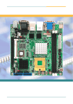
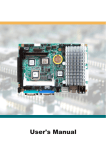
GF Rhodeus Low Power AMD Geode™ LX800 PC/104 CPU Module with CRT/LCD, LAN and CF User’s Manual Copyright 2008 Diamond Systems Corporation 1255 Terra Bella Ave. Mountain View, CA 94043 Tel (650) 810-2500 www.diamondsystems.com Index Table of Contents Chapter 1 - Introduction ....................................................1 1.1 Copyright Notice .............................................................2 1.2 About User’s Manual .....................................................2 1.3 Warning .............................................................................2 1.4 Replacing the lithium battery ......................................3 1.5 Technical Support ..........................................................3 1.6 Warranty............................................................................4 1.7 Packing List .....................................................................5 1.8 Ordering Information .....................................................5 6SHFL¿FDWLRQ ....................................................................6 1.10 Board Dimensions........................................................7 Chapter 2 - Installation ......................................................9 2.1 Block Diagrams ............................................................ 10 2.2 Jumpers and Connectors ........................................... 11 KBM1: Keyboard & Mouse Connector ..................13 LAN1: Fast Ethernet Connector.............................13 IDE1: 44 pin IDE Connector....................................14 PWR1: Power Supply Connector...........................14 PC/104: PC/104 ISA Interface .................................15 JRS1: COM 2 RS-232/422/485 Select.....................16 LLED1: LAN LED Indicators...................................16 JFRT1: Switches and Indicators............................16 IR1: Intrared Connector ..........................................17 VGA1: CRT Connector............................................17 USB1: USB Connector............................................17 FDD1: 20 pins FDD Connector...............................18 JBAT1: CMOS Setup ...............................................18 LPT1: 20 pins Parallel Port Connector..................19 CON1: RS-422/ 485 Output Connector ..................19 LCD1: TTL LCD Connector.....................................20 -i- Index COM1/ COM2: Serial Port Connector ....................20 CFD1: CompactFlash II Socket ..............................21 2.3 The Installation Paths of CD Driver ......................... 22 Chapter 3 - BIOS ................................................................23 3.1 BIOS Introduction ........................................................ 24 3.2 BIOS Setup .................................................................... 24 3.3 Standard CMOS Features .......................................... 25 3.4 Advanced BIOS Features........................................... 28 3.5 Advanced Chipset Features ...................................... 30 3.6 Integrated Peripherals ................................................ 32 3133&,&RQ¿JXUDWLRQV ............................................. 39 3.8 PC Health Status .......................................................... 41 3.9 Load Optimized Defaults .......................................... 42 3.10 Set Password ............................................................ 43 3.11 Save & Exit Setup ...................................................... 44 3.12 Exit Without Saving .................................................. 45 3.13 BIOS Beep Sound code list..................................... 46 3.14 BIOS memory mapping ............................................ 46 3.15 Award BIOS POST Codes ........................................ 47 Chapter 4 - Appendix .......................................................51 4.1 I/O Port Address Map.................................................. 52 4.2 Interrupt Request Lines (IRQ)................................... 53 4.3 DMA Map........................................................................ 53 4.4 Memory Address Map ................................................. 54 4.5 LCD Data Cable Pin Assignment Example........... 55 - ii - Introduction 1 Chapter 1 Introduction Chapter 1 - Introduction -1- Introduction 1.1 Copyright Notice All Rights Reserved. The information in this document is subject to change without prior notice in order to improve the reliability, design and function. It does not represent a commitment on the part of the manufacturer. Under no circumstances will the manufacturer be liable for any direct, indirect, special, incidental, or consequential damages arising from the use or inability to use the product or documentation, even if advised of the possibility of such damages. This document contains proprietary information protected by copyright. All rights are reserved. No part of this manual may be reproduced by any mechanical, electronic, or other means in any form without prior written permission of the manufacturer. 1.2 About User’s Manual This User’s Manual is intended for experienced users and integrators with hardware knowledge of personal computers. If you are not sure about any description in this User’s Manual, please consult your vendor before further handling. 1.3 Warning Single Board Computers and their components contain very delicate Integrated Circuits (IC). To protect the Single Board Computer and its components against damage from static electricity, you should always follow the following precautions when handling it : 1. Disconnect your Single Board Computer from the power source when you want to work on the inside. 2. Hold the board by the edges and try not to touch the IC chips, leads or circuitry. 3. Use a grounded wrist strap when handling computer components. 4. Place components on a grounded antistatic pad or on the bag that came with the Single Board Computer, whenever components are separated from the system. -2- Introduction 1.4 Replacing the lithium battery Incorrect replacement of the lithium battery may lead to a risk of explosion. The lithium battery must be replaced with an identical battery or a battery type recommended by the manufacturer. Do not throw lithium batteries into the trashcan. It must be disposed of in accordance with local regulations concerning special waste. 1.5 Technical Support Please do not hesitate to e-mail our support team when you need assistance www.diamondsystems.com support@diamondsystems.com -3- Introduction 1.6 Warranty This product is warranted to be in good working order for a period of two years from the date of purchase. Should this product fail to be in good working order at any time during this period, we will, at our option, replace or repair it at no additional charge except as set forth in the following terms. 7KLVZDUUDQW\GRHVQRWDSSO\WRSURGXFWVGDPDJHGE\PLVXVHPRGL¿FDWLRQV accident or disaster. 9HQGRUDVVXPHVQROLDELOLW\IRUDQ\GDPDJHVORVWSUR¿WVORVWVDYLQJVRUDQ\ other incidental or consequential damage resulting from the use, misuse of, or inability to use this product. Vendor will not be liable for any claim made by any other related party. Vendors disclaim all other warranties, either expressed or implied, including EXWQRWOLPLWHGWRLPSOLHGZDUUDQWLHVRIPHUFKDQWLELOLW\DQG¿WQHVVIRU a particular purpose, with respect to the hardware, the accompanying product’s manual(s) and written materials, and any accompanying hardware. 7KLVOLPLWHGZDUUDQW\JLYHV\RXVSHFL¿FOHJDOULJKWV Return authorization must be obtained from the vendor before returned merchandise will be accepted. Authorization can be obtained by calling or faxing the vendor and requesting a Return Merchandise Authorization (RMA) number. Returned goods should always be accompanied by a clear problem description. -4- Introduction 1.7 Packing List 1 x Rhodeus Single Board Computer 1 x CD-ROM 1 x Quick Installation Guide If any of the above items is damaged or missing, contact your vendor immediately. 1.8 Ordering Information Rhodeus Cable Kit (Optional) PC/104 CPU module with AMD Geode™ LX800 (500MHz), 1 x SO-DIMM, CRT/LCD & LAN 1 x USB Cable 2 x COM Port Cable 1 x FDD Flat Cable 1 x IDE Cable 1 x Parallel Port Cable 1 x LAN Cable 1 x VGA Cable 1 x KB/MS Cable -5- Introduction 6SHFL¿FDWLRQ Form Factor PC/104 CPU module Processor AMD Geode™ LX800 Cache 64K L1 cache and 128K L2 cache Chipset AMD LX800 + CS5536 System Memory 1 x 200 pins DDR SO-DIMM up to 1GB SDRAM VGA/ LCD Controller AMD Geode LX series CPU integrated VGA controller with 2D Engine (Shared memory Max. 64MB) Ethernet Realtek 8100CL 10/100 base-T Ethernet LCD Supports 18/24-bit TTL up to 1280 x 1024 I/O Chips W83627HG BIOS Phoenix-Award BIOS IDE Interface 1 x Ultra DMA 33, support 2 IDE devices Serial Port 2 x RS-232 ports COM2: RS-232/RS-422/RS-485 selectable Parallel Port / Floppy 1 x SPP/EPP/ECP mode 1 x Floppy connector KBMS Standard PS/2 Keyboard and Mouse Universal Serial Bus 2 x USB 2.0 ports PCI to ISA bridge ITE8888G Expansion Bus 1 x PC/104 interface Flash Disk 1 x Type II Compact Flash Disk Socket up to 8GB Hardware Monitor Integrated in W83627HG RTC AMD Geode CS5536 built-in RTC with lithium battery Power Input Connector 1*4 pins power connector Operation Temp. -20oC to +70oC or -40oC to +85oC Watchdog Timer 1 - 255 Level (Sec. or Min.) Dimension (L x W) 96 x 90 mm (3.8” x 3.5”) -6- Introduction 1.10 Board Dimensions Unit:mm -7- Introduction Unit:mm -8- Installation 2 Chapter 2 Installation Chapter 2 - Installation -9- Installation 2.1 Block Diagrams VGA LCD Analog R.G.B. TTL 18/24 bit AMD Geode LX800 CPU 500MHz 1 x 200pin SO-DIMM Socket Memory Bus PCI to ISA Bridge PCI Bus ISA Bus PCI LAN Controller 4 x USB 1 x IDE PC/104 LAN RJ-45 USB I/F IDE ATA I/F AMD Geode CS5536 LPC I/F Super IO Controller 1 x CF COM1 LPT1 KB COM2 FDD MS IrDA - 10 - Installation 2.2 Jumpers and Connectors 15 CON1 1 LCD1 16 COM2 1 39 2 40 18 COM1 17 9 1 9 1 10 2 10 2 KBM1 1 1 1 2 LAN1 2 1 LPT1 9 44 2 43 14 IDE1 3 19 1 FDD1 20 2 12 1 JBAT1 19 20 1 USB1 13 2 1 2 1 11 9 PC/104 5 PWR1 4 4 B1 A1 B32 A32 1 C0 D0 15 16 C19 6 5 D19 1 2 1 1 VGA1 IR1 JFRT1 LLED1 10 9 8 7 - 11 - 21 JRS1 6 Installation Jumper / Connector Quick Reference Jumpers Label Function JRS1 COM2 RS-232/422/485 Select JBAT1 CMOS Jumper Settings Connectors DIMM1 200 pins DDR SDRAM DIMM Socket PC104_1 PC/104 for ISA Interface KBM1 PS/2 Keyboard and Mouse VGA1 CRT Display LCD1 TTL LCD Panel Connector COM1 ~ COM2 Serial Ports CON1 RS-422/485 Output IR1 Infrared (IR) Connector LPT1 Parallel Port LAN1 LAN Ethernet Connector LLED1 LAN LED Connector USB1 USB 1/2 Connector PWR1 Power Connector Small 4P JFRT1 Front Panel (Switches and Indicators) FDD1 Floppy Disk Drive Connector IDE1 Primary IDE Connector CFD1 Compact Flash Socket - 12 - Installation KBM1: Keyboard & Mouse Connector (1) Connector type: 2.0mm pitch 1x6 pins wafer connector Pin Description 1 KB_DATA 2 GND 3 MS_DATA 4 KB_CLK 5 KB_VCC 6 MS_CLK 1 LAN1: Fast Ethernet Connector (2) Pin Description Pin Description 1 TX+ 2 TX- 3 RX+ 4 N/C 5 N/C 6 RX- 7 N/C 8 N/C 9 GND 10 N/C (Key) Connector type: 2.0mm pitch 2x5 pin header - 13 - 1 2 9 10 Installation IDE1: 44 pins IDE Connector (3) Connector type: 2.0mm pitch 2x22 pin header Pin Description Pin Description 1 IDE RESET 2 GND 3 DATA7 4 DATA8 5 DATA6 6 DATA9 7 DATA5 8 DATA10 9 DATA4 10 DATA11 11 DATA3 12 DATA12 13 DATA2 14 DATA13 15 DATA1 16 DATA14 17 DATA0 18 DATA15 19 GND 20 N/C (Key) 21 REQ 22 GND 23 IO WRITE 24 GND 25 IO READ 26 GND 27 IO READY 28 IDESEL 29 DACK 30 GND 31 IRQ14 32 N/C 33 ADDR1 34 DIAG 35 ADDR0 36 ADDR2 37 CS#2 38 CS#3 39 IDEACTP 40 GND 41 +5V 42 +5V 43 GND 44 N/C 1 2 3 4 4 PWR1: Power Supply Connector (4) Pin Description 1 +5V 2 GND 3 GND 4 +12V 1 Connector type: 2.54mm pitch 1x4 pins wafer one wall connector - 14 - Installation PC/104: PC/104 ISA Interface (5) 1 B 2 3 B 2 3 A 1 A Pin D0 D1 D2 D3 D4 D5 D6 D7 D8 D9 D10 D11 D12 D13 D14 D15 D16 D17 D18 D19 Description GND MEMCS16# IOCS16# IRQ10 IRQ11 IRQ12 IRQ15 IRQ14 DACK0# DREQ0 DACK5# DREQ5 DACK6# DREQ6 DACK7# DREQ7 +5V MASTER# GND GND 0 C 19 C 0 D 19 D Pin C0 C1 C2 C3 C4 C5 C6 C7 C8 C9 C10 C11 C12 C13 C14 C15 C16 C17 C18 C19 Description GND SBHE# LA23 LA22 LA21 LA20 SA19 SA18 SA17 MEMR# MEMW# SD8 SD9 SD10 SD11 SD12 SD13 SD14 SD15 GND Pin A1 A2 A3 A4 A5 A6 A7 A8 A9 A10 A11 A12 A13 A14 A15 A16 A17 A18 A19 A20 A21 A22 A23 A24 A25 A26 A27 A28 A29 A30 A31 A32 Description IOCHCK# SD7 SD6 SD5 SD4 SD3 SD2 SD1 SD0 IOCHRDY AEN SA19 SA18 SA17 SA16 SA15 SA14 SA13 SA12 SA11 SA10 SA9 SA8 SA7 SA6 SA5 SA4 SA3 SA2 SA1 SA0 GND Connector type: PC104 PRESS FIT 2x20P connector - 15 - Pin B1 B2 B3 B4 B5 B6 B7 B8 B9 B10 B11 B12 B13 B14 B15 B16 B17 B18 B19 B20 B21 B22 B23 B24 B25 B26 B27 B28 B29 B30 B31 B32 Description GND RST_DRV +5V IRQ9 N/C DREQ2 N/C 0WS# +12V GND SMEMW# SMEMR# IOW# IOR# DACK3# DREQ3 DACK1# DREQ1 REFRESH# SYSCLK IRQ7 IRQ6 IRQ5 IRQ4 IRQ3 DACK2# TC BALE +5V ISA_CLK GND GND Installation JRS1: COM 2 RS-232/422/485 Select (6) ,WFDQEHFRQ¿JXUHG&20WRRSHUDWHLQ5656RU56PRGH Connector type: 2.00mm pitch 2x3 pin header. Select 1-2 3-4 5-6 RS-232 (Default) ON OFF OFF RS-422 OFF ON OFF RS-485 OFF OFF ON 1 2 1 2 1 2 5 6 5 6 5 6 LLED1: LAN LED indicators (7) Connector type: 2.54mm pitch 1x4 pin header. Pin Description 1 LAN1_ACTIVE- 2 LAN1_ACTIVE+ 3 LAN1_LINK- 4 LAN1_LINK+ 1 JFRT1: Switches and Indicators (8) It provides connectors for system indicators that provides light indication of the computer activities and switches to change the computer status. Connector type: 2.54mm pitch 1x8 pin header. Pin Description 1 1 RESET+ 2 RESET- 3 PWRLED+ 4 PWRLED- 5 HDD LED+ 6 HDD LED- 7 SPK OUT+ 8 SPK OUT- - 16 - Installation IR1: Infrared Connector (9) Connector Type: 2.54mm pitch 5 pins header Pin Voltage 1 +5V 2 N/C 3 IRRX 4 GND 5 IRTX 1 VGA1: CRT Connector (10) Connector type: 2.0mm pitch 2x5 pin header Pin Description Pin Description 1 RED 2 GREEN 3 BLUE 4 N/C 5 GND 6 GND 7 GND 8 GND 9 N/C 10 GND 11 N/C (Key) 12 VDDAT 13 HSYNC 14 VSYNC 15 VDCLK 16 N/C 1 2 15 16 USB1: USB Connector (11) USB1 supports two USB 2.0 w/ 480MB/s by pin header Pin Description Pin Description 1 +5V 2 +5V 3 USBD- 4 USBD- 5 USBD+ 6 USBD+ 7 GND 8 GND 9 GND 10 N/C (Key) Connector type: 2.0mm pitch 2x5 pin header - 17 - 1 2 9 10 Installation FDD1: 20 pins FDD Connector (12) Connector type: 2.0mm pitch 2x10 pin header Pin Description Pin Description 1 GND 2 Drive density Select 0 3 GND 4 N/C (Key) 5 GND 6 Drive Density Select 1 7 Write Data# 8 Index# 9 Write Gate# 10 Motor Enable A# 11 Track 0# 12 Driver Select B# 13 Write Protect# 14 Driver Select A# 15 Read Data# 16 Motor Enable B# 17 Head Select# 18 Direction# 19 Disk Change# 20 Step# 1 2 19 2 0 JBAT1: CMOS Setup (13) Connector type: 2.0 mm pitch 1x3 pin header. Pin Mode 1-2 Keep CMOS (Default) 1 2 3 2-3 Clear CMOS 1 2 3 Note: After Clear CMOS, please make sure to load default in BIOS immediately. - 18 - Installation LPT1: 20 pins Parallel Port Connector (14) Connector type: 2.0mm pitch 2x10 pin header Pin Description Pin Description 1 STROBE 2 AFD 3 PTD0 4 ERROR 5 PTD1 6 INIT 7 PTD2 8 SLIN 9 PTD3 10 GND 11 PTD4 12 GND 13 PTD5 14 GND (Key) 15 PTD6 16 BUSY 17 PTD7 18 PE 19 ACK 20 SELECT 1 19 CON1: RS-422/ 485 Output Connector (15) Connector type: 2.0mm pitch 1x4 pins wafer connector RS-422 RS-485 1 TX+ Data+ 2 TX- Data- 3 RX+ N/C 4 RX- N/C 1 Pin - 19 - 1 2 0 2 Installation LCD1: TTL LCD Connector (16) Connector type: DF-13-40DP-1.25V Pin Description Pin Description 2 5V_SAFE 1 5V_SAFE 4 GND 3 GND 6 3V_SAFE 5 3V_SAFE 8 GND 7 N/C 10 PD1 9 PD0 12 PD3 11 PD2 14 PD5 13 PD4 16 PD7 15 PD6 18 PD9 17 PD8 20 PD11 19 PD10 22 PD13 21 PD12 24 PD15 23 PD14 26 PD17 25 PD16 28 PD19 27 PD18 30 PD21 29 PD20 32 PD23 31 PD22 34 GND 33 GND 36 VS 35 SHIFT CLOCK 38 HS 37 DE 40 ENAVDD 39 ENABLK COM1/ COM2: Serial Port Connector (17), (18) Pin Description Pin Description 1 DCD 2 RXD 3 TXD 4 DTR 5 GND 6 DSR 7 RTS 8 CTS 9 RI 10 N/C Connector type: 2.0mm pitch 2x5 box pin header - 20 - 1 2 9 10 Installation CFD1: CompactFlash II Socket CFD1 does not support hot swap. 'HIDXOWHGE\¿UVW,'(6ODYH Pin Description Pin Description 1 PDD3 26 GND 2 PDD4 27 PDD11 3 PDD5 28 PDD12 4 PDD6 29 PDD13 5 PDD7 30 PDD14 6 CS#0 31 PDD15 7 GND 32 CS#1 1 6 2 5 2 0 5 8 GND 33 GND 9 GND 34 PDIOR# 10 GND 35 PDIOW# 11 GND 36 +5V 12 GND 37 IRQ14 13 +5V 38 +5V 14 GND 39 CSEL# 15 GND 40 N/C 16 GND 41 IDE_RST# 17 GND 42 PDRDY 18 PDA2 43 PDREQ 19 PDA1 44 PDACK# 20 PDA0 45 IDE_ACT# 21 PDD0 46 CFDIAG 22 PDD1 47 PDD8 23 PDD2 48 PDD9 24 CF_ICS16# 49 PDD10 25 GND 50 GND - 21 - Installation 2.3 The Installation Paths of CD Driver Driver Path CHIPSET \Chiset\AMD\LX ISA \ISA\ITE8888 LAN \Ethernet\REALTEK\8100C VGA \Graphics\AMD\LX - 22 - BIOS 3 Chapter 3 BIOS Chapter 3 - BIOS - 23 - BIOS 3.1 BIOS Introduction The Award BIOS (Basic Input/Output System) installed in your computer system’s. The BIOS provides for a standard device such as disk drives, serial ports and parallel ports. It also adds password protection as well as special VXSSRUWIRUGHWDLOHG¿QHWXQLQJRIWKHFKLSVHWFRQWUROOLQJWKHHQWLUHV\VWHP 3.2 BIOS Setup The Award BIOS provides a Setup utility program for specifying the system FRQ¿JXUDWLRQVDQGVHWWLQJV7KH%,26520RIWKHV\VWHPVWRUHVWKH6HWXS utility. When you turn on the computer, the Award BIOS is immediately activated. Pressing the <Del> key immediately allows you to enter the Setup utility. If you a little bit late press the <Del> key, POST (Power On Self Test) will continue with its test routines, thus preventing you from invoking the Setup. If you still wish to enter Setup, restart the system by pressing the ”Reset” button or simultaneously pressing the <Ctrl>, <Alt> and <Delete> keys. You can also restart by turning the system Off and back On again. The following message will appear on the screen: Press <DEL> to Enter Setup In general, you press the arrow keys to highlight items, <Enter> to select, the <PgUp> and <PgDn> keys to change entries, <F1> for help and <Esc> to quit. When you enter the Setup utility, the Main Menu screen will appear on the screen. The Main Menu allows you to select from various setup functions and exit choices. - 24 - BIOS 3.3 Standard CMOS Features “Standard CMOS Features” allows you to record some basic hardware FRQ¿JXUDWLRQVLQ\RXUFRPSXWHUV\VWHPDQGVHWWKHV\VWHPFORFNDQG error handling. If the CPU card is already installed in a working system, you will not need to select this option. You will need to run the Standard CMOS option, however, if you change \RXUV\VWHPKDUGZDUHFRQ¿JXUDWLRQVVXFKDVRQERDUGEDWWHU\IDLOVRUWKH FRQ¿JXUDWLRQVWRUHGLQWKH&026PHPRU\ZDVORVWRUGDPDJHG Date The date format is: Day : Sun to Sat Month : 1 to 12 Date : 1 to 31 Year : 1999 to 2099 Time Hour : 00 to 23 Minute : 00 to 59 Second : 00 to 59 To set the date & time, highlight the “Date” & “Time” and use the <PgUp>/ <PgDn> or +/- keys to set the current time. The time format is: - 25 - BIOS IDE Primary HDDs / IDE Secondary HDDs The onboard PCI IDE connectors provide Primary and Secondary channels for connecting up to four IDE hard disks or other IDE devices. (DFKFKDQQHOFDQVXSSRUWXSWRWZRKDUGGLVNVWKH¿UVWLVWKH³0DVWHU´DQG the second is the “Slave”. 3UHVV(QWHU!WRFRQ¿JXUHWKHKDUGGLVN7KHVHOHFWLRQVLQFOXGH$XWR 0DQXDODQG1RQH6HOHFWµ0DQXDO¶WRGH¿QHWKHGULYHLQIRUPDWLRQPDQXDOO\ You will be asked to enter the following items. Cylinder: Number of cylinders Head: Number of read/write heads Precomp: Write precompensation Landing Zone: Landing zone Sector: Number of sectors The Access Mode selections are as follows: CHS (HD < 528MB) LBA (HD > 528MB and supports Logical Block Addressing) Large (for MS-DOS only) Auto Drive A / Drive B 7KHVH¿HOGVLGHQWLI\WKHW\SHVRIÀRSS\GLVNGULYH$RUGULYH%WKDWKDV EHHQLQVWDOOHGLQWKHFRPSXWHU7KHDYDLODEOHVSHFL¿FDWLRQVDUH 1.2M, 5.25 in. None 360K, 5.25 in. 720K, 3.5 in. 1.44M, 3.5 in. 2.88M, 3.5 in. Video 7KLV¿HOGVHOHFWVWKHW\SHRIYLGHRGLVSOD\FDUGLQVWDOOHGLQ\RXUV\VWHP You can choose the following video display cards: EGA/VGA For EGA, VGA, SEGA, SVGA or PGA monitor adapters. (default) CGA 40 Power up in 40 column mode. CGA 80 Power up in 80 column mode. MONO For Hercules or MDA adapters. - 26 - BIOS Halt On 7KLV¿HOGGHWHUPLQHVZKHWKHURUQRWWKHV\VWHPZLOOKDOWLIDQHUURULV detected during power up. All errors (default) Whenever the BIOS detects a non-fatal error, the system will stop and you will be prompted. The system boot will not be halted for any error that No errors may be detected. All, But Keyboard The system boot will not be halted for a keyboard error; it will stop for all other errors. All, But Diskette The system boot will not be halted for a disk error; it will stop for all other errors. All, But Disk/Key The system boot will not be halted for a keyboard or disk error; it will stop for all others. - 27 - BIOS 3.4 Advanced BIOS Features Quick Power On Self Test :KHQHQDEOHGWKLV¿HOGVSHHGVXSWKH3RZHU2Q6HOI7HVW3267DIWHU the system is turned on. If it is set to Enabled, BIOS will skip some items. Setting: Enabled (Default), Disabled. First/ Second Boot Device 7KHVH¿HOGVGHWHUPLQHWKHGULYHWKDWWKHV\VWHPVHDUFKHV¿UVWIRUDQ operating system. The options available include Setting: Floppy, LS120, HDD-0, SCSI, CDROM, HDD-1, ZIP100, USB-FDD, USB-ZIP, USB-CDROM, USB-HDD, LAN and Disabled. Boot Other Device It allows the system to search for an OS from other devices other than the ones selected in the First/ Second/ Third Boot Device. Setting: Enabled (Default), Disabled. - 28 - BIOS Boot Up NumLock Status It allows you to activate the NumLock function after you power up the system. Setting: On (Default), Off. Security Option It allows you to limit access to the System and Setup. When you select System, the system prompts for the User Password every time you boot up. When you select Setup, the system always boots up and prompts for the Supervisor Password only when the Setup utility is called up. Setting: Setup (Default), System. Cyrix 6x86/MII CPUID Disable CPU ID instruction if you are using Netware v5.0. Setting: Enabled (Default), Disabled. - 29 - BIOS 3.5 Advanced Chipset Features CAS Latency Time It allows CAS latency time in HCLKs as 2 or 2.5. The system board designer VKRXOGVHWWKHYDOXHVLQWKLV¿HOGGHSHQGLQJRQWKH'5$0LQVWDOOHG'R QRWFKDQJHWKHYDOXHVLQWKLV¿HOGXQOHVV\RXFKDQJHVSHFL¿FDWLRQVRIWKH installed DRAM or CPU. Setting: 2.5 (Default), 2. Interleave Select It allows you to Use the Interleave Select option to specify how the cache memory is interleaved. Setting: LOI (Default), HOI. XOR BA0 Setting: Disabled (Default), Enabled. XOR BA1 Setting: Disabled (Default), Enabled. - 30 - BIOS XOR MB0 Setting: Disabled (Default), Enabled. XOR Bit Select Setting: 18 (Default), 19, 20, 21. Video Memory Size In order to determine how much memory is allocated to the video graphics device. Setting: None, 8M (Default), 16M, 32M, 64M, 128M, 254M. Output display In order to specify the display devices the system is connected to. Setting: Flat Panel, CRT (Default), Panel & CRT. )ODW3DQHO&RQ¿JXUDWLRQ ,WDOORZV\RXWRRSHQWKH)ODW3DQHO&RQ¿JXUDWLRQPHQX Memory Hole At 15M-16M In order to improve performance, certain space in memory can be reserved for ISA cards. This memory must be mapped into the memory space below 16 MB. Setting: Disabled (Default), Enabled. - 31 - BIOS 3.6 Integrated Peripherals OnChip IDE Devicev >>> On-Chip IDE Channel 1 The integrated peripheral controller contains an IDE interface with support for two IDE channels. Select Enabled to activate each channel separately. Setting: Disabled, Enabled (Default). - 32 - BIOS IDE Primary Master/Slave PIO It allows your system HDD controller to run faster. Rather than having the BIOS issue with a series of commands that transferring to or from the disk drive, PIO (Programmed Input/Output) allows the BIOS to communicate with the controller and CPU directly. When Auto is selected, the BIOS will select the best available mode. Setting: Auto (Default), Mode 0, Mode 1, Mode 2, Mode 3, Mode 4. IDE Primary Master/Slave UDMA It allows your system to improve disk I/O throughput to 33MB/sec with the Ultra DMA33 feature. Setting: Disabled, Auto. IDE DMA Transfer Access Setting: Disabled, Enabled (Default). IDE HDD Block Mode It allows your HDD controller to use the fast block mode to transfer data to and from your HDD drive. Setting: Disabled, Enabled (Default). - 33 - BIOS SuperIO Device >>> Onboard FDC Controller Select “Enabled” if you wish to use it. Select “Disabled” if you don’t wish to use it. Setting: Disabled, Enabled (Default). Serial/ Onboard Parallel Port It allows you to select the onboard serial and parallel ports with their addresses. Setting: Serial Port 1 3F8/IRQ4 (Default) 2F8/IRQ3 (Default) Serial Port 2 Parallel Port 378H/IRQ7 (Default) UART Mode Select It determines the UART 2 mode in your computer. Setting: IrDA, ASKIR, Normal (Default). RxD, TxD Active Setting: Hi,Hi , Hi,Lo (Default) , Lo,Hi , Lo,Lo. IR Transmission Delay Setting: Disabled, Enabled (Default). - 34 - BIOS UR2 Duplex Mode Setting: Full, Half (Default). Use IR Pins Setting: RxD2,TxD2 , IR-Rx2Tx2 (Default). Parallel Port Mode Setting: SPP (Default) EPP ECP ECP+EPP Normal EPP Mode Select Setting: EPP1.9, EPP1.7 (Default) ECP Mode Use DMA Setting: 1, 3 (Default). - 35 - BIOS IT8888 ISA Decode IO >>> It allows you to use the IT8888 ISA Decode IO menu to set the IO memory range for the onboard ISA. Decode I/O Space 0/ 1/ 2/ 3/ 4/ 5 It allows you to allocate system resources to the ISA bridge and to enable the function correctly. Setting: Disabled, Enabled (Default). Decode I/O Speed 0/ 1/ 2/ 3/ 4/ 5 It allows you to specify the speed of the ISA bus. Setting: Subtractive Speed, Slow Speed, Medium Speed, Fast Speed. - 36 - BIOS Decode I/O Address 0/ 1/ 2/ 3/ 4/ 5 [15:4] It allows you to allocate an address to the ISA bus. The address may range from 0001 to 0FFF. Decode I/O Size 0/ 1/ 2/ 3/ 4/ 5 It allows you to specify the size of the ISA bus. Setting: 1 Byte, 2 Bytes, 4 Bytes, 8 Bytes, 16 Bytes, 32 Bytes, 64 Bytes, 128 Bytes. IT8888 ISA Decode Memory >>> It allows you to use the IT8888 ISA Decode Memory to set the resources for the onboard ISA bus. Decode Memory Space 0/ 1/ 2/ 3 It allows you to allocate memory resources to the ISA bridge and to enable the function correctly. Setting: Disabled (Default), Enabled. - 37 - BIOS Decode Memory Speed 0/ 1/ 2/ 3 It allows you to specify the memory speed of the ISA bus. Setting: Subtractive Speed, Slow Speed, Medium Speed, Fast Speed. Decode Memory Addr. 0/ 1/ 2/ 3 [23: It allows you to allocate a memory address to the ISA bus. The address may range from 0001 to 0FFF. Decode Memory Size 0/ 1/ 2/ 3 It allows you to specify the memory size of the ISA bus. Setting: 16 KB, 32 KB, 64 KB, 128 KB, 256 KB, 512 KB, 1MB, 2MB. IT8888 DDMA >>> Suppose that the ISA bus card is required DMA1 & DMA5. Set “DDMA1 Support” & “DDMA5 Support” to “Enabled”. Onboard Lan Boot ROM Setting: Enabled, Disabled (Default). - 38 - BIOS 3133&,&RQ¿JXUDWLRQV PNP OS Installed It allows you to enable the PNP OS Install option if it is supported by the OS installed. Setting: No (Default), Yes. 5HVHW&RQ¿JXUDWLRQ'DWD ,WDOORZV\RXWRGHWHUPLQHZKHWKHUWRUHVHWWKHFRQ¿JXUDWLRQGDWDRUQRW Setting: Disabled (Default), Enabled. Resources Controlled By 7KLV3Q3%,26FDQFRQ¿JXUHDOORIWKHERRWDQGFRPSDWLEOHGHYLFHVZLWKWKH use of a PnP operating system. Setting: Auto(ESCD) (Default), Manual. - 39 - BIOS IRQ Resources ,WDOORZV\RXWRFRQ¿JXUHWKH,54'0$5HVRXUFHV Memory Resources ,WDOORZV\RXWRFRQ¿JXUHWKH0HPRU\5HVRXUFHV PCI/VGA Palette Snoop Some non-standard VGA display cards may not show colors properly. It allows you to set whether or not MPEG ISA/VESA VGA cards can display with PCI/VGA. When “Enabled”, a PCI/VGA can display with an MPEG ISA/VESA VGA card. When “Disabled”, a PCI/VGA can not display with an MPEG ISA/VESA VGA card. Setting: Disabled (Default), Enabled. - 40 - BIOS 3.8 PC Health Status Current CPU Temperature CPU/ MEM VCore VCC3/ +5V/ +12V/ VBAT(V)/ 5VSB - 41 - BIOS 3.9 Load Optimized Defaults ,WDOORZV\RXWRORDGWKHGHIDXOWYDOXHVWR\RXUV\VWHPFRQ¿JXUDWLRQ7KH default setting is optimal and enabled all high performance features. - 42 - BIOS 3.10 Set Password Using Password to set a password that will be used exclusively on the system. To specify a password, highlight the type you want and press <Enter>. The Enter Password: message prompts on the screen. Type the password, XSWRHLJKWFKDUDFWHUVLQOHQJWKDQGSUHVV(QWHU!$QGWKHV\VWHPFRQ¿UPV your password by asking you to type it again. After setting a password, the screen automatically returns to the main screen. To disable a password, just press the <Enter> key when you are prompted WRHQWHUWKHSDVVZRUG$PHVVDJHZLOOFRQ¿UPWKHSDVVZRUGWREHGLVDEOHG Once the password is disabled, the system will boot, then you can enter BIOS Setup freely. - 43 - BIOS 3.11 Save & Exit Setup Typing “Y”, you will quit the setup utility and save all the changes into the CMOS memory. Typing “N”, you will return to Setup utility. - 44 - BIOS 3.12 Exit Without Saving 7\SLQJ³<´ZLOOTXLWWKH6HWXSXWLOLW\ZLWKRXWVDYLQJWKHPRGL¿FDWLRQV Typing “N” will return you to Setup utility. - 45 - BIOS 3.13 BIOS Beep Sound code list Beep Sound Message 1 short (Beep) System booting is normally 2 short (Beep) CMOS setting error 1 long - 1 short (Beep) DRAM error 1 long - 2 short (Beep) Display card or monitor connected error 1 long - 3 short (Beep) Keyboard error 1 long - 9 short (Beep) ROM error Long (Beep) continuous DRAM hasn’t inset correctly Short (Beep) continuous POWER supply has problem 3.14 BIOS memory mapping Address Device Description E000:0000h - F000:FFFFh System BIOS Area D000:2000h - D000:FFFFh Free space D000:0000h - D000:1FFFh LAN ROM C000:E000h - CF00:FFFFh Free space C000:0000h - C000:DFFFh VGA BIOS A000:0000h - B000:FFFFh VGA RAM 0000:0000h - 9000:FFFFh DOS 640K - 46 - BIOS 3.15 Award BIOS POST Codes CFh Test CMOS read/write functionality chipset initialization: Disable shadow RAM, L2 cache (socket 7 C0h Early and below), program basic chipset registers memory: Auto detection of DRAM size, type and ECC, auto C1h Detect detection of L2 cache (socket 7 and below) C3h Expand compressed BIOS code to DRAM C5h Call chipset hook to copy BIOS back to E000 & F000 shadow RAM 01h Expand the Xgroup codes located in physical memory address 1000:0 02h Reserved 03h Initial Superio_Early_Init switch 04h Reserved 05h %ODQNRXWVFUHHQ&OHDU&026HUURUÀDJ 06h Reserved 07h Clear 8042 interface; Initialize 8042 self test Test special keyboard controller for Winbond 977 series Super I/O 08h chips; Enable keyboard interface 09h Reserved Disable PS/2 mouse interface (optional); Auto detect ports for 0Ah keyboard & mouse followed by a port & interface swap (optional); Reset keyboard for Winbond 977 series Super I/O chips 0Bh Reserved 0Ch Reserved 0Dh Reserved F000h segment shadow to see whether it is read/write capable or 0Eh Test not. If test fails, keep beeping the speaker 0Fh Reserved 10h $XWRGHWHFWÀDVKW\SHWRORDGDSSURSULDWHÀDVKUHDGZULWHFRGHVLQWR the run time area in F000 for ESCD & DMI support 11h Reserved walking 1’s algorithm to check out interface in CMOS circuitry. 12h Use Also set real time clock power status and then check for override 13h Reserved chipset default values into chipset. Chipset default values 14h Program are MODBINable by OEM customers 15h Reserved 16h Initial Early_Init_Onboard_Generator switch 17h Reserved CPU information including brand, SMI type (Cyrix or Intel) and 18h Detect CPU level (586 or 686) 19h Reserved 1Ah Reserved Initial interrupts vector table. ,IQRVSHFLDOVSHFL¿HGDOO+: 1Bh interrupts are directed to SPURIOUS_INT_HDLR & S/W interrupts to SPURIOUS_soft_HDLR 1Ch Reserved 1Dh Initial EARLY_PM_INIT switch 1Eh Reserved 1Fh Load keyboard matrix (notebook platform) - 47 - BIOS 20h 21h 22h 23h 24h 25h 26h 27h 28h 29h 2Ah 2Bh 2Ch 2Dh 2Eh 2Fh 30h 31h 32h 33h 34h 35h 36h 37h 38h 39h 3Ah 3Bh 3Ch 3Dh 3Eh 3Fh 40h 41h 42h 43h 44h 45h 46h Reserved HPM initialization (notebook platform) Reserved Check validity of RTC value; Load CMOS settings into BIOS stack. If CMOS checksum fails, use default value instead; Prepare BIOS resource map for PCI & PnP use. If ESCD is valid, take into consideration of the ESCD's legacy information; Onboard clock generator initialization. Disable respective clock resource to empty PCI & DIMM slots; Early PCI initialization - Enumerate PCI bus number, assign memory & I/O resource, search for a valid VGA device & VGA BIOS, and put it into C000:0 Reserved Reserved Reserved Initialize INT 09 buffer Reserved Program CPU internal MTRR (P6 & PII) for 0-640K memory address; Initialize the APIC for Pentium class CPU; Program early chipset according to CMOS setup; Measure CPU speed; Invoke video BIOS Reserved Reserved Reserved Initialize multilanguage; Put information on screen display, including Award title, CPU type, CPU speed, etc... Reserved Reserved Reserved Reserved Reserved Reset keyboard except Winbond 977 series Super I/O chips Reserved Reserved Reserved Reserved Reserved Reserved Reserved Reserved Test 8254 Reserved Test 8259 interrupt mask bits for channel 1 Reserved Test 9259 interrupt mask bits for channel 2 Reserved Reserved Test 8259 functionality Reserved Reserved Reserved - 48 - BIOS 47h 48h 49h 4Ah 4Bh 4Ch 4Dh 4Eh 4Fh 50h 51h 52h 53h 54h 55h 56h 57h 58h 59h 5Ah 5Bh 5Ch 5Dh 5Eh 5Fh 60h 61h 62h 63h 64h 65h 66h 67h 68h 69h 6Ah 6Bh 6Ch 6Dh 6Eh 6Fh Initialize EISA slot Reserved Calculate total memory by testing the last double last word of each 64K page; Program writes allocation for AMD K5 CPU Reserved Reserved Reserved Reserved Program MTRR of M1 CPU; initialize L2 cache for P6 class CPU & program cacheable range; Initialize the APIC for P6 class CPU; On MP platform, adjust the cacheable range to smaller one in case the cacheable ranges between each CPU are not identical Reserved Initialize USB Reserved Test all memory (clear all extended memory to 0) Reserved Reserved Display number of processors (multi-processor platform) Reserved Display PnP logo; Early ISA PnP initialization and assign CSN to every ISA PnP device Reserved Initialize the combined Trend Anti-Virus code Reserved Show message for entering AWDFLASH.EXE from FDD (optional feature) Reserved Initialize Init_Onboard_Super_IO switch; Initialize Init_Onboard_ AUDIO switch Reserved Reserved Okay to enter Setup utility Reserved Reserved Reserved Reserved Initialize PS/2 mouse Reserved Prepare memory size information for function call: INT 15h ax=E820h Reserved Turn on L2 cache Reserved Program chipset registers according to items described in Setup & $XWR&RQ¿JXUDWLRQWDEOH Reserved Assign resources to all ISA PnP devices; Auto assign ports to onboard COM ports if the corresponding item in Setup is set to “AUTO” Reserved ,QLWLDOL]HÀRSS\FRQWUROOHU6HWXSÀRSS\UHODWHG¿HOGVLQKDUGZDUH - 49 - BIOS 70h 71h 72h 73h 74h 75h 76h 77h 78h 79h 7Ah 7Bh 7Ch 7Dh 7Eh 7Fh 80h 81h 82H 83H 84h 85h 86h 87h 88h 89h 90h 91h 92h 93h 94h 95h 96h FFh Reserved Reserved Reserved (QWHU$:')/$6+(;(LI$:')/$6+(;(LVIRXQGLQÀRSS\GLYH and ALT+F2 is pressed Reserved Detect and install all IDE devices: HDD, LS120, ZIP, CDROM... Reserved Detect serial ports and parallel ports Reserved Reserved Detect and install coprocessor Reserved Reserved Reserved Reserved Switch back to text mode if full screen logo is supported: if errors occur, report errors & wait for keys, if no errors occur or F1 key is pressed continue - Clear EPA or customization logo Reserved Reserved Call chipset power management hook: Recover the text fond used by EPA logo (not for full screen logo), If password is set, ask for password Save all data in stack back to CMOS Initialize ISA PnP boot devices Final USB initialization; NET PC: Build SYSID structure; Switch screen back to text mode; Set up ACPI table at top of memory; Invoke ISA adapter ROM’s; Assign IRQ’s to PCI devices; Initialize APM; Clear noise of IRQ’s Reserved Reserved Reserved Reserved Reserved Reserved Reserved Read HDD boot sector information for Trend Anti-Virus code (QDEOH/FDFKH3URJUDPERRWXSVSHHG&KLSVHW¿QDOLQLWLDOL]DWLRQ 3RZHUPDQDJHPHQW¿QDOLQLWLDOL]DWLRQ&OHDUVFUHHQDQGGLVSOD\ summary table; Program K^ write allocation; Program P6 class write combining Program daylight saving; Update keyboard LED and typematic rate Build MP table; Build and update ESCD; Set CMOS century to 20h or 19h; Load CMOS time into DOS timer tick; Build MSIRQ routing table Boot attempt (INT 19h) - 50 - Appendix 4 Chapter 4 Appendix Chapter 4 - Appendix - 51 - Appendix 4.1 I/O Port Address Map Each peripheral device in the system is assigned a set of I/O port addresses which also becomes the identity of the device. The following table lists the I/O port addresses used. Address Device Description 00000022 - 0000003F PCI bus 00000044 - 00000047 PCI bus 0000004C - 0000006F PCI bus 00000060 - 00000060 PC/AT Enhanced PS/2 Keyboard 00000064 - 00000064 PC/AT Enhanced PS/2 Keyboard 00000072 - 0000007F PCI bus 00000090 - 00000091 PCI bus 00000093 - 0000009F PCI bus 000000A2 - 000000BF PCI bus 000000E0 - 000000EF PCI bus 00000100 - 00000CF7 PCI bus 00000170 - 00000177 Secondary IDE Channel 000001F0 - 000001F7 Primary IDE Channel 00000274 - 00000277 ISAPNP Read Data Port 00000279 - 00000279 ISAPNP Read Data Port 000002F8 -000002FF Communications Port 00000376 - 00000376 Secondary IDE Channel 00000378 - 0000037F Printer Port 000003B0 - 000003BA Advanced Micro Devices Win 2K/XP Graphics Driver 000003C0 - 000003DF Advanced Micro Devices Win 2K/XP Graphics Driver 000003F0 - 000003F5 Standard Floppy Disk Controller 000003F6 - 000003F6 Primary IDE Channel 000003F7 - 000003F7 Standard Floppy Disk Controller - 52 - Appendix 000003F8 - 000003FF Communications Port 00000778 - 0000077B Printer Port 00000A79 - 00000A79 ISAPNP Read Data Port 00000D00 - 0000FFFF PCI Bus 0000FC00 - 0000FCFF Realtek RTL8139/810x family Fast Ethernet NIC 0000FF00 - 0000FF0F Standard Dual Channel PCI IDE Controller 4.2 Interrupt Request Lines (IRQ) Peripheral devices use interrupt request lines to notify CPU for the service required. The following table shows the IRQ used by the devices on board. Level Function IRQ 01 PC/AT Enhanced PS/2 Keyboard IRQ 03 Communications Port IRQ 04 Communications Port IRQ 05 Standard Enhanced PCI to USB Host Controller IRQ 05 Standard Open HCD USB Host Controller IRQ 06 Standard Floppy Disk Controller IRQ 10 Advanced Micro Devices Win 2K/Win Graphics Driver IRQ 10 Geode LX AES Crypto Driver IRQ 11 Realtek RTL8139/810x Family Fast Ethernet NIC IRQ 12 Microsoft PS/2 Mouse IRQ 14 Primary IDE Channel 4.3 DMA Map DMA Channel Device Description 02 Standard Floppy Disk Controller - 53 - Appendix 4.4 Memory Address Map Address Device Description EE000000 - EEFFFFFF Standard Floppy Disk Controller EFFE8000 - EFFEBFFF AMD Win 2K/XP Graphics Driver EFFEC000 - EFFEFFFF AMD Win 2K/XP Graphics Driver EFFF0000 - EFFF3FFF AMD Win 2K/XP Graphics Driver EFFF4000 - EFFF7FFF Geode LX AES Crypto Driver EFFF8000 - EFFFBFFF AMD Win 2K/XP Graphics Driver EFFFD000 - EFFFDFFF Standard Enhanced PCI to USB Host Controller EFFFE000 - EFFFEFFF Standard OpenHCD USB Host Controller EFFFF000 - EFFFF0FF Realtek RTL8139/810x Family Fast Ethernet NIC EFFFF000 - 0009EFFF PCI Bus 000A0000 - 000BFFFF PCI Bus 000A0000 - 000BFFFF AMD Win 2K/XP Graphics Driver 000C8000 - 000EEFFF PCI Bus 0F7C0000 - FFFEFFFF PCI Bus - 54 - Appendix 4.5 LCD Data Cable Pin Assignment for LG-LB064v02 LCD LG-LB064V02 Rhodeus SBC LCD cable pin out Connector pin out Pin Description Pin Description 1 GND 3 GND 2 +3.3V 5 3V_SAFE 3 +3.3V 6 3V_SAFE 4 GND 4 GND 5 DCLK 35 SHIFT CLOCK 6 DE 37 DE 7 VSYNC 36 VS 8 HSYNV 38 HS 9 GND 8 GND 10 R0 27 PD18 11 R1 28 PD19 12 R2 29 PD20 13 R3 30 PD21 14 R4 31 PD22 15 R5 32 PD23 16 GND 8 GND 17 G0 19 PD10 18 G1 20 PD11 19 G2 21 PD12 20 G3 22 PD13 21 G4 23 PD14 22 G5 24 PD15 23 GND 33 GND 24 B0 11 PD2 25 B1 12 PD3 26 B2 13 PD4 27 B3 14 PD5 28 B4 15 PD6 29 B5 16 PD7 30 GND 34 GND - 55 -