1
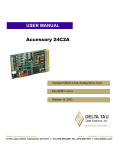
^1 USER MANUAL
^2 Accessory 24P2
^3 Axis Expansion Board
^4 3Ax-603135-xUxx
^5 October 15, 2003
Single Source Machine Control
Power // Flexibility // Ease of Use
21314 Lassen Street Chatsworth, CA 91311 // Tel. (818) 998-2095 Fax. (818) 998-7807 // www.deltatau.com
Software Setup for Tturbo PMAC
1
Copyright Information
© 2003 Delta Tau Data Systems, Inc. All rights reserved.
This document is furnished for the customers of Delta Tau Data Systems, Inc. Other uses are
unauthorized without written permission of Delta Tau Data Systems, Inc. Information contained in
this manual may be updated from time-to-time due to product improvements, etc., and may not
conform in every respect to former issues.
To report errors or inconsistencies, call or email:
Delta Tau Data Systems, Inc. Technical Support
Phone: (818) 717-5656
Fax: (818) 998-7807
Email: support@deltatau.com
Website: http://www.deltatau.com
Operating Conditions
All Delta Tau Data Systems, Inc. motion controller products, accessories, and amplifiers contain
static sensitive components that can be damaged by incorrect handling. When installing or handling
Delta Tau Data Systems, Inc. products, avoid contact with highly insulated materials. Only
qualified personnel should be allowed to handle this equipment.
In the case of industrial applications, we expect our products to be protected from hazardous or
conductive materials and/or environments that could cause harm to the controller by damaging
components or causing electrical shorts. When our products are used in an industrial environment,
install them into an industrial electrical cabinet or industrial PC to protect them from excessive or
corrosive moisture, abnormal ambient temperatures, and conductive materials. If Delta Tau Data
Systems, Inc. products are directly exposed to hazardous or conductive materials and/or
environments, we cannot guarantee their operation.
Accessory 24P2
Table of Contents
INTRODUCTION .......................................................................................................................................................1
Overview .......................................................................................................................................................................1
Features .........................................................................................................................................................................1
Board Configuration ......................................................................................................................................................2
HARDWARE SETUP .................................................................................................................................................3
Position Compare Port Driver IC ..................................................................................................................................3
Switch Configuration.....................................................................................................................................................3
Address DIP Switch S1..............................................................................................................................................3
Jumper Configuration ....................................................................................................................................................4
Position Compare Output Configuration Jumpers....................................................................................................4
Encoder Sample Clock Source Jumpers....................................................................................................................4
Serial ADC Source Jumpers......................................................................................................................................4
Output Disable State Jumpers ...................................................................................................................................5
Resistor Pack Configuration ..........................................................................................................................................5
Termination Resistors ...............................................................................................................................................5
Pull-Up/Pull-Down Resistors....................................................................................................................................5
Connections ...................................................................................................................................................................6
Mounting ...................................................................................................................................................................6
Power Supply Connection .........................................................................................................................................7
Connection to Turbo PMAC......................................................................................................................................7
Machine Port Connections........................................................................................................................................7
Alternate Port Connections .......................................................................................................................................7
SOFTWARE SETUP FOR TURBO PMAC .............................................................................................................9
System Configuration I-Variables .................................................................................................................................9
External Servo IC Enable..........................................................................................................................................9
External Servo IC Type .............................................................................................................................................9
Servo IC Configuration I-Variables...............................................................................................................................9
Servo IC Numbering..................................................................................................................................................9
Servo Channel Numbering ......................................................................................................................................10
Multi-Channel I-Variables ......................................................................................................................................10
Single-Channel I-Variables.....................................................................................................................................11
Encoder Conversion Table I-Variables...................................................................................................................11
Motor Addressing I-Variables.................................................................................................................................12
JUMPER AND SWITCH DESCRIPTIONS...........................................................................................................17
Board Layout ...............................................................................................................................................................17
S1: Board Addressing DIP-Switch Bank.....................................................................................................................18
E11, E12: Output Driver IC Configuration ................................................................................................................19
E13, E14: Encoder Sample Clock Direction................................................................................................................19
E23 – E26: Serial ADC Source Select........................................................................................................................20
E111 – E118: Digital Command Output Disable State...............................................................................................21
CONNECTOR DESCRIPTIONS ............................................................................................................................23
JS1: ADC Channel 1 & 2 Connector ..........................................................................................................................23
JS2: ADC Channel 3 & 4 Connector ..........................................................................................................................24
JS3: ADC Channel 5 6 Connector ..............................................................................................................................24
JS4: ADC Channel 7 & 8 Connector ..........................................................................................................................25
J8 (JEQU): Position Compare Output Connector.......................................................................................................25
J9 (JMACH1): Servo Channel 1 & 2 Connector ........................................................................................................26
J10 (JMACH2): Servo Channel 3 & 4 Connector ......................................................................................................30
J11 (JMACH3): Servo Channel 5 & 6 Connector ......................................................................................................34
J12 (JMACH4): Servo Channel 7 & 8 Connector ......................................................................................................38
J1 (JEXP): Expansion Port Connector........................................................................................................................41
P1: ISA Bus Connector...............................................................................................................................................41
TB1: Standalone Power Supply Terminal Block........................................................................................................41
Table of Contents
i
Accessory 24P2
ii
Table of Contents
Accessory 24P2
INTRODUCTION
Overview
The ACC-24P2 Axis Expansion Board provides four or eight channels of PMAC2-style servo interface
circuitry for Turbo PMAC controllers. Up to four ACC-24P2 boards can be connected to one Turbo
PMAC board, providing up to 32 additional channels of servo interface circuitry.
The ACC-24P2 is a 2/3-sized PC expansion card. It has ISA bus connectors, so it can be mounted in an
ISA expansion slot. The ACC-24P2 does not communicate over the bus; the bus connectors are just a
convenience for mounting the board near the Turbo PMAC when it is in the bus.
The ACC-24P2 board contains no processor; it has 1 or 2 highly integrated 4-channel PMAC2-style
“Servo ICs” with the buffering circuitry and connectors around them.
Features
The ACC-24P2 board can be used with any Turbo PMAC(1) or Turbo PMAC2 board, interfacing through
the Expansion port. It is electrically and software compatible with Turbo PMAC(1)-VME and Turbo
PMAC2-VME, but special mounting would be required. Note that even if the Turbo PMAC itself is a
PMAC(1) with the PMAC(1)-style Servo ICs and interface circuitry, the ACC-24P2 with its PMAC2style Servo ICs and interface circuitry can be connected to it.
The ACC-24P2 supports a wide variety of servo and stepper interfaces:
•
•
•
•
•
Analog +/-10V velocity commands (requires ACC-8A, ACC-8E or equivalent)
Analog +/-10V torque commands (requires ACC-8A, ACC-8E or equivalent)
Sinusoidal analog +/-10V phase current commands (requires ACC-8E or equivalent)
Direct digital pulse-width modulated (PWM) phase voltage commands (requires ACC-8F, ACC-8K,
or equivalent)
Pulse-and-direction commands (requires ACC-8S or equivalent)
A single ACC-24P2 can be used with a regular (non-Turbo) PMAC2 board, but there is no I-variable
support in the regular PMAC2 for the configuration of the Servo ICs on the ACC-24P2. (I-variables I900
– I989 support the setup of the eight channels of the two Servo ICs on board the PMAC2 itself; there is
nothing comparable for the eight channels on an ACC-24P2).
Use of an ACC-24P2 with a regular PMAC2 board requires the assignment of M-variables to the registers
that would be I-variables, and execution of a power-on PLC to set the proper values in these registers.
Introduction
1
Accessory 24P2
Board Configuration
An ACC-24P2 comes standard with one Servo IC providing four servo interface channels, which are
brought out on two 100-pin high-density connectors to an ACC-8 family breakout board or equivalent.
Each channel of servo interface circuitry includes the following:
•
•
•
•
Three output command signal sets, configurable as either:
• Two serial data streams to external DACs, 1 pulse-and-direction
• Three PWM top-and-bottom pairs
3-channel differential/single-ended encoder input
Nine input flags, two output flags
Interface to two external serial ADCs, 8 to 18 bits
Option 1: If Option 1 is ordered, a second Servo IC with four additional servo interface channels is
provided, for a total of eight interface channels on the board, brought out on four 100-pin high-density
connectors.
2
Introduction
Accessory 24P2
HARDWARE SETUP
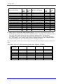
Position Compare Port Driver IC
The position compare output port J8 (JEQU) has a socketed driver IC in a 20-pin DIP socket at
component U5. Three types of ICs can be placed in this socket: a fast CMOS driver, a high-current
sinking driver, and a high-current sourcing driver.
The following table lists the properties of each driver IC:
Part
# of
Pins
Max Voltage
& Current
Output Type
Max
Frequency
E11, E12
Setting
74ACT563
(default)
ULN2803A
UDN2981
20
5V, 10 mA
Totem-Pole (CMOS)
5 MHz
1-2
18
18
24V, 100 mA
24V, 100 mA
Sinking (Open-Collector)
Sourcing (Open-Emitter)
100 kHz
100 kHz
1-2
2-3
When the 18-pin ICs are placed in the 20-pin socket, pin 1 of the IC should be placed in pin 2 of the
socket. This puts the IC at the right end of the socket when the board is the orientation where the text on
the board reads properly.
Switch Configuration
Address DIP Switch S1
S1 is a 4-point DIP switch that sets up the address of the ACC-24P2 in Turbo PMAC’s memory and I/O
map. The setting of these DIP switches must match the addresses used by Turbo PMAC. No two ACC24P2 boards connected to the same Turbo PMAC may have the same DIP switch address setting, or there
will be an addressing conflict.
Switch S1-3 must be ON on an ACC-24P2 to enable addressing of the board by a Turbo PMAC. It must
be OFF to enable addressing of the board by a non-Turbo PMAC2 board. In this case the settings of S1-1
and S1-2 do not matter.
Switch S1-4 controls whether loss-of-encoder fault can be read by the Turbo PMAC or not. If E20 is ON,
these encoder faults can be read at the following addresses:
•
•
•
•
1st ACC-24P2:
2nd ACC-24P2:
3rd ACC-24P2:
Y:$078F00 bits 16-23
Y:$079F00 bits 16-23
Y:$07AF00 bits 16-23
4th ACC-24P2:
Y:$07BF00 bits 16-23
Hardware Setup
3
Accessory 24P2
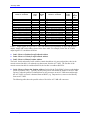
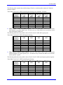
The settings of switches S1-1 and S1-2 define the address of the board in Turbo PMAC’s address space.
This in turn defines the “number” of the Servo IC(s) on the board, and the I-variable numbers in the
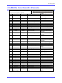
Turbo PMAC that configure the IC(s). The following table lists the possible settings:
S1-1
S1-2
Board
No.
1ST IC
NO.
2ND
IC
NO.
1ST IC
I-Var.
Range
2ND IC
I- Var.
Range
1ST IC
Base
Address
2ND IC
Base
Address
ON
OFF
ON
OFF
ON
ON
OFF
OFF
1ST
2ND
3RD
4TH
2
4
6
8
3
5
7
9
I7200-I7299
I7400-I7499
I7600-I7699
I7800-I7899
I7300-I7399
I7500-I7599
I7700-I7799
I7900-I7999
$078200
$079200
$07A200
$07B200
$078300
$079300
$07A300
$07B300
It is suggested, but not required, that the boards be assigned in order. That is, if there are two ACC-24P2
boards in the system, set up the one closest to the Turbo PMAC as the “1st” board, and the next one as the
“2nd” board.
Jumper Configuration
Position Compare Output Configuration Jumpers
CAUTION
An incorrect setting of either of these jumpers can permanently damage the driver IC.
Jumpers E11 and E12 configure the hardware of the outputs on the JEQU (J8) Position Compare port.
They must be set properly for the port’s socketed driver IC in U5.
The ACC-24P2 normally is shipped with a 74ACT563 (or equivalent) CMOS driver IC. For this IC,
jumpers E11 and E12 must both connect pins 1 and 2.
If the standard output driver is replaced with a ULN2803A (or equivalent) sinking output driver IC,
jumpers E11 and E12 must both connect pins 1 and 2.
If the standard output driver is replaced with a UDN2981A (or equivalent) sourcing output driver IC,
jumpers E11 and E12 must both be moved to connect pins 2 and 3.
Encoder Sample Clock Source Jumpers
Jumpers E13 and E14 control the source of the SCLK encoder sampling clock for each servo IC. The
default setting of no jumper installed means that the SCLK signal comes from the servo IC and is output
on the JMACH connectors. This setting is suitable for all but a few very special applications.
If Switch S1-4 is OFF, these fault bits cannot be read by the Turbo PMAC, and another board, such as an
ACC-14D or ACC-36P can be used in that address space.
Serial ADC Source Jumpers
Jumpers E23, E24, E25, and E26 determine the source of serial ADC signals for each pair of channels on
the ACC-24P2.
If the jumper is OFF (default), the serial ADC signals for the two channels come in through the 100-pin
JMACH servo interface connector. This setting is used for digital current feedback when using directPWM power block amplifiers. It is also used for inputs from an ACC-28B ADC board when connected
to the ACC-24P2 board through an ACC-8T board.
If the jumper is ON, the serial ADC signals for the two channels come in through the 16-pin JSx header
on the board. This setting is used for the ACC-28B board when connected directly to the ACC-24P2
board’s JSx connector.
4
Hardware Setup
Accessory 24P2
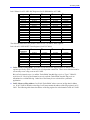
The following table lists the connectors used for each jumper:
Jumper
Source when OFF
Source when ON
E23
E24
E25
E26
J9 (JMACH1)
J10 (JMACH2)
J11 (JMACH3)
J12 (JMACH4)
JS1
JS2
JS3
JS4
Output Disable State Jumpers
Jumpers E111 through E118 control the hardware state of the digital command output signals for each
channel when the amplifier enable signal for that channel is in the “disable” state (false). Jumper E11n (n
= 1 to 8) controls the output signals for Channel ‘n’ on the board.
If E11n is OFF (default), the command output signals for Channel ‘n’ are still active when the amplifier
enable signal is in the “disable” state. The Turbo PMAC software should be commanding a net zero
command to be output on these signals, and the amplifier enable signal should be used by the amplifier so
that no command output will cause action if it is receiving a “disable” signal. This OFF setting must be
used when DAC output format is selected for the channel.
If E11n is ON, the command output signals for Channel ‘n’ are “tri-stated” when the amplifier enable
signal is in the “disable” state. Typically, this setting is used only with direct-PWM power-block
amplifiers that do not use amplifier enable to gate the PWM signals, and in which the zero-command
format of 50% top on-time, and 50% bottom on-time cannot be tolerated in the disable state.
Resistor Pack Configuration
Termination Resistors
The ACC-24P2 provides sockets for termination resistors on differential input pairs coming into the
board. As shipped, there are no resistor packs in these sockets. If these signals are brought long distances
into the ACC-24P2 board and ringing at signal transitions is a problem, SIP resistor packs may be
mounted in these sockets to reduce or eliminate the ringing.
All termination resistor packs are the types that have independent resistors (no common connection) with
each resistor using 2 adjacent pins. The following table shows which packs are used to terminate each
input device:
Input
Pack
Pack Size
Input
Pack
Pack Size
Encoder 1
Encoder 2
Encoder 3
Encoder 4
Encoder 5
Encoder 6
Encoder 7
Encoder 8
SCLK12&34
RP79
RP80
RP92
RP91
RP137
RP138
RP148
RP149
RP97
6-pin
6-pin
6-pin
6-pin
6-pin
6-pin
6-pin
6-pin
6-pin
ADC 1 & 2
ADC 3 & 4
ADC 5 & 6
ADC 7 & 8
Fault 1 & 2
Fault 3 & 4
Fault 5 & 6
Fault 7 & 8
SCLK56&78
RP81
RP90
RP144
RP154
RP82
RP89
RP145
RP155
RP157
8-pin
8-pin
8-pin
8-pin
6-pin
6-pin
6-pin
6-pin
6-pin
Pull-Up/Pull-Down Resistors
The differential input signal pairs to the ACC-24P2 have user-configurable pull-up/pull-down resistor
networks to permit the acceptance of either single-ended or differential signals in one setting, or the
detection of lost differential signals in another setting.
The ‘+’ inputs of each differential pair each have a hard-wired 1k pull-up resistor to +5V. This cannot be
changed.
Hardware Setup
5
Accessory 24P2
The ‘-‘ inputs of each differential pair each have a hard-wired 2.2k resistor to +5V; each also has another
2.2k resistor as part of a socketed resistor pack that can be configured as a pull-up resistor to +5V, or a
pull-down resistor to GND.
If this socketed resistor is configured as a pull-down resistor (the default configuration), the combination
of pull-up and pull-down resistors on this line acts as a voltage divider, holding the line at +2.5V in the
absence of an external signal. This configuration is required for single-ended inputs using the ‘+’ lines
alone; it is desirable for unconnected inputs to prevent the pick-up of spurious noise; it is permissible for
differential line-driver inputs.
If this socketed resistor is configured as a pull-up resistor (by reversing the SIP pack in the socket), the
two parallel 2.2k resistors act as a single 1.1k pull-up resistor, holding the line at +5V in the absence of an
external signal. This configuration is required if encoder-loss detection is desired; it is required if
complementary open-collector drivers are used; it is permissible for differential line-driver inputs even
without encoder loss detection.
If Pin 1 of the resistor pack, marked by a dot on the pack, matches Pin 1 of the socket, marked by a wide
white line on the front side of the board, and a square solder pin on the back side of the board, then the
pack is configured as a bank of pull-down resistors. If the pack is reversed in the socket, it is configured
as a bank of pull-up resistors.
The following table lists the pull-up/pull-down resistor pack for each input device:
Device
Resistor Pack
Device
Resistor Pack
Encoder 1
Encoder 2
Encoder 3
Encoder 4
Encoder 5
Encoder 6
Encoder 7
Encoder 8
RP74
RP75
RP85
RP86
RP139
RP140
RP150
RP151
ADC/Fault1&2
ADC/FAULT3&4
ADC/Fault5&6
ADC/Fault7&8
SCLK12&34
SCLK56&78
RP76
RP87
RP143
RP65
RP98
RP156
Connections
Mounting
The ACC-24P2 can be mounted in one of three ways: in the ISA bus, or using standoffs.
•
•
ISA bus: To mount in the ISA bus, simply insert the P1 card-edge connector into the ISA socket. If
there is a standard PC-style housing, a bracket at the end of the ACC-24P2 board can be used to
screw into the housing to hold the board down firmly.
Standoffs: At each of the 4 corners of the ACC-24P2 board, there are mounting holes that can be
used to mount the board on standoffs.
Note
The ACC-24P2 board does not do any communication through the bus connector;
the connector is used simply for mounting, and, if the bus connector is electrically
active, for power supply. Even in standalone applications, passive backplane
boards can be very useful for mounting and power supply.
6
Hardware Setup
Accessory 24P2
Power Supply Connection
The ACC-24P2 requires only 5V power: 1A in a 4-channel configuration, 2A in an 8-channel
configuration (with Option 1). This power can be provided in several ways:
•
•
•
Bus connector: If the ACC-24P2 is mounted in an electrically active ISA bus slot, it automatically
draws its 5V power from the bus.
Terminal block: The TB1 2-point terminal block can be used to bring in 5V power, especially in
standalone applications. Point 1 is GND; Point 2 is +5V.
JMACH connectors: Up to 1A may be brought in through each 100-pin JMACH connector from an
ACC-8 board or its equivalent, provided the cable is 500 mm (20 in) or less in length.
Connection to Turbo PMAC
The ACC-24P2 connects to the Turbo PMAC through the 50-pin J1 header on the ACC-24P2. A short
flat cable connects this to the JEXP header on the Turbo PMAC. If multiple ACC-24 boards are
connected to a single Turbo PMAC board, they must be connected on a single daisy-chain cable. Total
length of this cable should not exceed 300mm (12 in).
Machine Port Connections
ACC-24P2 has a 100-pin high-density header for each pair of servo interface channels. Through this
connector pass all of the digital signals to and from the amplifier, encoder, and flags for the two channels.
Typically, this header is connected with a matching Delta Tau ACC-8 family 2-channel breakout board or
equivalent through a provided 100-pin flat cable.
The machine port connectors are:
•
•
•
•
J9 (JMACH1)
J10 (JMACH2)
Board Channels 1 & 2
Board Channels 3 & 4
J11 (JMACH3)
J12 (JMACH4)
Board Channels 5 & 6 (Option 1 required)
Board Channels 7 & 8 (Option 1 required)
Alternate Port Connections
ACC-24P2 has a 16-pin header that provides alternate pinout for several signals associated with each pair
of servo interface channels. These signals include the ADC clock, strobe, and data; the amplifier enable
outputs, and the position compare outputs.
The main use of the alternate port connector is to provide a direct interface to an ACC-28B 2-channel or
4-channel A/D converter board. The ACC-28B can be connected directly to the alternate port connector
on the ACC-24P2 through a 16-pin flat cable provided with the ACC-28B.
In order to use ADC inputs on the alternate connector, a jumper for the connector must be installed. If the
jumper is OFF, the ACC-24P2 will take its ADC inputs from the matching 100-pin machine port
connector.
The alternate port connectors and their control jumpers are:
•
•
•
•
JS1
Board Channels 1 & 2
Jumper E23
JS2
JS3
JS4
Board Channels 3 & 4
Board Channels 5 & 6
Board Channels 7 & 8
Jumper E24
Jumper E25 (Option 1 required)
Jumper E26 (Option 1 required)
Hardware Setup
7
Accessory 24P2
8
Hardware Setup
Accessory 24P2
SOFTWARE SETUP FOR TURBO PMAC
Use of the ACC-24P2 requires the proper setup of several I-variables on the Turbo PMAC. These
settings are discussed in this section. More detailed descriptions of the variables are given in the Turbo
PMAC Software Reference.
System Configuration I-Variables
External Servo IC Enable
Turbo PMAC variable I65 tells the controller which external devices containing Servo ICs, such as the
ACC-24P2, are present in the system. I65 is a 4-bit value, with each bit representing 1 of the 4 possible
devices that can be connected to a Turbo PMAC. The bit must be set to 1 to tell the Turbo PMAC
software that the device is present.
•
•
•
•
Bit 0, with a value of 1, specifies whether the 1st device is present
Bit 1, with a value of 2, specifies whether the 2nd device is present
Bit 2, with a value of 4, specifies whether the 3rd device is present
Bit 3, with a value of 8, specifies whether the 4th device is present
An ACC-24P2 can be the first, second, third, or fourth device, depending on the setting of DIP switches
S1-1 and S1-2.
Normally these external devices are added in order, so I65 takes one of four values:
•
•
•
•
1st external device alone: I65=1
1st and 2nd external devices: I65=3
1st, 2nd, and 3rd external devices: I65=7
1st, 2nd, 3rd, and 4th external devices: I65=15
External Servo IC Type
Turbo PMAC variable I66 tells the controller which type of IC is present on a given external device. I66
is a 4-bit value, with each bit representing 1 of the 4 possible devices that can be connected to a Turbo
PMAC. The bit is set to 0 if the device contains “Type 0” PMAC(1)-style DSPGATE Servo ICs; it is set
to 1 if the device contains “Type 1” PMAC2-style DSPGATE1 Servo ICs.
The ACC-24P2 contains the “Type 1” PMAC2-style Servo ICs, so the bit of I66 for the ACC-24P2 must
be set to 1 for proper operation.
•
•
•
•
Bit 0, with a value of 1, is set to 1 if the 1st ACC-24P2 is present
Bit 1, with a value of 2, is set to 1 if the 2nd ACC-24P2 is present
Bit 2, with a value of 4, is set to 1 if the 3rd ACC-24P2 is present
Bit 3, with a value of 8, is set to 1 if the 4th ACC-24P2 is present
Servo IC Configuration I-Variables
Turbo PMAC I-variables in the range I7000 – I7999 control the configuration of the Servo ICs. The
hundred’s digit represents the number of the Servo IC (0 to 9) in the system. Servo ICs 0 and 1 are (or
can be) on board the Turbo PMAC board itself. Servo ICs 2 through 9 are (or can be) on external devices
such as the ACC-24P2.
Servo IC Numbering
The number ‘m’ of the Servo IC on the ACC-24P2 board is dependent on the addressing of the board with
DIP switches S1-1 and S1-2, which place the board as the 1st, 2nd, 3rd, or 4th external device:
Hardware Setup
9
Accessory 24P2
•
•
•
•
1st ACC-24P2:
2nd ACC-24P2:
3rd ACC-24P2:
Servo IC 2 (Standard); Servo IC 3 (Option 1)
Servo IC 4 (Standard); Servo IC 5 (Option 1)
Servo IC 6 (Standard); Servo IC 7 (Option 1)
4th ACC-24P2:
Servo IC 8 (Standard); Servo IC 9 (Option 1)
The “Standard” Servo IC on an ACC-24P2 occupies Channels 1 – 4 on the board, using connectors
JMACH1, JMACH2, JS1, and JS2. The “Option 1” Servo IC on an ACC-24P2 occupies Channels 5 – 8
on the board, using connectors JMACH3, JMACH4, JS3, and JS4.
For example, the “Standard” Servo IC on the 1st ACC-24P2 is Servo IC 2 to Turbo PMAC and is
configured by variables I7200 – I7299.
Servo Channel Numbering
Each Servo IC has 4 channels of servo interface circuitry. The ten’s digit ‘n’ of the I-variable configuring
the IC represents the channel number on the IC (n = 1 to 4). For example, Channel 1 of the “Standard”
Servo IC on the 1st ACC-24P2 is configured by variables I7210 – I7219. These channel-specific Ivariables are represented generically as I7mn0 – I7mn9, where ‘m’ represents the Servo IC number (0 –
9) and ‘n’ represents the IC channel number (1 – 4).
The Channels 1 – 4 on the “Standard” Servo IC of an ACC-24P2 correspond to Channels 1 – 4,
respectively, on the ACC-24P2 board itself. The Channels 1 – 4 on the “Option 1” Servo IC on an ACC24P2 correspond to Channels 5 – 8, respectively, on the ACC-24P2 board.
I-variables in the I7000s for which the ten’s digit is ‘0’ (“Channel 0”) affect all 4 channels of the
PMAC2-style Servo IC on the ACC-24P2. These multi-channel I-variables are represented generically as
I7m00 – I7m09.
Multi-Channel I-Variables
There are several multi-channel I-variables that must be set up properly for proper operation of the ACC24P2 in a Turbo PMAC system. The most important are:
•
•
I7m07: Servo IC m Phase/Servo Clock Direction: This variable should be set to 3 for any Servo IC
on an ACC-24P2 so it inputs its phase and servo clocks from signals generated on the Turbo PMAC
itself.
I7m00: Servo IC m MaxPhase/PWM Frequency Control: Typically this will be set to the same
value as the variable that controls the system clocks: I7000 on a non-Ultralite Turbo PMAC2, or
I6800 on a Turbo PMAC2 Ultralite. If a different PWM frequency is desired, or the ACC-24P2 is
used with a Turbo PMAC(1) in which the system clock frequencies are set by jumpers, then the
following constraint should be observed in setting this variable:
2 * PWMFreq( kHz )
= { Integer }
PhaseFreq
•
I7m01: Servo IC m Phase Clock Frequency Control: Even though the IC is receiving an external
phase clock (see I7m07, above), it is usually best to create the same internal phase clock frequency in
the Servo IC. This yields the following constraint:
I 7 m 00 * ( I 7 m 01 + 1 ) = I 7000 * ( I 7001 + 1 ) {non-Ultralite Turbo PMAC2}
I 7 m00 * ( I 7 m01 + 1 ) = I 6800 * ( I 6801 + 1 )
{Turbo PMAC2 Ultralite}
Solving for I7m01, we get
10
Hardware Setup
Accessory 24P2
I 7 m01 =
I 7000 * ( I 7001 + 1 )
−1
{non Ultralite PMAC2}
I 7 m00
I 7 m01 =
I 6800 * ( I 6801 + 1 )
− 1 {Turbo PMAC2 Ultralite}
I 7 m00
If I7m00 is the same as I7000 or I6800, I7m01 will be the same as I7001 or I6801. If the ACC-24P2
is interfaced to a Turbo PMAC(1) board, it should be set by calculation to obtain the same phase
clock frequency as that set by the jumpers on the Turbo PMAC(1).
•
•
I7m02: Servo IC m Servo Clock Frequency Control: Even though the IC is receiving an external
servo clock (see I7m07, above), it is usually best to create the same internal servo clock frequency in
the Servo IC. This means that I7m02 for the IC should be set the same as I7002 on a non-Ultralite
Turbo PMAC2, or the same as I6802 on a Turbo PMAC2 Ultralite. When connected to a Turbo
PMAC(1), I7m02 should create the same division from the phase clock as jumpers E3 – E6 do on the
Turbo PMAC(1).
I7m03: Servo IC m Hardware Clock Frequency Control: The hardware clock frequencies for the
Servo IC should be set according to the devices attached to it. There is no reason that these
frequencies have to be the same between ICs. There is seldom a reason to change this value from the
default.
Single-Channel I-Variables
The single-channel setup I-variables for Channel ‘n’ of Servo IC ‘m’ work exactly the same on an ACC24P2 as they do on a Turbo PMAC2 itself. Each Servo IC has 4 channels ‘n’, numbered 1 to 4. For the
first (standard) Servo IC on the ACC-24P2, the channel numbers 1 – 4 on the Servo IC are the same as
the channel numbers 1 – 4 on the board. For the second (optional) Servo IC on the ACC-24P2, the
channel numbers 1 – 4 on the Servo IC correspond to board channel numbers 5 – 8. The most important
variables are:
•
•
•
•
I7mn0: Servo IC m Channel n Encoder Decode Control: I7mn0 is typically set to 3 or 7 for “x4”
quadrature decode, depending on which way is “up”. If the channel is used for open-loop stepper
drive, I7mn0 is set to 8 to accept internal pulse-and-direction, or to 0 to accept external pulse-anddirection (e.g. from an ACC-8S). It is set to 12 if the channel is used for MLDT feedback.
I7mn2: Servo IC m Channel n Capture Control: I7mn2 determines whether the encoder index
channel, an input flag, or both, are used for the capture of the encoder position.
I7mn3: Servo IC m Channel n Capture Flag Select: I7mn3 determines which input flag is used
for encoder capture, if one is used.
I7mn6: Servo IC m Channel n Output Mode Select: I7mn6 determines whether the A and B
outputs are DAC or PWM, and whether the C output is PFM (pulse-and-direction) or PWM. It is
typically set either to 0, for 3-phase PWM, or to 3 for DACs and PFM.
Encoder Conversion Table I-Variables
To use feedback or master position data from an ACC-24P2, entries must be added to the encoder
conversion table (ECT) using I-variables I8000 – I8191 to address and process this data. The default
conversion table in the Turbo PMAC does not contain these entries; it only contains entries for the 8
channels on board the Turbo PMAC.
The position data obtained through an ACC-24P2 board is usually an incremental encoder feedback, and
occasionally an A/D converter feedback from an ACC-28B board connected through the ACC-24P2.
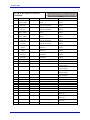
The ECT entries for ACC-24P2 incremental encoder channels are shown in the following table:
Hardware Setup
11
Accessory 24P2
Encoder
Channel #
1st
ACC-24P2
2nd
ACC-24P2
3rd
ACC-24P2
4th
ACC-24P2
Channel 1
Channel 2
Channel 3
Channel 4
Channel 5
Channel 6
Channel 7
Channel 8
$mF8200
$mF8208
$mF8210
$mF8218
$mF8300
$mF8308
$mF8310
$mF8318
$mF9200
$mF9208
$mF9210
$mF9218
$mF9300
$mF9308
$mF9310
$mF9318
$mFA200
$mFA208
$mFA210
$mFA218
$mFA300
$mFA308
$mFA310
$mFA318
$mFB200
$mFB208
$mFB210
$mFB218
$mFB300
$mFB308
$mFB310
$mFB318
The first hexadecimal digit in the entry, represented by ‘m’ in the table, is a ‘0’ for the most common 1/T
timer-based extension of digital incremental encoders; it is an ‘8’ for the parallel-data extension of analog
incremental encoders; it is a ‘C’ for no extension of an incremental encoder.
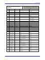
The ECT entries for ACC-28B A/D converters read through an ACC-24P2 are shown in the following
table:
Register
1st ACC24P2
2nd ACC24P2
3rd ACC24P2
4th ACC24P2
ADC 1A
ADC 1B
ADC 2A
ADC 2B
ADC 3A
ADC 3B
ADC 4A
ADC 4B
ADC 5A
ADC 5B
ADC 6A
ADC 6B
ADC 7A
ADC 7B
ADC 8A
ADC 8B
$mF8205
$mF8206
$mF820D
$mF820E
$mF8215
$mF8216
$mF821D
$mF821E
$mF8305
$mF8306
$mF830D
$mF830E
$mF8315
$mF8316
$mF831D
$mF831E
$mF9205
$mF9206
$mF920D
$mF920E
$mF9215
$mF9216
$mF921D
$mF921E
$mF9305
$mF9306
$mF930D
$mF930E
$mF9315
$mF9316
$mF931D
$mF931E
$mFA205
$mFA206
$mFA20D
$mFA20E
$mFA215
$mFA216
$mFA21D
$mFA21E
$mFA305
$mFA306
$mFA30D
$mFA30E
$mFA315
$mFA316
$mFA31D
$mFA31E
$mFB205
$mFB206
$mFB20D
$mFB20E
$mFB215
$mFB216
$mFB21D
$mFB21E
$mFB305
$mFB306
$mFB30D
$mFB30E
$mFB315
$mFB316
$mFB31D
$mFB31E
The first hexadecimal digit of the entry, represented by ‘m’ in the above table, is a ‘1’ if the ADC data is
processed directly, without integration; it is a ‘5’ if the data is integrated in the conversion. If the entry
integrates the data, there is a second line in the entry – another I-variable – that specifies the bias of the
A/D converter.
Motor Addressing I-Variables
For a Turbo PMAC motor to use the servo interface circuitry of the ACC-24P2, several of the addressing
I-variables for the motor must contain the addresses of registers in the ACC-24P2, or the addresses of
encoder conversion table registers containing data processed from the ACC-24P2. These I-variables can
include:
•
12
Ixx02: Motor xx Command Output Address: Ixx02 tells Turbo PMAC where to write its
command outputs for Motor xx. If ACC-24P2 is to create the command signals, Ixx02 must contain
the address of the register. The following table shows the address of the ‘A’ output register for each
channel of each ACC-24P2. These addresses can be used for single analog outputs, double analog
outputs, or direct PWM outputs.
Hardware Setup
Accessory 24P2
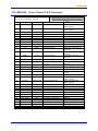
ACC-24P2 Register:
Board No. & Channel
Address /
Ixx02
Value
PMAC2
Default
for:
ACC-24P2 Register:
Board No. & Channel
Address /
Ixx02
Value
1st ACC-24P/V2 DAC/PWM1A
1st ACC-24P/V2 DAC/PWM2A
1st ACC-24P/V2 DAC/PWM3A
1st ACC-24P/V2 DAC/PWM4A
1st ACC-24P/V2 DAC/PWM5A
1st ACC-24P/V2 DAC/PWM6A
1st ACC-24P/V2 DAC/PWM7A
1st ACC-24P/V2 DAC/PWM8A
2nd ACC-24P/V2 DAC/PWM1A
2nd ACC-24P/V2 DAC/PWM2A
2nd ACC-24P/V2 DAC/PWM3A
2nd ACC-24P/V2 DAC/PWM4A
2nd ACC-24P/V2 DAC/PWM5A
2nd ACC-24P/V2 DAC/PWM6A
2nd ACC-24P/V2 DAC/PWM7A
2nd ACC-24P/V2 DAC/PWM8A
$078202
$07820A
$078212
$07821A
$078302
$07830A
$078312
$07831A
$079202
$07920A
$079212
$07921A
$079302
$07930A
$079312
$07931A
I902
I1002
I1102
I1202
I1302
I1402
I1502
I1602
I1702
I1802
I1902
I2002
I2102
I2202
I2302
I2402
3rd ACC-24P/V2 DAC/PWM1A
3rd ACC-24P/V2 DAC/PWM2A
3rd ACC-24P/V2 DAC/PWM3A
3rd ACC-24P/V2 DAC/PWM4A
3rd ACC-24P/V2 DAC/PWM5A
3rd ACC-24P/V2 DAC/PWM6A
3rd ACC-24P/V2 DAC/PWM7A
3rd ACC-24P/V2 DAC/PWM8A
4th ACC-24P/V2 DAC/PWM1A
4th ACC-24P/V2 DAC/PWM2A
4th ACC-24P/V2 DAC/PWM3A
4th ACC-24P/V2 DAC/PWM4A
4th ACC-24P/V2 DAC/PWM5A
4th ACC-24P/V2 DAC/PWM6A
4th ACC-24P/V2 DAC/PWM7A
4th ACC-24P/V2 DAC/PWM8A
$07A202
$07A20A
$07A212
$07A21A
$07A302
$07A30A
$07A312
$07A31A
$07B202
$07B20A
$07B212
$07B21A
$07B302
$07B30A
$07B312
$07B31A
PMAC
2
Default
for:
I2502
I2602
I2702
I2802
I2902
I3002
I3102
I3202
---------
If the ‘C’ output register for a given ACC-24P2 and channel is used (primarily for pulse and direction
output), simply add 2 to the address shown in the above table. For example, on the first ACC-24P2,
output register 1C is at address $078204.
•
•
•
Ixx03: Motor xx Position-Loop Feedback Address
Ixx04: Motor xx Velocity-Loop Feedback Address
Ixx05: Motor xx Master Position Address
The Ixx03, Ixx04, and usually Ixx05 variables contain the address of a processed position value in the
encoder conversion table, even when the raw data comes from the ACC-24P2. The first line of the
encoder conversion table is at address $003501; the last line is at address $0035C0.
•
Ixx10: Motor xx Power-On Position Address: Ixx10 tells the Turbo PMAC where to read absolute
power-on position, if any. Typically, the only times Ixx10 will contain the address of an ACC-24P2
register is when the position is obtained from an A/D converter on an ACC-28B connected through
the ACC-24P2, or when it is obtained from an MLDT (e.g. TemposonicsTM) sensor excited directly
from an ACC-24P2.
The following table shows the possible values of Ixx10 for ACC-28B A/D converters:
Hardware Setup
13
Accessory 24P2
Ixx10 Values for ACC-24P2 ADC Registers (Ixx95=$B10000 for ACC-28B)
Register
1st ACC-24P2
2nd ACC-24P2
3rd ACC-24P2
4th ACC-24P2
ADC 1A
ADC 1B
ADC 2A
ADC 2B
ADC 3A
ADC 3B
ADC 4A
ADC 4B
ADC 5A
ADC 5B
ADC 6A
ADC 6B
ADC 7A
ADC 7B
ADC 8A
ADC 8B
$078205
$078206
$07820D
$07820E
$078215
$078216
$07821D
$07821E
$078305
$078306
$07830D
$07830E
$078315
$078316
$07831D
$07831E
$079205
$079206
$07920D
$07920E
$079215
$079216
$07921D
$07921E
$079305
$079306
$07930D
$07930E
$079315
$079316
$07931D
$07931E
$07A205
$07A206
$07A20D
$07A20E
$07A215
$07A216
$07A21D
$07A21E
$07A305
$07A306
$07A30D
$07A30E
$07A315
$07A316
$07A31D
$07A31E
$07B205
$07B206
$07B20D
$07B20E
$07B215
$07B216
$07B21D
$07B21E
$07B305
$07B306
$07B30D
$07B30E
$07B315
$07B316
$07B31D
$07B31E
The following table shows the possible values of Ixx10 for MLDT timer registers:
Ixx10 for ACC-24P2 MLDT Timer Registers (Ixx95=$170000)
•
MLDT Timer
Channel #
1st ACC-24P2
2nd ACC-24P2
3rd ACC-24P2
4th ACC-24P2
Channel 1
Channel 2
Channel 3
Channel 4
Channel 5
Channel 6
Channel 7
Channel 8
$078200
$078208
$078210
$078218
$078300
$078308
$078310
$078318
$079200
$079208
$079210
$079218
$079300
$079308
$079310
$079318
$07A200
$07A208
$07A210
$07A218
$07A300
$07A308
$07A310
$07A318
$07B200
$07B208
$07B210
$07B218
$07B300
$07B308
$07B310
$07B318
Ixx24: Motor xx Flag Mode. Ixx24 how to read and use the flags for Motor xx that are in the
register specified by Ixx25. Ixx24 is a set of independent control bits. There are two bits that must be
set correctly to use a flag set on an ACC-24P2.
Bit 0 of Ixx24 must be set to 1 to tell the Turbo PMAC that this flag set is in a “Type 1” PMAC2style Servo IC. Bit 18 of Ixx24 must be set to 0 to tell the Turbo PMAC that this flag set is not
transmitted over a MACRO ring. Other bits of Ixx24 may be set as desired for a particular
application.
•
14
Ixx25: Motor xx Flag Address. Ixx25 tells Turbo PMAC where to access its flag data for Motor
xx. If ACC-24P2 is interface to the flags, Ixx25 must contain the address of the flag register in ACC24P2. The following table shows the address of the flag register for each channel of each ACC-24P2.
Hardware Setup
Accessory 24P2
ACC-24P2 Register:
Board No. & Channel
1st ACC-24P/V2 Flag Set 1
1st ACC-24P/V2 Flag Set 2
1st ACC-24P/V2 Flag Set 3
1st ACC-24P/V2 Flag Set 4
1st ACC-24P/V2 Flag Set 5
1st ACC-24P/V2 Flag Set 6
1st ACC-24P/V2 Flag Set 7
1st ACC-24P/V2 Flag Set 8
2nd ACC-24P/V2 Flag Set 1
2nd ACC-24P/V2 Flag Set 2
2nd ACC-24P/V2 Flag Set 3
2nd ACC-24P/V2 Flag Set 4
2nd ACC-24P/V2 Flag Set 5
2nd ACC-24P/V2 Flag Set 6
2nd ACC-24P/V2 Flag Set 7
2nd ACC-24P/V2 Flag Set 8
•
Address
/ Ixx25
Value
PMAC2
Default
for:
$078200
$078208
$078210
$078218
$078300
$078308
$078310
$078318
$079200
$079208
$079210
$079218
$079300
$079308
$079310
$079318
I925
I1025
I1125
I1225
I1325
I1425
I1525
I1625
I1725
I1825
I1925
I2025
I2125
I2225
I2325
I2425
ACC-24P2 Register:
Board No. & Channel
Address /
Ixx25
Value
3rd ACC-24P/V2 Flag Set 1
3rd ACC-24P/V2 Flag Set 2
3rd ACC-24P/V2 Flag Set 3
3rd ACC-24P/V2 Flag Set 4
3rd ACC-24P/V2 Flag Set 5
3rd ACC-24P/V2 Flag Set 6
3rd ACC-24P/V2 Flag Set 7
3rd ACC-24P/V2 Flag Set 8
4th ACC-24P/V2 Flag Set 1
4th ACC-24P/V2 Flag Set 2
4th ACC-24P/V2 Flag Set 3
4th ACC-24P/V2 Flag Set 4
4th ACC-24P/V2 Flag Set 5
4th ACC-24P/V2 Flag Set 6
4th ACC-24P/V2 Flag Set 7
4th ACC-24P/V2 Flag Set 8
PMAC2
Default
for:
$07A200
$07A208
$07A210
$07A218
$07A300
$07A308
$07A310
$07A318
$07B200
$07B208
$07B210
$07B218
$07B300
$07B308
$07B310
$07B318
I2525
I2625
I2725
I2825
I2925
I3025
I3125
I3225
---------
Ixx81: Motor xx Power-On Phase Position Address. Ixx81 tells Turbo PMAC2 where to read
absolute power-on position for motor phase commutation if any. Typically, it will contain the address
of an ACC-24P2 register for only two types of absolute phasing sensors. The hall-effect
commutation sensors (or their optical equivalents) connected to the U, V, and W input flags on an
ACC-24P2 channel, or the encoder counter filled by simulated quadrature from a Yaskawa absolute
encoder connected to the ACC-24P2 through an ACC-8D Option 9 board.
The following table contains the possible settings of Ixx81 for hall sensor absolute position with an ACC24P2:
Turbo PMAC Ixx81 ACC-24P2 Hall Phasing Settings (Ix91=$800000 - $FF0000)
Hall Flag
Channel #
1st ACC-24P2
2nd ACC-24P2
3rd ACC-24P2
4th ACC-24P2
Channel 1
Channel 2
Channel 3
Channel 4
Channel 5
Channel 6
Channel 7
Channel 8
$078200
$078208
$078210
$078218
$078300
$078308
$078310
$078318
$079200
$079208
$079210
$079218
$079300
$079308
$079310
$079318
$07A200
$07A208
$07A210
$07A218
$07A300
$07A308
$07A310
$07A318
$07B200
$07B208
$07B210
$07B218
$07B300
$07B308
$07B310
$07B318
Hardware Setup
15
Accessory 24P2
The following table contains the possible settings of Ixx81 to read the encoder counters for Yaskawa
absolute encoders:
Turbo PMAC Ixx81 ACC-24P2 Encoder Register Settings (Ix91=$480000 - $580000)
Encoder
Register
Channel #
1st ACC24P2
2nd ACC24P2
3rd ACC24P2
4th ACC24P2
Channel 1
Channel 2
Channel 3
Channel 4
Channel 5
Channel 6
Channel 7
Channel 8
$078201
$078209
$078211
$078219
$078301
$078309
$078311
$078319
$079201
$079209
$079211
$079219
$079301
$079309
$079311
$079319
$07A201
$07A209
$07A211
$07A219
$07A301
$07A309
$07A311
$07A319
$07B201
$07B209
$07B211
$07B219
$07B301
$07B309
$07B311
$07B319
•
Ixx82: Motor xx Current Feedback Address. Ixx82 tells Turbo PMAC where to get its currentloop feedback every phase update cycle. If Ixx82 is set to 0, Turbo PMAC does not perform currentloop calculations for Motor xx.
The following table shows the possible values of Ixx82 for ACC-24P2 ADC register pairs:
Turbo PMAC Ixx82 ACC-24P2 ADC Register Settings
•
ADC
Register
Channel #
1st ACC24P2
2nd ACC24P2
3rd ACC24P2
4th ACC24P2
Channel 1
Channel 2
Channel 3
Channel 4
Channel 5
Channel 6
Channel 7
Channel 8
$078206
$07820E
$078216
$07821E
$078306
$07830E
$078316
$07831E
$079206
$07920E
$079216
$07921E
$079306
$07930E
$079316
$07931E
$07A206
$07A20E
$07A216
$07A21E
$07A306
$07A30E
$07A316
$07A31E
$07B206
$07B20E
$07B216
$07B21E
$07B306
$07B30E
$07B316
$07B31E
Ixx83: Motor xx Phase Position Address. Ixx83 tells Turbo PMAC where to get its commutation
position feedback every phase update cycle. This almost always contains the address of an encoder
“phase position” register.
The following table shows the possible values of Ixx83 for ACC-24P2 encoder phase position registers:
Turbo PMAC Ixx83 ACC-24P2 Encoder Register Settings
16
Encoder
Register
Channel #
1st ACC24P2
2nd ACC24P2
3rd ACC24P2
4th ACC24P2
Channel 1
Channel 2
Channel 3
Channel 4
Channel 5
Channel 6
Channel 7
$078201
$078209
$078211
$078219
$078301
$078309
$078311
$079201
$079209
$079211
$079219
$079301
$079309
$079311
$07A201
$07A209
$07A211
$07A219
$07A301
$07A309
$07A311
$07B201
$07B209
$07B211
$07B219
$07B301
$07B309
$07B311
Channel 8
$078319
$079319
$07A319
$07B319
Hardware Setup
Accessory 24P2
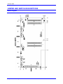
JUMPER AND SWITCH DESCRIPTIONS
Board Layout
Jumper and Switch Descriptions
17
Accessory 24P2
S1: Board Addressing DIP-Switch Bank
Switch
Location
S1-1
B-1
Board Expansion Port Address Select:
ON
B-1
Use S1-1 and S1-2 select ACC-24P2 address on
Turbo PMAC’s expansion port according to
following table
Board Expansion Port Address Select:
ON
B-1
Use S1-1 and S1-2 select ACC-24P2 address on
Turbo PMAC’s expansion port according to
following table
Board Expansion Port Address Enable:
ON
S1-2
S1-3
Description
Default
Set S1-3 to ON position when connecting to Turbo
PMAC/PMAC2; enables addressing of multiple
ACC-24 boards with S1-1 and S1-2.
S1-4
B-1
Set S1-3 to OFF position when connecting to
regular (non-Turbo) PMAC2.
Encoder Fault Read Enable:
OFF
Set S1-4 ON to enable Turbo PMAC read of
encoder fault at CS16 select line. Encoder faults
can be read at:
1st ACC-24P2: Y:$078F00 bits 16-23
2nd ACC-24P2: Y:$079F00 bits 16-23
3rd ACC-24P2: Y:$07AF00 bits 16-23
4TH ACC-24P2: Y:$07BF00 bits 16-23
Set S1-4 OFF to disable Turbo PMAC read of
encoder fault, permitting other types of boards at
the above addresses.
Addressing of ACC-24 Boards for Turbo PMAC
18
S1-1
S1-2
S1-3
Board
No.
ON
OFF
ON
OFF
ON
ON
OFF
OFF
ON
ON
ON
ON
1ST
2ND
3RD
4TH
1ST
IC
No.
2
4
6
8
2ND
IC
No.
3
5
7
9
1ST IC
Base
Address
$078200
$079200
$07A200
$07B200
2ND IC
Base
Address
$078300
$079300
$07A300
$07B300
Jumper and Switch Descriptions
Accessory 24P2
E11, E12: Output Driver IC Configuration
E-Point
E11
Location
A-3
Description
JEQU Port Configuration:
Default
1-2 jumpered
CAUTION
Incorrect setting may damage driver IC.
Jump pins 1 to 2 for CMOS (74ACT563) OR
sinking (ULN2803A) driver on Port (default
configuration).
E12
A-3
Jump pins 2 to 3 for sourcing driver (udn2981a) on
port (alternate configuration).
JEQU Port Configuration:
1-2 jumpered
CAUTION
Incorrect setting may damage driver IC.
Jump pins 1 to 2 for CMOS (74ACT563) OR
sinking (ULN2803A) driver on Port (default
configuration).
Jump pins 2 to 3 for sourcing driver (UDN2981A)
on port (alternate configuration)
E13, E14: Encoder Sample Clock Direction
E-Point
E13
Location
A-5
Description
Encoder sample clock direction:
Default
No jumper
Remove jumper to output SCLK generated in first
Servo IC on SCLK_12 and SCLK_34, or to
control direction by software.
Jump pins 1 to 2 to input SCLK signal for first
Servo IC on SCLK_34 and output this signal on
SCLK_12.
E14
A-2
Jump pins 2 to 3 to input SCLK signal for first
Servo IC on SCLK_12 and output this signal on
SCLK_34.
Encoder sample clock direction:
No jumper
Remove jumper to output SCLK generated in
second Servo IC on SCLK_56 and SCLK_78, or
to control direction by software.
Jump pins 1 to 2 to input SCLK signal for second
Servo IC on SCLK_78 and output this signal on
SCLK_56.
Jump pins 2 to 3 to input SCLK signal for second
Servo IC on SCLK_56 and output this signal on
SCLK_78.
Jumper and Switch Descriptions
19
Accessory 24P2
E23 – E26: Serial ADC Source Select
E-Point
Location
E23
A-4
Description
Default
Serial ADC source select:
Remove jumper to read serial ADC data from
JMACH1 (J9) port: for digital current feedback or
ACC-28B connected thru ACC-8T.
E24
A-4
Jump pins 1 and 2 to read serial ADC data from
JS1: for ACC-28B connected directly to JS1.
Serial ADC source select:
Remove jumper to read serial ADC data from
JMACH2 (J10) port: for digital current feedback
or ACC-28B connected thru ACC-8T.
E25
A-1
Jump pins 1 and 2 to read serial ADC data from
JS2: for ACC-28B connected directly to JS2.
Serial ADC source select:
Remove jumper to read serial ADC data from
JMACH3 (J11) port: for digital current feedback
or ACC-28B connected thru ACC-8T.
E26
A-1
Jump pins 1 and 2 to read serial ADC data from
JS3: for ACC-28B connected directly to JS3.
Serial ADC source select:
Remove jumper to read serial ADC data from
JMACH4 (J12) port: for digital current feedback
or ACC-28B connected thru ACC-8T.
Jumper
removed
Jumper
removed
Jumper
removed
Jumper
removed
Jump pins 1 and 2 to read serial ADC data from
JS4: for ACC-28B connected directly to JS4.
20
Jumper and Switch Descriptions
Accessory 24P2
E111 – E118: Digital Command Output Disable State
E-Point
Location
E111
A-4
Description
Digital command output disable state select:
Default
No jumper
Jump pins 1 to 2 to tri-state channel 1 digital
command output signals when amplifier enable
signal is false (this setting used only for PWM
outputs if balanced 50% output is not desired in
disable mode).
E112
A-4
Remove jumper to keep channel 1 digital
command signals enabled (driving) when amplifier
enable signal is false.
Digital command output disable state select:
No jumper
Jump pins 1 to 2 to tri-state channel 2 digital
command output signals when amplifier enable
signal is false (this setting only used for PWM
outputs if balanced 50% output is not desired in
disable mode).
E113
A-5
Remove jumper to keep channel 2 digital
command signals enabled (driving) when amplifier
enable signal is false.
Digital command output disable state select:
No jumper
Jump pins 1 to 2 to tri-state channel 3 digital
command output signals when amplifier enable
signal is false (this setting only used for PWM
outputs if balanced 50% output is not desired in
disable mode).
Remove jumper to keep channel 3 digital
command signals enabled (driving) when amplifier
enable signal is false.
Jumper and Switch Descriptions
21
Accessory 24P2
E-Point
Location
E114
A-5
Description
Default
Digital command output disable state select:
No jumper
Jump pins 1 to 2 to tri-state channel 4 digital
command output signals when amplifier enable
signal is false (this setting only used for PWM
outputs if balanced 50% output is not desired in
disable mode).
E115
A-2
Remove jumper to keep channel 4 digital
command signals enabled (driving) when amplifier
enable signal is false.
Digital command output disable state select:
No jumper
Jump pins 1 to 2 to tri-state channel 5 digital
command output signals when amplifier enable
signal is false (this setting only used for PWM
outputs if balanced 50% output is not desired in
disable mode).
E116
A-2
Remove jumper to keep channel 5 digital
command signals enabled (driving) when amplifier
enable signal is false.
Digital command output disable state select:
No jumper
Jump pins 1 to 2 to tri-state channel 6 digital
command output signals when amplifier enable
signal is false (this setting only used for PWM
outputs if balanced 50% output is not desired in
disable mode).
E117
A-2
Remove jumper to keep channel 6 digital
command signals enabled (driving) when amplifier
enable signal is false.
Digital command output disable state select:
No jumper
Jump pins 1 to 2 to tri-state channel 7 digital
command output signals when amplifier enable
signal is false (this setting only used for PWM
outputs if balanced 50% output is not desired in
disable mode).
E118
A-2
Remove jumper to keep channel 7 digital
command signals enabled (driving) when amplifier
enable signal is false.
Digital command output disable state select:
No jumper
Jump pins 1 to 2 to tri-state channel 8 digital
command output signals when amplifier enable
signal is false (this setting only used for PWM
outputs if balanced 50% output is not desired in
disable mode).
Remove jumper to keep channel 8 digital
command signals enabled (driving) when amplifier
enable signal is false.
22
Jumper and Switch Descriptions
Accessory 24P2
CONNECTOR DESCRIPTIONS
JS1: ADC Channel 1 & 2 Connector
JS1 (16-Pin Connector)
Top View
Pin #
Symbol
Function
1
2
3
4
ADC_CLK1N.C.
SCLK12+
SCLK12-
Output
Output
Output
Description
Converter clock
No Connect
Encoder Clock
Encoder Clock
Notes
Software set frequency
Software set frequency
Software set frequency
5
ADC_STB1Output
Converter Strobe
Software set signal
6
N.C.
No Connect
7
AENA1+
Output
Amplifier Enable
5V high true
8
AENA2+
Output
Amplifier Enable
5V high true
9
EQU1+
Output
Amplifier enable
5V high true
10
EQU2+
Output
Amplifier Enable
5V high true
11
ADC_DAA1+
Input
ADC Input Data
Serial data stream
12
ADC_DAB1+
Input
ADC Input Data
Serial data stream
13
ADC_DAA2+
Input
ADC Input Data
Serial data stream
14
ADC_DAB2+
Input
ADC Input Data
Serial data stream
15
+5V
Output
+5Vdc Supply
Power supply out
16
GND
Common
PMAC Common
Not isolated from digital
The JS1 connector provides alternate connections for several signals associated with servo interface
channels 1 and 2 on the ACC-24P2. These signals are also present on JMACH1 and JEQU. JS1 can be
used to connect directly to an ACC-28B. Jumper E23 must be removed to use the inputs on JS1.
Connector Descriptions
23
Accessory 24P2
JS2: ADC Channel 3 & 4 Connector
JS2 (16-Pin Connector)
Top View
Pin #
Symbol
Function
Description
Notes
1
ADC_CLK3Output
Converter Clock
Software set frequency
2
N.C.
No Connect
3
SCLK34+
Output
Encoder Clock
Software set frequency
4
SCLK34Output
Encoder Clock
Software set frequency
5
ADC_STB3Output
Converter Strobe
Software Set Signal
6
N.C.
No Connect
7
AENA3+
Output
Amplifier Enable
5V high true
8
AENA4+
Output
Amplifier Enable
5V high true
9
EQU3+
Output
Amplifier Enable
5V high true
10
EQU4+
Output
Amplifier Enable
5V high true
11
ADC_DAA3+
Input
ADC Input Data
Serial data stream
12
ADC_DAB3+
Input
ADC Input Data
Serial data stream
13
ADC_DAA4+
Input
ADC Input Data
Serial data stream
14
ADC_DAB4+
Input
ADC Input Data
Serial data stream
15
+5V
Output
+5Vdc Supply
Power supply out
16
GND
Common
PMAC Common
Not isolated from digital
The JS2 connector provides alternate connections for several signals associated with servo interface
channels 1 and 2 on the ACC-24P2. These signals are also present on JMACH2 and JEQU. JS2 can be
used to connect directly to an ACC-28B. Jumper E24 must be removed to use the inputs on JS2.
JS3: ADC Channel 5 6 Connector
JS3 (16-Pin Connector)
(Present only if Option 1 is ordered)
Pin #
Symbol
Function
Top View
Description
Notes
1
ADC_CLK5Output
Converter Clock
Software Set Frequency
2
N.C.
No Connect
3
SCLK56+
Output
Encoder Clock
Software Set Frequency
4
SCLK56Output
Encoder Clock
Software Set Frequency
5
ADC_STB5Output
Converter Strobe
Software Set Signal
6
N.C.
No Connect
7
AENA5+
Output
Amplifier Enable
5v high true
8
AENA6+
Output
Amplifier Enable
5v high true
9
EQU5+
Output
Amplifier Enable
5v high true
10
EQU6+
Output
Amplifier Enable
5v high true
11
ADC_DAA5+
Input
ADC input data
Serial data stream
12
ADC_DAB5+
Input
ADC input data
Serial data stream
13
ADC_DAA6+
Input
ADC input data
Serial data stream
14
ADC_DAB6+
Input
ADC input data
Serial data stream
15
+5V
Output
+5Vdc Supply
Power supply out
16
GND
Common
PMAC Common
Not isolated from digital
The JS3 connector provides alternate connections for several signals associated with servo interface
channels 5 and 6 on the ACC-24P2. These signals are also present on JMACH3 and JEQU. JS3 can be
used to connect directly to an ACC-28B. Jumper E25 must be removed to use the inputs on JS3.
24
Connector Descriptions
Accessory 24P2
JS4: ADC Channel 7 & 8 Connector
JS4 (16-Pin Connector)
(Present only if Option 1 is ordered)
Pin #
Symbol
Function
Top View
Description
Notes
1
ADC_CLK7Output
Converter Clock
Software set frequency
2
N.C.
No Connect
3
SCLK78+
Output
Encoder Clock
Software set frequency
4
SCLK78Output
Encoder Clock
Software set frequency
5
ADC_STB7Output
Converter Strobe
Software set signal
6
N.C.
No Connect
7
AENA7+
Output
Amplifier Enable
5v high true
8
AENA8+
Output
Amplifier Enable
5v high true
9
EQU7+
Output
Amplifier Enable
5v high true
10
EQU8+
Output
Amplifier Enable
5v high true
11
ADC_DAA7+
Input
ADC input data
Serial data stream
12
ADC_DAB7+
Input
ADC input data
Serial data stream
13
ADC_DAA8+
Input
ADC input data
Serial data stream
14
ADC_DAB8+
Input
ADC input data
Serial data stream
15
+5V
Output
+5Vdc Supply
Power supply out
16
GND
Common
PMAC Common
Not isolated from digital
The JS4 connector provides alternate connections for several signals associated with servo interface
channels 7 and 8 on the ACC-24P2. These signals are also present on JMACH4 and JEQU. JS4 can be
used to connect directly to an ACC-28B. Jumper E26 must be removed to use the inputs on JS4.
J8 (JEQU): Position Compare Output Connector
J8 JEQU (10-Pin Connector)
Top View
Pin #
Symbol
Function
Description
Notes
1
EQU1/
Output
Enc. 1 COMP-EQ
Low is TRUE
2
EQU2/
Output
Enc. 2 COMP-EQ
Low is TRUE
3
EQU3/
Output
Enc. 3 COMP-EQ
Low is TRUE
4
EQU4/
Output
Enc. 4 COMP-EQ
Low is TRUE
5
EQU5/
Output
Enc. 5 COMP-EQ
Low is TRUE
6
EQU6/
Output
Enc. 6 COMP-EQ
Low is TRUE
7
EQU7/
Output
Enc. 7 COMP-EQ
Low is TRUE
8
EQU8/
Output
Enc. 8 COMP-EQ
Low is TRUE
9
+V
Supply
Positive Supply
+5V to +24V
10
GND
Common
Digital Ground
This connector provides the position-compare outputs for the eight encoder channels.
Connector Descriptions
25
Accessory 24P2
J9 (JMACH1): Servo Channel 1 & 2 Connector
J9 JMACH1 (100-Pin Connector)
Top View
26
Pin #
Symbol
Function
Description
1
+5V
Output/Input
+5V Power
2
+5V
Output/Input
+5V Power
3
4
5
6
7
8
9
10
11
GND
GND
CHA1+
CHA1CHB1+
CHB1CHC1+
CHC1CHU1
Common
Common
Input
Input
Input
Input
Input
Input
Input
12
CHV1
Input
Channel 1 V Flag
13
CHW1
Input
Channel 1 W Flag
14
15
CHT1
USER1
Input
Input
Channel 1 T Flag
General Purpose User Flag
16
17
18
19
20
21
PLIM1
MLIM1
HOME1
ACCFLT1
WD0/
SCLK12+
Input
Input
Input
Input
Output
Input/Output
Positive Overtravel Limit
Negative Overtravel Limit
Home Switch Input
Accessory Fault Flag
Watchdog Output
Encoder Sample Clock
22
SCLK12-
Input/Output
Encoder Sample Clock
23
24
25
26
27
28
29
30
31
32
33
ADC_CLK1+
ADC_CLK1ADC_STB1+
ADC_STB1ADC_DAA1+
ADC_DAA1ADC_DAB1+
ADC_DAB1AENA1+
AENA1FAULT1+
Output
Output
Output
Output
Input
Input
Input
Input
Output
Output
Input
Reference Voltage
Reference Voltage
Enc 1 Positive A Channel
Enc 1 Negative A Channel
Enc 1 Positive B Channel
Enc 1 Negative B Channel
Enc 1 Positive C Channel
Enc 1 Negative C Channel
Channel 1 U Flag
A/D Converter Clock
A/D Converter Clock
A/D Converter Strobe
A/D Converter Strobe
Channel A ADC Serial Data
Channel A ADC Serial Data
Channel B ADC Serial Data
Channel B ADC Serial Data
Amplifier Enable
Amplifier Enable
Amplifier Fault
Notes
For external circuit or from
external supply
For external circuit or from
external supply
Also pulse input
Also pulse input
Also direction input
Also direction input
Index channel
Index channel
Hall Effect, Fault Code, or
sub-count
Hall Effect, Fault Code, or
sub-count
Hall Effect, Fault Code, or
sub-count
Fault Code, or sub-count
Hardware capture flag, or subcount
Hardware capture flag
Hardware capture flag
Hardware capture flag
For loss of acc supply voltage
Low is PMAC watchdog fault
Direction controlled by
PMAC2 jumper
Direction controlled by
PMAC2 jumper
Programmable frequency
Programmable frequency
Programmable sequence
Programmable sequence
MSB first
MSB first
MSB first
MSB first
High is enable
Low is enable
Programmable polarity
Connector Descriptions
Accessory 24P2
J9 JMACH1 (100-Pin Connector)
(Continued)
Top View
Pin #
Symbol
Function
34
35
Input
Output
47
48
49
FAULT1PWMATOP1+
DAC_CLK1+
PWMATOP1DAC_CLK1PWMABOT1+
DAC1A+
PWMABOT1DAC1APWMBTOP1+
DAC_STB1+
PWMBTOP1DAC_STB1PWMBBOT1+
DAC1B+
PWMBBOT1DAC1BPWMCTOP1+
DIR1+
PWMCTOP1DIR1PWMCBOT1+
PULSE1+
PWMCBOT1PULSE1GND
GND
+5V
Common
Common
Output/Input
Amplifier Fault
Phase A Top CMD or DAC
Clock
Phase A Top CMD or DAC
Clock
Phase A Bottom CMD or
DAC A Serial Data
Phase A Bottom CMD or
DAC A Serial Data
Phase B Top CMD or DAC
Strobe
Phase B Top CMD or DAC
Strobe
Phase B Bottom CMD or
DAC B Serial Data
Phase B Bottom CMD or
DAC B Serial Data
Phase B Top CMD or PFM
Direction
Phase B Top CMD or PFM
Direction
Phase B Bottom CMD or
PFM Pulse
Phase B Bottom CMD or
PFM Pulse
Reference Voltage
Reference Voltage
+5V Power
50
+5V
Output/Input
+5V Power
51
+5V
Output/Input
+5V Power
52
+5V
Output/Input
+5V Power
53
54
55
56
57
58
59
60
61
GND
GND
CHA2+
CHA2CHB2+
CHB2CHC2+
CHC2CHU2
Common
Common
Input
Input
Input
Input
Input
Input
Input
36
37
38
39
40
41
42
43
44
45
46
Connector Descriptions
Output
Output
Output
Output
Output
Output
Output
Output
Output
Output
Output
Description
Reference Voltage
Reference Voltage
Enc 2 Positive A Channel
Enc 2 Negative A Channel
Enc 2 Positive B Channel
Enc 2 Negative B Channel
Enc 2 Positive C Channel
Enc 2 Negative C Channel
Channel 2 U Flag
Notes
Programmable polarity
Programmable function
control
Programmable function
control
Programmable function
control
Programmable function
control
Programmable function
control
Programmable function
control
Programmable function
control
Programmable function
control
Programmable function
control
Programmable function
control
Programmable function
control
Programmable function
control
For external circuit or from
external supply
For external circuit or from
external supply
For external circuit or from
external supply
For external circuit or from
external supply
Also Pulse input
Also Pulse input
Also direction input
Also direction input
Index channel
Index channel
Hall effect, Fault Code, or
sub-count
27
Accessory 24P2
J9 JMACH1 (100-Pin Connector)
(Continued)
Top View
Pin #
Symbol
Function
62
CHV2
Input
Channel 2 V Flag
63
CHW2
Input
Channel 2 W Flag
64
65
CHT2
USER2
Input
Input
Channel 2 T Flag
General Purpose User Flag
66
67
68
69
PLIM2
MLIM2
HOME2
ACCFLT2
Input
Input
Input
Input
Positive Overtravel Limit
Negative Overtravel Limit
Home Switch Input
Accessory Fault Flag
70
WD0/
Output
71
SCLK12+
Input/Output
Encoder Sample Clock
72
SCLK12-
Input/Output
Encoder Sample Clock
73
74
75
76
77
78
79
80
81
82
83
84
85
ADC_CLK2+
ADC_CLK2ADC_STB2+
ADC_STB2ADC_DAA2+
ADC_DAA2ADC_DAB2+
ADC_DAB2AENA2+
AENA2FAULT2+
FAULT2PWMATOP2+
DAC_CLK2+
PWMATOP2DAC_CLK2PWMABOT2+
DAC2A+
PWMABOT2DAC2APWMBTOP2+
DAC_STB2+
PWMBTOP2DAC_STB2PWMBBOT2+
DAC2B+
PWMBBOT2DAC2BPWMCTOP2+
DIR2+
Output
Output
Output
Output
Input
Input
Input
Input
Output
Output
Input
Input
Output
86
87
88
89
90
91
92
93
28
Output
Output
Output
Output
Output
Output
Output
Output
Description
Watchdog Output
A/D Converter Clock
A/D Converter Clock
A/D Converter Strobe
A/D Converter Strobe
Channel A ADC Serial Data
Channel A ADC Serial Data
Channel B ADC Serial Data
Channel B ADC Serial Data
Amplifier Enable
Amplifier Enable
Amplifier Fault
Amplifier Fault
Phase A Top CMD or DAC
Clock
Phase A Top CMD or DAC
Clock
Phase A Bottom CMD or
DAC A Serial Data
Phase A Bottom CMD or
DAC A Serial Data
Phase B Top CMD or DAC
Strobe
Phase B Top CMD or DAC
Strobe
Phase B Bottom CMD or
DAC B Serial Data
Phase B Bottom CMD or
DAC B Serial Data
Phase B Top CMD or PFM
Direction
Notes
Hall effect, Fault Code, or
sub-count
Hall effect, Fault Code, or
sub-count
Fault Code, or sub-count
Hardware capture flag, or
sub-count
Hardware capture flag
Hardware capture flag
Hardware capture flag
For loss of acc supply
voltage
Low is PMAC watchdog
fault
Direction controlled by
PMAC2 jumper
Direction controlled by
PMAC2 jumper
Programmable frequency
Programmable frequency
Programmable sequence
Programmable sequence
MSB first
MSB first
MSB first
MSB first
High is enable
Low is enable
Programmable polarity
Programmable polarity
Programmable function
control
Programmable function
control
Programmable function
control
Programmable function
control
Programmable function
control
Programmable function
control
Programmable function
control
Programmable function
control
Programmable function
control
Connector Descriptions
Accessory 24P2
J9 JMACH1 (100-Pin Connector)
(Continued)
Top View
Pin #
Symbol
Function
94
PWMCTOP2DIR2PWMCBOT2+
PULSE2+
PWMCBOT2PULSE2GND
GND
+5V
Output
95
96
97
98
99
Output
Output
Common
Common
Output/Input
Description
Phase B Bottom CMD or
DAC B Serial Data
Phase B Bottom CMD or
PFM Pulse
Phase B Bottom CMD or
PFM Pulse
Reference Voltage
Reference Voltage
+5V Power
Notes
Programmable function
control
Programmable function
control
Programmable function
control
For external circuit or from
external supply
100
+5V
Output/Input +5V Power
For external circuit or from
external supply
The JMACH1 connector provides the interface pins for channels 1 and 2. It is usually connected to a
breakout board, such as one of the ACC-8x family of boards, or an application-specific interface board.
Connector: 100-pin male box header with center key, 0050” pitch. AMP part # 1-04068-7 Delta Tau part
# 014-00010-FPB.
Connector Descriptions
29
Accessory 24P2
J10 (JMACH2): Servo Channel 3 & 4 Connector
J10 JMACH2 (100-Pin Connector)
Top View
30
Pin #
Symbol
Function
1
+5V
Output/Input
+5V Power
Description
2
+5V
Output/Input
+5V Power
3
4
5
6
7
8
9
10
11
GND
GND
CHA3+
CHA3CHB3+
CHB3CHC3+
CHC3CHU3
Common
Common
Input
Input
Input
Input
Input
Input
Input
12
CHV3
Input
Channel 3 V Flag
13
CHW3
Input
Channel 3 W Flag
14
15
CHT3
USER3
Input
Input
Channel 3 T Flag
General Purpose User Flag
16
17
18
19
PLIM3
MLIM3
HOME3
ACCFLT3
Input
Input
Input
Input
Positive Overtravel Limit
Negative Overtravel Limit
Home Switch Input
Accessory Fault Flag
20
WD0/
Output
21
SCLK34+
Input / output
Encoder Sample Clock
22
SCLK34-
Input / output
Encoder Sample Clock
23
24
25
26
27
28
29
30
31
32
33
34
ADC_CLK3+
ADC_CLK3ADC_STB3+
ADC_STB3ADC_DAA3+
ADC_DAA3ADC_DAB3+
ADC_DAB3AENA3+
AENA3FAULT3+
FAULT3-
Output
Output
Output
Output
Input
Input
Input
Input
Output
Output
Input
Input
Reference Voltage
Reference Voltage
Enc 3 Positive A Channel
Enc 3 Negative A Channel
Enc 3 Positive B Channel
Enc 3 Negative B Channel
Enc 3 Positive C Channel
Enc 3 Negative C Channel
Channel 3 U Flag
Watchdog Output
A/D Converter Clock
A/D Converter Clock
A/D Converter Strobe
A/D Converter Strobe
Channel A ADC Serial Data
Channel A ADC Serial Data
Channel B ADC Serial Data
Channel B ADC Serial Data
Amplifier Enable
Amplifier Enable
Amplifier Fault
Amplifier Fault
Notes
For external circuit or from
external supply
For external circuit or from
external supply
Also pulse input
Also pulse input
Also direction input
Also direction input
Index Channel
Index Channel
Hall Effect, Fault Code, or
sub-count
Hall Effect, Fault Code, or
sub-count
Hall Effect, Fault Code, or
sub-count
Fault Code, or sub-count
Hardware capture flag, or
sub-count
Hardware capture flag
Hardware capture flag
Hardware capture flag
For loss of ACC supply
voltage
Low is PMAC watchdog
fault
Direction controlled by
PMAC2 jumper
Direction controlled by
PMAC2 jumper
Programmable frequency
Programmable frequency
Programmable sequence
Programmable sequence
MSB first
MSB first
MSB first
MSB first
High is enable
Low is enable
Programmable polarity
Programmable polarity
Connector Descriptions
Accessory 24P2
J10 JMACH2 (100-Pin Connector)
(Continued)
Top View
Pin #
Symbol
Function
35
Output
47
48
49
PWMATOP3+
DAC_CLK3+
PWMATOP3DAC_CLK3PWMABOT3+
DAC3A+
PWMABOT3DAC3APWMBTOP3+
DAC_STB3+
PWMBTOP3DAC_STB3PWMBBOT3+
DAC3B+
PWMBBOT3DAC3BPWMCTOP3+
DIR3+
PWMCTOP3DIR3PWMCBOT3+
PULSE3+
PWMCBOT3PULSE3GND
GND
+5V
Common
Common
Output/Input
Phase A Top CMD or DAC
Clock
Phase A Top CMD or DAC
Clock
Phase A Bottom CMD or
DAC A Serial Data
Phase A Bottom CMD or
DAC A Serial Data
Phase B Top CMD or DAC
Strobe
Phase B Top CMD or DAC
Strobe
Phase B Bottom CMD or
DAC B Serial Data
Phase B Bottom CMD or
DAC B Serial Data
Phase B Top CMD or PFM
Direction
Phase B Top CMD or PFM
Direction
Phase B Bottom CMD or
PFM Pulse
Phase B Bottom CMD or
PFM Pulse
Reference Voltage
Reference Voltage
+5V Power
50
+5V
Output/Input
+5V Power
51
+5V
Output/Input
+5V Power
52
+5V
Output/Input
+5V Power
53
54
55
56
57
58
59
60
61
GND
GND
CHA4+
CHA4CHB4+
CHB4CHC4+
CHC4CHU4
Common
Common
Input
Input
Input
Input
Input
Input
Input
62
CHV4
Input
36
37
38
39
40
41
42
43
44
45
46
Connector Descriptions
Output
Output
Output
Output
Output
Output
Output
Output
Output
Output
Output
Description
Reference Voltage
Reference Voltage
Enc 4 Pos. A Chan.
Enc 4 Neg. A Chan.
Enc 4 Pos. B Chan.
Enc 4 Neg. B Chan.
Enc 4 Pos. C Chan.
Enc 4 Neg. C Chan.
Chan 4 U Flag
Chan 4 V Flag
Notes
Programmable function
control
Programmable function
control
Programmable function
control
Programmable function
control
Programmable function
control
Programmable function
control
Programmable function
control
Programmable function
control
Programmable function
control
Programmable function
control
Programmable function
control
Programmable function
control
For external circuit or from
external supply
For external circuit or from
external supply
For external circuit or from
external supply
For external circuit or from
external supply
Also pulse input
Also pulse input
Also direction input
Also direction input
Index channel
Index channel
Hall Effect, Fault Code, or
sub-count
Hall Effect, Fault Code, or
sub-count
31
Accessory 24P2
J10 JMACH2 (100-Pin Connector)
(Continued)
Top View
Pin #
Symbol
Function
63
CHW4
Input
Channel 4 W Flag
64
65
CHT4
USER4
Input
Input
Channel 4 T Flag
General Purpose User Flag
66
67
68
69
PLIM4
MLIM4
HOME4
ACCFLT4
Input
Input
Input
Input
Positive Overtravel Limit
Negative Overtravel Limit
Home Switch Input
Accessory Fault Flag
70
71
WD0/
SCLK34+
Output
Input/Output
Watchdog Output
Encoder Sample Clock
72
SCLK34-
Input/Output
Encoder Sample Clock
73
74
75
76
77
78
79
80
81
82
83
84
85
ADC_CLK4+
ADC_CLK4ADC_STB4+
ADC_STB4ADC_DAA4+
ADC_DAA4ADC_DAB4+
ADC_DAB4AENA4+
AENA4FAULT4+
FAULT4PWMATOP4+
DAC_CLK4+
PWMATOP4DAC_CLK4PWMABOT4+
DAC4A+
PWMABOT4DAC4APWMBTOP4+
DAC_STB4+
PWMBTOP4DAC_STB4PWMBBOT4+
DAC4B+
PWMBBOT4DAC4BPWMCTOP4+
DIR4+
Output
Output
Output
Output
Input
Input
Input
Input
Output
Output
Input
Input
Output
86
87
88
89
90
91
92
93
32
Output
Output
Output
Output
Output
Output
Output
Output
Description
A/D Converter Clock
A/D Converter Clock
A/D Converter Strobe
A/D Converter Strobe
Channel A ADC Serial Data
Channel A ADC Serial Data
Channel B ADC Serial Data
Channel B ADC Serial Data
Amplifier Enable
Amplifier Enable
Amplifier Fault
Amplifier Fault
Phase A Top CMD or DAC
Clock
Phase A Top CMD or DAC
Clock
Phase A Bottom CMD or
DAC A Serial Data
Phase A Bottom CMD or
DAC A Serial Data
Phase B Top CMD or DAC
Strobe
Phase B Top CMD or DAC
Strobe
Phase B Bottom CMD or
DAC B Serial Data
Phase B Bottom CMD or
DAC B Serial Data
Phase B Top CMD or PFM
Direction
Notes
Hall Effect, Fault Code, or
sub-count
Fault Code, or sub-count
Hardware capture flag, or
sub-count
Hardware capture flag
Hardware capture flag
Hardware capture flag
For loss of ACC supply
voltage
Low is PMAC watchdog fault
Direction controlled by
PMAC2 jumper
Direction controlled by
PMAC2 jumper
Programmable frequency
Programmable frequency
Programmable sequence
Programmable sequence
MSB first
MSB first
MSB first
MSB first
High is enable
Low is enable
Programmable polarity
Programmable polarity
Programmable function
control
Programmable function
control
Programmable function
control
Programmable function
control
Programmable function
control
Programmable function
control
Programmable function
control
Programmable function
control
Programmable function
control
Connector Descriptions
Accessory 24P2
J10 JMACH2 (100-Pin Connector)
(Continued)
Top View
Pin #
Symbol
Function
94
PWMCTOP4DIR4PWMCBOT4+
PULSE4+
PWMCBOT4PULSE4GND
GND
+5V
Output
95
96
97
98
99
Output
Output
Common
Common
Output/Input
Description
Phase B Top CMD or PFM
Direction
Phase B Bottom CMD or
PFM Pulse
Phase B Bottom CMD or
PFM Pulse
Reference Voltage
Reference Voltage
+5V Power
Notes
Programmable function
control
Programmable function
control
Programmable function
control
For external circuit or from
external supply
100
+5V
Output/Input +5V Power
For external circuit or from
external supply
The JMACH2 connector provides the interface pins for channels 3 and 4. It is usually connected to a
breakout board, such as one of the ACC-8x family of boards, or an application-specific interface board.
Connector: 100-pin male box header with center key, 0050” pitch. AMP part # 1-04068-7 Delta Tau part
# 014-00010-FPB.
Connector Descriptions
33
Accessory 24P2
J11 (JMACH3): Servo Channel 5 & 6 Connector
J11 JMACH3 (100-Pin Connector)
(Present only if Option 1 ordered)
Top View
34
Pin #
Symbol
Function
Description
1
+5V
Output/Input
+5V Power
2
+5V
Output/Input
+5V Power
3
4
5
6
7
8
9
10
11
GND
GND
CHA5+
CHA5CHB5+
CHB5CHC5+
CHC5CHU5
Common
Common
Input
Input
Input
Input
Input
Input
Input
12
CHV5
Input
Channel 5 V Flag
13
CHW5
Input
Channel 5 W Flag
14
15
CHT5
USER5
Input
Input
Channel 5 T Flag
General Purpose User Flag
16
17
18
19
PLIM5
MLIM5
HOME5
ACCFLT5
Input
Input
Input
Input
Positive Overtravel Limit
Negative Overtravel Limit
Home Switch Input
Accessory Fault Flag
20
21
WD0/
SCLK56+
Output
input / output
Watchdog Output
Encoder Sample Clock
22
SCLK56-
input / output
Encoder Sample Clock
23
24
25
26
27
28
29
30
31
32
33
34
35
ADC_CLK5+
ADC_CLK5ADC_STB5+
ADC_STB5ADC_DAA5+
ADC_DAA5ADC_DAB5+
ADC_DAB5AENA5+
AENA5FAULT5+
FAULT5PWMATOP5+
DAC_CLK5+
Output
Output
Output
Output
Input
Input
Input
Input
Output
Output
Input
Input
Output
Reference Voltage
Reference Voltage
Enc 5 Positive A Channel
Enc 5 Negative A Channel
Enc 5 Positive B Channel
Enc 5 Negative B Channel
Enc 5 Positive C Channel
Enc 5 Negative C Channel
Channel 5 U Flag
A/D Converter Clock
A/D Converter Clock
A/D converter Strobe
A/D converter Strobe
Chan A ADC Serial Data
Chan A ADC Serial Data
Chan B ADC Serial Data
Chan B ADC Serial Data
Amplifier Enable
Amplifier Enable
Amplifier Fault
Amplifier Fault
Phase A Top CMD or DAC
Clock
Notes
For external circuit or from
external supply
For external circuit or from
external supply
Also pulse input
Also pulse input
Also direction input
Also direction input
Index channel
Index channel
Hall Effect, Fault Code, or
sub-count
Hall Effect, Fault Code, or
sub-count
Hall Effect, Fault Code, or
sub-count
Fault Code, or sub-count
Hardware capture flag, or
sub-count
Hardware capture flag
Hardware capture flag
Hardware capture flag
For loss of ACC supply
voltage
Low is PMAC watchdog fault
Direction controlled by
PMAC2 jumper
Direction controlled by
PMAC2 jumper
Programmable frequency
Programmable frequency
Programmable frequency
Programmable frequency
MSB first
MSB first
MSB first
MSB first
High is enable
Low is enable
Programmable polarity
Programmable polarity
Programmable function
control
Connector Descriptions
Accessory 24P2
J11 JMACH3 (100-Pin Connector)
(Continued)
Top View
Pin #
Symbol
Function
36
Output
47
48
49
PWMATOP5DAC_CLK5PWMABOT5+
DAC5A+
PWMABOT5DAC5APWMBTOP5+
DAC_STB5+
PWMBTOP5DAC_STB5PWMBBOT5+
DAC5B+
PWMBBOT5DAC5BPWMCTOP5+
DIR5+
PWMCTOP5DIR5PWMCBOT5+
PULSE5+
PWMCBOT5PULSE5GND
GND
+5V
Common
Common
Output/Input
Phase A Top CMD or DAC
Clock
Phase A Bottom CMD or
DAC A Serial Data
Phase A Bottom CMD or
DAC A Serial Data
Phase B Top CMD or DAC
Strobe
Phase B Top CMD or DAC
Strobe
Phase B Bottom CMD or
DAC B Serial Data
Phase B Bottom CMD or
DAC B Serial Data
Phase B Top CMD or PFM
Direction
Phase B Top CMD or PFM
Direction
Phase B Bottom CMD or
PFM Pulse
Phase B Bottom CMD or
PFM Pulse
Reference Voltage
Reference Voltage
+5V Power
50
+5V
Output/Input
+5V Power
51
+5V
Output/Input
+5V Power
52
+5V
Output/Input
+5V Power
53
54
55
56
57
58
59
60
61
GND
GND
CHA6+
CHA6CHB6+
CHB6CHC6+
CHC6CHU6
Common
Common
Input
Input
Input
Input
Input
Input
Input
62
CHV6
Input
Channel 6 V Flag
63
CHW6
Input
Channel 6 W Flag
64
CHT6
Input
Channel 6 T Flag
37
38
39
40
41
42
43
44
45
46
Connector Descriptions
Output
Output
Output
Output
Output
Output
Output
Output
Output
Output
Description
Reference Voltage
Reference Voltage
Enc 6 Positive A Channel
Enc 6 Negative A Channel
Enc 6 Positive B Channel
Enc 6 Negative B Channel
Enc 6 Positive C Channel
Enc 6 Negative C Channel
Channel 6 U Flag
Notes
Programmable function
control
Programmable function
control
Programmable function
control
Programmable function
control
Programmable function
control
Programmable function
control
Programmable function
control
Programmable function
control
Programmable function
control
Programmable function
control
Programmable function
control
For external circuit or from
external supply
For external circuit or from
external supply
For external circuit or from
external supply
For external circuit or from
external supply
Also pulse input
Also pulse input
Also direction input
Also direction input
Index channel
Index channel
Hall Effect, Fault Code, or
sub-count
Hall Effect, Fault Code, or
sub-count
Hall Effect, Fault Code, or
sub-count
Fault Code, or sub-count
35
Accessory 24P2
J11 JMACH3 (100-Pin Connector)
(Continued)
Top View
Pin #
Symbol
Function
65
USER6
Input
General Purpose User Flag
66
67
68
69
PLIM6
MLIM6
HOME6
ACCFLT6
Input
Input
Input
Input
Positive Overtravel Limit
Negative Overtravel Limit
Home Switch Input
Accessory Fault Flag
70
71
WD0/
SCLK56+
Output
Input/Output
Watchdog Output
Encoder Sample Clock
72
SCLK56-
Input/Output
Encoder Sample Clock
73
74
75
76
77
78
79
80
81
82
83
84
85
ADC_CLK6+
ADC_CLK6ADC_STB6+
ADC_STB6ADC_DAA6+
ADC_DAA6ADC_DAB6+
ADC_DAB6AENA6+
AENA6FAULT6+
FAULT6PWMATOP6+
DAC_CLK6+
PWMATOP6DAC_CLK6PWMABOT6+
DAC6A+
PWMABOT6DAC6APWMBTOP6+
DAC_STB6+
PWMBTOP6DAC_STB6PWMBBOT6+
DAC6B+
PWMBBOT6DAC6BPWMCTOP6+
DIR6+
PWMCTOP6DIR6PWMCBOT6+
PULSE6+
Output
Output
Output
Output
Input
Input
Input
Input
Output
Output
Input
Input
Output
86
87
88
89
90
91
92
93
94
95
36
Output
Output
Output
Output
Output
Output
Output
Output
Output
Output
Description
A/D Converter Clock
A/D Converter Clock
A/D Converter Strobe
A/D Converter Strobe
Channel A ADC Serial Data
Channel A ADC Serial Data
Channel B ADC Serial Data
Channel B ADC Serial Data
Amplifier Enable
Amplifier Enable
Amplifier Fault
Amplifier Fault
Phase A Top CMD or DAC
Clock
Phase A Top CMD or DAC
Clock
Phase A Bottom CMD or
DAC A Serial Data
Phase A Bottom CMD or
DAC A Serial Data
Phase B Top CMD or DAC
Strobe
Phase B Top CMD or DAC
Strobe
Phase B Bottom CMD or
DAC B Serial Data
Phase B Bottom CMD or
DAC B Serial Data
Phase B Top CMD or PFM
Direction
Phase B Top CMD or PFM
Direction
Phase B Bottom CMD or
PFM Pulse
Notes
Hardware capture flag, or
sub-count
Hardware capture flag
Hardware capture flag
Hardware capture flag
For loss of ACC supply
voltage
Low is PMAC watchdog fault
Direction controlled by
PMAC2 jumper
Direction controlled by
PMAC2 jumper
Programmable frequency
Programmable frequency
Programmable sequence
Programmable sequence
MSB first
MSB first
MSB first
MSB first
High is enable
Low is enable
Programmable polarity
Programmable polarity
Programmable function
control
Programmable function
control
Programmable function
control
Programmable function
control
Programmable function
control
Programmable function
control
Programmable function
control
Programmable function
control
Programmable function
control
Programmable function
control
Programmable function
control
Connector Descriptions
Accessory 24P2
J11 JMACH3 (100-Pin Connector)
(Continued)
Top View
Pin #
Symbol
Function
96
PWMCBOT6PULSE6GND
GND
+5V
Output
97
98
99
Common
Common
Output/Input
Description
Phase B Bottom CMD or
PFM Pulse
Reference Voltage
Reference Voltage
+5V Power
Notes
Programmable function
control
For external circuit or from
external supply
100
+5V
Output/Input +5V Power
For external circuit or from
external supply
The JMACH3 connector provides the interface pins for channels 5 and 6. Usually, it is connected to a
breakout board, such as one of the ACC-8x family of boards, or an application-specific interface board.
Connector: 100-pin male box header with center key, 0050” pitch. AMP part # 1-04068-7 Delta Tau part #
014-00010-FPB.
Connector Descriptions
37
Accessory 24P2
J12 (JMACH4): Servo Channel 7 & 8 Connector
J12 JMACH4 (100-Pin Connector)
(Present only if Option 1 ordered)
Top View
38
Pin #
Symbol
Function
Description
1
+5V
Output/Input
+5V Power
2
+5V
Output/Input
+5V Power
3
4
5
6
7
8
9
10
11
GND
GND
CHA7+
CHA7CHB7+
CHB7CHC7+
CHC7CHU7
Common
Common
Input
Input
Input
Input
Input
Input
Input
12
CHV7
Input
Channel 7 V Flag
13
CHW7
Input
Channel 7 W Flag
14
15
CHT7
USER7
Input
Input
16
17
18
19
PLIM7
MLIM7
HOME7
ACCFLT7
Input
Input
Input
Input
Channel 7 T Flag
General Purpose
User Flag
Positive Overtravel Limit
Negative Overtravel Limit
Home Switch Input
Accessory Fault Flag
20
21
WD0/
SCLK78+
Output
Input/Output
Watchdog Output
Encoder Sample Clock
22
SCLK78-
Input/Output
Encoder Sample Clock
23
24
25
26
27
28
29
30
31
32
33
34
ADC_CLK7+
ADC_CLK7ADC_STB7+
ADC_STB7ADC_DAA7+
ADC_DAA7ADC_DAB7+
ADC_DAB7AENA7+
AENA7FAULT7+
FAULT7-
Output
Output
Output
Output
Input
Input
Input
Input
Output
Output
Input
Input
Reference Voltage
Reference Voltage
Enc 7 Positive A Channel
Enc 7 Negative A Channel
Enc 7 Positive B Channel
Enc 7 Negative B Channel
Enc 7 Positive C Channel
Enc 7 Negative C Channel
Channel 7 U Flag
A/D Converter Clock
A/D Converter Clock
A/D Converter Strobe
A/D Converter Strobe
Chan A ADC Serial Data
Chan A ADC Serial Data
Chan B ADC Serial Data
Chan B ADC Serial Data
Amplifier Enable
Amplifier Enable
Amplifier Fault
Amplifier Fault
Notes
For external circuit or from
external supply
For external circuit or from
external supply
Also pulse input
Also pulse input
Also direction input
Also direction input
Index channel
Index channel
Hall Effect, Fault Code, or
sub-count
Hall Effect, Fault Code, or
sub-count
Hall Effect, Fault Code, or
sub-count
Fault Code, or sub-count
Hardware capture flag, or
sub-count
Hardware capture flag
Hardware capture flag
Hardware capture flag
For loss of ACC supply
voltage
Low is PMAC watchdog fault
Direction controlled by
PMAC2 jumper
Direction controlled by
PMAC2 jumper
Programmable frequency
Programmable frequency
Programmable sequence
Programmable sequence
MSB first
MSB first
MSB first
MSB first
High is enable
Low is enable
Programmable polarity
Programmable polarity
Connector Descriptions
Accessory 24P2
J12 JMACH4 (100-Pin Connector)
(Continued)
Top View
Pin #
Symbol
Function
35
Output
47
48
49
PWMATOP7+
DAC_CLK7+
PWMATOP7DAC_CLK7PWMABOT7+
DAC7A+
PWMABOT7DAC7APWMBTOP7+
DAC_STB7+
PWMBTOP3DAC_STB7PWMBBOT7+
DAC7B+
PWMBBOT7DAC7BPWMCTOP7+
DIR7+
PWMCTOP7DIR7PWMCBOT7+
PULSE7+
PWMCBOT7PULSE7GND
GND
+5V
Common
Common
Output/Input
Phase A Top CMD or DAC
Clock
Phase A Top CMD or DAC
Clock
Phase A Bottom CMD or
DAC A Serial Data
Phase A Bottom CMD or
DAC A Serial Data
Phase B Top CMD or DAC
Strobe
Phase B Top CMD or DAC
Strobe
Phase B Bottom CMD or
DAC B Serial Data
Phase B Bottom CMD or
DAC B Serial Data
Phase B Top CMD or PFM
Direction
Phase B Top CMD or PFM
Direction
Phase B Bottom CMD or
PFM Pulse
Phase B Bottom CMD or
PFM Pulse
Reference Voltage
Reference Voltage
+5V Power
50
+5V
Output/Input
+5V Power
51
+5V
Output/Input
+5V Power
52
+5V
Output/Input
+5V Power
53
54
55
56
57
58
59
60
61
GND
GND
CHA8+
CHA8CHB8+
CHB8CHC8+
CHC8CHU8
Common
Common
Input
Input
Input
Input
Input
Input
Input
36
37
38
39
40
41
42
43
44
45
46
Connector Descriptions
Output
Output
Output
Output
Output
Output
Output
Output
Output
Output
Output
Description
Reference Voltage
Reference Voltage
Enc 8 Positive A Channel
Enc 8 Negative A Channel
Enc 8 Positive B Channel
Enc 8 Negative B Channel
Enc 8 Positive C Channel
Enc 8 Negative C Channel
Channel 8 U Flag
Notes
Programmable function
control
Programmable function
control
Programmable function
control
Programmable function
control
Programmable function
control
Programmable function
control
Programmable function
control
Programmable function
control
Programmable function
control
Programmable function
control
Programmable function
control
Programmable function
control
For external circuit or from
ext. supply
For external circuit or from
external supply
For external circuit or from
external supply
For external circuit or from
external supply
Also pulse input
Also pulse input
Also direction input
Also direction input
Index channel
Index channel
Hall Effect, Fault Code, or
sub-count
39
Accessory 24P2
J12 JMACH4 (100-Pin Connector)
(Continued)
Top View
Pin #
Symbol
Function
62
CHV8
Input
Channel 8 V Flag
63
CHW8
Input
Channel 8 W Flag
64
65
CHT8
USER8
Input
Input
Channel 8 T Flag
General Purpose User Flag
66
67
68
69
PLIM8
MLIM8
HOME8
ACCFLT8
Input
Input
Input
Input
Positive Overtravel Limit
Negative Overtravel Limit
Home Switch Input
Accessory Fault Flag
70
71
WD0/
SCLK78+
Output
Input/Output
Watchdog Output
Encoder Sample Clock
72
SCLK78-
Input/Output
Encoder Sample Clock
73
74
75
76
77
78
79
80
81
82
83
84
85
ADC_CLK8+
ADC_CLK8ADC_STB8+
ADC_STB8ADC_DAA8+
ADC_DAA8ADC_DAB8+
ADC_DAB8AENA8+
AENA8FAULT8+
FAULT8PWMATOP8+
DAC_CLK8+
PWMATOP8DAC_CLK8PWMABOT8+
DAC8A+
PWMABOT8DAC8APWMBTOP8+
DAC_STB8+
PWMBTOP8DAC_STB8PWMBBOT8+
DAC8B+
PWMBBOT8DAC8B-
Output
Output
Output
Output
Input
Input
Input
Input
Output
Output
Input
Input
Output
86
87
88
89
90
91
92
40
Output
Output
Output
Output
Output
Output
Output
Description
A/D Converter Clock
A/D Converter Clock
A/D Converter Strobe
A/D Converter Strobe
Channel A ADC Serial Data
Channel A ADC Serial Data
Channel B ADC Serial Data
Channel B ADC Serial Data
Amplifier Enable
Amplifier Enable
Amplifier Fault
Amplifier Fault
Phase A Top CMD or DAC
Clock
Phase A Top CMD or DAC
Clock
Phase A Bottom CMD or
DAC A Serial Data
Phase A Bottom CMD or
DAC A Serial Data
Phase B Top CMD or DAC
Strobe
Phase B Top CMD or DAC
Strobe
Phase B Bottom CMD or
DAC B Serial Data
Phase B Bottom CMD or
DAC B Serial Data
Notes
Hall Effect, Fault Code, or
sub-count
Hall Effect, Fault Code, or
sub-count
Fault Code, or sub-count
Hardware capture flag, or
sub-count
Hardware capture flag
Hardware capture flag
Hardware capture flag
For loss of ACC supply
voltage
Low is PMAC watchdog fault
Direction controlled by
PMAC2 jumper
Direction controlled by
PMAC2 jumper
Programmable frequency
Programmable frequency
Programmable Sequence
Programmable Sequence
MSB first
MSB first
MSB first
MSB first
High is enable
Low is enable
Programmable polarity
Programmable polarity
Programmable function
control
Programmable function
control
Programmable function
control
Programmable function
control
Programmable function
control
Programmable function
control
Programmable function
control
Programmable function
control
Connector Descriptions
Accessory 24P2
J12 JMACH4 (100-Pin Connector)
(Continued)
Top View
Pin #
Symbol
Function
93
PWMCTOP8+
DIR8+
PWMCTOP8DIR8PWMCBOT8+
PULSE8+
PWMCBOT8PULSE8GND
GND
+5V
Output
94
95
96
97
98
99
Output
Output
Output
Common
Common
Output/Input
Description
Phase B Top CMD or PFM
Direction
Phase B Top CMD or PFM
Direction
Phase B Bottom CMD or
PFM Pulse
Phase B Bottom CMD or
PFM Pulse
Reference Voltage
Reference Voltage
+5V Power
Notes
Programmable function
control
Programmable function
control
Programmable function
control
Programmable function
control
For external circuit or from
external supply
100
+5V
Output/Input +5V Power
For external circuit or from
external supply
The JMACH4 connector provides the interface pins for channels 7 and 8. It is usually connected to a
breakout board, such as one of the ACC-8x family of boards, or an application-specific interface board.
J1 (JEXP): Expansion Port Connector
J1 is a 50-pin IDC connector that connects to the matching JEXP expansion port connector on the Turbo
PMAC/PMAC2 board with the provided 50-pin cable. Up to 4 ACC-24P2 boards may be connected to
one Turbo PMAC/PMAC2 with a single daisychain connector.
P1: ISA Bus Connector
P1 is the standard 62-tooth card-edge ISA connector. If the ACC-24P2 is plugged into an ISA socket
using this connector, only the power and return pins are used.
TB1: Standalone Power Supply Terminal Block
This terminal block can be used to provide the input for the power supply for the circuits on the ACC24P2 board when it is not in a bus configuration. When the ACC-24P2 is in a bus configuration, these
supplies automatically come through the bus connector from the bus power supply; in this case, this
terminal block should not be used.
Pin #
Symbol
Function
1
2
GND
+5V
Common
Input
Connector Descriptions
Description
Reference Voltage
Positive Supply Voltage
Notes
Supplies all PMAC digital
circuits
41