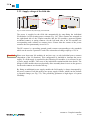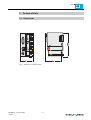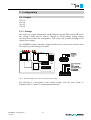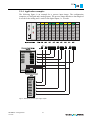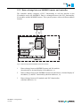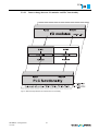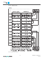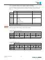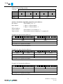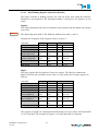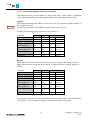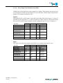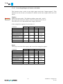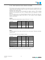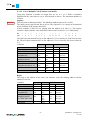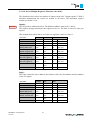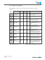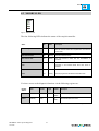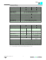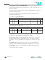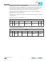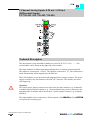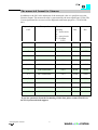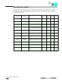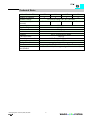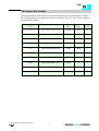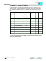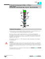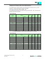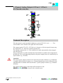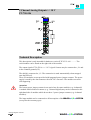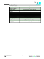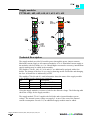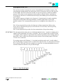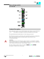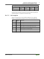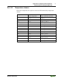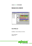
1
Modular I/O System
MODBUS
Manual
Technical description,
installation and
configuration
750-138
Version 2.3.1
ii • General
Copyright ã 1997-2001 by WAGO Kontakttechnik GmbH
All rights reserved.
WAGO Kontakttechnik GmbH
Hansastraße 27
D-32423 Minden
Phone: +49 (0) 571/8 87 – 0
Fax:
+49 (0) 571/8 87 – 1 69
E-Mail: info@wago.com
Web:
http://www.wago.com
Technical Support
Phone: +49 (0) 571/8 87 – 5 55
Fax:
+49 (0) 571/8 87 – 4 30
E-Mail: support@wago.com
Every conceivable measure has been taken to ensure the correctness and completeness of this documentation. However, as errors can never be fully excluded we would appreciate any information or ideas at any time.
We wish to point out that the software and hardware terms as well as the
trademarks of companies used and/or mentioned in the present manual are
generally trademark or patent protected.
Modular I/O System
MODBUS
TABLE OF CONTENTS • iii
TABLE OF CONTENTS
Section 1:
Explanations
Section 2:
System Description MODBUS, Configuration,
Initial Starting, Diagnosis
Section 3:
Digital Inputs
750-400, 750-401, 750-402, 750-403, 750-405, 750-406,
750-410, 750-411, 750-408, 750-409, 750-412, 750-413,
750-414, 750-415
750-404
Section 4:
Digital Outputs
750-501, 750-502, 750-504, 750-516, 750-519
750-506
750-509
750-511
750-512, 750-513, 750-514, 750-517
Section 5:
Analog Inputs
750-452, 750-454, 750-482, 750-484
750-456,
750-461, 750-481
750-462, 750-469
750-465, 750-466, 750-486,
750-467, 750-468, 750-487, 750-488
750-472, 750-474
750-476, 750-478
Section 6:
Analog Outputs
750-550, 750-580
750-552, 750-554, 750-584
750-556
Section 7:
End- and Supply Terminal Blocks
750-600, 750-614, 750-616
750-601, 750-602, 750-609, 750-610, 750-611, 750-612,
750-613, 750-615
750-622
Section 8:
SSI Encoder Interface, Quadrature Encoder Interface
750-630, 750-631
Section 9:
RS232, TTY, RS485
750-650, 750-651, 750-653
Section 0:
Application in Explosive Environments
Modular I/O System
MODBUS
iv • Notes
Modular I/O System
MODBUS
Ensure that the following explanations are observed
To assure a quick installation and start up of the units described in this manual ensure
that the following information and explanations are carefully read and adhered to.
Description of the symbols used
The ATTENTION symbol refers to
a) incorrect handling which can result in damage or destruction to the hardware or
software
b) possible injuries to persons when operating with dangerous peripheral process units.
The FINGER symbol describes routines or gives suggestions for the efficient use of the
unit and optimisation of the software.
ÿþýüûúùýø
The FUNCTION symbol refers to framework conditions which guarantee fault free
operation. Ensure that this information is adhered to.
The QUESTION MARK is intended to clarify terminology.
The BOOK symbol refers to additional literature, manuals data sheets and web
addresses.
MODBUS / Introduction
15.12.99
v
Legal stipulations
This manual including all of its illustrations is copyrighted, deviations from the
copyright stipulations are strictly prohibited. Reproduction, translation as well as
electronic and photographic archiving or changes require the written approval of
WAGO Kontakttechnik GmbH. Non observance will result in claims for damage.
WAGO Kontakttechnik GmbH reserves all rights for changes or amendments which
serve technical progress. All rights for the issuing of patents or the protection of
registered designs are reserved by WAGO Kontakttechnik GmbH. Products of other
suppliers are always referred to without reference to patent rights. For this reason the
existence of such rights cannot be excluded.
The use of the product described in this manual is solely intended for qualified persons
trained in PLC programming, qualified electricians or persons instructed by qualified
electricians who are also familiar with the applicable standards and directives. WAGO
Kontakttechnik GmbH declines all liability for faulty operation and damages to WAGO
products and products from other suppliers resulting from non-observance of the
information contained in this manual.
The components are delivered ex works with a defined hardware and software
configuration for each case of application. Changes are only permitted within the
framework of the possibilities outlined in the manuals. All other changes or
modifications to the hardware or software as well as the use of the components not
conforming with that intended will result in the exclusion from any liability on the part
of WAGO Kontakttechnik GmbH.
Please contact WAGO Kontakttechnik GmbH if a modified hardware or software
configuration is required.
vi
MODBUS / Introduction
15.12.99
List of contents for register 2
1
WAGO-I/O SYSTEM ................................................................. 1
1.1
Components .................................................................................................. 1
1.2
Installation.................................................................................................... 2
1.3
Methods of decentralisation........................................................................ 6
2
MODBUS Coupler/Controller................................................... 9
2.1
Hardware...................................................................................................... 9
2.2
2.2.1
2.2.2
Power supply ................................................................................................ 10
Electronic supply voltage............................................................................... 11
Supply voltage of the field side...................................................................... 12
2.3
Station address ............................................................................................. 13
2.4
Mode switch.................................................................................................. 14
2.5
2.5.1
2.5.2
Fieldbus connection ..................................................................................... 15
RS 485............................................................................................................ 15
RS 232............................................................................................................ 18
3
Technical data ............................................................................. 19
3.1
Dimensions.................................................................................................... 19
3.2
Coupler ......................................................................................................... 20
3.3
Controller ..................................................................................................... 21
4
MODBUS ..................................................................................... 23
5
Configuration .............................................................................. 25
5.1
5.1.1
5.1.1.1
5.1.1.2
5.1.1.3
5.1.1.4
5.1.1.5
5.1.1.6
5.1.1.7
5.1.1.8
5.1.1.9
5.1.2
5.1.3
5.1.4
Coupler .........................................................................................................
Settings...........................................................................................................
Standard settings ............................................................................................
Baud rate setting ............................................................................................
Error detection, length of the character string................................................
End of Frame Time ........................................................................................
ASCII-/RTU mode.........................................................................................
Error Check....................................................................................................
Extended Functions........................................................................................
Watchdog .......................................................................................................
Update Firmware ...........................................................................................
Data exchange between MODBUS master and I/O modules ........................
Addressing the I/O modules...........................................................................
Application examples ....................................................................................
MODBUS / Introduction
15.12.99
vii
25
25
26
26
27
28
28
29
29
30
30
31
32
33
5.2
Controller .....................................................................................................
5.2.1
Settings ..........................................................................................................
5.2.1.1 Standard settings............................................................................................
5.2.1.2 Baud rate setting ............................................................................................
5.2.1.3 Error detection, length of character string .....................................................
5.2.1.4 End of Frame Time........................................................................................
5.2.1.5 ASCII-/RTU mode.........................................................................................
5.2.1.6 Error Check....................................................................................................
5.2.1.7 Extended Functions .......................................................................................
5.2.1.8 Watchdog.......................................................................................................
5.2.2
Data exchange between MODBUS master and controller ............................
5.2.2.1 Data exchange between MODBUS master and I/O modules ........................
5.2.2.2 Data exchange between MODBUS master and PLC functionality ...............
5.2.2.3 Data exchange between I/O modules and PLC functionality ........................
5.2.2.4 Address review ..............................................................................................
5.2.3
Absolute addresses for inputs, outputs and flags...........................................
5.2.4
Addressing the I/O modules ..........................................................................
5.2.5
Application example......................................................................................
5.2.6
Controller operating system...........................................................................
5.3
Common coupler/controller functions.......................................................
5.3.1
Implemented MODBUS functions ................................................................
5.3.1.1 Use of the MODBUS functions.....................................................................
5.3.1.2 Read Coil Status ............................................................................................
5.3.1.3 Read Input Status...........................................................................................
5.3.1.4 Read Holding Register...................................................................................
5.3.1.5 Read Input Register .......................................................................................
5.3.1.6 Force Single Coil ...........................................................................................
5.3.1.7 Preset Single Register....................................................................................
5.3.1.8 Fetch Comm Event Counter ..........................................................................
5.3.1.9 Force Multiple Coils......................................................................................
5.3.1.10 Preset Multiple Registers...............................................................................
5.3.2
Watchdog - Fieldbus failure ..........................................................................
5.3.3
Configuration function ..................................................................................
5.3.4
Firmware information....................................................................................
5.3.5
General registers ............................................................................................
35
35
36
36
37
38
38
39
39
40
41
42
44
45
46
47
49
50
52
53
53
54
55
57
59
60
61
62
63
64
65
66
70
71
72
6
Start up and Diagnosis ............................................................... 73
6.1
Run up and error indications ..................................................................... 73
6.2
MODBUS LED ............................................................................................ 75
6.3
Starting up the controller with WAGO-I/O-PRO .................................... 76
viii
MODBUS / Introduction
15.12.99
7
General Conditions.................................................................... 79
7.1
Transport and storage conditions .............................................................79
7.2
Climatic conditions .....................................................................................79
7.3
Mechanical conditions ................................................................................80
7.4
Class and degree of protection...................................................................81
7.5
Specifications and test results ....................................................................81
7.6
Electromagnetic compatibility...................................................................82
MODBUS / Introduction
15.12.99
ix
x
MODBUS / Introduction
15.12.99
1
WAGO-I/O-SYSTEM
1.1
Components
The WAGO-I/O SYSTEMÿcomprises of various components which allow the creation
of modular and user specific fieldbus nodes for various fieldbusses.
Fig. 1.1: Structure of a fieldbus node with the WAGO-I/O SYSTEM
General:
In all cases a fieldbus node comprises of a fieldbus coupler (1) or a programmable
fieldbus controller (1) as head station, a number of I/O modules (2) and an end module
(3), which forms the end of the system.
In the following description the term Coupler is used for the fieldbus coupler and the
term Controller for the programmable fieldbus controller.
1 – Coupler/Controller:
With its I/O functions the coupler/controller forms the logic operation between the
fieldbus used and the field area. All control tasks necessary for the perfect operation of
the I/O are performed by the coupler/controller. The connection to different fieldbus
systems is made using the corresponding coupler/controller e.g. for PROFIBUS,
INTERBUS, CAN, MODBUS etc. A retrofitting to a different fieldbus system by
changing the coupler is possible.
As opposed to the coupler the controller is fitted with additional PLC functions. This
permits signal pre-processing, which can considerably reduce the data quantity in the
network. In the case of a fieldbus failure the controller can process the control program
independently. Alternatively the controller can guide the node into a defined condition.
Plant modules become independent testable units due to the controller. In the delivered
condition, in other words without the user program, the controller behaves as a coupler.
MODBUS / Introduction
15.12.99
1
The user can program the controller in accordance with international standards for
controller programming, IEC 1131-3 or the corresponding European standard
EN 61131-3, in all five languages, IL, LD, FBD, ST and SFC.
The WAGO-I/O-PRO1 programming system is used for the following functions:
• Programmer setting
• Controller setting
• Loading the program in the controller
• Simulation
• Test and start-up
• Visualisation during operation
• Software documentation
The programming system runs on an IBM compatible PC (for the system requirement
please refer to the WAGO-I/O-PRO user manual).
2 – I/O modules
The input and output of the process data is made at the I/O modules. I/O modules are
available for various tasks in accordance with varying requirements. Available are
digital and analog input and output modules, I/O modules for angle and path
measurement as well as communication modules.
The individual I/O modules are described in detail in the following registers.
3 - End module
The node end module is indispensable. It is always fitted as the last module, to
guarantee the internal node communication. The end module has no I/O function.
_________________________________
1
WAGO-I/O-PRO User manual, English, Order No. 759-120/000-002
2
MODBUS / Introduction
15.12.99
1.2
Installation
All system components can be snapped directly on a carrier rail in accordance with the
European standard EN 50022 (TS 35). Installation is simple and space saving. All
modules have the same shape to minimise the project commitment.
It is not necessary to observe the order of analog and digital modules when engaging on
the rail. The reliable positioning and connection of the coupler/controllers and the
individual I/O modules is made using a tongue and groove system. Due to the
automatic locking the individual components are securely seated on the rail after
installing.
The coupler/controller must be fixed on the
carrier rail with the lateral orange coloured
locking disk.
The coupler/controller is removed by releasing
the locking disk and pulling the release lug
which is also orange coloured.
To fix the coupler/controller apply pressure on
the upper groove of the locking disk using a
screwdriver.
To remove the coupler/controllers release the
locking disk by pressing on the bottom groove.
Fig. 1.2: Coupler/controller, locking disk
It is also possible to release an individual I/O
module from the unit by pulling an unlocking
lug.
Fig. 1.3: Releasing a I/O module
Please note that in this manner the power supply to the field level and the data transfer
is interrupted. Ensure that an interruption of the PE will not result in a condition which
could endanger a person or equipment!
MODBUS / Introduction
15.12.99
3
Conductors with a cross section of from 0.08 to
2.5 mm² can be connected using a CAGE
CLAMP® to achieve a vibration resistant, fast
and maintenance free connection. To actuate the
CAGE CLAMP® enter a screw driver or an
actuation tool in the opening below the
connection. Following this enter the conductor in
the corresponding opening. the conductor is
clamped securely with the removal of the
actuation tool.
Fig. 1.4: Inserting conductor end
The clamping force is automatically adapted to the cross section. The full surface of the
cage clamp pressure is applied against the conductor without damaging it. Conductor
deformation is compensated for and self-loosening is avoided. The transition point
between the conductor and the CAGE CLAMP® is protected against corrosive
influences. The connection can be made quickly and is also maintenance free, saving
the costs for a periodic checking of terminal connections.
The
power
supply
modules
of
the
WAGO-I/O-SYSTEM are, in part, equipped
with a fuse holder. To isolate the following
modules from the power supply the fuse holder
can be removed. For this insert a screwdriver
into one of the slits available on each side and
lift the holder.
Fig. 1.5: Removing the fuse holder
The fuses can be removed from or inserted into
the holder with the fuse holder cover hinged
down. Following this close the cover and push
the fuse holder back into the original position.
Fig. 1.6: Opening the fuse holder
Fig. 1.7: Change fuse
4
MODBUS / Introduction
15.12.99
Do not connect the I/O module to gold spring
contacts in order to avoid soiling and scratches!
Fig. 1.8: Gold contacts
MODBUS / Introduction
15.12.99
5
1.3
Methods of decentralisation
By using the coupler or the controller it is possible to realise various methods for the
decentralisation of control tasks.
Fig. 1.9: Decentralisation methods
Central control using a coupler or a controller (1)
The process methods common to date: All input sensor signals are joined in the coupler
(Slave) and led to the higher ranking controls (Master) via a bus system. The data
generated for signal output in the higher ranking controls reaches the actuators via bus
and nodes. The reaction time of the controls is dependent upon the fieldbus.
This principle can be performed in the same manner using the controller.
Signal pre-processing using controller (2)
Certain control tasks, e.g. impulse generation, delays and counts (e.g. quantity), are
taken care of on site. The logic operations required are processed in the controller. The
bus system only transmits the results of the logic operations as process data to the higher
ranking controls. For signal pre-processing the amount of fieldbus data required is less
than that required for a central connection.
6
MODBUS / Introduction
15.12.99
Decentral control with controller (3)
The on site controller controls an assigned function area, e.g. a machine unit or
components of a transport system. The unit test can be made independently, i.e. without
higher ranking controls.
The higher ranking controls transmit data to the controller via the bus system, e.g. the
operating mode, set point values or the current production program (recipe). The
controller transmits local operating data to the higher ranking controls, such as operating
and control messages, actual values, counter readings etc. The complete linking for
actuator triggering is made in the controller, in other words directly on site. This permits
a fieldbus independent reaction of the controls.
In the case of a fieldbus failure the control program can be independently further
processed and the node put into a defined status.
MODBUS / Introduction
15.12.99
7
8
MODBUS / Introduction
15.12.99
2 MODBUS Coupler/Controller
2.1 Hardware
Fig. 2.1: MODBUS coupler/controller
The illustration above applies both to the MODBUS coupler as well as for the
MODBUS controller.
Each coupler/controller comprises of two enclosure sections:
left:
enclosure for the electronics for bus connection and processing
right:
a fixed installed power supply module as connection and distribution for the
power supply to the electronics in the coupler/controller enclosure, the
assembled I/O modules and the power supply in the field area.
MODBUS / Coupler/controller
15.12.99
9
2.2 Power supply
Fig. 2.2: Power supply
The power supply on the field side is electrically isolated from the electronic supply. In
this manner sensors and actuators can be supplied and fused by a separate voltage
source.
If a non-regulated power supply is used for the 24 V voltage supply of the
coupler/controller electronics, it must be ensured that they are supported by a capacitor
(200 µF per 1 A load current). To this effect a back-up capacitor module1 was developed
for the WAGO-I/O SYSTEM. This module serves for smoothing an unstable 24 V DC
voltage supply, in as much as the specified voltage deviation required cannot be
maintained. Cause for these fluctuations could be a voltage interruption on the primary
side, a secondary side overload or the switching of “non quenched” inductivity and
capacities.
ATTENTION!
Under no circumstances connect a voltage supply other than 24 V DC on the + and –
power supply modules of the coupler/controller. A power supply voltage of max.
230 V AC can only be supplied via the power supply modules 750-609, 750-611 and
750-612!
ATTENTION!
Disconnect the PE lead wires prior to undertaking an insulation test, otherwise this will
result in incorrect results or destruction of the I/O module.
1
Back-up capacitor module, Order No. 288-824
10
MODBUS / Coupler/controller
15.12.99
2.2.1 Electronic supply voltage
Fig. 2.3: Electronic supply voltage
The electronic supply voltage (24 V DC) is adapted using a voltage regulator and led to
the coupler/controller electronics as well as to the internal bus. The electrical isolation
of the external fieldbus system is made via a DC/DC converter and via an optocoupler
in the fieldbus interface.
The internal bus includes the internal communication between the coupler/controller
and the I/O modules as well as the power supply for the I/O modules. The maximum
power supply is 1.65 A. If the sum of the internal power consumption of all I/O modules
exceeds this value it is necessary to fit additional internal system supply modules2.
The control electronics in the I/O modules are supplied by snap-fit mounting the
I/O modules using the internal bus contacts. A reliable contact is assured by gold plated,
self cleaning slide contacts. The removal of a I/O module will cause an interruption of
the connection to the following I/O modules. The coupler/controller localises the
interruption point and sends a corresponding fault message via the red LED ‘I/O ERR’.
ATTENTION!
Removing or inserting the I/O modules with the voltage applied can lead to undefined
conditions. For this reason only undertake work on the I/O modules when isolated from
the power supply!
2
Internal system supply modules, order No. 750-613
MODBUS / Coupler/controller
15.12.99
11
2.2.2 Supply voltage of the field side
Fig. 2.4: Power contact for the power supply to the field side
The power is supplied to the field side automatically by snap-fitting the individual
I/O modules via self-cleaning power contacts (Fig. 2.4). These contacts are arranged on
the right hand side of the coupler/controller and the I/O modules, protected against
accidental contact, as spring contacts. On the left hand side of the I/O modules are
corresponding male contacts as counter pieces. Ensure that the current of the power
contacts does not permanently exceed 10 A.
The PE contact is a preceding ground (earth) contact corresponding to the standards
which can be used as a protective earth. The contact has a leakage capacity of 125 A.
ÿþýüûúùýø Please note that some I/O modules do not have any, or only individual power contacts
(dependent of the I/O function). This configuration is intended to interrupt the power
supply. If a field supply is required for the following I/O modules, it is necessary to use
a power supply module. Take note of the individual terminal/module data sheets! The
design of some modules does not physically allow assembly them in rows as the grooves
for the male contacts are closed at the top.
By fitting an additional power supply module the field supply is always interrupted by
the power contacts. From this point a new power supply is made, which can also include
a potential change (see Fig. 2.2). This possibility guarantees a high degree of system
flexibility.
12
MODBUS / Coupler/controller
15.12.99
2.3 Station address
The station address is set using both coding switches. The settable address is within the
01 and 99 range. The value 00 is reserved for the programming and configuration mode.
The lower coding switch serves for setting the address tens digit, the upper coding
switch for setting the units digit. The address is only read in and saved when switching
on. Changes made during operation have no effect.
The following example shows the setting of address 62:
Fig. 2.5: Coding switch
MODBUS / Coupler/controller
15.12.99
13
2.4 Mode switch
Fig. 2.6: Mode switch
The mode switch is only available in the controller and permits a manual Run/Stopstatus change.
Mode switch setting
Function
From Stop to Run:
Activate program processing
From Run to Stop:
Stop program processing
(Bootstrap:)
To bootstrap the firmware, not required by user
Hardware reset:
Mode switch e.g. push down with screwdriver
All outputs are reset, variables are set to 0 or FALSE or to their initial value.
Flags remain in the same status.
Reset can be made with both Stop as well as Run.
Table 2.1: Mode switch, controller
Stop = Program processing stopped
Run = Program processing running
ATTENTION!
If when changing over the mode switch from ‘Run’ to ‘Stop’ outputs are still
activated, these will remain in this status! Switching off on the software side, e.g.
by initiators is then ineffective because the program will no longer be processed!
(A mode change over is made internally at the end of a program cycle‘.)
14
MODBUS / Coupler/controller
15.12.99
2.5 Fieldbus connection
2.5.1 RS 485
Coupler : 750-312 and 750-315
Controller: 750-812 and 750-815
One transmission medium for the MODBUS is RS485, whereby, 2 or 4 wire can be
used. The following figure shows an example for a 2 wire version:
Fig. 2.7: 2 wire connection
As opposed to the above the 4 wire connection offers the advantage that it can use
simpler repeaters and converter. The following illustration is a corresponding example:
Fig. 2.8: 4 wire connection
MODBUS / Coupler/controller
15.12.99
15
Connect the D-SUB connection plug as follows:
9 pol. D-SUB Signal
Direction
Description
1
-
not used
2
RxD
In
Signal received (4 wire)
3
TxD (RxD)
Out
Signal transmitted (received) (2 wire)
4
DE
Out
Repeater control signal
5
GND
PWR
Signal and supply earth (ground)
6
Vcc
PWR
Supply voltage, +5V (only for external connections)
7
RxD inverted
In
Receive signal with inverted level (4 wire)
8
TxD (RxD) inverted
Out
Send signal with inverted level (receive) (2 wire)
9
-
not used
Table 2.2: Pin assignment for 4 wire connections
The connection point is mechanically lowered so that fitting into a 80 mm deep switch
cabinet is possible following the plug-in connection.
The pin assignment is 2 wire operation conforms with the Profibus assignment. Thus the
Profibus wiring components can be used.
One application possibility is the connection of a Yokogawa Interface. This PCB
supports the MODBUS protocol. The standard setting is the RTU mode (see chapter
MODBUS) and 4 wire connections. The pin assignment is as follows:
9 pol. D-SUB
Signal
25 pol. SUB D
Signal
Colour
1
-
-
-
-
2
RxD
14
SD A
brown
3
TxD (RxD)
16
RD A
red
4
DE
-
-
-
5
GND
25
SG
yellow/black
6
Vcc
-
-
-
7
RxD (inv)
18
SD B
black (brown pair)
8
TxD(RxD) (inv)
19
RD B
black (red pair)
9
-
-
-
-
Table 2.3: Yokogawa interface pin assignment
Switches for RS 485
The setting for 2 or 4 wire connections and switching in or out of the corresponding
matching resistors is made by switches, covered by the enclosure. To access the
switches remove the enclosure from the coupler/controller. A protruding locking device
can be found on the bottom of the unit on the two short sides. Push the two short sides
apart to permit the enclosure to be pushed past the unit metal plate. Simultaneously
press from above on the right hand section of the coupler/controller, which is the supply
side.
16
MODBUS / Coupler/controller
15.12.99
The enclosure prevents unintentional changes of the settings during later operation. If,
however, access to the settings is required in the case of a fault, ensure that the previous
settings are marked on a label.
After changing the settings push the enclosure back onto the coupler/controller. Note
that it may be necessary to lightly push the wide side of the coupler/controllers to the
side when the metal plate does not easily slide into the enclosure. In addition it may be
necessary to push the rotary switches into the cut-outs provided.
The switch on the interface printed circuit board for setting 2 and 4 wire connections or
for the matching resistors can be found in the following illustration:
Fig. 2.9: Interface printed circuit board
For 2 wire connections RxD and TxD are short circuited. By the termination, a series
circuit comprising of 3 resistors is connected to the bus conductor terminations.
Fig. 2.10: Internal matching resistors and interface switches
The standard setting for the supplied coupler/controller is a 2 wire connection and a
switched off matching resistor.
Four wire connections can be terminated as well as the receiver line.
MODBUS / Coupler/controller
15.12.99
17
2.5.2 RS 232
Coupler : 750-314 and 750-316
Controller: 750-814 and 750-816
The MODBUS can also be operated directly on an RS 232 interface. The D-SUB
connection plug is connected in this case as follows:
9-pol. D-SUB Signal
Direction
Description
Signal received
1
-
2
TxD
Out
not used
3
RxD
In
4
-
5
GND
6
-
not used
7
-
not used
8
-
not used
9
-
not used
Signal transmitted
not used
PWR
Signal and supply earth (ground)
Table 2.4: RS 232 plug assignment
The pin assignment permits the use of commercially available 9 pole 1:1 sockets/ plug
lines for direct connection to a PC.
18
MODBUS / Coupler/controller
15.12.99
Configuration Interface
The configuration interface used for the communication with
WAGO-I/O-CHECK or for firmware upload is located behind the cover flap.
Configuration
interface
Fig. X-1: Configuration interface
g01xx06e
The communication cable (750-920) is connected to the 4-pole header.
Warning
The communication cable 750-920 must not be connected or disconnected
while the coupler/controller is powered on!
MODBUS
18a
WAGO-I/O-SYSTEM 750
3 Technical Data
3.1 Dimensions
Fig. 3.1: Dimensions of coupler/controller
MODBUS / Technical data
15.12.99
19
3.2 Coupler
SYSTEM DATA:
750-312
750-314
750-316
99 with repeater
1
about 6,000 (depends on master)
256
Max. number of nodes
Max. number of I/O points
750-315
Shielded Cu cable 2 (4) x 0.25 mm²
Transmission medium
Max. length of bus line
1,200 m (depends on baud rate/on the
Baud rate
150-19,200 bauds
about 5 m
1.2-115.2 kbauds
150-19,200 bauds
RS 485
Type of transmission
1.2-115.2 kbauds
RS 232
Table 3.1: System data, coupler
TECHNICAL DATA:
750-312, 750-314, 750-315, 750-316
64
Max. number of I/O modules
256 (inputs and outputs)
Digital points per node
Analogue points per node
128 (inputs and outputs)
Configuration possibility
DIP switch and decimal coder
via PC or PLC device
1 x D-Sub 9
Bus coupler connection
24 V DC (-15%/+20%)
Voltage supply
350 mA
Internal current consumption
85 mA typ.
Current supply
580 mA max.
Blade / spring contact,
Power jumper contacts
slide contacts, self-cleaning
Voltage power jumper contacts
24 V DC
Current power jumper contacts
10 A DC
1,65 A
Max. current supply at intern.
Slide contacts, 2,5ÿ hart gold-plated
Data contacts
self-cleaning
Polycarbonate, polyamide 6.6
Housing material
Standard marker cards WAGO BR247/278
Marking
Marking cards 8 x 47 mm
CAGE CLAMP, 0.08 mm² - 2.5 mm²
Wire connection
IEC 68-2-6 / IEC 68-2-27
Vibrations-/Schockfestigkeit
any
Fitting position
IP 20
System of protection
500 V system/supply
Insulation
0 °C ... +55 °C
Operating temperature
51 x 65* x 100 (*from upper edge of DIN 35 rail)
Dimensions in mm
Table 3.2: Technical data, coupler
20
MODBUS / Technische Daten
15.12.99
3.3 Controller
SYSTEM DATA:
750-812
Baud rate
750-816
1
about 6,000 (depends on master)
256
Shielded Cu cable 2 (4) x 0.25 mm²
Transmission medium
Max. length of bus line
750-814
99 with repeater
Max. number of nodes
Max. number of I/O points
750-815
1,200 m (depends on baud rate/on the
150-19,200 bauds
about 5 m
1.2-115.2 kbauds
150-19,200 bauds
RS 485
Type of transmission
IEC 1131-3 programming
1.2-115.2 kbauds
RS 232
WAGO-I/O-PRO
IL, LL, FDB, ST, FC
Table 3.3: System data, controller
TECHNICAL DATA:
750-812, 750-814, 750-815, 750-816
64
Max. number of I/O modules
Digital points per node
256 (inputs and outputs)
Analogue points per node
128 (inputs and outputs)
Configuration possibility
With function modules and switches
32 kbytes
Program memory
32 kbytes
Data memory
Residual memory
8 kbytes (retain)
I/O fieldbus area
256 words in input area and 256 words in output area
I/O modules area
256 words for inputs and 256 words for outputs
< 3 ms for 1,000 statements / 256 I/O
Cycle time
1 x D-Sub 9
Bus coupler connection
24 V DC (-15%/+20%)
Voltage supply
350 mA
Internal current consumption
85 mA typ.
Current supply
580 mA max.
Blade / spring contact,
Power jumper contacts
slide contacts, self-cleaning
Voltage power jumper contacts
24 V DC
Current power jumper contacts
10 A DC
1.65 A
Max. current supply at intern.
Slide contacts, 2.5ÿ hart gold-plated
Data contacts
self-cleaning
Polycarbonate, polyamide 6.6
Housing material
Standard marker cards WAGO BR247/278
Marking
Marking cards 8 x 47 mm
CAGE CLAMP, 0.08 mm² - 2.5 mm²
Wire connection
IEC 68-2-6 / IEC 68-2-27
Resistance to shocks/vibrations
any
Fitting position
IP 20
System of protection
500 V system/supply
Insulation
0 °C ... +55 °C
Operating temperature
51 x 65* x 100 (*from upper edge of DIN 35 rail)
Dimensions in mm
Table 3.4: Technical data, controller
MODBUS / Technical data
15.12.99
21
22
MODBUS / Technische Daten
15.12.99
4 MODBUS
MODBUS is a master/slave system. The master is a superimposed control unit, e.g. a
PC or a PLC device. The MODBUS coupler/controller of the WAGO-I/O-SYSTEMS
are slave devices.
Bus conflicts do not occur because only one node is sending. The master makes a query
for communication. This query can be sent to a specific node or to all nodes as a
broadcast message. The nodes receive the query and return a response to the master,
depending on the kind of query.
Fig. 4.1: Example of a MODBUS topology
This bus topology is only valid for the variants with the RS 485 interface. With RS 232
it is only possible to have a peer-to-peer connection.
You will find further information on MODBUS in:
Online information on MODBUS:
http://www.modicon.com/techpubs/toc7.html
MODBUS tools for PC:
http://www.win-tech.com
MODBUS / Description MODBUS
15.12.99
23
24
MODBUS / Description MODBUS
15.12.99
5 Configuration
5.1 Coupler
750-312,
750-314,
750-315,
750-316
5.1.1 Settings
The factory set coupler configuration can be changed using the DIP switches FR and P.
The setting is made prior to start-up. Changes to switch settings during running
operation does not affect the configuration. This is only read in when switching on the
coupler power supply.
The ‘MODBUS coupler/controller’ chapter describes how to remove the enclosure from
the coupler to permit settings to be made.
Fig. 5.1: DIP switch arrangement on CPU printed circuit board, coupler
The following is a description of the coupler settings. Here the term ‘Frame’ is
frequently used. A ‘Frame’ is a data transmission block.
MODBUS / Configuration
15.12.99
25
5.1.1.1 Standard settings
The coupler is supplied with the following standard settings:
Designation
Setting
FR
1
FR
2
FR
3
Baud rate
9600 Bd
off
on
on
Byte Frame
No Parity, 8 Bit
1 Stop Bit
FR
4
FR
5
FR
6
5.1.1.2
off
off
off
End of Frame 3 x Frame Time
Time
Mode
RTU mode
Error Check
to be processed
Extended
Functions
without
Watchdog
switched on
Update
Firmware
normal
operation
P1 P2 P3 P4 P5 P6 P7 P8 Chapt.
5.1.1.3
off
off off
5.1.1.4
on
5.1.1.5
on
5.1.1.6
off
5.1.1.7
off
5.1.1.8
off 5.1.1.9
Table 5.1: Standard settings, coupler
5.1.1.2 Baud rate setting
The baud rate is set using DIP switches FR 1 to FR 3.
Baud rate
Baud rate
FR1
FR2
FR3
750-312/314
750-315/316
150 Bd
38400 Bd
off
off
off
300 Bd
57600 Bd
on
off
off
600 Bd
115200 Bd
off
on
off
1200 Bd
1200 Bd
on
on
off
2400 Bd
2400 Bd
off
off
on
4800 Bd
4800 Bd
on
off
on
9600 Bd
9600 Bd
off
on
on
19200 Bd
19200 Bd
on
on
on
Table 5.2: Baud rates, coupler
The standard setting is 9600 Baud.
26
MODBUS / Configuration
15.12.99
5.1.1.3 Error detection, length of the character string
A parity bit can additionally be transmitted with each byte. Data transfer faults are
detected with the help of the parity bit. A differentiation is made between parity checks
for even parity, odd parity and no parity.
For this the number of set bits (=1) are counted in the transmitted data bytes. For
example, with the transmission of the character string 1100 0101 the number of set bits
is even, namely 4. If the setting of an even parity bit is selected, then in this case it is set
to 0, so that the number of set bits still remains even. Analog to this, the odd parity bit 1
would be selected so that the number of set bits will be odd.
This type of error detection is assured with one error, with several errors under certain
circumstances this may no longer be assured. If the coupler recognises a parity error, the
frame is ignored and a new frame can only be received following a renewed ‘Start of
Frame’.
If the slave receives faulty frames, this will not be replied to. The master detects this
error in that after the preset time (Time-out) no corresponding frame was received.
In the MODBUS coupler 750-312 a parity bit can be attached to each byte. The data
length can be selected for 7 or 8 bit. In addition it is possible to add 1 to 3 stop bits.
Byte Frame
Data length
Stop Bits
FR4
FR5
FR6
No Parity
8
1
off
off
off
Even Parity
8
1
on
off
off
Odd Parity
8
1
off
on
off
No Parity
8
2
on
on
off
No Parity
7
2
off
off
on
Even Parity
7
1
on
off
on
Odd Parity
7
1
off
on
on
No Parity
7
3
on
on
on
Table 5.3: Byte Frame, coupler
The standard setting is no parity, 8 bit data length and 1 stop bit.
During transmission in RTU mode the DIP switch FR6 is ignored, as the format is set to
8 bit in this mode.
MODBUS / Configuration
15.12.99
27
5.1.1.4 End of Frame Time
The end of frame time is the pause time following a frame, which is required to switch
over the repeater in slave. This time must permit gaps during a frame which will not
result in a faulty recognition of the end of frame time. The setting of the
end of frame time is made with DIP switches P1 to P3.
End of Frame Time
P1
P2
P3
3 x Frame Time
off
off
off
100 ms
on
off
off
200 ms
off
on
off
500 ms
on
on
off
1s
off
off
on
1 ms
on
off
on
10 ms
off
on
on
50 ms
on
on
on
Table 5.4: End of Frame Time, coupler
The standard setting is 3 x frame time. The settings 1 ms, 10 ms and 50 ms are only
implemented as from firmware version 2.5 of the MODBUS coupler.
5.1.1.5 ASCII/RTU mode
MODBUS permits two different transmission modes:
ASCII mode:
Advantages:
RTU mode:
Advantages:
Each byte (8 Bit) is sent as a 2 ASCII characters.
Displayable characters are transmitted. The gaps between characters
need not be observed, provided they do not exceed 1 second.
Each byte (8 Bit) comprises of two 4 bit hexadecimal characters.
As only 1 character has to be transmitted for each byte a higher data
throughput is achieved in comparison to the ASCII mode.
The setting is made using DIP switch P4.
Mode
P4
ASCII
off
RTU
on
Table 5.5: ASCII-/RTU mode, coupler
The standard setting is RTU mode.
28
MODBUS / Configuration
15.12.99
5.1.1.6 Error Check
A check sum (CRC) is calculated from the frame to be transmitted in the sender (higher
ranking controls). This check sum is transmitted in the frame to the receiver (coupler).
Once the error check is activated, this check sum is compared with the check sum
calculated in the coupler on the basis of the same instruction. An error is signalled by a
red LED ‘CRC’.
ATTENTION:
Do not set this option during operation!
The error check is set with the DIP switch P5.
Error Check
P5
ignored
off
being processed
on
Table 5.6: Error Check, coupler
The standard setting is the switched on error check.
5.1.1.7 Extended Functions
The register for further internal diagnostic possibilities (extended functions) in the
address space of the coupler are not yet available. For this reason do not change the DIP
switch P6 standard setting (off).
Extended Functions
P6
without
off
available
on
Table 5.7: Extended Functions, coupler
In the standard setting, other diagnostic possibilities are switched off.
MODBUS / Configuration
15.12.99
29
5.1.1.8 Watchdog
The watchdog serves for monitoring the data transfer between the higher ranking
controls and the coupler. If no communication has occurred after a default time, the
node is set into a secured status, i.e. the digital outputs of the node are set to 0 and the
analog outputs are set to the minimum value (e.g. with 4...20 mA to 4 mA).
The watchdog is switched on with DIP switch P7.
Watchdog
P7
switched on
off
switched off
on
Table 5.8: Watchdog, coupler
The standard setting is with the watchdog switched on.
Selection of the watchdog is described in more detail in chapter 5.3.2.
5.1.1.9 Update Firmware
The DIP switch P8 releases the loading of a new firmware. This function has not yet
been implemented, for this reason do not change the standard setting (off) of the switch.
ATTENTION:
Only switch over the DIP switch P8 to update the firmware. Switching over during
operation may lead to a malfunction!
Update Firmware
P8
normal operation
off
Update Firmware
on
Table 5.9: Update firmware, coupler
The standard setting is normal operation.
30
MODBUS / Configuration
15.12.99
5.1.2 Data exchange between MODBUS master and I/O modules
The data exchange between the MODBUS master sand coupler is made by bit or byte
reading and writing.
In the coupler are 4 different types of process data:
•
•
•
•
Input words
Output words
Input bits
Output bits
The addresses of the data words in the process illustration of the inputs and outputs are
shown in the next illustration:
Fig. 5.2: Data exchange between MODBUS master and I/O modules
MODBUS / Configuration
15.12.99
31
Access word for word to the digital input and output modules is made in accordance
with the following table:
Digital inputs/
outputs
8.
7.
6.
5.
4.
3.
2.
1.
16.
15.
14.
13.
12.
11.
10.
9.
Process data word
Bit
15
Bit
14
Bit
13
Bit
12
Bit
11
Bit
10
Bit
9
Bit
8
Bit
7
Bit
6
Bit
5
Bit
4
Bit
3
Bit
2
Bit
1
Bit
0
Byte
High-Byte
Low-Byte
D1
D0
Table 5.10: Allocation of digital inputs/outputs for process data word, coupler
5.1.3 Addressing the I/O modules
•
The arrangement of the I/O modules in a node is optional.
•
The I/O module addressing is based on the attendant coupler.
•
Addressing is organised word for word and starts with the word address ‘0’ both for
the inputs as well as the outputs.
•
The I/O module addressing corresponds to the sequence of their arrangement behind
the coupler. Addressing starts with the bus coupler, which can assign one or more
words per channel. This is followed by the I/O module addresses which can assign
one or two bits per channel. For the number of input and output bits or bytes please
refer to the corresponding I/O module data sheets.
•
Addressing of I/O modules which are assigned to one or two bits per channel is also
made word for word. In other words in each case 16 inputs or outputs are allocated
one word. If less channels are present the remaining bits of the word remain free or
are reserved for extensions.
•
If a node is extended by additional I/O modules for which one or more words are
assigned per channel, the I/O module addresses are displaced by one or two bits per
channel.
Data width ÿ 1 Word / channel
Data width = 1 Bit / channel
Analog input modules
Digital input modules
Analog output modules
Digital output modules
Input modules for thermal elements
Digital output modules with diagnosis (2 Bit / channel)
Input modules for resistance sensors
Power supply modules with fuse holder / diagnosis
Pulse width output modules
Solid State power relay
Interface module
Relay output modules
Up/down counter
I/O modules for angle and path measurement
Table 5.11: I/O module data width
32
MODBUS / Configuration
15.12.99
5.1.4 Application examples
The following figure is an example for a process input image. The configuration
comprises of 10 digital and 8 analog inputs. The process image thus has a data length of
8 words for the analog and 1 word for the digital inputs, i.e. 9 words.
Fig. 5.3: Example for process input image, coupler
MODBUS / Configuration
15.12.99
33
The following configuration comprises of 2 digital and 4 analog outputs. This is an
example for a process output image. It comprises of 4 words for the analog and one
word for the digital outputs.
Fig. 5.4: Example for process output image, coupler
34
MODBUS / Configuration
15.12.99
5.2 Controller
750-812,
750-814,
750-815,
750-816
5.2.1 Settings
As opposed to the MODBUS coupler the factory configuration of the controller change
is not made by DIP switch, but is changed using a PC. The communication between the
controller and PC is described in the ‘Start-up and diagnosis’ chapter.
The controller is set on the software side using the ‘Fieldbus configuration’ function
block of the WAGO-I/O-PRO library. If this module is taken up in the control program,
the setting is made automatically even after changing the controller. The settings are
taken over into the controller parameter block. If the desired values are not already set, a
firmware reset is automatically made in bus operation and the controller restarts with the
selected settings.
If the controller is to be set independent of a machine or plant, a program which only
comprises of the configuration module can be downloaded and started from the
programming system.
Fig. 5.5: Function block for controller setting
The coupler settings are described as follows. Here the term ‘Frame’ is frequently used.
‘Frame’ is a data transfer record.
MODBUS / Configuration
15.12.99
35
5.2.1.1 Standard settings
The controller is delivered with the following standard values:
Input function block
FieldbusConfiguration
Setting
Value
Chapter
BAUDRATE
9600 Bd
6
5.2.1.2
BYTEFRAME
No Parity, 8 Bit
1 Stop Bit
0
5.2.1.3
DATALENGTH
8 Bit
FALSE
5.2.1.3
ENDOFFRAMETIME
3 x Frame Time
0
5.2.1.4
ASCIIRTUMODE
RTU mode
TRUE
5.2.1.5
ERRORCHECKING
being processed
TRUE
5.2.1.6
EXTENDEDFUNCTIONS
without
FALSE
5.2.1.7
NOWATCHDOG
Watchdog switched on
FALSE
5.2.1.8
Table 5.12: Standard settings, controller
5.2.1.2 Baud rate setting
The following baud rates can be set:
Baud rate
Baud rate
BAUDRATE
750-812/814
750-815/816
Value
150 Bd
38400 Bd
0
300 Bd
57600 Bd
1
600 Bd
115200 Bd
2
1200 Bd
1200 Bd
3
2400 Bd
2400 Bd
4
4800 Bd
4800 Bd
5
9600 Bd
9600 Bd
6
19200 Bd
19200 Bd
7
Table 5.13: Baud rates, controller
The standard default setting is 9600 Baud.
36
MODBUS / Configuration
15.12.99
5.2.1.3 Error detection, length of the character string
A parity bit can additionally be transmitted with each byte. Data transfer faults can be
recognised with the help of the parity bit. A differentiation is made between parity
checks for even parity, odd parity and no parity.
For this the number of set bits (=1) are counted in the transmitted data bytes. For
example, during the transmission of the character string 1100 0101 the number of set
bits is even, namely 4. If the setting of an even parity bit is selected, then in this case it
is set to 0, so that the number of set bits still remains even. Analog to this, the odd parity
bit 1 would be selected so that the number of set bits will be odd.
This type of error detection is assured for one error, for several errors under certain
circumstances this error detection may no longer be assured. If the coupler recognises a
parity error, the frame is ignored and a new frame can only be received following a
renewed ‘Start of Frame’.
If the slave receives faulty frames, these will not be replied to. The master detects this
error in that after the preset time (Time-out) no corresponding frame is received.
In the MODBUS coupler 750-812 a parity bit can be attached to each byte. The data
length selected can be 7 or 8 bit. In addition it is possible to add 1 to 3 stop bits.
Byte Frame
Data length
Stop Bits
DATALENGTH
BYTEFRAME
Value
Value
No Parity
8
1
FALSE
0
Even Parity
8
1
FALSE
1
Odd Parity
8
1
FALSE
2
No Parity
8
2
FALSE
3
No Parity
7
2
TRUE
0
Even Parity
7
1
TRUE
1
Odd Parity
7
1
TRUE
2
No Parity
7
3
TRUE
3
Table 5.14: Byte Frame, Controller
The standard setting is no parity, 8 bit data length and 1 stop bit. This setting is ignored
when transferring data in RTU mode, as the format of this mode is set to 8 bit.
MODBUS / Configuration
15.12.99
37
5.2.1.4 End of Frame Time
The end of frame time is the pause time following a frame which is required to switch
over the repeater in slave. This time must permit gaps during a frame without resulting
in a faulty detection of the end of frame time.
The setting of the end of frame time is made with the input ENDOFFRAMETIME.
End of Frame Time
ENDOFFRAMETIME
Value
3 x Frame Time
0
100 ms
1
200 ms
2
500 ms
3
1s
4
1 ms
5
10 ms
6
50 ms
7
Table 5.15: End of Frame Time, Controller
The standard setting is 3 x frame time.
5.2.1.5 ASCII/RTU mode
MODBUS permits two different transmission modes:
ASCII mode:
Advantage:
RTU mode:
Advantage:
Each byte (8 Bit) is sent as 2 ASCII characters.
Displayable characters are transmitted. The gaps between characters
need not be observed, provided they do not exceed 1 second.
Each byte (8 Bit) comprises of two 4 bit hexadecimal characters.
As only 1 character has to be transmitted for each byte a higher data
throughput is achieved in comparison to the ASCII mode.
The setting is made using input ASCIIRTUMODE.
Mode
ASCIIRTUMODE
Value
ASCII
FALSE
RTU
TRUE
Table 5.16: ASCII-/RTU mode, controller
The standard setting is RTU mode.
38
MODBUS / Configuration
15.12.99
5.2.1.6 Error Check
A check sum (CRC) is calculated from the frame to be transmitted in the sender (higher
ranking controls). This check sum is transmitted in the frame to the receiver (controller).
Once the error check is activated, this check sum is compared with the check sum
calculated in the coupler on the basis of the same instruction. An error is signalled by a
red LED ‘CRC’.
The setting is made via the input ERRORCHECKING.
Error Check
ERRORCHECKING
Value
ignored
FALSE
being processed TRUE
Table 5.17: Error Check, controller
Error Check activated is the standard setting.
5.2.1.7 Extended Functions
The registers for further internal diagnostic possibilities (extended functions) in the
address space of the coupler are not yet available. For this reason set the attendant input
EXTENDEDFUNCTIONS to FALSE.
Extended
Functions
EXTENDEDFUNCTIONS
without
FALSE
available
TRUE
Value
Table 5.18: Extended functions, controller
In the standard setting, other diagnosis possibilities are switched off.
MODBUS / Configuration
15.12.99
39
5.2.1.8 Watchdog
The watchdog serves for monitoring the data transfer between the higher ranking
controls and the controller. If no communication occurs after a preset time, the
controller can be run into a secured status.
The watchdog is switched on via the NOWATCHDOG input.
Watchdog
NOWATCHDOG
Value
switched on
FALSE
switched off
TRUE
Table 5.19: Watchdog, controller
Watchdog activated is the standard setting.
The watchdog selection is described is detail in chapter 5.3.2.
40
MODBUS / Configuration
15.12.99
5.2.2 Data exchange between MODBUS master and controller
The controller mainly comprises of PLC functionality as well the interface to the
I/O modules and to the MODBUS. Data is exchanged between the PLC functionality,
I/O modules and the MODBUS master. This system operates with two different address
formats.
Fig. 5.6: Data exchange between MODBUS master and controller
1
Data exchange between MODBUS master and I/O modules
(hexadecimal or decimal display of the addresses, x)
2
Data exchange between the MODBUS master (hexadecimal or decimal display of
the address, x) and PLC functionality (absolute addresses, %)
3
Data exchange between I/O modules and PLC functionality
(absolute addresses, %)
MODBUS / Configuration
15.12.99
41
5.2.2.1 Data exchange between MODBUS master and I/O modules
The data exchange between the MODBUS master and the I/O modules is made by
reading and writing in bits or bytes.
The controller handles four different types of process data:
•
•
•
•
Input words
Output words
Input bits
Output bits
The following figure shows the data word addresses in the process illustration of the
inputs and outputs:
Fig. 5.7: Data exchange between the MODBUS master and I/O modules
42
MODBUS / Configuration
15.12.99
The word for word access to the digital input and output modules is made in accordance
with the following table:
Digital inputs/
outputs
16.
15.
14.
13.
12.
11.
10.
9.
8.
7.
6.
5.
4.
3.
2.
1.
Process data word
Bit
15
Bit
14
Bit
13
Bit
12
Bit
11
Bit
10
Bit
9
Bit
8
Bit
7
Bit
6
Bit
5
Bit
4
Bit
3
Bit
2
Bit
1
Bit
0
Byte
High-Byte
Low-Byte
D1
D0
Table 5.20: Allocation of digital inputs/outputs to process data word, controller
ÿþýüûúùýø
Common access of MODBUS master and PLC functionality to outputs
The process illustration of outputs is described both by the MODBUS master as well as
by the PLC functionality, so that the I/O module outputs can be set or reset from both
sides. In the case of simultaneity no priority exists. Design the user programs of the
MODBUS master and the PLC functionality such that conflicting instructions for
simultaneous setting or resetting of outputs is excluded. Applicable in all cases is that
the individual instruction of the process illustration processed last will be written over.
MODBUS / Configuration
15.12.99
43
5.2.2.2 Data exchange between MODBUS master and PLC functionality
The fieldbus data in the MODBUS master and in the PLC functionality have different
address formats. The addresses of the MODBUS master are displayed hexadecimal or
decimal. The PLC functionality uses absolute addresses.
Fig. 5.8: Data exchange between MODBUS master and PLC functionality
44
MODBUS / Configuration
15.12.99
5.2.2.3
Data exchange between I/O modules and PLC functionality
Fig. 5.9: Data exchange between I/O modules and PLC functionality
MODBUS / Configuration
15.12.99
45
5.2.2.4 Address review
Fig. 5.10: Address review, controller
46
MODBUS / Configuration
15.12.99
5.2.3 Absolute addresses for inputs, outputs and flags
The direct display of individual memory cells (absolute addresses) in accordance with
IEC 1131-3 is made using special character strings in accordance with the following
table:
Position
Character
Designation
Comments
1
%
Starts absolute address
2
I
Input
Q
Output
M
Flag
X*
Single bit
B
Byte (8 Bits)
W
Word (16 Bits)
D
Double word (32 Bits)
3
Data width
Address
4
* The character ‘X’ for bits can be deleted
Table 5.21: Absolute addresses
Enter the absolute address character strings without blanks!
Address range for I/O module data:
Data width
Address
Bit
0.0 ... 0.15
1.0 ... 1.15
Byte
0
2
Word
1
3
0
.....
.....
1
DWord
254.0 ... 254.15
.....
508
.....
0
255.0 ... 255.15
509
510
254
511
255
.....
127
Table 5.22: Address range for the I/O module data
Fieldbus data address range:
Data width
Bit
Byte
Word
DWord
Address
256.0 ... 256.15
512
257.0 ... 257.15
513
514
256
515
257
128
15.12.99
.....
.....
.....
.....
Table 5.23: Address range for fieldbus data
MODBUS / Configuration
.....
47
510.0 ... 510.15
511.0 ... 511.15
1020
1022
1021
510
1023
511
255
Address range for flags (retain):
Data width
Address
Bit
0.0 ... 0.15
Byte
0
Word
1.0 ... 1.15
1
2
0
DWord
.....
3
1
0
.....
4094.0 ... 4094.15
.....
8188
.....
4095.0 ... 4095.15
8189
8190
4094
8191
4095
.....
2047
Table 5.24: Address range for flags
Address calculation (depending upon the word address):
Bit address:
Word address .0 to .15
Byte address:
1. Byte: 2 x Word address
2. Byte: 2 x Word address + 1
DWord address:
Lower section:
Word address (even numbers) / 2
Upper section:
Word address (uneven numbers) / 2, rounded off
Example for input absolute addresses:
%IX14. 0 1 2 3 4 5 6 7 8
%IB28
9 10 11 12 13 14 15 %I15.* 0 1 2 3 4 5 6 7 8
%IB29
9 10 11 12 13 14 15
%IB30
%IW14
%IB31
%IW15
%IDW7
* The character ‘X’ for single bits can be deleted
Table 5.25: Example for input absolute addresses
Example for output absolute addresses:
%QX5. 0 1 2 3 4 5 6 7 8
%QB10
9 10 11 12 13 14 15 %Q6.* 0 1 2 3 4 5 6 7 8
%QB11
%QB12
9 10 11 12 13 14 15
%QB13
%QW5
%QW6
%QDW2 (upper section)
QDW3 (lower section)
* The character ‘X’ for single bits can be deleted
Table 5.26: Example for output absolute addresses
Example for flag absolute addresses:
%MX11. 0 1 2 3 4 5 6 7 8
%MB22
9 10 11 12 13 14 15 %M12.* 0 1 2 3 4 5 6 7 8
%MB23
%MB24
9 10 11 12 13 14 15
%MB25
%MW11
%MW12
%MDW5 (upper section)
%MDW6 (lower section)
* The character ‘X’ for single bits can be deleted
Table 5.27: Example for flag absolute addresses
48
MODBUS / Configuration
15.12.99
5.2.4 Addressing the I/O modules
•
The arrangement of the I/O modules in a node is optional.
•
Addressing of the I/O modules relates to the attendant controller.
•
Addressing is organised word for word and starts both for inputs as well as outputs
with word address ‘0’.
•
The I/O module addressing corresponds to the arrangement order behind the
controller. Addressing starts with the I/O module, which occupy one or more words
per channel. The I/O module addresses which occupy one or two bits per channel
then follow. For the number of input and output bits or bytes please refer to the
corresponding I/O module data sheets.
•
Addressing of the I/O modules which occupy one or two bits per channel is also
made word for word. 16 inputs or outputs each are arranged in one word. If less
channels are available the remaining bits of the word remain free or are reserved for
extensions.
•
If a node is extended by additional I/O modules for which one or more words are
assigned per channel, the I/O module addresses are displayed accordingly by one or
two bits per channel.
Data width ÿ 1 word / channel
Data width = 1 Bit / channel
Analog input modules
Digital input modules
Analog output modules
Digital output modules
Input modules for thermal elements
Digital output modules with diagnosis (2 Bit / channel)
Input modules for resistance sensors
Power supply module with fuse holder / diagnosis
Pulse width output modules
Solid State power relay
Interface modules
Relay output modules
Up/down counter
I/O modules for angle and path measurement
Table 5.28: Data width of I/O modules
MODBUS / Configuration
15.12.99
49
5.2.5 Application example
The following figure is an example of a process input image. The configuration
comprises of 10 digital and 8 analog inputs. The process image thus has a data length of
8 words for the analog and 1 word for the digital inputs, i.e. 9 words in total.
Fig. 5.11: Example for process input image, controller
50
MODBUS / Configuration
15.12.99
The following example for the process output image comprises of 2 digital and 4 analog
outputs. It comprises of 4 words for the analog and one word for the digital outputs.
Fig. 5.12: Example for process output image, controller
MODBUS / Configuration
15.12.99
51
5.2.6 Controller operating system
Fig. 5.13: Operating system, controller
52
MODBUS / Configuration
15.12.99
5.3 Common coupler/controller functions
5.3.1 Implemented MODBUS functions
The following table shows the functions which support both the MODBUS coupler as
well as the MODBUS controller:
Function
code
Function
Description
0x01
Read Coil Status
Read input bits and output bits as an octet string.
0x02
Read Input Status
Read input bit as an octet string.
0x03
Read Holding Registers Read number of input words.
0x04
Read Input Registers
Read number of input words.
0x05
Force Single Coil
Write output bit.
0x06
Preset Single Register
Writes a value in an output word.
0x0B
Fetch Comm Event Ctr
Read status word and event counter.
0x0F
Force Multiple Coils
Writes a number of output bits.
0x10
Preset Multiple Regs
Writes a number of output words.
Table 5.29: Implemented functions
MODBUS / Configuration
15.12.99
53
Functions are
identical
Functions are
identical
5.3.1.1 Use of the MODBUS functions
The graphical review shows the MODBUS functions which have access to process
illustration data.
Fig. 5.14: Review of MODBUS functions, e.g. with coupler
It is to be recommended to access the analog signals with register functions ➀ and
binary signals with coil functions ➁. If access is also required to reading and writing
binary signals with register functions ➂, the addresses are displayed as soon as a further
analog modules are fitted.
54
MODBUS / Configuration
15.12.99
5.3.1.2 Read Coil Status (function code 0x01):
This function reads the status of the input and output bits (coils) in slave, whereby
broadcast is not supported. With coupler/controller the number of I/O points is limited
to 256.
ÿþýüûúùýø
Inquiry:
The Inquiry determines the starting address and the number of bits to be read.
The first point is addressed with 0. With Modicon the addressing starts with 1 (0x01).
The following table shows an example for an inquiry, with which the bits 0 to 7 of the
slaves 11 are to be read:
Field name
Example
RTU
ASCII
Start of frame
-
t1-t2-t3
”:”
Slave address
0x0B
0x0B
”0B”
0x30, 0x42
Function code
0x01
0x01
”01”
0x30, 0x31
Starting address high
0x00
0x00
”00”
0x30, 0x30
Starting address low
0x00
0x00
”00”
0x30, 0x30
Number of points high
0x00
0x00
”00”
0x30, 0x30
Number of points low
0x08
0x08
”08”
0x30, 0x38
Error Check (LRC / CRC)
-
0x3D
0x66
”EC”
0x45, 0x43
t1-t2-t3
-
0xD, 0xA
End of frame
0x3a
Table 5.30: Inquiry example, Read Coil Status
Reply:
The current values of the interrogated bits are packed in the data field. A 1 corresponds
to the ON status and a 0 to the OFF status. The lowest value bit of the first data byte
contains the first bit of the inquiry. The others follow in an ascending order. If the
number of inputs are not a multiple of 8, the remaining bits of the last data byte are
filled with zeroes. If the number of bits interrogated exceed the number of inputs or
outputs present in the node, the remaining input bits are set to zero and the outputs
contain the last valid value.
Field name
Example
RTU
Start of frame
-
t1-t2-t3
”:”
0x3A
Slave address
0x0B
0x0B
”0B”
0x30, 0x42
Function code
0x01
0x01
”01”
0x30, 0x31
Byte Count
0x01
0x01
”01”
0x30, 0x31
Data (point 8...0)
0x12
0x12
”12”
0x31, 0x32
Error Check (LRC / CRC)
-
0xD2
0x5D
”E1”
0x45, 0x31
End of frame
-
t1-t2-t3
-
0xD, 0xA
Table 5.31: Reply example, Read Coil Status
MODBUS / Configuration
15.12.99
55
ASCII
The status of the inputs 7 to 0 is shown as byte value 0x12 or binary 0001 0010. Input 7
is the bit having the highest valency of this byte and input 0 the lowest value.
The assignment is thus made from 7 to 0 with OFF-OFF-OFF-ON-OFF-Off-ON-OFF.
Bit:
0
0
0
1
0
0
1
0
Coil:
7
6
5
4
3
2
1
0
56
MODBUS / Configuration
15.12.99
5.3.1.3 Read Input Status (function code 0x02):
This function reads the input bits in the slave, whereby broadcast is not supported. With
the coupler/controller the number of points is limited to 256.
ÿþýüûúùýø
Inquiry:
The inquiry determines the starting address and the number of bits to be read.
The first point is addressed with 0. With Modicon addressing starts with 1 (0x01).
The following table shows an example of an inquiry with which the bits 0 to 7 of the
slaves 11 are to be read:
Field name
Example
RTU
ASCII
Start of frame
-
t1-t2-t3
”:”
Slave address
0x0B
0x0B
”0B”
0x30, 0x42
Function code
0x02
0x02
”02”
0x30, 0x32
Starting address high
0x00
0x00
”00”
0x30, 0x30
Starting address low
0x00
0x00
”00”
0x30, 0x30
Number of points high
0x00
0x00
”00”
0x30, 0x30
Number of points low
0x08
0x08
”08”
0x30, 0x38
Error Check (LRC / CRC)
-
0x79
0x66
”EC”
0x45, 0x42
t1-t2-t3
-
0xD, 0xA
End of frame
0x3a
Table 5.32: Example inquiry, Read Input Status
Reply:
The current value of the inquired bit is packed into the data field. A 1 corresponds to
the ON status and a 0 the OFF status. The lowest value bit of the first data byte contains
the first bit of the inquiry. The other follow in an ascending order. If the number of
inputs are not a multiple of 8, the remaining bits of the last data byte are filled with
zeroes. If the number of bits interrogated exceed the number of inputs present in the
node, the remaining input bits are set to zero.
Field name
Example
RTU
ASCII
Start of frame
-
t1-t2-t3
”:”
Slave address
0x0B
0x0B
”0B”
0x30, 0x42
Function code
0x02
0x02
”02”
0x30, 0x32
Byte Count
0x01
0x01
”01”
0x30, 0x31
Data (point 8...0)
0x12
0x12
”12”
0x31, 0x32
Error Check (LRC / CRC)
-
0x22
0x5D
”E0”
0x45, 0x30
End of frame
-
t1-t2-t3
-
0xD, 0xA
Table 5.33: Example reply, Read Input Status
MODBUS / Configuration
15.12.99
57
0x3A
The status of the inputs 7 to 0 is shown as a byte value 0x12 or binary 0001 0010. Input
7 is the bit having the highest valency of this byte and input 0 the lowest value.
The assignment is thus made from 7 to 0 with OFF-OFF-OFF-ON-OFF-Off-ON-OFF.
Bit:
0
0
0
1
0
0
1
0
Coil:
7
6
5
4
3
2
1
0
58
MODBUS / Configuration
15.12.99
5.3.1.4 Read Holding Register (function code 0x03)
The binary contents of holding registers are read out in the slave using this function.
Broadcast is not supported. The maximum number is limited to 128 registers in one
frame.
Inquiry:
The inquiry determines the start word address (start register) and the number the register
to be read.
ÿþýüûúùýø
The addressing starts with 0. The Modicon address starts with 1 (0x01).
Example for an inquiry of the registers 0 and 1 of slave 11:
Field name
Example
RTU
ASCII
Start of frame
-
t1-t2-t3
”:”
Slave address
0x0B
0x0B
”0B”
0x30, 0x42
Function code
0x03
0x03
”03”
0x30, 0x33
Starting address high
0x00
0x00
”00”
0x30, 0x30
Starting address low
0x00
0x00
”00”
0x30, 0x30
Number of points high
0x00
0x00
”00”
0x30, 0x30
Number of points low
0x02
0x02
”02”
0x30, 0x32
Error Check (LRC / CRC)
-
0xC4
0xA1
”F0”
0x46, 0x30
t1-t2-t3
-
0xD, 0xA
End of frame
0x3a
Table 5.34: Example inquiry, Read Holding Register
Reply:
The reply register data is packed as 2 bytes per register. The first byte contains the
higher value bits, the second the lower values. A reply to the above inquiry appears as
follows:
Field name
Example
RTU
ASCII
Start of frame
-
t1-t2-t3
”:”
0x3A
Slave address
0x0B
0x0B
”0B”
0x30, 0x42
Function code
0x03
0x03
”03”
0x30, 0x33
Byte Count
0x04
0x04
”04”
0x30, 0x34
Data Hi (Register 0)
0x3F
0x3F
”3F”
0x33, 0x46
Data Lo (Register 0)
0xFB
0xFB
”FB”
0x46, 0x42
Data Hi (Register 1)
0x00
0x00
”00”
0x30, 0x30
Data Lo (Register 1)
0x00
0x00
”00”
0x30, 0x30
Error Check (LRC / CRC)
-
0x2D
0x61
”B4”
0x42, 0x34
End of frame
-
t1-t2-t3
-
0xD, 0xA
Table 5.35: Example reply, Read Holding Register
The contents of register 0 is displayed hexadecimal by two byte values: 0x3F and 0xFB
or 16379 decimal. The contents of register 1 are 0x00 and 0x00 or 0 decimal.
MODBUS / Configuration
15.12.99
59
5.3.1.5 Read Input Register (Function code 0x04)
This function serves to read a number of input words (also ”input register”). Broadcast
is not supported and the maximum number is limited to 128 registers in one frame.
ÿþýüûúùýø
Inquiry:
The inquiry determines the address of the start word (start register) and the number of
the register to be read.
Addressing starts with 0. The Modicon address starts with 1 (0x01).
Example for an inquiry of the registers 0 and 1 ofslave 11:
Field name
Example
RTU
ASCII
Start of frame
-
t1-t2-t3
”:”
Slave address
0x0B
0x0B
”0B”
0x30, 0x42
Function code
0x04
0x03
”03”
0x30, 0x33
Starting address high
0x00
0x00
”00”
0x30, 0x30
Starting address low
0x00
0x00
”00”
0x30, 0x30
Number of points high
0x00
0x00
”00”
0x30, 0x30
Number of points low
0x02
0x02
”02”
0x30, 0x32
Error Check (LRC / CRC)
-
0xC4
0xA1
”F0”
0x46, 0x30
t1-t2-t3
-
0xD, 0xA
End of frame
0x3a
Table 5.36: Example enquiry, Read Input Register
Replay:
The register data of the answer is packed as 2 bytes per register. The first byte has the
higher value bits, the second the lower values. A reply to the above inquiry appears as
follows:
Field name
Example
RTU
ASCII
Start of frame
-
t1-t2-t3
”:”
0x3A
Slave address
0x0B
0x0B
”0B”
0x30, 0x42
Function code
0x04
0x03
”03”
0x30, 0x33
Byte Count
0x04
0x04
”04”
0x30, 0x34
Data Hi (Register 0)
0x3F
0x3F
”3F”
0x33, 0x46
Data Lo (Register 0)
0xFB
0xFB
”FB”
0x46, 0x42
Data Hi (Register 1)
0x00
0x00
”00”
0x30, 0x30
Data Lo (Register 1)
0x00
0x00
”00”
0x30, 0x30
Error Check (LRC / CRC)
-
0x2D
0x61
”B4”
0x42, 0x34
End of frame
-
t1-t2-t3
-
0xD, 0xA
Table 5.37: Example reply, Read Input Register
The contents of register 0 are shown hexadecimal by two byte values: 0x3F and 0xFB or
16379 decimal. The contents of register 1 are 0x00 and 0x00 or 0 decimal.
60
MODBUS / Configuration
15.12.99
5.3.1.6 Force Single Coil (Function code 0x05):
With the aid of this function a single output bit is written. This function can also be sent
as a broadcast, in which case the same bit is set in all slaves. With coupler/controller the
number of I/O points is limited to 256.
Inquiry:
The required ON or OFF status is specified in the data field of the inquiry. A value of
0xFF00 sets the output bit to 1, a value of 0x00 on 0. Other values are not specified and
have no effect on the output condition. In this example the bit 0 is set to 1 in slave 11:
Field name
Example
RTU
ASCII
Start of frame
-
t1-t2-t3
”:”
Slave address
0x0B
0x0B
”0B”
0x30, 0x42
Function code
0x05
0x05
”05”
0x30, 0x35
Coil address high
0x00
0x00
”00”
0x30, 0x30
Coil address low
0x00
0x00
”00”
0x30, 0x30
Force data high
0xFF
0xFF
”FF”
0x46, 0x46
Force data low
0x00
0x00
”00”
0x30, 0x30
Error Check (LRC / CRC)
-
0x8C
0x90
”F1”
0x46, 0x31
t1-t2-t3
-
0xD, 0xA
End of frame
0x3a
Table 5.38: Example inquiry, Force Single Coil
Reply:
The reply is an echo of the inquiry and will be or is returned when the bit is set.
Field name
Example
RTU
Start of frame
-
t1-t2-t3
”:”
0x3a
Slave address
0x0B
0x0B
”0B”
0x30, 0x42
Function code
0x05
0x05
”05”
0x30, 0x35
Coil address high
0x00
0x00
”00”
0x30, 0x30
Coil address low
0x00
0x00
”00”
0x30, 0x30
Force data high
0xFF
0xFF
”FF”
0x46, 0x46
Force data low
0x00
0x00
”00”
0x30, 0x30
Error Check (LRC / CRC)
-
0x8C
0x90
”F1”
0x46, 0x31
t1-t2-t3
-
0xD, 0xA
End of frame
Table 5.39: Example reply, Force Single Coil
MODBUS / Configuration
15.12.99
61
ASCII
5.3.1.7 Preset Single Register (Function code 0x06):
This function writes a value in one single output word (also ”Output register”). This
function can also be sent as a broadcast, in which case the same output word is set in all
slaves.
ÿþýüûúùýø
Inquiry:
Addressing starts with 0. The Modicon address starts with 1 (0x01).
The inquiry determines the address of the first output word to be set.
The value to be set is determined in the inquiry data field.
In the example the register 0 is set in slave 11.
Field name
Example
RTU
ASCII
Start of frame
-
t1-t2-t3
”:”
Slave address
0x0B
0x0B
”0B”
0x30, 0x42
Function code
0x06
0x06
”06”
0x30, 0x36
Register address high
0x00
0x00
”00”
0x30, 0x30
Register address low
0x00
0x00
”00”
0x30, 0x30
Preset data high
0x12
0x12
”12”
0x31, 0x32
Preset data low
0x34
0x34
”34”
0x33, 0x34
Error Check (LRC / CRC)
-
0x8C
0x17
”A9”
0x41, 0x39
t1-t2-t3
-
0xD, 0xA
End of frame
0x3a
Table 5.40: Example inquiry, Preset Single Register
Reply:
The reply is an echo of the inquiry and is sent after setting the register.
Field name
Example
RTU
ASCII
Start of frame
-
t1-t2-t3
”:”
Slave address
0x0B
0x0B
”0B”
0x30, 0x42
Function code
0x06
0x06
”06”
0x30, 0x36
Register address high
0x00
0x00
”00”
0x30, 0x30
Register address low
0x00
0x00
”00”
0x30, 0x30
Preset data high
0x12
0x12
”12”
0x31, 0x32
Preset data low
0x34
0x34
”34”
0x33, 0x34
Error Check (LRC / CRC)
-
0x8C
0x17
”A9”
0x41, 0x39
t1-t2-t3
-
0xD, 0xA
End of frame
0x3a
Table 5.41: Example reply, Preset Single Register
62
MODBUS / Configuration
15.12.99
5.3.1.8 Fetch Comm Event Counter (Function code 0x0B):
This function returns a status word and an event counter from the communication event
counter of the slave. With this counter the master can determine whether the slave has
treated the slave without a fault.
Following each successful news processing the counter counts up. This counting
process is not performed in the case of exception replies, poll commands or counter
inquiries.
The event counter can be reset using the diagnosis function (Code 0x08), the restart subfunction communications option (Code 0x01) or clear counters and the diagnosis
register (Code 0x0A).
Inquiry:
In the example the communication counter of the slave 11 is read:
Field name
Example
RTU
Start of frame
-
t1-t2-t3
”:”
0x3a
Slave address
0x0B
0x0B
”0B”
0x30, 0x42
Function code
0x0B
0x0B
”0B”
0x30, 0x42
Error Check (LRC / CRC)
-
0x47
0x47
”EA”
0x45, 0x41
t1-t2-t3
-
0xD, 0xA
End of frame
ASCII
Table 5.42: Example inquiry, Fetch Comm Event Counter
Reply:
The reply contains a 2 byte status word and a 2 byte event counter. The status word only
contains zeroes.
The following table shows an example of a reply:
Field name
Example
RTU
ASCII
Start of frame
-
t1-t2-t3
”:”
0x3a
Slave address
0x0B
0x0B
”0B”
0x30, 0x42
Function code
0x0B
0x0B
”0B”
0x30, 0x42
Status high
0x00
0x00
”00”
0x30, 0x30
Status low
0x00
0x00
”00”
0x31, 0x33
Event count high
0x00
0x00
”00”
0x30, 0x30
Event count low
0x03
0x03
”03”
0x30, 0x33
Error Check (LRC / CRC)
-
0xE4
0xA0
”E7”
0x45, 0x37
t1-t2-t3
-
0xD, 0xA
End of frame
Table 5.43: Example reply, Fetch Comm Event Counter
The event counter shows that 3 (0x03) events were counted.
MODBUS / Configuration
15.12.99
63
5.3.1.9 Force Multiple Coils (Function code 0x0F):
ÿþýüûúùýø
Using this function a number of output bits are set to 1 or 0. With a broadcast
transmission the same bits are set in all activated on slaves. The maximum number is
256 bits.
Inquiry:
The first point is addressed with 0. The Modicon address starts with 1 (0x01).
The inquiry news specifies the bits to be set. The requested 1 or 0 states are determined
by the contents of the inquiry data field.
In this example 16 bits are set, starting with the address 0 in slave 11. The inquiry
contains 2 bytes with the value 0xA5F0 in other words 1010 0101 1111 0000 binary.
Bit:
1
0
1
0
0
1
0
1
1
1
1
1
0
0
0
0
Coil:
7
6
5
4
3
2
1
0
15
14
13
12
11
10
9
8
The first byte transmits the 0xA5 to the addresses 7 to 0, whereby 0 is the lowest value
bit. The next byte transmits 0xF0 to the addresses 15 to 8, whereby the lowest value bit
is 8.
Field name
Example
RTU
ASCII
Start of frame
-
t1-t2-t3
”:”
Slave address
0x0B
0x0B
”0B”
0x30, 0x42
Function code
0x0F
0x0F
”0F”
0x30, 0x46
Coil address high
0x00
0x00
”00”
0x30, 0x30
Coil address low
0x00
0x00
”00”
0x30, 0x30
Quantity of coils high
0x00
0x00
”00”
0x30, 0x30
Quantity of coils low
0x10
0x10
”10”
0x31, 0x30
Byte Counter
0x02
0x02
”02”
0x30, 0x32
Force data high (coils 7 ... 0)
0xA5
0xA5
”A5”
0x41, 0x35
Force data low (coils 15 ... 8)
0xF0
0xF0
”F0”
0x46, 0x30
Error Check (LRC / CRC)
-
0xE7
0x94
”3F”
0x33, 0x46
t1-t2-t3
-
0xD, 0xA
End of frame
0x3a
Table 5.44: Example inquiry, Force Multiple Coils
Reply:
The reply is the address of the slave, the function code, the starting address and the
number of set bits.
Fieldname
Example
RTU
Start of frame
-
t1-t2-t3
”:”
0x3a
Slave address
0x0B
0x0B
”0B”
0x30, 0x42
Function code
0x0F
0x0F
”0F”
0x30, 0x46
Coil address high
0x00
0x00
”00”
0x30, 0x30
Coil address low
0x00
0x00
”00”
0x30, 0x30
Quantity of coils high
0x00
0x00
”00”
0x30, 0x30
Quantity of coils low
0x10
0x10
”10”
0x31, 0x30
Error Check (LRC / CRC)
-
0x54
0xAD
”D6”
0x44, 0x36
t1-t2-t3
-
0xD, 0xA
End of frame
ASCII
Table 5.45: Example reply, Force Multiple Coils
64
MODBUS / Configuration
15.12.99
5.3.1.10 Preset Multiple Registers (Function code 0x10):
This function writes values in a number of output words (also ”Output register”). With a
broadcast transmission the values are written in all slaves. The maximum register
number per frame is 128.
ÿþýüûúùýø
Inquiry:
The first point is addressed with 0. The Modicon address starts with 1 (0x01).
The inquiry message determines the registers to be set. The data is sent as 2 bytes per
register.
The example shows how data is set in the two registers 0 and 1 in slave 11:
Field name
Example
RTU
ASCII
Start of frame
-
t1-t2-t3
”:”
Slave address
0x0B
0x0B
”0B”
0x30, 0x42
Function code
0x10
0x10
”10”
0x31, 0x30
Starting address high
0x00
0x00
”00”
0x30, 0x30
Starting address low
0x00
0x00
”00”
0x30, 0x30
Number of register high
0x00
0x00
”00”
0x30, 0x30
Number of register low
0x02
0x02
”02”
0x30, 0x32
Byte Counter
0x04
0x04
”04”
0x30, 0x34
Data high (register 0)
0x12
0x12
”12”
0x31, 0x32
Data low (register 0)
0x34
0x34
”34”
0x33, 0x34
Data high (register 1)
0x56
0x56
”56”
0x35, 0x36
Data low (register 1)
0x78
0x78
”78”
0x37, 0x38
Error Check (LRC / CRC)
-
0xA9
0x43
”CB”
0x43, 0x42
t1-t2-t3
-
0xD, 0xA
End of frame
0x3a
Table 5.46: Example inquiry, Preset Multiple Registers
Reply:
The reply returns the slave address, the function code, the start address and the number
of the set register.
Field name
Example
RTU
ASCII
Start of frame
-
t1-t2-t3
”:”
Slave address
0x0B
0x0B
”0B”
0x30, 0x42
Function code
0x10
0x10
”10”
0x31, 0x30
Starting address high
0x00
0x00
”00”
0x30, 0x30
Starting address low
0x00
0x00
”00”
0x30, 0x30
Number of register high
0x00
0x00
”00”
0x30, 0x30
Number of register low
0x02
0x02
”02”
0x30, 0x32
Error Check (LRC / CRC)
-
0x41
0x62
”E3”
0x45, 0x33
t1-t2-t3
-
0xD, 0xA
End of frame
Table 5.47: Example reply, Preset Multiple Registers
MODBUS / Configuration
15.12.99
65
0x3a
5.3.2 Watchdog - Fieldbus failure
ÿþýüûúùýø
The watchdog serves for monitoring the data transfer between the higher ranking
controls and coupler/controller. For this the higher ranking controls cyclically actuate a
time function (Time-out) in the coupler/controller. In the case of fault free
communication this time cannot reach its end value, because prior to this it is restarted
again and again. If this time has elapsed a fieldbus failure has occurred.
The watchdog must be switched on so that it can be activated (see ‘coupler/settings’ or
‘Controller/settings’).
In the coupler/controller special registers are present for the selection and status inquiry
of the watchdog by the higher ranking controls (Register addresses 0x1000 to 0x1008).
After switching on the supply voltage the watchdog is not yet activated. First lay down
the time-out value (Register 0x1000). The watchdog can be activated by writing a
function code in the mask register (0x1001), which is unequal 0. A second activation
possibility is to write a value in the toggle register (0x1003) deviating from 0.
Reading the minimum trigger time (Register 0x1004) reveals whether the watchdog
fault reaction was activated. If this time value is 0, a fieldbus failure is assumed. The
watchdog can be restarted in accordance with the previously mentioned two possibilities
or using the register 0x1007.
If the watchdog is started once it can only be stopped by the user for safety reasons via a
certain path (register 0x1005 or 0x1008).
66
MODBUS / Configuration
15.12.99
Watchdog register:
The table below shows the registers for the Watchdog/Supervisor function.
Register Designation
address
Access Length
(word)
Default
Description
0 x 1000
Watchdog/
Supervisor
time
WD_TIME
read/
write
1
pu/co
0x0000
This register saves the value for time exceeded
(Time-out). To be able to start the watchdog default
value must have a value which is not equal to zero.
The time is set as a multiple of 100 ms, 0x0009
means a time out time of 0.9 s. This value cannot be
changed when the watchdog is running.
0 x 1001
Watchdog/
Supervisor
Coding mask,
Function code 1...16,
WDFCM_1_16
read/
write
1
pu/co
0x0000
Using this mask the function codes can be set to
trigger the watchdog function. The function code can
be
selected
via
a
‘1’
to
(Function code-1)
(=2
+ ....)
Bit 1001.0 corresponds to function code1,
Bit 1001.1 corresponds to function code2...
The watchdog function is started if a value is not
equal to zero. If only codes from non-supported
functions are entered in the mask the watchdog will
not start. An existing fault is reset and writing into the
process illustration is possible. Also here changes
cannot be made while the watchdog is running.
0 x 1002
Watchdog function
Coding mask,
Function code
17...32,
WD_FCM_17_32
read/
write
1
pu/co
0x0000
Same function as above, however, with the function
codes 17 to 32. These codes are not supported, for
this reason the default value of this register should
not be changed. It is not possible do modify this value
while the watchdog is running.
0 x 1003
Watchdog trigger,
WD_TRIGGER
read/
write
1
pu/co
0x0000
This register is used for an alternative trigger method.
The watchdog is triggered by writing different values
in this register. Values following each other must
differ in size. Writing of a value not equal to zero
starts the watchdog. In case of a watchdog fault this
register is reset to zero.
0 x 1004
Minimal actual trigger read/
write
time,
WD_AC_TRG_TIME
1
pu/co
Using this value the current watchdog status can be
0xFFFF read. If the watchdog is triggered the saved value is
compared with the current value. If the current value
is smaller than the saved value this is replaced by the
current value. The unit is 100 ms/digit. The saved
value is changed by writing new values, which does
not affect the watchdog. 0x000 is not permissible.
0 x 1005
Stop watchdog,
WD_AC_STOP_MASK
read/
write
1
pu/co
0x0000
The watchdog is stopped if here the value 0xAAAA is
written first, followed by 0x5555. The watchdog fault
reaction is blocked. A watchdog fault is reset and
writing on the process data is possible again.
0 x 1006
When watchdog is
running,
WD_RUNNING
read
1
pu
0x0000
Current watchdog status.
at 0x0: Watchdog not active,
at 0x1: Watchdog active.
0 x 1007
Restart watchdog,
WD_RESTART
read/
write
1
pu
0x001
Writing 0x1 into the register starts the watchdog
again.
0 x 1008
Simplified watchdog
stop
WD_AC_STOP_SIMPLE
Read/
write
1
pu
0x0000
The watchdog is stopped by writing the value
0x0AA55 or 0X55AA (as from V2.5), if it was already
active. The watchdog fault reaction is deactivated. An
existing watchdog fault is reset and it is possible to
write in the watchdog register again.
Table 5.48: Watchdog-Register
MODBUS / Configuration
15.12.99
pu: Default value when switching voltage on
co: constant value ROM located
67
In all registers the length is 1, i.e. with each access only one word can be written or read.
Examples:
Setting the watchdog for a time overrun of more than 1 s:
1.
2.
3.
4.
Write 0x000A (=1000 ms / 100 ms) in the register for time overrun (0x1000).
Write 0x0010 (=2(5-1)) in the coding mask (register 0x1001) to start the watchdog.
Use the function ‘Force Single Coil’ to trigger the watchdog.
Read the register of the minimum current trigger time and compare this with zero to
check whether a time overrun has occurred.
Repeat step 3 and Step 4.
Setting a watchdog a time overrun of more than 10 min:
1. Write 0x1770 (=10*60*1000 ms / 100 ms) in the register for time overrun (0x1000).
2. Write 0x0001 in the watchdog trigger register (0x1003) to start the watchdog.
3. Write 0x0001, 0x0000, 0x0001... or a counter value in the watchdog trigger register
(0x1003) to trigger the watchdog.
4. Read the register of the minimum current trigger time and compare it with zero to
check if a time overrun has occurred.
Repeat step 3 and Step 4.
68
MODBUS / Configuration
15.12.99
Fieldbus failure on the coupler:
The evaluation of the watchdog register is made by the coupler firmware. The internal
bus is interrupted. The digital outputs are set to 0 and the analog outputs are set to the
minimum value (e.g. with 4...20 mA to 4 mA).
Fieldbus failure on controller:
The evaluation of the watchdog register is made using the function block
‘FBUS_ERROR_INFORMATION’ in the control program. The internal bus remains in
function and the process illustrations are retained. The control program can be further
processed independently.
Fig. 5.15:Function block for determining a fieldbus failure
‘FBUS_ERROR’ (BOOL)
= FALSE = no fault
= TRUE = fieldbus failure
‘ERROR’ (WORD)
= 0 = no fault
= 1 = fieldbus failure
The nodes can set to a safe status in the case of a fieldbus failure using these outputs and
a corresponding control program.
MODBUS / Configuration
15.12.99
69
5.3.3 Configuration function
The following registers can be read, in order to determine the configuration of the
connected modules:
Register
address
Designation
Access
Length
(word)
Default
Description
0 x 1022
CnfLen. AnalogOut
read
4++
pu
Number of I/O bits with the process
data words of the outputs
0 x 1023
CnfLen.AnalogInp
read
3++
pu
Number of I/O bits with the process
data words of the inputs
0 x 1024
CnfLen.DigitalOut
read
2++
pu
Number of I/O bits with the process
data bits of the outputs
0 x 1025
CnfLen.DigitalInp
read
1
pu
Number of I/O bits with the process
data bits of the inputs
0 x 1026
slaveAdr
read
1
pu
Current node address. The address
is read when switching on the voltage
supply.
0 x 1027
Settings
read
1
pu
The current settings are saved here.
These are interrogated when
switching on the voltage supply.
D0-D2: Baud rate
D3-D4: Byte Frame
D5:
Data Length 8/7 Bit
D6:
Not in use
D7:
Not in use
D8-D10: End of Frame Time
D11:
RTU/ASCII mode
D12:
Error Check
switched off/switched on
D13:
Extended Functions
switched off/switched on
D14:
Watchdog
switched off/switched on
D15:
Not in use
Table 5.49: Configuration function
pu: Default value when switching voltage on
70
MODBUS / Configuration
15.12.99
5.3.4 Firmware information
These registers are used to read out information about the coupler or controller
firmware.
Register
address
Designation
Access
Length
(word)
Default
Description
0x2010
Revison,
INFO_REVISION
read
1
pu/co -
Firmware version (256* major + minor)
e.g.: V2.5 = 0x0205
0x2011
Series code,
INFO_SERIES
read
1
pu/co -
WAGO series number:
750 for WAGO-I/O System
0x2012
Item number,
INFO_ITEM
read
1
pu/co -
WAGO order number:
312, 314, 315, 316 for coupler,
812, 814, 815, 816 for controller
0x2013
Major sub item code,
INFO_MAJOR
read
1
pu/co -
Extended WAGO order number.
Is used for special firmware versions or
settings:
0xFFFF for coupler/controller.
0x2014
Minor sub item code,
INFO_MINOR
read
1
pu/co -
Extended WAGO order number.
Is used for special firmware versions or
settings:
0xFFFF for coupler/controller.
0x2020
Description,
INFO_DESCRIPTION
read
128
pu/co -
Brief description for this
coupler/controller, max. 255 characters. If
not available the value 0xFF appears.
0x2021
Description,
INFO_TIME
read
16
pu/co -
Details of the manufacture time of the
firmware version, max. 31 characters. If
not available the value 0xFF appears.
0x2022
Description,
INFO_DATE
read
16
pu/co -
Details of manufacture date of the
firmware version, max. 31 characters. If
not available the value 0xFF appears.
0x2023
Description,
INFO_LOADER_INFO
read
32
pu/co -
Details of the company and user of the
firmware programming unit, max. 63
characters. If not available the value
0xFF appears.
Table 5.50: Firmware information
MODBUS / Configuration
15.12.99
pu: Default value when switching voltage on, co: Constant
71
5.3.5 General registers
The constants saved here can be used to test the communication with the master.
Register
address
Designation
Access
Length
(word)
Default
Description
0x2000
Zero, GP_ZERO
read
1
pu/co
0x0000
Constant with zero.
0x2001
Units, GP_ONES
read
1
pu/co
0xFFFF
Constant with units. Is -1 if declared as ”signed
int” or MAXVALUE if ”unsigned int”.
0x2002
1,2,3,4, GP_1234
read
1
pu/co
0x1234
Constant value to test whether high and low
bytes are changed over (Intel/Motorola format).
Should appear in the master as 0 x 1234. If
0 x 3412 appears the high and low byte must be
changed over.
0x2003
Mask1, GP_AAAA
read
1
pu/co
0xAAAA
Constant to see if all bits are present. Is used
together with register 0 x 2004.
0x2004
Mask2, GP_5555
read
1
pu/co
0x5555
Constant to see if all bits are present. Is used
together with register 0 x 2003.
0x2005
Largest positive
number,
GP_MAX_POS
read
1
pu/co
0x7FFF
Constant, to check the arithmetic.
0x2006
Largest negative
number,
GP_MAX_NEG
read
1
pu/co
0x8000
Constant, to check the arithmetic.
0x2007
Largest semi-positive
number,
GP_HALF_POS
read
1
pu/co
0x3FFF
Constant, to check the arithmetic.
0x2008
Largest seminegative number,
GP_HALF_NEG
read
1
pu/co
0x4000
Constant, to check the arithmetic.
Table 5.51: General registers
pu: Default value when switching on voltage ; co: constant
72
MODBUS / Configuration
15.12.99
6 Start-Up and Diagnosis
6.1 Run-up and error indications
After the supply voltage connection the coupler/controller checks all the functions of its
components and the communication interface. The configuration of the I/O modules is
then determined. The 'I/O ERR' LED is blinking during the run-up time. The
coupler/controller enters then the "fieldbus start" status after the successful run-up. The
green "I/O RUN" LED indicates this status. If an error occurs, the red "I/O ERR" goes
on blinking in a low frequency. The various types of error are indicated via up to 3
different flash sequences.
Display functions of the 'I/O ERR' LED:
1. Coupler/controller’s start-up phase after the
supply voltage connection
2. Introduction of the error indication
3. Error code
(number of flash cycles 2nd flash sequence)
4. Error argument
(Number of flash cycles 3rd flash sequence)
Fig. 6.1: LED fieldbus start and error indication
1st flash sequence
1st pause
2nd flash sequence
3rd flash sequence
2nd flash sequence
3rd flash sequence
Error code
Error argument
1
0
EEPROM check sum error
1
Internal storage overflow for the inline code
2
Unknown data type
0
Programmed process image assignement is not plausible
2
Meaning
N (N>0)
Error in table comparison I/O module N (programmed
configuration), passive modules as well as potential supply modules
are not taken into account
3
0
I/O module(s) has (have) identified the internal bus command as
wrong
4
0
Data error at internal bus or internal bus break at coupler / controller
N (N>0)
5
N
Table 6.1: Error diagnosis, nodes
MODBUS / Start-up and diagnosis
15.12.99
2nd pause
73
Internal bus interrupted after N module
Internal bus error in the communication with N module
Fig. 6.2: Run-up coupler/controller
74
MODBUS / Start-up and diagnosis
15.12.99
6.2 MODBUS LED
Fig. 6.3: MODBUS LED
The four following LEDs indicate the status of the coupler/controller.
Status
LED
Node is ready for communication ON
State
Description
shining
The node is working normally. The LED is out for a short time
when the receiver receives an incomplete frame or a frame for
another node.
Node transmits data
TXD
blinking
The node transmits a frame.
Node receives data
RXD
shining
The node receives a frame with own slave-address or
broadcast.
Node detects an frame with error CRC
code
blinking
The received error code differs from the calculated code. The
information in the received frames when Error Check is
activated.
shining
The user programme is transferred from RAM to Flash
Only controller:
CRC
Flash
Table 6.2: : Status and error indication
You have access to the diagnosis functions via the following register too:
Register
address
Name
Access
Length
Default
Description
0x1020
LedErrCode
read
2++
pu
0x0000
See LED description error code
0x1021
LedErrArg
read
1
pu
0x000
See LED description error code
Table 6.3: Register for diagnosis functions
MODBUS / Start-up and diagnosis
15.12.99
75
pu: standard value in case of voltage connection
6.3 Starting up the controller with WAGO-I/O-PRO
The starting-up takes place via a PC. The WAGO communication cable1 is used to
establish the connection between PC (interface: COMx) and controller. The
communication parameter for data exchange between controller and PC have to
correspond. The following parameter are set in the controller:
•
•
•
Baud rate:
Stop bits:
Parity:
19200 bauds
1
even
These parameter are set in WAGO-I/O-PRO in the window ‘communication parameter’.
Fig. 6.4: PC and controller, operating mode switch
The WAGO-I/O-PRO specific test and starting-up functions are explained in the
corresponding manual2. All the following functions marked with ‘Online’ will be
carried out via PC with WAGO-I/O-PRO.
ÿþýüûúùýø Before you log in, the station address switch must be set to ‘00’! The modified
address will be taken over for the controller when you reconnect the supply
voltage.
Before loading the programme, the operating mode switch should be set to Stop or the
cycle should be stopped with ‘Online’ ‘Stop’.
1
2
Communication cable, Order No. 750-920 (part of the programming tools IEC 1131-3)
WAGO-I/O-PRO manual, English, Order No. 750-120/000-002
76
MODBUS / Start-up and diagnosis
15.12.99
The programme processing can be started in each position of the operating mode switch
with ‘Online’ ‘Start’ and be stopped with ‘Online’ ‘Stop’.
ATTENTION!
In case of ‘Online’ ‘Stop’ or when you set the operating mode switch from run to stop,
the outputs (e. g. for motor contactors or valves) which are still set remain set!
Switching-off commands coming from the software, e. g. via sensors, are then
ineffective because the program is not executed any more !
(The change in operating mode is taking place internally at the end of the program cycle).
MODBUS / Start-up and diagnosis
15.12.99
77
78
MODBUS / Start-up and diagnosis
15.12.99
7 General Conditions
To ensure the good operation of the WAGO-I/O-SYSTEM the following general
conditions have to be fulfilled.
7.1 Transport and storage conditions
The following declarations concern I/O modules which are transported and stored in the
original package.
Conditions
Allowed values
Free fall
≤ 1m
Temperature
-40°C to +70°C
Relative humidity
5 % to 95 % (without condensation)
Table 7.1: Transport and storage conditions
7.2 Climatic conditions
The modules of the WAGO-I/O-SYSTEMÿ must not be used without taking suitable
actions:
- under heavy conditions,
e.g. very dusty rooms, corroding atmosphere or gases
- in places with a high concentration of ionisation.
Working temperature:
Relative humidity
in operation:
Mounting:
0°C to + 55°C
5 % to 95 % (without condensation)
Horizontal if possible
(for a better ventilation)
Resistance to
harmful substances:
MODBUS / General conditions
15.12.99
Tested in accordance with
79
IEC 68-2-42
IEC 68-2-43
7.3 Mechanical conditions
(given as sinusoidal oscillations)
Frequency range (Hz)
continuous
sometimes
10 ≤ f < 57
0.0375 mm amplitude
0,075 mm amplitude
57 ≤ f < 150
0,5 g
constant acceleration
1g
constant acceleration
Table 7.2: Frequency range
For stronger impulses and oscillations, the acceleration and the amplitude should be
reduced by suitable actions.
The following table shows the kind of test for the mechanical conditions.
Tested for
Test sequence
Remarks
Oscillations
Test for oscillations
acc. to IEC 68, part 2-6
Type of oscillation:
Sweep with a rate of change of
1 octave/minute
10 Hz ≤ f < 57 Hz, constant
amplitude 0.075mm
57 Hz ≤ f < 150 Hz, constant
acceleration 1 g
Period of oscillation: 10 Sweep per axe
in each of the vertical 3 axes
Impulses
Test for impulses acc.
to IEC 68, part 2-27
Type of impulse: half sinusoidal
Intensity of impulse: 15 g peak value,
11 ms maintenance time
Route of impulse: 2 impulses in each of the
vertical 3 axes
Table 7.3: Tests
80
MODBUS / General conditions
15.12.99
7.4 Class and degree of protection
Class of protection
Class of protection acc. to IEC 536 (VDE 0106, part 1):
The ground (earth) connection to the DIN carrier is necessary !
Degree of protection
Degree of protection
acc. to IEC 529:
Protec. against foreign bodies:
Protection against water:
IP 20
(protection against direct contact with standard probes)
Diameter > 12 mm
No particular protection
We offer enclosures made of aluminium die-cast, polyester or stainless steel with the
IP 65 degree of protection to protect against water infiltration (see
WAGO-I/O-SYSTEM catalogue).
7.5 Specifications and test results
Approvals:
Ex approvals:
Conformity marking:
MODBUS / General conditions
15.12.99
UI listed
E175199
E198726
CSA
LR 18677-57
(750-xxx/ 1xx-xxx)
Atex
prEN50021
EEX nV II T4
Ul listed
Class I Div2 ABCD T4A
CE
81
7.6 Electromagnetic compatibility
The following requirements for electromagnetic compatibility are fulfilled by all
modules of the WAGO-I/O-SYSTEMÿ(except for 750-630 and 750-631).
Immunity to interference EN 50082-2 (95)
EN 61000-4-2
4 kV/8 kV
(2/4)
B
EN 61000-4-3
10 V/m 80 % AM
(3)
A
EN 61000-4-4
2 kV
(3/4)
B
EN 61000-4-6
10 V/m 80 % AM
(3)
A
(30 m)
A
Immunity to interference EN 50081-2 (94)
EN 55011
30 dBµV/m
37 dBµV/m
Table 7.4: Electromagnetic compatibility
82
MODBUS / General conditions
15.12.99
Digital Inputs (24 V AC/DC, 120 V AC, 230 V AC, 48 V DC)
PN: 750-400...415
Technical description
The supply is applied by a series-connected termination to each I/O module for the
respective operating voltage. Power connections are made automatically from module to
module when snapped onto the DIN rail.
Attention:
The lowest power jumper contact is not carried out for some modules (e.g. 4-channel)!
A module which needs all contacts (e.g. 2 channel digital) may not be connected to the
right hand side of modules which do not have 3 power jumper contacts (e.g. 4 channel
modules).
All 2-channel digital inputs are 4-conductor devices allowing the direct connection of 4conductor sensors with the terminations V+, 0V, ground and signal.
The 4-channel digital inputs are suitable for the direct connection of two 3-conductor
sensors (V+, 0V, signal). The power distribution module 750-614 is available for the
connection of more sensors to V+ and 0V.
The modules 750-408 and 750-409 are low-side switching.
A 2-wire proximity switch can be connected to the modules 750-410 and 750-411.
RC filters are series-connected to the 5, 24 and 48 V versions for noise rejection and
switch debouncing. They are available with time constants of 3.0 ms and 0.2 ms.
The standard numerical assignment for bus operations is from left to right, starting with
the LSB. The positions of the different I/O modules in the configured node/station are
selectable by the user. A block type configuration is not necessary.
The Input module can be connected to all buscouplers of the WAGOÇI/OÇSYSTEM.
Digital Inputs 750-400...415
1
:$*2Ç,2Ç6<67(0
Technical Data:
Item Number 750Number of inputs
Input filter
Nominal voltage
Signal voltage (0)
Signal voltage (1)
Input current (internal)
Input current (field side)
Isolation
Internal bit width
Configuration
Operating temperature
Wire connection
Dimensions (mm) WxHxL
Item Number 750Number of inputs
Input filter
Nominal voltage
Signal voltage (0)
Signal voltage (1)
Input current (internal)
Input current (field side)
Isolation
Internal bit width
Configuration
Operating temperature
Wire connection
Dimensions (mm)WxHxL
400
401
402
403
2
4
0.2 ms
3 ms
0.2 ms
24V DC (-15%/+20%)
-3V...+5V DC (std. EN 61131 Typ 1)
15V...30V DC (std. EN 61131 Typ 1)
2.5 mA max.
5 mA max.
5 mA typ.
500 V system/power supply
2
4
no address or configutation adjustment
0°C....+55°C
CAGE CLAMP; 0.08 to 2.5mm2
12 x 64* x 100 (*from upper edge of carrier rail)
3 ms
405
406
2
10 ms
230 V AC
120 V AC
(-15%/+10%)
(15%/+10%)
0 V...40 V
0 V..20 V
AC
AC
79 V...1.1 UN 79 V...1.1
AC
UN AC
2 mA
6.5 mA typ. 4.5 mA typ.
4 kV system/power supply
410*
411*
2
3 ms
0.2 ms
24V DC (-15%/+20%))
-3 V ... +5 V DC (std.
EN 61131 Type 2)
11 V ... 30 V DC (std.
EN 61131 Type 2)
2.5 mA max.
8 mA typ.
500 V system/power
supply
2
no address or configuration adjustment
0°C....+55°C
CAGE CLAMP; 0.08 to 2.5mm2
12 x 64* x 100 (*from upper edge of the carrier rail)
*) 2 - wire proximity switch, current without load max. 2 mA
Digital Inputs 750-400...415
2
:$*2Ç,2Ç6<67(0
Item Number 750Number of inputs
Input filter
Nominal voltage
Signal voltage (0)
Signal voltage (1)
Input current (internal)
Input current (field side)
Isolation
Internal bit width
Configuration
Operating temperature
Wire connection
Dimensions (mm)WxHxL
Item Number 750Number of inputs
Input filter /
Conversion time
Nominal voltage
Signal voltage (0)
Signal voltage (1)
Input current (internal)
Input current (field side)
Isolation
Internal bit width
Configuration
Operating temperature
Wire connection
Dimensions (mm)WxHxL
Digital Inputs 750-400...415
408
409
4
412
413
2
3 ms
0,2 ms
3 ms
0,2 ms
24V DC (-15% / +20%)
48 V DC (-15% / +20%)
15 V...30 V DC
-6 V ... +10 V DC
-3 V...5 V DC
34 V ... 60 V DC
10 mA max.
5 mA max.
3.5 mA typ.
500 V system/power supply
4
2
no address or configuration adjustment
0°C....+55°C
CAGE CLAMP; 0,08 to 2,5 mm2
12 x 64* x 100 (*from upper edge of the carrier rail)
414
4
0.2 ms
415
4
20 ms
5 V DC
24 V AC/DC
(-15%/+20%)
0...0.8 V DC
-3...+5 V DC
0...+5 V AC
2.4 V...5 V DC
11 ... 30 V DC
10 ... 27 V AC
5 mA
10 mA
50 µA typ.
7.5 mA DC
7.6 9.5 mA AC
500 V system/power supply
500V system/power
supply
50 V channel/channel
4
4
no address or configuration adjustment
0°C....+55°C
CAGE CLAMP; 0,08 to 2,5 mm2
12 x 64* x 100 (*from upper edge of the carrier rail)
3
:$*2Ç,2Ç6<67(0
Counter modules
PN 750-404, 750-404/000-001, 750-404/000-002
750-404/000-003, 750-404/000-004
Up/Down Counter 100 kHz, 750-404
Technical Description:
Attention! The description that is in the I/O ring binder data pages (88-530/013-600
dated 7/96) is not correct. The bottom contacts are additional outputs.
Attention:
The lowest power jumper contact is not carried out for some modules (e.g. 4-channel)!
A module which needs all contacts (e.g. 2 channel digital) may not be connected to the
right hand side of modules which do not have 3 power jumper contacts (e.g. 4 channel
modules).
The described configuration is counter with up/down input.
The following description is preliminary and is applicable to the factory configuration.
The counter module is able to run with all WAGOÇI/OÇSYSTEM bus-couplers
(except for the economy type).
Counter Module 750-404
1
:$*2⇓,2⇓6<67(0
Technical Data:
Item Number: 750Number of outputs
Output current
Number of counter
Input current (internal)
Nominal voltage
Signal voltage (0)
Signal voltage (1)
Switching rate
Output current
Counter size
Isolation
Bit width
Configuration
Operating temperature
Wire connection
Size (mm)WxHxD
Counter Module 750-404
404, 404/000-001
404/000-004
404/000-002
2
0.5 A
1
70 mA
24 V DC (-15% +20%)
-3V.....+5V DC
+15V...+30V DC
100 kHz
10 kHz max.
5 mA typ.
32 Bit
500 V system/power supply
32 Bit (8 Bit verification; 8 bit not used)
none, optional with software parameter
0°C....+55°C
CAGE CLAMP; 0.08 to 2.5mm2
12 x 64* x 100 (*from upper edge of the carrier rail)
2
:$*2⇓,2⇓6<67(0
Organization of the in- and output data:
The counter begins processing with pulses at the CLOCK input. The changes from 0 V
to 24 V are counted.
The counter counts up, if the input U/D is set at 24 V. With an open circuit input or 0 V
the counter counts backwards.
The two bottom contacts each include another output. These outputs are activated
through bits in the control byte.
The control byte has the following bits:
Control Byte
Bit 7
Bit 6
Bit 5
Bit 4
Bit 3
Bit 2
Bit 1
Bit 0
0
x
Set Counter
Block Counter
Output value at
output O2
Output value at
output O1
x
x
The status byte has the following bits:
Status Byte
Bit 7
Bit 6
Bit 5
Bit 4
Bit 3
x
x
Counter is Counter is actual signal at
set
blocked
O2
Bit 2
Bit 1
Bit 0
actual signal
at O1
actual signal at
input U/D
actual signal at
input CLOCK
With the control and status-byte the following tasks are possible:
Set the counter: Put Bit 5 into the control byte. The counter with the 32 bit value is
loaded into output bytes 0-3. As long as the bits are set, the counter can stop and
information is stored. The ensuing data of the counter will be conveyed to the status
byte.
Blocking the counter: Bit 4 is set into the control byte, then the count process is
suppressed. Bit 4 in the status byte communicates the suppression of the counter.
Set the outputs: Bits 2 and 3 set the additional two outputs of the counter module.
The result of the counter is in binary.
Counter Module 750-404
3
:$*2⇓,2⇓6<67(0
An example:
The counter is set with “Set Counter” to the value 0x0000.0000
- 0X1X.XXXX, 0x00, 0x00, 0x00, 0x00 are carried over as output value
(carry over the control-byte and the new counter position),
-wait until the input value is 0X1X.XXXX, 0x00, 0x00, 0x00, 0x00
(the status-byte shows the loading feedback) ,
-carry over 0x00, 0x00, 0x00, 0x00, 0x00 as output value (release counter).
Wait for the first and further counting pulse
-the input value is XX00.XXXX, 0x00, 0x00, 0x00, 0x00 (no counting pulse received)
-the input value is XX00.XXXX, 0x00, 0x00, 0x00, 0x01 (1 counting pulse received)
-the input value is XX00.XXXX, 0x00, 0x00, 0x00, 0x02 (2 counting pulses received)
-.................
-the input value is XX00.XXXX, 0xFF, 0xFF, 0xFF, 0xFF (maximum counting position
is reached)
-the input value is XX00.XXXX, 0x00, 0x00, 0x00, 0x00 (a further counting pulse
causes an overflow)
-the input value is XX00.XXXX, 0x00, 0x00, 0x00 0x01, (a further counting pulse is
received)
Notes:
Counter Module 750-404
0x23 is a value in hexadecimal form
0101.1001 is a value in binary form
“X” is used if the value at this position is without any significance.
4
:$*2⇓,2⇓6<67(0
Counter with enable input 750-404/000-001
Technical description:
The counter module also can be ordered as counter with enable input (750-404/000001).
The counter begins processing with pulses at the CLOCK input. The changes from 0 V
to 24 V are counted.
The counter counts down if the input U/D is set at 24 V. With an open circuit input or 0
V the counter counts up.
The data format of the module is 4 bytes data and a control/status byte. The module is a
32 Bit counter. The ID Code os 180 (0xB4). The format of input and output data is the
same as 750-404.
The counter module is able to run with all WAGOÇI/OÇSYSTEM bus-couplers
(except for the economy type).
Counter Module 750-404
5
:$*2⇓,2⇓6<67(0
Peak Time Counter 750-404/000-002
Technical data
The counter module also can be ordered as peak time counter with 750-404/000-002.
This description is only intended for hardware version X X X X 0 0 0 1- - - -. The
serial number can be found on the right side of the module.
The counter begins processing with pulses at the CLOCK input. The changes from 0 V
to 24 V are counted.
The counter counts up if the input U/D is set at 24 V. With an open circuit input or 0 V
the counter counts backwards.
The two bottom contacts each include another output. These outputs are activated
through bits in the control byte.
The counter module is able to run with all WAGOÇI/OÇSYSTEM bus-couplers
(except for the economy type).
Counter Module 750-404
6
:$*2⇓,2⇓6<67(0
Organization of the in- and output data:
The counter begins processing with pulses at the CLOCK input for a special time span.
The time span is predefined as 10 s. The state of the counter is stored in the processs
image until the next period. After the recording the counting starts again at 0.
The activation of the counting and the synchronisation with the SPS is made by a
handshake in the control and status byte.
The end of thre counting period and thus the new process data is signaled by a toggel bit
in the status byte.
The control byte has the following bits:
Control Byte
Bit 7
Bit 6
Bit 5
Bit 4
Bit 3
Bit 2
Bit 1
Bit 0
0
0
start of the
periodic
counting
0
Output value at
output O2
Output value at
output O1
0
0
The status byte has the following bits:
Status Byte
Bit 7
Bit 6
Bit 5
Bit 4
Bit 3
Bit 2
Bit 1
Bit 0
0
0
counting
started
0
actual signal at
O2
actual signal
at O1
actual signal at
input U/D
Toggelbit for
end of the
record
Counter Module 750-404
7
:$*2⇓,2⇓6<67(0
Frequency Counter Module, 750-404/000-003
Status CLOCK
Status Gate
Q2
Q1
O1
O2
G
Clk
+E2
Clock
Gate
+ +
24V 24V
24V
- 0V-
0V
0V
power jumper
contacts
O1
O2
Q1
Q2
S
S
O1Q1
O2
Q2
750-404
000-003
Technical Description
The counter module 750-404/000-003 measures the period of the 24 V DC input signal
at the CLOCK terminal and converts it into a corresponding frequency value. The
measurement is enabled if the GATE terminal is an open circuit input or 0V. To disable
processing, the GATE input is to be set to 24 V DC.
The terminals O1 and O2 work as binary outputs. Each output can be activated via
specific bits in the CONTROL byte.
The high states of the input and output channels are each indicated by a LED.
To recognize low frequency or near zero frequency signals, the maximum time between
two data updates is parameterizable.
Counter Module 750-404
8
:$*2⇓,2⇓6<67(0
Technical Data:
Item-No.: 750Supply Voltage
Input Voltage (low)
Input Voltage (high)
Input Current
Min. Pulse Width
Output Current
Voltage Drop
Frequency Range:
Integration time = 1 period
Integration time = 4 periods
Integration time = 16 periods
Measuring Error:
Range 0.1 - 100 Hz
Range 1 - 1000Hz
Range 10 - 10000Hz
Data Format:
Process Image
Internal Bit Width
Input Current (internal)
Operating Temperature
Wire Connection
Size (mm) WxHxD
404/000-003
24V DC (-15%/+20%)
-3V - 5V DC
15V - 30V DC
5mA typ. at 24V DC
10µs
0.5A (short circuit protection)
0.6V DC max. at 0.5A
0.1 100Hz, Resolution 0.001Hz
1 - 1,000Hz, Resolution 0.01Hz
10 - 10,000Hz, Resolution 0.1Hz (1Hz)
< ± 0.05%
< ± 0.05 %
< ± 0.2 %
5 Byte In- and Output
8 Bit CONTROL/STATUS + 32 Bit DATA
80mA max. at 5V DC
0°C....+55°C
CAGE CLAMP; 0.08 to 2.5mm2
12 x 64* x 100 (*from upper edge of carrier rail)
Frequency Range:
Integration time = 1 period
Integration time = 4 periods
Integration time = 16 periods
Measuring Error:
Range 0.1 8000Hz
Range 0.25 - 32000Hz
Range 1
- 100000Hz
Counter Module 750-404
0.1 - 8,000Hz, Resolution 0.001Hz
0.25 - 32,000Hz, Resolution 0.01Hz
1
- 100,000Hz, Resolution 0.1Hz (1Hz)
< ± 1%
< ± 1.5 %
< ± 1.5 %
9
:$*2⇓,2⇓6<67(0
Functional description
The counter module acquires the time between one or more rising edges of the CLOCK
input signal and calculates the frequency of the applied signal.
The calculation and process image update are initiated every 1st, every 4th or every 16th
rising edge depending on the integration time selected via the CONTROL byte. The first
detection of a rising edge starts the cyclic period measurement and cannot provide a
valid frequency value. In this case the module will send 0xFFFFFFFFH for input
information. The same input value is returned when a static high or static low signal is
applied to the CLOCK input.
If there are no signal changes seen at the CLOCK input, the module can be forced to
update the process image after defined parameterizable time spans. In this state the
module will send the non valid value 0xFFFFFFFFH too.
The following figures illustrate a process data cycle.
73
7
,1387)5(4
'$7$9$/,'
352&(66'$7$
[))))))))
''
''
[))))))))
''
'' ''
'' ,QSXW'DWD
73 I FXUUHQWSHULRG
7
0D[LPXPGDWDKROGWLPHSDUDPHWHUL]DEOH
Figure 2: Timing diagram for process data update sequence
(integration time = 1 period)
7
73
,1387)5(4
'$7$9$/,'
352&(66'$7$
[))))))))
''
''
[))))))))
'' ,QSXW'DWD
73 I FXUUHQWSHULRG
7
0D[LPXPGDWDKROGWLPHSDUDPHWHUL]DEOH
Figure 3: Timing diagram for process data update sequence
(integration time = 4 periods)
Counter Module 750-404
10
:$*2⇓,2⇓6<67(0
Structure of CONTROL and STATUS byte
CONTROL Byte
E
5(*B5(4 E
E
E
79'5(4
E
6(7B4
E
6(7B4
5(*B5(4 15':5
5(*B$
5(*B$
5(*B$
5(*B$
E
E
5$1*(B6(/
5$1*(B6(/
5(4
5(4
5(*B$
5(*B$
Bit
Description
5(*B5(4
5(*B$$
79'5(4
6(7B4
6(7B4
5$1*(B6(/5(4
5$1*(B6(/5(4
$FFHVVWRWKHUHJLVWHUVWUXFWXUHLVUHTXHVWHGEEFRQWDLQWKHDGGUHVVRIWKHUHJLVWHU
5HJLVWHUDGGUHVV
5HTXHVWWRFKDQJHWKHPD[LPXPWLPHZLWKRXWYDOLGGDWD
&RQWURO2XWSXW44RII4RQ
&RQWURO2XWSXW44RII4RQ
6HOHFWLRQRIWKHLQWHJUDWLRQWLPHDQGWKHUHSUHVHQWDWLRQRIPHDVXUHGIUHTXHQF\YDOXH
6HOHFWLRQRIWKHLQWHJUDWLRQWLPHDQGWKHUHSUHVHQWDWLRQRIPHDVXUHGIUHTXHQF\YDOXH
STATUS Byte
Counter 750-404
E
5(*B$&. E
E
67B*$7(
E
79'$&.
E
67B4
E
67B4
5(*B$&. 5(*B$
5(*B$
5(*B$
5(*B$
E
E
5$1*(B6(/
5$1*(B6(/
$&.
$&.
5(*B$
5(*B$
Bit
Description
5(*B$&.
5(*B$$
67B*$7(
79'$&.
67B$
67B$
5$1*(B6(/$&.
5$1*(B6(/$&.
$FNQRZOHGJPHQWWRWKHUHJLVWHUUHTXHVWEEFRQWDLQWKHDGGUHVVRIWKHUHJLVWHU
5HJLVWHUDGGUHVV
6WDWHRI*$7(LQSXW HQDEOHG GLVDEOHG
$FNQRZOHGJPHQW79'FKDQJHG
6WDWHRIRXWSXW4
6WDWHRIRXWSXW4
$FNQRZOHGJPHQWWR5DQJH6HOHFWLRQ)UHTXHQF\YDOXHVDUHYDOLG
$FNQRZOHGJPHQWWR5DQJH6HOHFWLRQ)UHTXHQF\YDOXHVDUHYDOLG
11
:$*2Ç,2Ç6<67(0
Structure of Input and Output data
The input data contain the CLOCK frequency as a binary value. The representation
depends on the RANGE_SEL bits in the CONTROL byte. Even the method of
measuring is selected via these bits. The following table illustrates the different modes.
5$1*(B6(/
5$1*(B6(/
0HWKRGRIPHDVXUHPHQW
5HSUHVHQWDWLRQRIPHDVXULQJYDOXH
,QWHJUDWLRQRYHUSHULRG
,QWHJUDWLRQRYHUSHULRGV
,QWHJUDWLRQRYHUSHULRGV
,QWHJUDWLRQRYHUSHULRGV
)UHTXHQF\LQ+]
)UHTXHQF\LQ+]
)UHTXHQF\LQ+]
)UHTXHQF\LQ+]
Attention:
When a new frequency range is requested, the application has to wait for valid data until
the RANGE_SEL ACK bits contain the new frequency range. The maximum delay can
be calculated using the following formula
TDmax= 2 *
number of periods to be integrated
actual frequency
If the gate is enabled the input data contains the last valid frequency value. In this state
the application cannot request a new range.
The valid frequency range stretches from 0.1 Hz (100D) up to
10 kHz (100000D).
To recognize static CLOCK signals, a watchdog timer is implemented. The default
value for the timer is 10s. The timer resets on every Power On.
The application is able to change the watchdog time during operation by using the
CONTROL byte.
This can be initiated by writing the corresponding value into the output bytes
OUTPUT_DATA 1 and OUTPUT_DATA 0 before setting the TVD REQ bit in the
CONTROL byte.
The success of the parameter transfer is acknowledged by the module via the TVD ACK
bit in the STATUS information.
Attention:
The range of the watchdog timer stretches from 0 to 16383ms (0x0000H to 0x3FFFH) in
steps of 1ms per digit.
Values which raise the permitted range of the watchdog timer are masked with 0x3FFF.
If the maximum possible frequency of the different ranges is raised (see the table with
maximum frequency ratings), the module will return the non valid data 0xFFFFFFFFH.
Counter 750-404
12
:$*2Ç,2Ç6<67(0
Organization of the in- and output data for ModBus
Output value of the control unit:
Byte
D15-D0
D31-D16
D47-D32
Identification
Control Byte
Output Byte 0
Output Byte 2
Output Byte 1
Output Byte 3
Input value of the control unit:
Byte
D15-D0
D31-D16
D47-D32
Identification
Status Byte
Input Byte 0
Input Byte 2
Input Byte 1
Input Byte 3
The input-bytes 0 to 3 form the 32 bit counter-output. In the output-bytes 0 to 3 the
initial value of the counter can be set.
Counter 750-404
13
:$*2Ç,2Ç6<67(0
Digital Outputs (Standard)
PN 750-501...504, 516, 519
Technical description:
The power supply is provided by a series-connected supply module for the respective
operating voltage. Power connections are made automatically from module to module
via the internal P.J.C.s when snapped onto the DIN rail.
Attention:
The lowest power jumper contact is not carried out for some modules (e.g. 4-channel)!
A module which needs all contacts (e.g. 2 channel digital) may not be connected to the
right hand side of modules which do not have 3 power jumper contacts (e.g. 4 channel
modules).
For the digital outputs (without diagnostic) four-conductor devices (V+; 0 V; signal;
ground) are standard. In case of 12 mm wide 4-channel digital output modules it is not
possible to use 4-conductor devices. 4 signal outputs, 2xV+ and 2x0V are provided.
All digital outputs are short-circuit protected.
In case of overloads a supply module with fuse (750-601) must be connected on the
line side to protect the output modules.
The module 750-516 is low-side switching. The indicated output values have been
determined for 100% duty cycle. However, in case of the 2 A versions it is possible to
operate single channels at higher load currents, however always verify that the total
current does not exceed 3.5 A per module. Example: 2x2A (standard); 1x3.0A; 1x0.5A
(total current: 3.5 A) The standard numerical assignment for bus operations is from left
to right, starting with the LSB. The positions of the different I/O modules in the
configured node/station are selectable by the user. A block type configuration is not
necessary.The Output module can be connected to all buscouplers of the
WAGOÇI/OÇSYSTEM.
Digital Outputs 750-501...504,516, 519
1
:$*2Ç,2Ç6<67(0
Technical Data:
Item Number 750Number of outputs
Kind of load
Nominal voltage
Output current (DC)
Current consumption
(internal)
Isolation
Internal bit width
Configuration
Operating temperature
Wire connection
Dimensions (mm)WxHxL
Item Number 750Number of outputs
Kind of load
Nominal voltage
Output current (DC)
Current consumption
(internal)
Isolation
Internal bit width
Configuration
Operating temperature
Wire connection
Dimensions (mm)WxHxL
*) low-side switching
Item Number 750Number of outputs
Kind of load
Nominal voltage
Output current (DC)
Current consumption
(internal)
Isolation
Internal bit width
Configuration
Operating temperature
Wire connection
Dimensions (mm)WxHxL
Digital Outputs 750-501...504,516, 519
501
502
2
resistive, inductive, lamps
24V DC (-15% / +20%)
0,5 A
2A
7 mA
500 V system / power supply
2
without address or configuration adjustment
0°C....+55°C
CAGE CLAMP; 0,08 to 2,5mm2
12 x 64* x 100 (*from upper edge of the carrier rail)
504
516*)
4
resistive, inductive, lamps
24V DC (-15% / +20%)
0,5 A
15 mA
500 V system / power supply
4
without address or configuration adjustment
0°C....+55°C
CAGE CLAMP; 0,08 to 2,5mm2
12 x 64* x 100 (*from upper edge of the carrier rail)
519
4
resistive, inductive, lamps
5 V DC
20 mA
16 mA
500 V system / power supply
4
without address or configuration adjustment
0°C....+55°C
CAGE CLAMP; 0,08 to 2,5mm2
12 x 64* x 100 (*from upper edge of the carrier rail)
2
:$*2Ç,2Ç6<67(0
Digital Outputs (Standard with diagnostics)
PN 750-506
Technical description:
The power supply is provided by a series-connected supply module for the respective
operating voltage. Power connections are made automatically from module to module
via the internal P.J.C.s when snapped onto the DIN rail.
Attention:
The lowest power jumper contact is not carried out for some modules (e.g. 4-channel)!
A module which needs all contacts (e.g. 2 channel digital) may not be connected to the
right hand side of modules which do not have 3 power jumper contacts (e.g. 4 channel
modules).
Using the digital outputs with diagnostic bit outputs (750-506) allows verification of the
I/O channel by the connected bus. Example: a short-circuit at the output or an open
circuit will set the appropriate error bit true indicating I/O failure. In this configuration
the function module includes 2 digital outputs and 2 separate digital inputs. For the
digital outputs with diagnostic four-conductor devices (V+; 0V; signal; ground) are
standard. All digital outputs are short-circuit protected.
In case of overloads a supply module with fuse (750-601) must be connected on the
line side to protect the output modules.
The standard numerical assignment for bus operations is from left to right, starting with
the LSB. The positions of the different I/O modules in the configured node/station are
selectable by the user. A block type configuration is not necessary. When using I/O
modules with diagnostics, the existing inputs must be considered accordingly in the
configuration of the Node/station. The Output module can be connected to all
buscouplers of the WAGOÇI/OÇSYSTEM.
Digital Outputs 750-506
1
:$*2Ç,2Ç6<67(0
Technical Data:
Item Number 750Number of outputs
Current consumption (internal)
Nominal voltage
Kind of load
Output current (DC)
Diagnostics
Current consumption (internal)
Isolation
Internal bit width
Configuration
Operating temperature
Wire connection
Dimensions (mm)WxHxL
506
2
15 mA
24V DC (-15%/+20%)
resistive, inductive, lamps
0.5 A
open circuit, overload
15 mA typ. + load
500 V system / power supply
4 in, 4 out
without address or configuration adjustment
0°C....+55°C
CAGE CLAMP; 0.08 to 2.5mm2
12 x 64* x 100 (*from upper edge of carrier rail)
The output bits control the state of the outputs.
function
Bit 3
no function
Bit 2
no function
Bit 1
controls O2
Bit 0
controls O1
Bit 0
diagnostics O1
The input bits show the state of the outputs.
function
output follows
output bit
no load is
connected
short circuit
power supply
too low*
Bit 3
diagnostics O2
Bit 2
diagnostics O2
0
0
Bit 1
diagnostics
O1
0
0
1
0
1
1
1
0
1
1
1
0
1
0
*The diagnostic bits refer to a hysteresis: If the voltage of the field side is higher than
11V in the falling circle, they are switched on. If the voltage is lower than 15,5 V in the
growing circle, they are switched off.
Digital Outputs 750-506
2
:$*2Ç,2Ç6<67(0
Digital Outputs (Solid State Relay)
PN 750-509
Technical Description
The power supply for the solid state relay module is connected by a series-connected
supply module for the respective operating voltage of 230 V. Power connections are
made automatically from module to module via the internal P.J.C.s when snapped onto
the DIN rail.
Attention:
The lowest power jumper contact is not carried out for some modules (e.g. 4-channel)!
A module which needs all contacts (e.g. 2 channel digital) may not be connected to the
right hand side of modules which do not have 3 power jumper contacts (e.g. 4 channel
modules).
The power supply of the control side is not made via the power jumper contacts but
directly from the electronics. The respective output contacts of the switching element
are therefore always positioned at the field side. One termination point of these contacts
must be directly connected to the power supply. For the digital outputs four-conductor
devices (V+; 0V; signal; ground) are standard. All digital outputs are short-circuit
protected. In case of overloads a supply module with fuse (750-609) must be
connected on the line side to protect the output modules.
The standard numerical assignment for Bus operation is from left to right, starting with
the LSB. The positions of the different inputs in the configured station are via the user’s
choice. A block type assembly is not necessary. The Output module can be connected to
all buscouplers of the WAGOÇI/OÇSYSTEM.
Digital Outputs 750-509
1
:$*2Ç,2Ç6<67(0
Technical Data:
Item Number 750Number of outputs
Current consumption (internal)
Switching voltage
Switched current
Speed of operation
Volume resistance
Impulse current
Overvoltage protection
Isolation
Internal bit width
Configuration
Operating temperature
Wire connection
Dimensions (mm)WxHxL
Digital Outputs 750-509
509
2
10 mA
0 V...230 V AC/DC
300 mA AC max.
1.65 ms typ., 5 ms max.
2.1 Ω typ., 3.2 Ω max.
0.5 A (20 s), 1.5 A (0.1 s)
>+/- 380 V (suppressor diode)
1.5 kV system / power supply
2
without address or configuration adjustment
0°C....+55°C
CAGE CLAMP; 0.08 to 2.5mm2
12 x 64* x 100 (*from upper edge of the carrier rail)
2
:$*2Ç,2Ç6<67(0
Pulsewidth Module
PN 750-511
Technical Description:
This description is for hard and software version X X X X 2 B 0 2- - - - . The part
number is displayed on the right side of the module.
The initial pre-programmed base frequency is for 250 Hz. The resolution is 10 Bits and
the pulsewidth is modulated.
Attention:
The lowest power jumper contact is not carried out for some modules (e.g. 4-channel)!
A module which needs all contacts (e.g. 2 channel digital) may not be connected to the
right hand side of modules which do not have 3 power jumper contacts (e.g. 4 channel
modules).
The following description is preliminary and is applicable to the factory configuration.
The pulsewidth output module 750-511 produces a binary modulated signal of 24 V.
The connection of the consuming device should be made via the „O“ and 0 V (common)
contacts of the module. The distribution of the 24 V DC is made via the power jumper
contacts. If galvanic isolation is desired, a new power feed via a 750-602 is required.
The PWM module can be connected to all buscouplers of the WAGOÇI/OÇSYSTEM
(except for the economy type).
Pulsewidth Module 750-511
1
:$*2Ç,2Ç6<67(0
Technical Data:
Part Number 750Number of outputs
Current consumption (internal)
Nominal voltage
Load type
Output current
Pulse frequency
Duty cycle
Resolution
Isolation
Configuration
Current Consumption (field
side)
Internal bit width per channel
Operating temperature
Wire connections
Dimension (mm)BxHxT
Preset Frequency
Pulsewidth Module 750-511
511
2
70 mA typical (internal)
24V DC (-15% +20%)
ohmic, inductive
0.1 A, short circuit protected
1 Hz...20kHz
0%...100% (Ton > 750 ns, Toff > 500 ns)
10 Bit max.
500 V system/power Supply
none, optional with software parameter
15 mA typ.
16 Bit Data + 8 Bit Control/Status
0°C....+55°C
CAGE CLAMP; 0.08 to 2.5mm2
12 x 64* x 100 (*from upper edge of the carrier rail)
250 Hz Switching Frequency
2
:$*2Ç,2Ç6<67(0
Formation of on/off times
The programming of the on/off times occur with the resolution of 10 bits. The five LSB
of the 16 bit value can be zeros or one. The MSB will hold the sign and is preset to the
null state.
Duty Cycle
%
100
Increments
1023
Binary
Value
0111 1111 1111 1111
Hex.
7F FF
Dec.
32767
100
1023
0111 1111 1111 0000
7F E0
32752
50
511
0011 1111 1111 1111
3F FF
16383
25
255
0001 1111 1111 1111
1F FF
8191
12.5
127
0000 0001 0000 0000
01 00
256
0.1955
2
0000 0000 0100 0000
00 40
16
0.0977
1
0000 0000 0010 0000
00 20
32
0
0
0000 0000 0001 1111
00 1F
31
0
0
0000 0000 0000 0000
0
0
Table 1: Value Formation
24V
0%
24V
0V
24V
t
50%
0V
24V
0V
t
25%
0V
t
100%
t
Ill. 1: On/Off time relationships for Table 1.
Pulsewidth Module 750-511
3
:$*2Ç,2Ç6<67(0
Process Image Formation for ModBus
The process image of the 750-511 appears with 6 bytes of input and 6 bytes of output
data. The byte allocation for the preset duty cycle has the following modes of formation:
Output values:
D0
D1
D2
D3
D4
D5
Function
Control Byte
Output Byte 1
Output Byte 0
reserved
Output Byte 3
Output Byte 2
Input values:
D0
D1
D2
D3
D4
D5
Out(In)put byte 0
Out(In)put byte 1
Pulsewidth Module 750-511
Function
Status Byte
Input Byte 1
Input Byte 0
reserved
Input Byte 3
Input Byte 2
Low Byte
High Byte
4
:$*2Ç,2Ç6<67(0
Digital Outputs (Relay)
PN 750-512...514, 517
Technical description:
The power supply for the relay coils is not made via the power jumper contacts but
directly from the electronics. The respective output contacts of the switching element
are therefore always positioned at the field side.
Attention:
The lowest power jumper contact is not carried out for some modules (e.g. 4-channel)!
A module which needs all contacts (e.g. 2 channel digital) may not be connected to the
right hand side of modules which do not have 3 power jumper contacts (e.g. 4 channel
modules).
Version 1: non-floating (750-512)
The power supply is made via a series-connected supply terminal block for the
respective operating voltage. Power connections are made automatically from module to
module when snapped onto the DIN rail. One termination point of these contacts must
be directly connected to the power supply.
Version 2: isolated outputs (750-513, 750-514)
These I/O modules are not provided with integrated power jumper contacts. Care should
be taken to supply each isolated module with separate power supply connections.
The standard numerical assignment for Bus operation is from left to right, starting with
the LSB. The positions of the different inputs in the configured station are via the user’s
choice. A block type configuration is not necessary. The output module can be
connected to all buscouplers of the WAGOÇI/OÇSYSTEM.
Digital Outputs 750-512-514,517
1
:$*2Ç,2Ç6<67(0
Technical Data:
Item Number 750Type of contact
Current consumption (internal)
Switching voltage
Switching power
512
513
2 make contacts
100 mA max.
30 V DC; 250V AC
60 W; 500 VA
cos ρ =0,4, L/Rmax=7 ms
max
Switching current
Isolation
Internal bit width
Configuration
Operating temperature
Wire connection
Dimensions (mm)WxHxL
Item Number 750Type of contact
Current consumption (internal)
Switching voltage
Switching power
Switching current
Isolation
Internal bit width
Configuration
Operating temperature
Wire connection
Dimensions (mm)WxHxL
*ohmic load
1)
in design
Digital Outputs 750-512-514,517
2 A AC/ DC
4 kV system/power supply
2
without address or configuration adjustment
0°C....+55°C
CAGE CLAMP; 0.08 to 2.5mm2
12 x 64* x 100 (*from upper edge of the carrier rail)
5171)
514
2 changeover
70 mA max.
30 V DC; 125 V AC
30 W; 62.5 VA
0.5 A AC/ 1 A DC
1.5 kV system/power
supply
80 mA max.
250 V AC
1500 VA*
1 A AC
4 kV system/ power
supply
2
without address or configuration adjustment
0°C....+55°C
CAGE CLAMP; 0.08 to 2.5mm2
12 x 64* x 100 (*from upper edge of the carrier rail)
2
:$*2Ç,2Ç6<67(0
Relays in the modules 750-512 and 750-513:
6ZLWFKLQJFDSDFLW\
10
@
$
>
W
Q
H
U
U
X
F
AC ohmic
DC ohmic
AC inductive, cosϕ=0.4
1
G
H
K
F
W
L
DC inductive
L/R=7ms
Z
6
0,1
10
100
1000
6ZLWFKHGYROWDJH>9@
7\SLFDOHOHFWULFDOOLIHWLPH
1,E+06
V
H
K
F
W
L
Z
V
I
R
U
H
E
30 V DC ohmic
120 V AC ohmic
250 V AC ohmic
30 V DC inductive,
L/R = 0.7ms
1,E+05
P
X
1
120 V AC inductive,
cosϕ=0.4
1,E+04
0,1
1
6ZLWFKHGFXUUHQW>$@
Digital Outputs 750-512-514,517
10
250 V AC inductive,
cosϕ=0.4
3
:$*2Ç,2Ç6<67(0
2 Channel Analog Inputs 0-20 mA / 4-20 mA
(Differential Inputs)
PN 750-452, 454, 750-482, 750-484
Technical Description
This description is only intended for hardware version X X X X 2 A 0 0 - - - -. The
serial number can be found on the right side of the module.
The input channels are differential inputs and they have a common ground potential.
The inputs are connected to +I and -I. The shield is connected to „S“. The connection is
made automatically when snapped onto the DIN rail.
These I/O modules are not provided with integrated power jumper contacts. The power
supply is made by the data contacts with a DC-DC converter. The modules can work
self-supporting.
Attention:
The lowest power jumper contact is not carried out for some modules (e.g. 4-channel)!
A module which needs all contacts (e.g. 2 channel digital) may not be connected to the
right hand side of modules which do not have 3 power jumper contacts (e.g. 4 channel
modules).
The input module can be connected to all buscouplers of the :$*2Ç,2Ç6<67(0
(except for the economy type)
Analog Inputs 750-452, 454,482,484
1
:$*2Ç,2Ç6<67(0
Technical Data:
Item Number 750Number of channels
Nominal voltage
Current consumption
(internal)
Voltage
Signal current
Resistance
Resolution
Isolation
Conversion time
Bit width per channel
Operating temperature
Configuration
Wire connection
Dimensions
(mm)WxHxL
Analog Inputs 750-452, 454,482,484
452
454
482
2
484
2
via system voltage
70 mA
70 mA
35 V max.
0-20mA
4-20mA
0-20mA
4-20mA
50 Ω typ.
12 Bit
500 V System/Power supply
2 ms typ.
16 Bit Data, 8 Bit Control/Status
0°C....+55°C
none, optional via software parameter
CAGE CLAMP; 0.08 to 2.5mm2
12 x 64* x 100 (*from upper edge of the carrier rail)
2
:$*2Ç,2Ç6<67(0
The numerical format
All analog values will be shown in a unit numerical format. The resolution is 12 Bits.
The following table will explain the numerical format. (750-452, 454). The 3 least
significant Bits are not taken into account.
Input current Input current
0-20 mA
4-20 mA
20
20
0111 1111 1111 1000
Hex.
7F F8
Dec.
32760
10
12
0100 0000 0000 0000
40 00
16384
5
8
0010 0000 0000 0000
20 00
8192
2.5
6
0001 0000 0000 0000
10 00
4096
0.156
4.125
0000 0001 0000 0000
01 00
256
0.01
4.0078
0000 0000 0001 0000
00 10
16
0.005
4.0039
0000 0000 0000 1000
00 08
8
0
4
0000 0000 0000 0111
00 07
7
0
4
0000 0000 0000 0000
0
0
Analog Inputs 750-452, 454,482,484
Binary Value
3
:$*2Ç,2Ç6<67(0
The numerical format for Siemens
In addition to the full 16 bit indication of the measured value it is possible to use the
‘Siemens format’. The measured value is represented by the most significant 12 Bits.
The 3 least significant Bits are reserved for diagnostic and status purposes. (750-482,
484)
Input current
4-20 mA
Binary value
> 20
0101 0000 0000 0
20
0101 0000 0000 0
16
Hex.
Dec.
50 01
20481
000
50 00
20480
0100 0000 0000 0
000
40 00
16384
12
0011 0000 0000 0
000
30 00
12288
8
0010 0000 0000 0
000
20 00
8192
4.0078
0001 0000 0000 1
000
10 08
4104
4
0001 0000 0000 0
000
10 00
4096
4
0001 0000 0000 0
011
10 03
4099
Analog Inputs 750-452, 454,482,484
X : without meaning
F : short circuit or
F : open circuit
Ü : overflow
XFÜ
001
4
:$*2Ç,2Ç6<67(0
Input current
0-20 mA
Binary value
> 20
0100 0000 0000 0
20
0100 0000 0000 0
10
X : without meaning
F : short circuit
open circuit
Ü : overflow
XFÜ
001
Hex.
Dec.
40 01
16385
000
40 00
16384
0010 0000 0000 0
000
20 00
8192
5
0001 0000 0000 0
000
10 00
4096
2.5
0000 1000 0000 0
000
08 00
2048
1.25
0000 0100 0000 0
000
04 00
1024
0.625
0000 0010 0000 0
000
02 00
512
0.0976
0000 0000 0000 1
000
00 08
8
0
0000 0000 0000 0
000
00 00
0
If you have questions about the formatting of this data, please contact WAGO for
I/O System technical support.
Analog Inputs 750-452, 454,482,484
5
:$*2Ç,2Ç6<67(0
2 Channel Analog Inputs +/- 10 V
(Differential Inputs)
PN 750-456, 750-456/000-001
Technical Description
This description is only intended for hardware version X X X X 2 A 0 0 - - - -. The
serial number can be found on the right side of the module.
The input channels are differential inputs and they have a common ground potential.
The inputs are connected to +I and -I. The shield is connected to „S“. The connection is
made automatically when snapped onto the DIN rail.
These I/O modules are not provided with integrated power jumper contacts. The power
supply is made by the data contacts with a DC-DC converter. The modules can work
self-supporting.
Attention:
The lowest power jumper contact is not carried out for some modules (e.g. 4-channel)!
A module which needs all contacts (e.g. 2 channel digital) may not be connected to the
right hand side of modules which do not have 3 power jumper contacts (e.g. 4 channel
modules).
The input module can be connected to all buscouplers of the :$*2Ç,2Ç6<67(0
(except for the economy type)
Analog Inputs 750-456
1
:$*2Ç,2Ç6<67(0
Technical Data:
Item Number 750Number of channels
Nominal voltage
Current consumption
(internal)
Overvoltage protection
Signal voltage
Resistance
Resolution
Isolation
Conversion time
Bit width per channel
Operating temperature
Configuration
Wire connection
Dimensions
(mm)WxHxL
456, 456/000-001
2
via system voltage (DC DC converter)
65 mA
35 V max.
+/- 10 V
570 kΩ
12 Bit
500 V System/Power supply
2 ms typ.
16 Bit Data, 8 Bit Control/Status
0°C....+55°C
none, optional via software parameter
CAGE CLAMP; 0.08 to 2.5mm2
12 x 64* x 100 (*from upper edge of the carrier rail)
Attention:
The value of the input signal should be in a range of 0V to 10V or even no signal.
Analog Inputs 750-456
2
:$*2Ç,2Ç6<67(0
The numerical format
All analog values will be shown in a unit numerical format. The resolution is 12 Bits
and the 3 LSBs are not taken into account. The following table will explain the
numerical format.
Input voltage
±10V
> 10 V
Status
0111 1111 1111 1111
Hex.
7F FF
Dec.
32767
42
10
0111 1111 1111 XXXX
7F FX
32760
0
5
0100 0000 0000 XXXX
40 0X
16384
0
2,5
0010 0000 0000 XXXX
20 0X
8192
0
1,25
0001 0000 0000 XXXX
10 0X
4096
0
0,0781
0000 0001 0000 XXXX
01 0X
256
0
0,0049
0000 0000 0001 XXXX
00 1X
16
0
0
0000 0000 0000 XXXX
00 0X
0
0
-2,5
1110 0000 0000 XXXX
E0 0X
57344
0
-5
1100 0000 0000 XXXX
C0 0X
49152
0
-7,5
1010 0000 0000 XXXX
A0 0X
40960
0
-10
1000 0000 0000 XXXX
80 0X
32768
0
< -10 V
1000 0000 0000 0000
80 00
32768
41
Analog Inputs 750-456
Binary value
3
:$*2Ç,2Ç6<67(0
The numerical format for Siemens
In addition to the full 16 bit indication of the measured value it is possible to use the
Siemens format. The measured value is represented by the most significant 12 Bits. The
3 least significant bits are reserved for diagnostic and status purposes. (750-456/000001).
Input voltage
±10V
Binary value
>10
0111 1111 1111 1
10
0111 1111 1111 1
5
X : without
meaning
F : short circuit
or
F : open circuit
Ü : overflow
XFÜ
001
Hex.
Dec.
7F F9
32761
000
7F F8
32760
0110 0000 0000 0
000
60 00
24576
2,5
0101 0000 0000 0
000
50 00
20480
1,25
0100 1000 0000 0
000
48 00
18432
0,0049
0100 0000 0000 1
000
40 08
16392
0
0100 0000 0000 0
000
40 00
16384
-2,5
0011 0000 0000 1
000
30 08
12296
-5
0010 0000 0000 0
000
20 00
8192
-7,5
0001 0000 0000 0
000
10 00
4096
-10
0000 0000 0000 1
000
00 00
8
<-10
0000 0000 0000 0
001
00 01
1
If you hve questions about the formatting of this data, please contact WAGO for
the I/O System technical support.
Analog Inputs 750-456
4
:$*2Ç,2Ç6<67(0
Input for PT 100
PN 750-461, 750-461/000-002, 750-461/000-003, 750-481
Technical description:
This description is only intended for hardware version X X X X 3 A 0 2 - - - -. The
serial number can be found on the right side of the module.
The described configuration is PT 100. The following description is preliminary and is
applicable only to the factory configuration.
The inputs are connected to +I and -I. The shield is connected to „S“. The connection is
made automatically when snapped onto the DIN rail.
Attention:
The lowest power jumper contact is not carried out for some modules (e.g. 4-channel)!
A module which needs all contacts (e.g. 2 channel digital) may not be connected to the
right hand side of modules which do not have 3 power jumper contacts (e.g. 4 channel
modules).
These I/O modules are not provided with integrated power jumper contacts. The power
supply is made by the data contacts with a DC-DC converter. The modules can work
self-supporting.
The PT100 module can be connected to all buscouplers of the
:$*2Ç,2Ç6<67(0 (except for the economy type)
Input for PT100 750-461, 481
1
:$*2Ç,2Ç6<67(0
Technical Data:
Item Number 750Number of inputs
Input current (internal)
Voltage supply
Sensor types
Wire connection
Temperature range
Resolution
Isolation DC/DC
Measuring current
Bit width per channel
Configuration
Operating temperature
Wire connection
Dimensions (mm)WxHxL
Presetting
461, 481, 461/000-002, 461/000-003
2
65 mA
via system voltage
PT100, PT 200, PT 500, PT1000, Ni100, Ni120, Ni1000
2-conductor, 3-conductor (presetting)
PT: -200°C..+850°C Ni:-60°C...250°C
0.1°C over the whole area
400V system / power supply
0.5mA type
16 bits: data; 8 bits: control/status
none, optional via software parameter
0°C....+55°C
CAGE CLAMP; 0.08 to 2.5mm2
12 x 64* x 100 (*from upper edge of the carrier rail)
3-conductor PT100
The function module 750-461 allows the direct connection of PT- or Ni-resistance
sensors. The module is suitable for 2- or 3-wire RTDs. Connection is made according to
the above wiring diagram.
Linearization is accomplished over the entire measurement range by a microprocessor.
The temperature ranges of the above listed RTD types is available to the user. The
temperature ranges of the sensors are represented with a resolution of 1 bit per 0.1° C in
one word (16 bits). Resulting from this, 0°C corresponds to the hexadecimal value 0000
and 100°C is 03E8 (dez.1000). Temperatures below 0° are represented in two’s
complement with a leading ‘1’.
The function module works in the defined temperature range for the PT100 sensors of
-200°C to +850°C. The voltage resolution is represented with 16 bits. An A/D
converter and processor converts the voltage value to a numerical value proportional to
the temperature of the selected resistance temperature sensor.
A short circuit or an interruption of the RTD wire is transmitted to the bus module and
indicated by the red error LED. The green LED identifies that the module is
communicating properly with the connected Buscoupler.
Input for PT100 750-461, 481
2
:$*2Ç,2Ç6<67(0
The numerical format
All temperature values will be shown in a unit numerical format. If the mode
‘DEFAULT’ is selected each bit corresponds to 0.1°C. The possible numerical range
refers to the standardized temperature range of the used sensors. The following table
will explain the numerical format on a preset PT100. In the third column the numerical
format for PT1000 (750-461/000-003) is explained.
Temperature
°C
Voltage
(Ohm)
>400
Voltage
(Ohm)
Binary Value
850
390.481
1384,998
100
138.506
25.5
Hex.
Dec.
0010 0001 0011 0100
2134
8500
1099,299
0000 0011 1110 1000
03E8
1000
109.929
1000,391
0000 0000 1111 1111
00FF
255
0.1
100.039
1000
0000 0000 0000 0001
0001
1
0
100
999,619
0000 0000 0000 0000
0000
0
-0.1
99.970
901,929
1111 1111 1111 1111
FFFF
-1
-25.5
90.389
184,936
1111 1111 0000 0001
FF01
-255
-200
18.192
1111 1000 0011 0000
F830
-2000
<18
1000 0000 0000 0000
8000
-32767
Table 1
Input for PT100 750-461, 481
3
:$*2Ç,2Ç6<67(0
The numerical format for 750-461/000-002
All temperature values will be shown in a unit numerical format. Each bit corresponds
to 0.1°C. The following table will explain the numerical format for 750-461/000-002.
Voltage
(Ohm)
10
0000 0000 0110 0100
Hex.
00 64
Dez.
100
100
0000 0011 1110 1000
03 E8
1000
200
0000 0111 1101 0000
07 D0
2000
300
0000 1011 1011 1000
0B B8
3000
400
0000 1111 1010 0000
0F A0
4000
500
0001 0011 1000 1000
13 88
5000
1000
0010 0111 0001 0000
27 10
10000
1200
0010 1110 1110 0000
2E E0
12000
Input for PT100 750-461, 481
Binary value
4
:$*2Ç,2Ç6<67(0
The numerical format for Siemens
In addition to the full 16 bit indication of the measured value it is possible to use the
‘Siemens format’. The measured value is represented by the most significant 12 Bits.
The 4 least significant Bits are reserved for diagnostic and status purposes. (750-481)
Temp.
°C
Ohm
Binary value
X : without meaning
F : short circuit or
F : open circuit
Ü : overflow
XFÜ
001
Hex.
Dec.
FF F9
65529
>400
1111 1111 1111 1
883
400
0111 1111 1111 1
000
7F F8
32866
560
300
0110 0000 0000 0
000
60 00
24576
266
200
0100 0000 0000 0
000
40 00
16384
0
100
0010 0000 0000 0
000
20 00
8192
-125
50
0001 0000 0000 0
000
10 00
4096
-185
25
0000 0101 0000 0
000
500
1280
-200
20
0000 0100 0000 0
000
400
1024
<-200
0
0000 0000 0000 0
001
1
1
If you have questions about the formatting of this data, please contact WAGO for
I/O System technical support.
Input for PT100 750-461, 481
5
:$*2Ç,2Ç6<67(0
Input for Thermocouple Modules
PN 750-462, 750-469, 750-462/000-XXX
Technical description:
This description is only intended for hardware version X X X X 2 A 0 1 - - - -. The
serial number can be found on the right side of the module.
The following description is preliminary and is applicable only to the factory
configuration.
The shield is connected to „S“. The connection is made automatically when snapped
onto the DIN rail.
These I/O modules are not provided with integrated power jumper contacts. The power
supply is made by the data contacts with a DC-DC converter. The modules can work
self-supporting.
Attention:
The lowest power jumper contact is not carried out for some modules (e.g. 4-channel)!
A module which needs all contacts (e.g. 2 channel digital) may not be connected to the
right hand side of modules which do not have 3 power jumper contacts (e.g. 4 channel
modules).
The thermocouple module can be connected to all buscouplers of the
:$*2Ç,2Ç6<67(0 (except for the economy type)
Input for thermocouple modules 750-462,469
1
:$*2Ç,2Ç6<67(0
Technical Data:
Item Number 750Number of inputs
Voltage supply
Sensor types
Cold junction compensation
Measuring accuracy
Resolution
Isolation DC/DC
Input current (internal)
Bit width per channel
Configuration
Operating temperature
Connection technique
Dimensions (mm)WxHxL
Presetting
462, 469
2 (differential input, max. +/- 3.5V)
via system voltage
J, K, B, E, N, R, S, T, U, L, mV Messung
on each module
<25 µV, typ. 15 µV
0.1°C per Bit
500V system / power supply
65 mA max.
16 Bit: data; 8 Bit: control/status*
(detection of broken wire 750-469)
none, optional via software parameter
0°C....+55°C
CAGE CLAMP; 0.08 to 2.5mm2
12 x 64* x 100 (*from upper edge of the carrier rail)
-100°C / +1370°C, Typ K
The function module 750-462 permits the direct connection of thermocouple sensors.
The module is suitable for 2 or 3-wire thermocouples. For the 2-wire connection
technique, connect the thermocouple wires between TC- and TC+ . For the 3-conductor
technique the shield is also connected. The operation of grounded sensors is provided by
means of internal electrical isolation.
The function module 750-469 alos detects a broken wire. You can find the PNs for the
different sensor types for 750-462 in the following table.
Warning: Both inputs are referenced to a common potential (not isolated)!
The linearization is provided over the complete range by a microprocessor. The
temperature ranges of the sensors are represented with a resolution of 1 bit per 0.1°C in
one word (16 Bit). Thus, 0°C corresponds to the value 0000, and 25.5°C correspond to
the value 0 x 00FF. Temperatures below 0°C are represented in two’s complement with
a leading ‘1’.
Within the whole range of all thermocouples, the function module works like a ‘µV
meter’. The voltage resolution is represented with 16 bits. A processor converts the
voltage value into a numerical value proportional to the measured temperature of the
selected type of thermocouple.
In order to compensate the offset voltage at the clamping point, a cold junction
thermocouple compensation calculation is carried out. The circuit contains a
temperature measuring sensor at the ‘CAGE CLAMP’ connection and considers the
temperature offset voltage when calculating the measured value.
Input for thermocouple modules 750-462,469
2
:$*2Ç,2Ç6<67(0
Temperature Ranges of the connectable sensors:
L
-25°C....+900°C
K
-100°C...1370°C (Default)
J
-100°C...+1200°C
750-462/000-006
E
-100°C...1000°C
750-462/000-008
T
-100°C...+400°C
750-462/000-002
N
-100°C...+1300°C
750-462/000-009
U
-25°C...+600°C
750-462/000-011
B
600°C...+1800°C
750-462/000-007
R
0°C...+1700°C
750-462/000-010
S
0°C...+1700°C
750-462/000-001
mV-Meter
-120 mV...+120 mV
750-462/000-003
Table 1: Temperature ranges of the connectable sensors
Attention: The range of the mV Meter is 0 to 120mV at the moment!
750-469/000-006
750-469/000-008
750-469/000-002
750-469/000-009
750-469/000-011
750-469/000-007
750-469/000-010
750-469/000-001
750-469/000-003
LED functions:
green LED: Function
ON: Normal
OFF: Watchdog-Timer Overflow
If the PLC does not transmit processing data for 100 ms the green LED
stops lightning.
red LED: Error
ON: Over- or underrange or broken wire (bei 750-469)
OFF: voltage is in the measuring range
Input for thermocouple modules 750-462,469
3
:$*2Ç,2Ç6<67(0
The numerical formats
All temperature values are represented in a uniform numerical format. In the default
setting (type K) one Bit corresponds to 0.1°C. The output value corresponds to the
temperature range of each sensor as defined according to standards. By using a
configuration tool, the output formats can be chosen. The linearization can be switched
off and the building of the reference temperature can be switched off also. The
following table identifies the numerical format on the default range (type K).
Temp.
°C
850
Voltage
(uV)
35314
100
Binary Value
0010 0001 0011 0100
Hex.
2134
Dec.
8500
4095
0000 0011 1110 1000
03E8
1000
25,5
1021
0000 0000 1111 1111
00FF
255
0,1
4
0000 0000 0000 0001
0001
1
0
0
0000 0000 0000 0000
0000
0
-0,1
-4
1111 1111 1111 1111
FFFF
-1
-25,5
-986
1111 1111 0000 0001
FF01
-255
-100
-3553
1111 1100 0001 1000
FC18
-1000
Table 2: Numerical formats
Input for thermocouple modules 750-462,469
4
:$*2Ç,2Ç6<67(0
2 Channel Analog Input 0-20 mA / 4- 20 mA
single ended
PN 750-465, 750-466, 750-486, 750-465/000-001
Technical Description
This description is only intended for hardware version X X X X 2 A 0 1 - - - -. The
serial number can be found on the right side of the module.
The input channels are single ended and they have a common ground potential.
The inputs are connected to +I. Via 24 V / 0 V a sensor can be provided directly from
the module. Power connections are made automatically from module to module when
snapped onto the DIN rail.
The shield is connected to „S“. The connection is made automatically when snapped
onto the DIN rail.
Attention:
The lowest power jumper contact is not carried out for some modules (e.g. 4-channel)!
A module which needs all contacts (e.g. 2 channel digital) may not be connected to the
right hand side of modules which do not have 3 power jumper contacts (e.g. 4 channel
modules).
The input module can be connected to all buscouplers of the :$*2Ç,2Ç6<67(0
(except for the economy type)
Analog Inputs 750-465,466,486
1
:$*2Ç,2Ç6<67(0
Technical Data:
Item Number 750Number of channels
Nominal voltage
Current consumption
(internal)
Overvoltage protection
Signal current
Resistance
Resolution
Isolation
Conversion time
Bit width per channel
Operating temperature
Configuration
Wire connection
Dimensions
(mm)WxHxL
Analog Inputs 750-465,466,486
465
465/000-001
466
486
2
24 V DC (-15% / +20%) via power jumper contacts
75 mA typ.
35 V max.
0-20mA
4-20mA
50 Ω typ.
12 Bit
500 V system/power supply
2 ms typ.
16 Bit Data, 8 Bit Control/Status
0°C....+55°C
none, optional via software parameter
CAGE CLAMP; 0.08 to 2.5mm2
12 x 64* x 100 (*from upper edge of the carrier rail)
2
:$*2Ç,2Ç6<67(0
The numerical format
All analog values will be shown in a unit numerical format. The resolution is 12 Bits.
The following table will explain the numerical format. (750-465, 466). The 3 LSBs are
not taken into account.
Input current Input current
0-20mA
4-20mA
>20,5
>20,5
Binary value
0111 1111 1111 1111
Hex.
7F FF
Dec. Status LED
32767
42
on
20
20
0111 1111 1111 1111
7F FF
32767
0
off
10
12
0100 0000 0000 0XXX
40 00
16384
0
off
5
8
0010 0000 0000 0XXX
20 00
8192
0
off
2,5
6
0001 0000 0000 0XXX
10 00
4096
0
off
0,156
4,125
0000 0001 0000 0XXX
01 00
256
0
off
0,01
4,0078
0000 0000 0001 0XXX
00 10
16
0
off
0,005
4,0039
0000 0000 0000 1XXX
00 08
8
0
off
0
4
0000 0000 0000 0XXX
00 00
7
0
off
0
3,5 - 4
0000 0000 0000 0000
0
0
0
off
0
0 - 3,5
0000 0000 0000 0000
0
0
41
on
(4 -20
A)
Analog Inputs 750-465,466,486
3
:$*2Ç,2Ç6<67(0
The numerical format for Siemens
In addition to the full 16 bit indication of the measured value it is possible to use the
‘Siemens format’. The measured value is represented by the most significant 12 Bits.
The 3 least significant Bits are reserved for diagnostic and status purposes. (750465/000-001).
Input Binary value
current
0-20mA
X : without meaning
Hex.
F : short circuit or
F : open circuit
Ü : overflow
XFÜ
0100 0000 0000 0
001
4001
Dec.
Status
LED
16385
42
on
20
0100 0000 0000 0
000
4000
16384
0
off
10
0010 0000 0000 0
000
2000
8192
0
off
5
0001 0000 0000 0
000
1000
4096
0
off
2,5
0000 1000 0000 0
000
0800
2048
0
off
1,25
0000 0100 0000 0
000
0400
1024
0
off
0,625
0000 0010 0000 0
000
0200
512
0
off
0,0976
0000 0000 0000 1
000
0008
8
0
off
0
0000 0000 0000 0
000
0000
0
0
off
>20,5
Analog Inputs 750-465,466,486
4
:$*2Ç,2Ç6<67(0
750-466/000-200 or 750-486:
Input Binary value
current
4-20mA
>20,5
X : without meaning
F : short circuit or
Hex. Dec.
F : open circuit
Ü : overflow
XFÜ
0101 0000 0000 0
001
40 01 16385
Status
LED
42
on
20
0101 0000 0000 0
000
50 00 20480
0
off
16
0100 0000 0000 0
000
40 00 16384
0
off
12
0011 0000 0000 0
000
30 00 12288
0
off
8
0010 0000 0000 0
000
20 00
8192
0
off
4,0078
0001 0000 0000 1
000
1008
4104
0
off
4
0001 0000 0000 0
000
1000
4096
0
off
<3,5
0001 0000 0000 0
011
1003
4099
0
on
If you have questions about the formatting of this data, please contact WAGO for
I/O System technical support.
Analog Inputs 750-465,466,486
5
:$*2Ç,2Ç6<67(0
2 / 4 Channel Analog Inputs 0-10 V
single ended
PN 750-467, 468, 487, 488
Technical Description
This description is only intended for hardware version X X X X 2 A 0 0 - - - -. The
serial number can be found on the right side of the module.
The input channels are single ended and they have a common ground potential.
The inputs are connected to +I and M. The shield is connected to „S“. The connection is
made automatically when snapped onto the DIN rail.
These I/O modules are not provided with integrated power jumper contacts. The power
supply is made by the data contacts with a DC-DC converter. The modules can work
self-supporting.
Attention:
The lowest power jumper contact is not carried out for some modules (e.g. 4-channel)!
A module which needs all contacts (e.g. 2 channel digital) may not be connected to the
right hand side of modules which do not have 3 power jumper contacts (e.g. 4 channel
modules).
The input module can be connected to all buscouplers of the :$*2Ç,2Ç6<67(0
(except for the economy type)
Analog Inputs 750-467,468,487,488
1
:$*2Ç,2Ç6<67(0
Technical Data:
Item Number 750Number of channels
Nominal voltage
Current consumption
(internal)
Overvoltage protection
Signal voltage
Resistance
Resolution
Isolation
Conversion time
Bit width per channel
Operating temperature
Configuration
Wire connection
Dimensions
(mm)WxHxL
Analog Inputs 750-467,468,487,488
467
2
468
487
488
4
2
4
via system voltage (DC DC converter)
60 mA
60 mA
60 mA
60 mA
35 V max.
0-10 V
133 kΩ typ.
12 Bit
500 V system/power supply
2 ms typ.
16 Bit Data, 8 Bit Control/Status
0°C....+55°C
none, optional via software parameter
CAGE CLAMP; 0.08 to 2.5mm2
12 x 64* x 100 (*from upper edge of the carrier rail)
2
:$*2Ç,2Ç6<67(0
The numerical format
All analog values will be shown in a unit numerical format. The resolution is 12 Bits.
The following table will explain the numerical format. (750-467, 468). The 3 LSBs are
not taken into account.
Input voltage
0-10V
> 10
0111 1111 1111 1111
Hex.
7F FF
Dec.
32767
Status
42
10
0111 1111 1111 1XXX
7F F8
32760
0
5
0100 0000 0000 0XXX
40 00
16384
0
2,5
0010 0000 0000 0XXX
20 00
8192
0
1,25
0001 0000 0000 0XXX
10 00
4096
0
0,0781
0000 0001 0000 0XXX
01 00
256
0
0,0049
0000 0000 0001 0XXX
00 10
16
0
0,0024
0000 0000 0000 1XXX
00 08
8
0
0
0000 0000 0000 0XXX
00 07
7
0
0
0000 0000 0000 0XXX
0
0
0
Analog Inputs 750-467,468,487,488
Binary value
3
:$*2Ç,2Ç6<67(0
The numerical format for Siemens
In addition to the full 16 bit indication of the measured value it is possible to use the
‘Siemens format’. The measured value is represented by the most significant 12 Bits.
The 3 least significant Bits are reserved for diagnostic and status purposes. (750-487,
488)
Input
voltage
0-10V
Binary value
>10
0101 0000 0000 0
10
0101 0000 0000 0
5
X : without
meaning
F : short circuit or
F : open circuit
Ü : overflow
XFÜ
001
Hex.
Dec.
Status
50 01
20481
42
000
50 00
20480
0
0011 0000 0000 0
000
30 00
12288
0
2,5
0010 0000 0000 0
000
20 00
8192
0
1,25
0001 1000 0000 0
000
18 00
6144
0
0,0049
0001 0000 0000 1
000
10 08
4104
0
0
0001 0000 0000 0
000
10 00
4096
0
If you have questions about the formatting of this data, please contact WAGO for
I/O System technical support.
Analog Inputs 750-467,468,487,488
4
:$*2Ç,2Ç6<67(0
2 Channel Analog Input 0-20mA / 4-20mA
single ended
PN 750-472, 750-472/000-200, 750-474, 750-474/000-200
Technical description:
This description is only intended for hardware and software version X X X X 0 2 0 2- - -. The serial number can be found on the right side of the module.
The input channels are single ended and they have a common ground potential.
The inputs are connected to +I. Via 24 V / 0 V a sensor can be provided directly from
the module. Power connections are made automatically from module to module when
snapped onto the DIN rail.
The shield is connected to „S“. The connection is made automatically when snapped
onto the DIN rail.
Attention:
The lowest power jumper contact is not carried out for some modules (e.g. 4-channel)!
A module which needs all contacts (e.g. 2-channel digital) may not be connected to the
right hand side of modules which do not have 3 power jumper contacts (e.g. 4-channel
modules).
The input module can be connected to all buscouplers of the :$*2Ç,2Ç6<67(0
(except for the economy type).
Analog Inputs 750-472, 474
1
:$*2Ç,2Ç6<67(0
Technical Data:
Item Number 750Number of channels
Nominal voltage
Overvoltage protection
Internal current
Input signal
Input current
Resistance
Input voltage
Resolution
Input filter
Noise rejection at sampling
frequency
472
472/000-200
2
24 V DC (-15% / +20%) via power jumper contacts
24 V max.
75 mA typ.
0-20mA
4-20mA
< 38 mA at 24 V
50 Ω
non-linear/overload protection: U=1,2 V DC+160Ω*Imess
internal 16 Bit, 15 Bit via fieldbus
50 Hz
< -100 dB
Noise rejection below
sampling frequency
Transition frequency
Isolation
Conversion time
Bit width per channel
Configuration
Operating temperature
Wire connection
Dimensions (mm)WxHxL
Analog Inputs 750-472, 474
474
474/000-0200
< -40 dB
13 Hz
500 V system/power supply
80 ms typ.
16Bit: Data; optional 8Bit: Control/Status
none, optional via software parameter
0°C....+55°C
CAGE CLAMP; 0,08 to 2,5mm2
12 x 64* x 100
*from upper edge of the carrier rail
2
:$*2Ç,2Ç6<67(0
The numerical format
The resolution of 750-472 and 750-474 are 15 Bit.
Input current Input current
Binary value
0-20mA
4-20mA
>20,5
>20,5
0111 1111 1111 1111
Hex.
7F FF
Dec.
32767
Status
42
LED
on
20
20
0111 1111 1111 1111
7F FF
32767
0
off
10
12
0100 0000 0000 0000
40 00
16384
0
off
5
8
0010 0000 0000 0000
20 00
8192
0
off
2,5
6
0001 0000 0000 0000
10 00
4096
0
off
0,156
4,125
0000 0001 0000 0000
01 00
256
0
off
0,01
4,0078
0000 0000 0001 0000
00 10
16
0
off
0,005
4,0039
0000 0000 0000 1000
00 08
8
0
off
0
4
0000 0000 0000 0000
00 00
7
0
off
0
3,5 - 4
0000 0000 0000 0000
0
0
0
off
0
0 - 3,5
0000 0000 0000 0000
0
0
41
on
(4-20
A)
Analog Inputs 750-472, 474
3
:$*2Ç,2Ç6<67(0
The numerical format for Siemens
In addition to the full 16 Bit indication of the measured value it is possible to use the
„Siemens format“. The measured value is represented by the most significant 12 Bits.
The 3 least significant Bits are reserved for diagnostic and status purpose (750-472/000200, 750-474/000-200). The numerical format for 750-472/000-200 is equivalent to S5
463, 750-474/000-200 equivalent to S5 460/465.
Input Binary value
current
4-20mA
X : without meaning
F : short circuit or
Hex.
F: open circuit
Ü : overflow
XFÜ
0111 1111 1111 1
001
7F F9
Dec.
Status
LED
32761
42
on
31,99
0111 1111 1111 0
000
7F F0
32752
0
off
20,5
0101 0010 0000 0
001
52 00
20992
0
off
20
0101 0000 0000 0
000
50 00
20480
0
off
16
0100 0000 0000 0
000
40 00
16384
0
off
12
0011 0000 0000 0
000
30 00
12288
0
off
8
0010 0000 0000 0
000
20 00
8192
0
off
4,0078
0001 0000 0000 1
000
10 08
4104
0
off
4
0001 0000 0000 0
000
10 00
4096
0
off
3,5
0000 1110 0000 0
011
0E 00
3584
0
on
0
0000 0000 0000 0
000
00 00
0
0
on
32
Analog Inputs 750-472, 474
4
:$*2Ç,2Ç6<67(0
Input Binary value
current
0-20mA
X : without meaning
F : short circuit or
F: open circuit
Ü : overflow
XFÜ
0110 0000 0000 0
001
Hex.
Dec.
Status
LED
6001
24577
42
on
29,98
0101 1111 1111 1
000
5F F8
24568
0
on
20,5
0100 0001 1001 1
000
41 98
16762
0
on
20
0100 0000 0000 0
000
4000
16384
0
off
10
0010 0000 0000 0
000
2000
8192
0
off
5
0001 0000 0000 0
000
1000
4096
0
off
2,5
0000 1000 0000 0
000
0800
2048
0
off
1,25
0000 0100 0000 0
000
0400
1024
0
off
0,625
0000 0010 0000 0
000
0200
512
0
off
0,00976 0000 0000 0000 1
000
0008
8
0
off
000
0000
0
0
off
30
0
0000 0000 0000 0
If you have questions about the formatting of this data, please contact WAGO for
I/O System technical support.
Analog Inputs 750-472, 474
5
:$*2Ç,2Ç6<67(0
2-Channel Analog Input
± 10 V, 16 Bit, single ended
0 -10 V, 16 Bit, single ended
750-476
750-478
Function clamp and variants
Item-No.
750-476
750-476/000-200
750-478
750-478/000-200
Analog Inputs 750-476, 478
4;13614<<<
Description
2-Channel Analog Input
± 10 V, single ended
2-Channel Analog Input
± 10 V, single ended
with status infomation within the data word
Identification
2 AI ± 10 V DC
16 Bit s.e.
2 AI ± 10 V DC
16 Bit s.e.
S5-466
2-Channel Analog Input
0-10 V, single ended
2-Channel Analog Input
0-10 V, single ended
with status infomation within the data word
2 AI 0-10 V DC
16 Bit s.e.
2 AI 0-10 V DC
16 Bit s.e.
S5-466
1
:$*2®,22®6<67(0
Technical description
This description is only intended for hardware and software version
X X X X 0 4 0 1 - - - - .The serial number can be found on the right side of the module.
The input channels are single ended and they have a common ground potential.
The inputs are connected to I and 0V.
The shield is connected to „S“. The connection is made automatically when snapped
onto the DIN rail.
Attention:
The lowest power jumper contact is not carried out for some modules (e.g. 4-channel)!
A module which needs all contacts (e.g. 2-channel digital) may not be connected to the
right hand side of modules which do not have 3 power jumper contacts (e.g. 4-channel
modules).
The input module can be connected to all buscouplers of the :$*2®,22®6<67(0
(except for the economy type).
Analog Inputs 750-476, 478
4;13614<<<
2
:$*2®,22®6<67(0
Technical Data
Item Number
Number of channels
Nominal voltage
Overvoltage resistance
Internal current
consumption
Input signal
Input impedance
Overvoltage protection
Resolution
Input filter
Noise rejection at sampling
frequency
Noise rejection below
sampling frequency
Transition frequency
Isolation
Wandlungszeit
Bitwidth per channel
Configuration
Operating temperature
Wire connection
Dimensions (mm)WxHxL
Analog Inputs 750-476, 478
4;13614<<<
750-476
750-476/000-200
750-478
750-478/000-200
2
via system voltage (DC/DC)
24 V max.
75 mA typ.
+/- 10 V
0 - 10 V
130 kΩ typ.
24 V protected against polarity reversal
15 Bit + sign
50 Hz
< -100 dB
< -40 dB
13 Hz
500 V system/power supply
80 ms typ.
16Bit: Data;
optional 8Bit: control/status
none, optional via software parameter
0°C....+55°C
CAGE CLAMP; 0,08 bis 2,5mm2
12 x 64* x 100
* from upper edge of the carrier rail
3
:$*2®,22®6<67(0
The numerical format
All analog values will be shown in a unit numerical format. The resolution for 750-476
and 750-478 is 15 Bit plus sign.
750-476, -478
Input voltage
0-10V
±10V
Binary
Hex.
Dec.
Status
(hex)
LED
error
I (1,2)
>11
>11
0111 1111 1111 1111
0x7FFF
32767 0x42
on
>10,5
>10,5
0111 1111 1111 1111
0x7FFF
32767 0x42
off
10
10
0111 1111 1111 1111
0x7FFF
32767 0x00
off
5
5
0100 0000 0000 0000
0x4000
16384 0x00
off
2,5
2,5
0010 0000 0000 0000
0x2000
8192 0x00
off
1,25
1,25
0001 0000 0000 0000
0x1000
4096 0x00
off
0,0781
0,0781
0000 0001 0000 0000
0x0100
256 0x00
off
0,049
0,049
0000 0000 0001 0000
0x0010
16 0x00
off
0,0003
0,0003
0000 0000 0000 0001
0x0001
1 0x00
off
0
0
0000 0000 0000 0000
0x0000
0 0x00
off
<-0,5
0000 0000 0000 0000
0x0000
0 0x41
off
<-1
0000 0000 0000 0000
0x0000
0 0x41
on
-5
1100 0000 0000 0000
0xC000
49152 0x00
off
-10
1000 0000 0000 0000
0x8000
32768 0x00
off
<-10,5
1000 0000 0000 0000
0x8000
32768 0x41
off
<-11
1000 0000 0000 0000
0x8000
32768 0x41
on
Analog Inputs 750-476, 478
4;13614<<<
Value
4
:$*2®,22®6<67(0
Numerical format with status information
For fieldbus master, which evaluates status information in the data word, e.g. from
Siemens, a variant of the function clamp is available.
The format containes the status in Bit B0 .. B2.
The digitalized measuring value is placed at the position Bit B3 .. B15. The numerical
format is equivalent to S5 466.
750-476/000-200
Input
Value
Status LED
error
voltage
Binary
Hex.
Dec.
I (1,2)
*)
±10 V
XEO
> 11
0011 1111 1111 1 0 0 1
0x3FF9 16377 0x42
on
> 10,5
0011 1111 1111 1 0 0 1
0x3FF9 16377 0x42
off
10
0011 1111 1111 1 0 0 0
0x3FF8 16376 0x00
off
5
0010 0000 0000 0 0 0 0
0x2000 8192 0x00
off
2,5
0001 0000 0000 0 0 0 0
0x1000 4096 0x00
off
1,25
0000 1000 0000 0 0 0 0
0x0800 2048 0x00
off
0,0781
0000 0000 1000 0 0 0 0
0x0080
128 0x00
off
0,0049
0000 0000 0000 1 0 0 0
0x0008
8 0x00
off
0
0000 0000 0000 0 0 0 0
0x0000
0 0x00
off
-5
1110 0000 0000 0 0 0 0
0xE000 57344 0x00
off
-10
1100 0000 0000 0 0 0 0
0xC000 49152 0x00
off
< -10,5
1100 0000 0000 0 0 0 1
0xC001 49153 0x41
off
< -11
1100 0000 0000 0 0 0 1
0xC001 49153 0x41
on
*)
X : without meaning, E : short circuit or open circuit, O : overflow
750-478/000-200
Input
Value
Status LED
error
voltage
Binary
Hex.
Dec.
I (1,2)
*)
0-10 V
XEO
> 11
0111 1111 1111 1 0 0 1
0x7FF9 32761 0x42
on
> 10,5
0111 1111 1111 1 0 0 1
0x7FF9 32761 0x42
off
10
0111 1111 1111 1 0 0 0
0x7FF8 32760 0x00
off
5
0100 0000 0000 0 0 0 0
0x4000 16384 0x00
off
2,5
0010 0000 0000 0 0 0 0
0x2000 8192 0x00
off
1,25
0001 0000 0000 0 0 0 0
0x1000 4096 0x00
off
0,0781 0000 0001 0000 0 0 0 0
0x0100
256 0x00
off
0,049
0000 0000 0001 0 0 0 0
0x0010
16 0x00
off
0,024
0000 0000 0000 1 0 0 0
0x0008
8 0x00
off
0
0000 0000 0000 0 0 0 0
0x0000
0 0x00
off
< -0,5
0000 0000 0000 0 0 0 1
0x0001
1 0x41
off
< -1
0000 0000 0000 0 0 0 1
0x0001
1 0x41
on
*)
X : without meaning, E : short circuit or open circuit, O : overflow
Analog Inputs 750-476, 478
4;13614<<<
5
:$*2®,22®6<67(0
Status byte
Structure of the status byte:
bit
meaning
• ERROR
• Overrange
• Underrange
Analog Inputs 750-476, 478
4;13614<<<
7
0
6
ERROR
5
4
3
2
res. res. res. res.
1
Overrange
0
Underrange
error at the input channel.
exceed the allowable measuring range.
fall below the allowable measuring range.
6
:$*2®,22®6<67(0
2 Channel Analog Outputs 0-10 V
PN 750-550, 750-580
Technical Description
This description is only intended for hardware version X X X X 2 A 0 1 - - - -. The
serial number can be found on the right side of the module.
The output signal of 750-550/551 is a 0-10 V signal. Sensors may be connected to „O“
and to the common ground.
The shield is connected to „S“. The connection is made automatically when snapped
onto the DIN rail.
These I/O modules are not provided with integrated power jumper contacts. The power
supply is made by the data contacts with a DC-DC converter. The modules can work
self-supporting.
Attention:
The lowest power jumper contact is not carried out for some modules (e.g. 4-channel)!
A module which needs all contacts (e.g. 2 channel digital) may not be connected to the
right hand side of modules which do not have 3 power jumper contacts (e.g. 4 channel
modules).
The output module can be connected to all buscouplers of the
:$*2Ç,2Ç6<67(0 (except for the economy type)
Analog Outputs 750-550,580
1
:$*2Ç,2Ç6<67(0
Technical Data:
Item Number 750Number of channels
Nominal voltage
Current consumption
(internal)
Voltage supply
Signal voltage
Resistance
Resolution
Isolation
Bit width per channel
Operating temperature
Configuration
Wire connection
Dimensions
(mm)WxHxL
550, 580
2
via system voltage (DC DC converter)
65 mA
via system voltage (DC-DC)
0-10 V
> 5 kΩ
12 Bit
500 V system/power supply
16 Bit Data, 8 Bit Control/Status
0°C....+55°C
none, optional via software parameter
CAGE CLAMP; 0.08 to 2.5mm2
12 x 64* x 100 (*from upper edge of the carrier rail)
The numerical format
All analog values will be shown in a unit numerical format. The resolution is 12 Bits.
The 3 LSBs are not taken into account. The following table will explain the numerical
format. (750-550).
Output voltage 0-10 V
Binary Value
Hex.
Dec.
10
0111 1111 1111 1111
7F F8
32767
5
0100 0000 0000 0000
40 00
16384
2.5
0010 0000 0000 0000
20 00
8192
1.25
0001 0000 0000 0000
10 00
4096
0.0781
0000 0001 0000 0000
01 00
256
0.0049
0000 0000 0001 0000
00 10
16
0.0024
0000 0000 0000 1000
00 08
8
0
0000 0000 0000 0111
00 07
7
0
0000 0000 0000 0000
0
0
Analog Outputs 750-550,580
2
:$*2Ç,2Ç6<67(0
The numerical format for Siemens
In addition to the full 16 bit indication of the measured value it is possible to use the
‘Siemens format’. The measured value is represented by the most significant 12 Bits.
The 3 least significant Bits are reserved for diagnostic and status purposes. (750-580)
Output
voltage
0-10 V
> 10
Binary value
Hex.
Dec.
0101 0000 0000 XXXX
50 01
20481
10
0100 0000 0000 XXXX
40 00
16384
7.5
0011 0000 0000 XXXX
30 00
12288
5
0010 0000 0000 XXXX
20 00
8192
2.5
0001 0000 0001 XXXX
10 08
4104
1.25
0000 1000 0000 XXXX
800
2048
0
0000 0000 0000 XXXX
0
0
If you have questions about the formatting of this data, please contact WAGO for
I/O System technical support.
Analog Outputs 750-550,580
3
:$*2Ç,2Ç6<67(0
2 -Channel Analog Outputs 0-20 mA / 4-20 mA
PN 750-552, 554, 584
Technical Description
This description is only intended for hardware version X X X X 2 A 0 1 - - - -. The
serial number can be found on the right side of the module.
The output signal of 750-552...555, 584 is a 0-10 mA or 4-20 mA signal. Sensors may
be connected to „O“ and to the common ground (0V).
The shield is connected to „S“. The connection is made automatically when snapped
onto the DIN rail.
Power connections are made automatically from module to module when snapped onto
the DIN rail. For a self-supporting function, the power supply has to be connected by an
input module (e.g. 750-602).
Attention:
The lowest power jumper contact is not carried out for some modules (e.g. 4-channel)!
A module which needs all contacts (e.g. 2 channel digital) may not be connected to the
right hand side of modules which do not have 3 power jumper contacts (e.g. 4 channel
modules).
The output module can be connected to all buscouplers of the
:$*2Ç,2Ç6<67(0 (except for the economy type)
Analog Outputs 750-552, 554, 584
1
:$*2Ç,2Ç6<67(0
Technical Data:
Item Number 750Number of channels
Current consumption
(internal)
Nominal voltage
Signal current
Resistance
Resolution
Isolation
Bit width per channel
Operating temperature
Configuration
Wire connection
Dimensions
(mm)WxHxL
552
554
2
60 mA max.
584
24 V DC (-15% /+20%) via power jumper contacts
0-20mA
4-20mA
4-20mA
<500 Ω
12 Bit
500 V system/power supply
16 Bit Data, 8 Bit Control/Status
0°C....+55°C
none, optional via software parameter
CAGE CLAMP; 0.08 to 2.5mm2
12 x 64* x 100 (*from upper edge of carrier rail)
The numerical format
All analog values will be shown in a unit numerical format. The following table will
explain the numerical format. (750-552/554). The 3 LSBs are not taken into account.
Output
Output
Binary Value
current 0-20 current 4-20
Hex.
Dec.
20
20
0111 1111 1111 1111
7F FF
32767
10
12
0100 0000 0000 0000
40 00
16384
5
8
0010 0000 0000 0000
20 00
8192
2.5
6
0001 0000 0000 0000
10 00
4096
0.156
4.125
0000 0001 0000 0000
01 00
256
0.01
4.0078
0000 0000 0001 0000
00 10
16
0.005
4.0039
0000 0000 0000 1000
00 08
8
0
4
0000 0000 0000 0111
00 07
7
0
4
0000 0000 0000 0000
0
0
Analog Outputs 750-552, 554, 584
2
:$*2Ç,2Ç6<67(0
The numerical format for Siemens
In addition to the full 16 bit indication of the measured value it is possible to use the
‘Siemens format’. The measured value is represented by the most significant 12 Bits.
The 4 least significant Bits have no function. (750-584)
Output
current 4-20
mA
20
Binary value
Hex.
Dec.
0100 0000 0000 XXXX
40 00
16384
16
0011 0000 0000 XXXX
30 00
12288
12
0010 0000 0000 XXXX
20 00
8192
8
0001 0000 0000 XXXX
10 00
4096
4.015
0000 0000 0001 XXXX
00 10
16
4
0000 0000 0000 XXXX
00 00
0
If you have questions about the formatting of this data, please contact WAGO for
I/O System technical support.
Analog Outputs 750-552, 554, 584
3
:$*2Ç,2Ç6<67(0
2 Channel Analog Outputs +/- 10 V
PN 750-556
Technical Description
This description is only intended for hardware version X X X X 2 A 0 1 - - - -. The
serial number can be found on the right side of the module.
The output signal of 750-556 is a +/- 10 V signal. Sensors may be connected to „O“ and
to the common ground (0V).
The shield is connected to „S“. The connection is made automatically when snapped
onto the DIN rail.
These I/O modules are not provided with integrated power jumper contacts. The power
supply is made by the data contacts with a DC-DC converter. The modules can work
self-supporting.
Attention:
The lowest power jumper contact is not carried out for some modules (e.g. 4-channel)!
A module which needs all contacts (e.g. 2 channel digital) may not be connected to the
right hand side of modules which do not have 3 power jumper contacts (e.g. 4 channel
modules).
The input module can be connected to all buscouplers of the :$*2Ç,2Ç6<67(0
(except for the economy type)
Analog Outputs 750-556
1
:$*2Ç,2Ç6<67(0
Technical Data:
Item Number 750Number of channels
Nominal voltage
Current consumption
(internal)
Signal voltage
Resistance
Resolution
Isolation
Bit width per channel
Operating temperature
Configuration
Wire connection
Dimensions
(mm)WxHxL
Analog Outputs 750-556
556
2
via system voltage (DC DC converter)
65 mA
+/- 10 V
> 5 kΩ
12 Bit
500 V System/Power supply
16 Bit Data, 8 Bit Control/Status
0°C....+55°C
none, optional via software parameter
CAGE CLAMP; 0.08 to 2.5mm2
12 x 64* x 100 (*from upper edge of the carrier rail)
2
:$*2Ç,2Ç6<67(0
The numerical format
All analog values will be shown in a unit numerical format. The resolution is 12 Bits
and the 3 LSBs are ignored. The following table will explain the numerical format.
Input voltage +/- 10 V
Analog Outputs 750-556
Binary Value
10
0111 1111 1111 1111
Hex.
7F FF
Dec.
32767
5
0100 0000 0000 0000
40 00
16384
2.5
0010 0000 0000 0000
20 00
8192
1.25
0001 0000 0000 0000
10 00
4096
0.0781
0000 0001 0000 0000
01 00
256
0.0049
0000 0000 0001 0000
00 10
16
0.0024
0000 0000 0000 1111
00 0F
15
0
0000 0000 0000 0000
0
00
-2.5
1110 0000 0000 0000
E0 00
57344
-5
1100 0000 0000 0000
C0 00
49152
-7.5
1010 0000 0000 0000
A0 00
40960
-10
1000 0000 0000 0000
80 00
32768
3
:$*2Ç,2Ç6<67(0
End module, Potential multiplication module,
Separation module
PN750-600, 750-614, 750-616, 750-616/030-000
Technical Description
After the fieldbus node is assembled with the correct buscoupler and selected I/O
modules, the end module is snapped onto the assembly. It completes the internal data
circuit and ensures correct data flow.
The potential multiplication module allows additional + and - voltage connection points
(up to 4 additional). This eliminates external terminal blocks.
Technical Data:
Item Number 750Voltage
Current on contacts
Operating temperature
Wire connection
Dimensions (mm) WxHxL
600
-
max. 10 mA
0 °C ... + 55 °C
CAGE CLAMP; 0,08 to 2,5 mm²
12 x 64 x 100, (from the upper edge of the carrier rail)
End module, Potential multiplication 750-600,614,616
614
24 V - 230 V AC/DC
1
:$*2Ç,2Ç6<67(0
Separation module
Technical description:
Use of this module allows increased air- and creepage distances between different field
voltages within a node.
There are two different types of the separation module. With PN 750-616 you get a
module without printing. PN 750-616/030-000 looks like the right one in the above
picture.
Technical Data:
Item No.
750-616, 750-616/030-000
Dimensions (mm) W x H x L
12 x 64* x 100, (*from the upper edge of the carrier rail)
End module, Potential multiplication 750-600,614,616
2
:$*2Ç,2Ç6<67(0
Supply modules
PN750-601, 602, 609, 610, 611, 612, 613, 615
Technical Description
The supply module provides I/O module power through the power jumper contacts.
Maximum current supply to all connected modules is 10 A. Maximum current supply to
the modules with fuse holder is 6.3 A. Should higher currents be necessary, intermediate
supply modules may be added in the assembly.
The modules 750-601, 609, 615, 610 and 611 are additionally equipped with a fuse
holder. The change of the fuse is very easy by drawing out the fuse holder and changing
the fuse. A blown fuse is indicated by a LED.
The modules 750-610 and 611 send information about the status of the supply module
to the fieldbus coupler through two input bits.
Bit1
Bit2
Description
0
0
voltage < 15 V DC
1
0
fuse blown
0
1
fuse o.k., voltage o.k.
Using the supply modules you have to look for the allowed voltage. The following table
shows the voltage for the supply modules.
The supply module 750-613 supplies the field side and te internal databus system
voltage. The internal system voltage can supply 2 A max. If the sum of the internal
current consumption exceeds 2 A, an additional supply module must be added.
Supply modules 750-601,602, 609,615,610,611,613
1
:$*2Ç,2Ç6<67(0
Technical Data:
Item Number 750Voltage
602
24 V DC
Current via contacts
Operating temperature
Wire connection
Dimensions (mm) W x H x L
612
613
0 - 230 V AC/DC 24 V DC
(-15%/+20%)
max. 10 A
0 °C ... + 55 °C
CAGE CLAMP; 0,08 to 2,5 mm²
12 x 64 x 100, (from the upper edge of the carrier rail)
internal current 750-613: max. 2 A
Item Number 750Voltage
601
24 V DC
Current via contacts
Fuse
Operating temperature
Wire connection
Dimensions (mm) W x H x L
615
120 V AC
max. 6.3 A
5 x 20, 6.3 A
0 °C ... + 55 °C
CAGE CLAMP; 0,08 to 2,5 mm²
12 x 64 x 100, (from the upper edge of the carrier rail)
Item Number 750Number of inputs
Current consumption
Internal bitwidth
610
Voltage
Current via contacts
Fuse
Operating temperature
Wire connection
Dimensions (mm) W x H x L
24 V DC
Supply modules 750-601,602, 609,615,610,611,613
609
230 V AC
611
2
5 mA
2
230 V AC
max. 6.3 A
5 x 20, 6.3 A
0 °C ... + 55 °C
CAGE CLAMP; 0,08 to 2,5 mm²
12 x 64 x 100, (from the upper edge of the carrier rail)
2
:$*2Ç,2Ç6<67(0
Binary spacer module
PN 750-622
1XPEHURILQSXWVRURXWSXWV
,QSXWVRU2XWSXWV
:$*2
9
ON
1 23 45
9
Technical description
The binary spacer module reserves bit-addresses in the WAGO buscoupler.
The number of in or outputs can be chosen by two DIP switches. 2, 4, 6 or 8 bits are
possible (1, 2, 3 or 4-channel modules). A third DIP Switch chooses inputs or outputs.
The kind of configuration is indicated by means of 3 LEDs even if there is no voltage
applied.
The binary spacer module works like a supply module. The power supply must be made
for the following modules.
Binary spacer module 750-622
1
:$*2⇓,2⇓6<67(0
Technical Data
Item number 750Number of in- or outputs
Nominal voltage
Internal current consumption
Voltage (field side)
Current via power jumper
contacts
Input current (field side)
Isolation
Internal bit width
Configuration
Operating temperature
Wire connection
Dimensions (mm) WxHxL
622
2, 4, 6 or 8
5 V DC internal
10 mA max.
24 V DC (-15%/+20%)
10 A max.
500 V system/power supply
2, 4, 6 oder 8
none, optional via software parameter
0°C....+55°C
CAGE CLAMP; 0.08 to 2.5mm2
12 x 64* x 100 (*from upper edge of the carrier rail)
The DIP switches and LEDs are used as follows. When the switch is OFF the LED is
also OFF (dark green symbol). When the switch is ON the LED lightens (yellow
symbol).
ON
12345
;
;
'RQ·WFDUH
2))
,QSXWV
21
2XWSXWV
2)) 2))
%LW[%LW
21
2))
%LW[%LW
2)) 21
%LW[%LW
21
%LW[%LW
21
Examples:
ON
12345
6 binary outputs (3x 2-channel output modules)
ON
12345
Binary spacer module 750-622
4 binary inputs (2x 2-channel input modules)
2
:$*2⇓,2⇓6<67(0
SSI Encoder Interface
PN 750-630, 750-630/000-001, 750-630/000-006
Technical Description:
This technical description is only valid for hardware and software versions
X X X X 2 B 0 2----. The product series number is printed on the right side of the
module.
The operational mode of the module is factory preset to discern a 24 bit absolute
encoder Graycode signal transmitted at 125kHz.
The following description is preliminary and is applicable to the factory configuration.
Attention:
The lowest power jumper contact is not carried out for some modules (e.g. 4-channel)!
A module which needs all contacts (e.g. 2 channel digital) may not be connected to the
right hand side of modules which do not have 3 power jumper contacts (e.g. 4 channel
modules).
The SSI Interface is able to run with all WAGOÇI/OÇSYSTEM bus-couplers (except
for the economy type).
SSI encoder 750-630
1
:$*2Ç,2Ç6<67(0
Technical Data:
Series 750
Encoder connections
Current consumption
(internal)
Power supply
Sensor power supply
Baud rate
Data field width
Signal output (clock)
Signal input (positional)
Output data format
Bit width
Configuration
Signal isolation
Temperature range
Wire connection
Dimensions (mm) WxHxL
Default Configuration
SSI encoder 750-630
630
630/000-001
630/000-006
Data Input: D+; D-; Clock Output: CI+; CI85mA typ.
24V DC (-15%/+20%)
24V DC via power jumper contacts
max. 1 MHz
32 Bit
differential RS 422
differential RS 422
Graycode / Dualcode
32 Bit: Data; 8 Bit: Control/Status
none, optional via software parameter
500 V system/power supply
0°C....+55°C
CAGE CLAMP; 0.08 x 2.5mm2
AWG 28-14
12 x 64* x 100 (*from upper edge of carrier rail)
125 kHz
125 kHz
250 kHz
Graycode
Binary
Graycode
24 Bit Data
24 Bit Data
24 Bit Data
Resolution
Resolution
Resolution
2
:$*2Ç,2Ç6<67(0
Terminal Configuration:
Input
Signal D+ and Signal DSignal Cl+ and Signal CL+24 V DC
0 V DC
Type
Input, RS422
Output, RS422
Input
Input
Function
Positional data from encoder, Graycode.
Clock signal output for communications interface.
24 V DC supply voltage to module, field connection.
0 V DC supply voltage return to module, field
connection.
The use of this module in conjunction with a SSI encoder provides direct positional
information rather than the type of data resultant from incremental type encoders.
Absolute encoders are comprised of several data disks which generate a data
word which is unique through out the 360 degrees of rotation. The data format
is a modified binary pattern in either Graycode or Dualcode.
The resolution of the sensor depends upon the configuration of the sensor and
the physical number of revolutions in the motion profile. Since the basis of the
encoder is to provide absolute positional information based upon a mechanical
configuration limited to one revolution or less. The maximum resolution of this
module is 24 bit.
The frequency of the data signal input to the SSI module is maintained at 125 kHz.
Listed below are the recommended cable lengths for the various clock signal Baud
rates.
Baud rate
100 kHz
200 kHz
300 kHz
400 kHz
SSI encoder 750-630
Maximum
cable length
400 meters
200 meters
100 meters
50 meters
3
:$*2Ç,2Ç6<67(0
Organization of the in- and output data for ModBus
The module is seen like an analog input with 2 x 16 Bit input data.
Inputs:
Word
D0 (Bit 0-15)
D1 (Bit 16-31)
SSI encoder 750-630
Data Word Designation
Positional data,
Input byte 1
Positional data,
Input byte 3
Positional data,
Input byte 0
Positional data,
Input byte 2
4
:$*2Ç,2Ç6<67(0
Quadrature Encoder Interface
PN 750-631, 750-631/000-001
Technical Description:
This technical description is only valid for hardware and software versions X X X X 2 B
0 1----. The product series number is printed on the right side of the module.
The described operational mode is 4 times or quadrature sampling.
The following description is preliminary and is applicable to the factory configuration.
Attention:
The lowest power jumper contact is not carried out for some modules (e.g. 4-channel)!
A module which needs all contacts (e.g. 2 channel digital) may not be connected to the
right hand side of modules which do not have 3 power jumper contacts (e.g. 4 channel
modules).
The Quadrature Encoder Interface is able to run with all WAGOÇI/OÇSYSTEM buscouplers (except for the economy type).
Quadrature Encoder 750-631
1
:$*2Ç,2Ç6<67(0
Technical Data:
Series 750Encoder connections
Current consumption
(internal)
Sensor supply voltage
Data word
Maximum frequency
Counter modes
Data latch word
Commands
Supply voltage
Current consumption
Sensor
Bit width
Configuration
Operational temperature
Wire connection
Dimensions (mm) WxHxL
Default configuration
Quadrature Encoder 750-631
631
631/000-001
A, A(inv.); B, B(inv.); Index, Index(inv.)
25 mA
5 V DC
16 Bit Binary
1 MHz
1-2-4 times sampling
16 Bit
read, reset, start
24 V DC (-15%/+20%)
85mA Field (without sensor)
0.1 A (without sensor load)
1 x 32 Bit: Data; 8 Bit:Control/Status
none, optional via software parameter
0°C....+55°C
CAGE CLAMP; 0.08 x 2.5mm2
AWG 28-14
24 x 64* x 100 (*from upper edge of the carrier rail)
4 times sampling
1 time sampling
2
:$*2Ç,2Ç6<67(0
Operational Characteristics:
The quadrature encoder interface accepts up to two input signals for the counting
increment. The index pulse may also be considered should the control configuration
require. There is also a Latch and Gate input available on the module for added
functionality.
The quadrature encoder provides two signals that are shifted 90 degrees from each
other, signals A and B. In order to achieve a better common mode noise rejection ratio,
the output signals from the encoder are transmitted via a differential signal. Their
complement signals, A(inv.) and B(inv.) are also transmitted. A directional
determination may be made by which signal leads. If the A signal leads, the direction is
considered to be forward. If the B signal leads, the direction is considered to be reverse.
By exchanging the A and A(inv.) the phase relationship will be changed by 180 degrees,
thus allowing the direction to be preset via the wiring configuration.
Most quadrature encoders have an Index signal, or Z rev, as well as the incremental
signal. This signal provides one pulse per revolution with a duration equal to an
incremental pulse.
The inputs to the quadrature encoder module must be supplied from an encoder with
Line Driver Outputs for proper operation. The 5 Volt DC output may be used to power
the encoder. The 24 Volt DC input supply must be provided from an external power
supply.
The Gate and Latch inputs are 24 Volt DC.
Module Inputs and Outputs
Connection
Type
Signal A and Signal Input,
A(inv.)
TTL
Signal B and Signal Input,
B(inv.)
TTL
Signal C and Signal Input,
C(inv.)
TTL
Shield
Input
Sensor 0V DC
Output
Sensor +5V DC
Output
+24V DC
Input
0V DC
Input.
Gate
Input,
24V DC
Latch
Input,
24V DC
Function
Incremental pulse signals for channel A
Incremental pulse signals for channel B
Index pulse signals
Shield connection for encoder wiring
Supply return for encoder supply
5 Volt DC supply for encoder
24 Volt DC supply, field connection
Supply return, field connection
24 Volt DC input for gate signal
24 Volt DC input for Latch signal
The Input Gate stops the counter. Only 0 V or an open connection initialize the counter.
24 V stops the counting process.
Quadrature Encoder 750-631
3
:$*2Ç,2Ç6<67(0
The input Latch controls the overtaking of the actual counter value into the
Latchregister. This input is activated by teh control bit EN_LATEXT („1“). EN_LACT
has to be deactivated („0“). The first change from 0 V to 24 V at the Latch input takes
the actual counter value into the Latchregister.
The control byte contains the information as listed below.
Control Byte Configuration
Bit 7 Bit 6 Bit 5
0
x
CFAST_M
0
x
Operation
Mode
Bit 4
x
x
Bit 3
x
x
Bit 2
CNT_SET
Counter Set
Bit 1
EN_LATEXT
Release Latch
Bit 0
EN_LATC
Release Index
Pulse
Please note Bit 7 is a reserved bit and must always be set to 0. It is responsible for
register communication which is not decribed in this chapter.
Bit
CFAST_M
Function
Fast mode operation. Only the counter module function will be
operable. All other control bits will be ignored.
The counter module will be preset to a count value with a rising
edge.
0=The external latch input is deactivated.
1=The module will latch in the counter data on the first rising edge.
Other changes have no effect.
0=Latching data with the Index pulse is deactivated.
1=The Index pulse will latch in the counter data on the first
rising edge. Other changes have no effect.
CNT_SET
EN_LATEXT
EN_LACT
The status byte contains the information as listed below.
Status Byte Configuration
Bit 7 Bit 6 Bit 5 Bit 4
Bit 3
Bit 2
0
x
x
OVERFLOW UNDERFLOW CNTSET_ACC
0
x
x
Bit
OVERFLOW
UNDERFLOW
CNTSET_ACC
LATEXT_VAL
LACT_VAL
Quadrature Encoder 750-631
Counter
Overflow
Counter
Underflow
Counter Set
Acknowledge
Bit 1
LATEXT_
VAL
External
Latch Ack.
Bit 0
LATC_
VAL
Latched
Data Set
Function
The Overflow bit will be set if the counter value rolls over from 65535 to
0. This bit will automatically be reset if the counter passes through more
than one third of the count range, 21845 to 21846, or if an Underflow
occurs.
The Underflow bit will be set if the counter value rolls back from 65535
to 0. This bit will automatically be reset if the counter passes through
more than two thirds of the count range, 43690 to 43689, or if an
Overflow occurs.
The Counter Set Acknowledge but is set when a valid counter value is
preset to the module.
The Latch External Valid Acknowledge bit is set when a counter
value is latched into the module via the Latch input.
The Latch Index Pulse Valid Acknowledge bit is set when a counter
value is latched into the module via the Index pulse.
4
:$*2Ç,2Ç6<67(0
It is possible to process and/or check the below listed actions via the control and status
bits.
Extending the 16 bit counting range: The internal counting range is 16 bits or a
maximum value of 65535. Should the application require an extended count range the
location-difference-integration method may be employed. This method uses the control
system to store the interrogated counter value. Any new interrogated value will have the
previously stored counter value subtracted from it. This value will then be added to an
accumulated register value. It is assumed that the counter difference of the two
interrogated values is smaller than 16 bits therefore overflows need not be considered.
Another method calculates the extended counter range via the underflow and overflow
status bits. The interrogated value is either added or subtracted to the accumulation
register depending upon the status of the overflow or underflow bits.
Set Counter Position: The presetting of the counter is possible via the CNT_SET bit.
The desired preset is loaded into the data register and the CNT_SET bit is set from 0 to
1. The CNTSET_ACC bit will be set to 1 when the preset value is loaded into the count
register.
Maintaining the Present Counter Position: The counter present value may be
maintained or latched via the external Latch input. First the external latch must be
enabled via the EN_LATEXT bit. Once the input is enabled, the data will be latched
into the counter module upon a 0 to 1 transition. Upon completion of the latch process
the external latch valid bit LATEXT_VAL will be set to 1.
Maintaining a Reference Point: The storage of a present counter value may also
accomplished via the Index pulse from the encoder. First the index latch enable bit must
be set, EN_LACT, to a value 1. The counter present value will be latched upon the low
to high transition of the Index input. Upon completion of the data latch process the
Index Latch Valid bit, LACT_VAL will be set to 1.
Quadrature Encoder 750-631
5
:$*2Ç,2Ç6<67(0
Organization of the in- and output data for ModBus
The module is seen like an analog module with 3 x 16 Bit input and output data.
Outputs:
Word
D0 (Bit 0-15)
D1 (Bit 16-31)
D2 (Bit 32-47)
function
control byte
set counter-Byte0
set counter-Byte1
Inputs:
Word
D0 (Bit 0-15)
D1 (Bit 16-31)
D2 (Bit 32-47)
Quadrature Encoder 750-631
function
Statusbyte
counter byte 0
Latch value-Byte1
counter byte 1
Latch value-Byte0
6
:$*2Ç,2Ç6<67(0
RS232C Interface, TTY Interface -20 mA Current Loop
RS485C Interface
PN 750-650, 750-651, 750-653, 750-650/000-001
Technical Description:
This technical description is only valid for hardware and software versions X X X X 2 C
0 3----. The product series number is printed on the right side of the module.
The operational mode described below is the presetting.
The following description is preliminary and is applicable to the factory configuration.
Many other operational modes are possible (please contact WAGO for the
corresponding settings).
Attention:
Some modules do not provide all power jumper contacts (e.g. 4-channel)! A module
which needs all contacts (e.g. 2 channel digital) cannot be connected to the right hand
side of modules which do not have 3 power jumper contacts.
The interface module is able to run with all WAGOÇI/OÇSYSTEM buscouplers
(except for the economy type).
RS232,TTY,RS485 750-650,651,653
1
:$*2Ç,2Ç6<67(0
Technical Data:
Series 750Transmission channel
Transmission rate
Bit skew
Bit transmission
Resistance
Current consumption
(internal)
Transmission length
Input buffer
Output buffer
Voltage supply
Isolation
Bit width internal
Configuration
Operating temperature
Wire connection
Dimensions(mm) W x H x
L
Factory preset
Baud rate
Bit width internal
RS232,TTY,RS485 750-650,651,653
650,650/000-001 651
2 (1/1), T x D and R x D, full
duplex
1200 - 19200 baud
<3%
2 x 20 mA
passive
< 500 Ω
50 mA max.
653
2, autom.
Send/Receive
acc. to ISO 8482/
DIN 66259 T 4
-
max. 15 m RS
max. 1000 m
max. 500 m twisted
232 cable
twisted pair
pair
128 bytes
16 bytes
via internal system supply
500 V System/Supply
1 x 40 bit, 1 x 8 bit Control/Status
none, parameter configuration with software
0 °C ... + 55 °C
CAGE CLAMP; 0,08 bis 2,5 mm²
12 x 64* x 100 (*from upper edge of the carrier rail)
9600 baud
1 x 24 bit in/out, 1 x 8 bit Control/Status
2
:$*2Ç,2Ç6<67(0
Description of RS 232:
The interface module is designed to operate with all WAGO I/O fieldbus couplers. The
serial interface module allows the connection of RS 232-Interface devices to the WAGO
I/O SYSTEM. The RS 232 Interface module can provide gateways within the fieldbus
protocol. This allows serial equipment such as printers, barcode readers, and links to
local operator interfaces to communicate directly by the fieldbus protocol with the PLC
or PC Master.
This module supports no higher level of protocol. Communication is made completely
transparent to the fieldbus allowing flexibility in further applications of the serial
interface module. The communication protocols are configured at the Master PLC or
PC.
The 128 byte input buffer provides for high rates of data transmission. When using
lower rates of transmission speed you can collect the received data, with less priority,
without loosing data.
The 16 byte output buffer provides for faster transmission of larger data strings.
FUNCTION The data transmission takes place at 9.600 baud (default value). 1 startbit, 8 databits and 1
stopbit will be transmitted. No parity is available. The user controls data via the RTS and
CTS signals. These signals are generated in the module depending on the loading status of
the buffers. These controls can be deactivated by means of an external jumper. RTS and
CTS are to be connected.
For testing purposes the Windows 3.11 terminal emulation can be used. A cable with a 9pole sub-D socket is required. Pin 5 is connected to input M. Pin 2 is connected to TxD and
Pin 3 to RxD. RTS and CTS of the module are connected. A hardwarehandshake between
terminal emulation and SPS is not possible though.
Figure 2: Data Word Signal
RS232,TTY,RS485 750-650,651,653
3
:$*2Ç,2Ç6<67(0
Description of TTY:
The interface module is designed to operate with all WAGO I/O fieldbus couplers. The
TTY interface module allows the connection of TTY-Interface devices to the WAGO
I/O SYSTEM. The TTY Interface module can provide gateways within the fieldbus
protocol. This allows serial equipment such as printers, barcode readers, and links to
local operator interfaces to communicate directly by the fieldbus protocol with the PLC
or PC Master.
This module supports no higher level of protocol. Communication is made completely
transparent to the fieldbus allowing flexibility in further applications of the serial
interface module. The communication protocols are configured at the Master PLC or
PC.
FUNCTION
The 128 byte input buffer provides for high rates of data transmission. When using
lower rates of transmission speed you can collect the received data, with less priority,
without loosing data.
The 16 byte output buffer provides for faster transmission of larger data strings.
The data transmission takes place at 9600 baud (default value). 1 startbit, 8 databits and 1
stopbit will be transmitted. No parity is available. The drivers are high ohmic. The control
of data is made by the user software.
The TTY Interface is passive in sending and receiving , thus having no current sources.
For data conversion an active partner is needed or an additional current source has to be
connected.
FXUUHQWVRXUFH
FXUUHQWVRXUFH
UHFHLYHU
P$
P$
ZLWKFXUUHQWVRXUFH
P$
TxD TxD
+
-
TxD TxD
+
-
UHFHLYHU
TxD TxD
+
-
WUDQVPLWWHU
RxD RxD
+
-
UHFHLYHU
FXUUHQWVRXUFH
WUDQVPLWWHUZLWK
P$
FXUUHQWVRXUFH
P$
RxD RxD
+
-
:$*2
:$*2
WUDQVPLWWHU
:$*2
SRLQWWRSRLQWFRQQHFWLRQ
SRLQWWRSRLQWFRQQHFWLRQZLWKSDVVLYH
EXVFRQQHFWLRQZLWKDFXUUHQWVRXUFH
ZLWKDFWLYHSDUWQHUV
SDUWQHUVDQGDGGLWLRQDOFXUUHQWVRXUFHV
DQGDSDVVLYHPRGXOH
RS232,TTY,RS485 750-650,651,653
RxD RxD
+
-
4
:$*2Ç,2Ç6<67(0
Description of RS 485:
The interface module is designed to operate with all WAGO I/O fieldbus couplers. The
serial interface module allows the connection of RS485 or RS488-Interface devices to
the WAGO I/O SYSTEM. The RS485/RS488 Interface module can provide gateways
within the fieldbus protocol. This allows serial equipment such as printers, barcode
readers, and links to local operator interfaces to communicate directly by the fieldbus
protocol with the PLC or PC Master.
This module supports no higher level of protocol. Communication is made completely
transparent to the fieldbus allowing flexibility in further applications of the serial
interface module. The communication protocols are configured at the Master PLC or
PC.
The 128 byte input buffer provides for high rates of data transmission. When using
lower rates of transmission speed you can collect the received data, with less priority,
without loosing data.
The 16 byte output buffer provides for faster transmission of larger data strings.
FUNCTION The data transmission takes place at 9,600 baud (default value). 1 startbit, 8 databits and 1
stopbit will be transmitted. No parity is available. The drivers are high ohmic. The control
of data is made by the user software.
The interface module can be used for bus connections as well as for point to point
connections. With bus connections, modules that are not connected to the power supply can
also be wired. They do not disturb the bus connection.
UHFHLYHU
WHUPLQDWLRQ
TxD TxD
+ -
RxD RxD
+ -
RxDRxD
+ -
WUDQVPLWWHU
M
M
M
S
S
S
M
S
WUDQVPLWWHUDQG
WUDQVPLWWHUQG
WUDQVPLWWHUDQG
UHFHLYHU
UHFHLYHU
UHFHLYHU
:$*2
:$*2
SRLQWWRSRLQWFRQQHFWLRQ
RS232,TTY,RS485 750-650,651,653
WHUPLQDWLRQ
TxD TxD
+ -
EXVFRQQHFWLRQ
5
:$*2Ç,2Ç6<67(0
Structure of input and output data:
The module is a combined analog input and output module with 2 x 16 bit input and
output data. The transfer of the data to be transmitted and the received data is made via
up to 3 output and 3 input bytes. One control byte and one status byte are used to control
the floating data.
Requests are indicated by a change of a bit. An assigned bit indicates execution by
adopting the value of the request bit.
Up to 3 characters which have been received via interface can be stored in the input
bytes 0 to 2. The output bytes will contain the characters to be sent.
The control byte consists of the following bits:
Control Byte
Bit 7
0
Constant
value
must
always
be 0.
Bit 6
Bit 5
Bit 4
OL2
OL1
OL0
Frames available in output
area, OL2 is always 0.
eg. OL2, OL1, OL0 = 0,1,1
3 characters should be sent
and put into the output.
Bit 3
0
Constant
value must
always be 0.
Bit 2
IR
Initialization
request
Bit 1
RA
Reception
acknowledgement
Bit 0
TR
Transmission
request
Bit 2
IA
Initialization
acknowledgement
Bit 1
RR
Reception
request
Bit 0
TA
Transmission
acknowledgement
The status byte consists of the following bits:
Status Byte
Bit 7
0
Constant
value
must
always
be 0.
Bit 6
Bit 5
Bit 4
IL2
IL1
IL0
Frames available in input
area, IL2 is always 0. eg.
IL2,IL1,IL0 = 0,1,0
2 characters were received
and reside in input 0 and input
1.
RS232,TTY,RS485 750-650,651,653
Bit 3
BUF_F
Input buffer
is full.
6
:$*2Ç,2Ç6<67(0
The PLC is able to control transmission and reception of data by means of the control
byte and the status byte.
Initialization of the module:
•
•
•
•
set IR in the control byte
transmit/receive functions are blocked
output/input buffers are erased
serial interface module will load its configuration data
Transmitting data:
• TR≠TA: put characters into output byte 0 to 2
• amount of characters is specified in OL0 to OL2
• TR is inverted and read out
• characters are put into output buffer if TR=TA
Receiving data:
• RR≠RA: in input byte 0 to 2 characters are available
• amount of characters is specified in IL0 to IL2
• charactersin IL0 to IL2 are read out
• RA is inverted and read out
• all characters are read when RR=RA
The transmitting and receiving of data can be done simultaneously. The initialization
request has prioirity and will stop transmitting and receiving of data immediately.
Message: input buffer full (Bit 3)
Input buffer is full. Data which are received now are lost.
RS232,TTY,RS485 750-650,651,653
7
:$*2Ç,2Ç6<67(0
Examples:
The module is initialized.
- The initialization bit in the control byte is set.
Output byte 0
0x00
Control byte Output byte 2
0000.0100 0x00
Output byte 1
0x00
- After the initialization has been executed, the status byte will give back 000.0100.
Input byte 0
XX
XX
Status byte
0XXX.X0XX
0XXX.X1XX
Input byte 2
XX
XX
Input byte 1
Module is still being reset
XX
Initialization completed
XX
Sending of the data string “Hello”:
- The first 3 characters and the buffer length of 3 are transmitted.
Output byte 0
‘H’ (0 x 48)
Control byte
0011.0000
Output byte 2
‘l’ (0 x 6C)
Output byte 1
‘e’ (0 x 65)
- The transmission request bit (TR) is inverted.
Output byte 0
‘H’
Control byte
0011.0001
Output byte 2
‘l’
Output byte 1
‘e’
- As soon as TR=TA, the rest of the data can be sent.
Input byte 0
XX
XX
Status byte
0XXX.XXX
0
0XXX.XXX
1
Input byte 2
XX
Input byte 1
The data is still being transferred.
XX
XX
XX
Data transfer completed.
- The last 2 characters and the buffer length of 2 are transmitted.
Output byte 0
‘l’
Control byte
0010.0001
Output byte 2
XX
Output byte 1
‘o’ (0 x 6F)
- The transmission request bit (TR) is inverted.
Output byte 0
‘l’
RS232,TTY,RS485 750-650,651,653
Control byte
0010.0000
Output byte 2 Output byte 1
XX
‘o’
8
:$*2Ç,2Ç6<67(0
- As soon as TA = TR, the data has been transferred to the output buffer.
Input byte 0 Status byte
Input byte 2 Input byte 1
The data is still being transferred.
XX
0XXX.XXX1 XX
XX
Data transfer completed.
XX
0XXX.XXX0 XX
XX
Receiving the character chain “WAGO”
- As soon as RA≠RR, the input bytes contain data.
Output byte 0
XX
Input byte 0
XX
‘W’ (0 x 57)
Control yte
Output byte 2
0XXX.000X XX
Status byte
Input byte 2
0XXX.0X0X XX
0011.0X1X ‘G’ (0 x 47)
Output byte 1
XX
Input byte 1
XX
‘A’ (0 x 41)
No received data available.
The information is in the input bytes.
- After the 3 characters have been processed, RA is inverted.
Output byte 0
XX
Control byte Output byte 2
0XXX.001X XX
Output byte 1
XX
- If RA≠RR, the receiving of additional characters will continue.
Input byte 0
XX
‘O’ (0 x 4F)
Status byte
Input byte 2
0XXX.0X1X XX
0001.0X0X XX
Input byte 1
No received data available.
XX
The information is in the input bytes.
XX
- After the characters have been processed, RA is inverted.
Output byte 0
XX
Control byte
0XXX.000X
Output byte
XX
Output byte
XX
Notes:
0 x 23 is a hexadecimal value
0101.1001 is a binary value
An X indicates that this particular value has no importance.
XX indicates that the whole value has no importance.
Status Indicators:
The 3 green LEDs have the following function:
Function
Output Status TxD
RS232,TTY,RS485 750-650,651,653
Non-Function
Input Status RxD
9
:$*2Ç,2Ç6<67(0
Structure of the in and output data for ModBus
The module is a combined input and output module with 2 x 16 bit input and output
data.
Outputs:
Word
D0 (bit 0-15)
D1(bit16-31)
Description
Output byte0
Output byte2
Control byte
Output byte1
Description
Input byte0
Input byte2
Status byte
Input byte1
Inputs:
Word
D0 (bit 0-15)
D1(bit16-31)
The RS232 module is also available with a data format of 5 bytes (item-no. 750650/000-001).
Outputs:
Word
D0 (bit 0-15)
D1(bit16-31)
D2(bit32-47)
Description
Control byte
Output byte1
Output byte3
Output byte0
Output byte2
Output byte4
Description
Status byte
Input byte1
Input byte3
Input byte0
Input byte2
Input byte4
Inputs:
Word
D0 (bit 0-15)
D1(bit16-31)
D2(bit32-47)
RS232,TTY,RS485 750-650,651,653
14
:$*2Ç,2Ç6<67(0
Data exchange module
PN 750-654
Technical Description
This technical description is only valid for hardware and software versionx X X X X 2
C 0 0 - - - -. The product series number is printed on the right side of the module.
The operational mode described below is for the factory preset mode.
The following description is preliminary and is applicable to the factory configuration.
Many other operational modes are possible (please contact WAGO for the
corresponding settings.)
Attention:
Some modules do not provide all power jumper contacts (e.g. 4-channel)! A module
which needs all contacts (e.g. 2-channel digital) cannot be connected to the right hand
side of modules which do not have 3 power jumper contacts.
The data exchange module is able to run with all :$*2Ç,2Ç6<67(0
buscouplers (except for the economy type).
Data exchange module 750-654
1
:$*2Ç,2Ç6<67(0
Technical Data
Series 750-
654
Transmission channel
Transmission rate
TxD and RxD, full duplex, 2 channel
62500 Baud
Bit transmission
via 2 twisted pair with differential signals
120 Ω
Resistance of cable
Current Consumption (internal)
Transmission length
Input buffer
Output buffer
Voltage supply
Isolation
Bit width internal
Configuration
Operating temperature
Wire connection
Dimensions (mm) W x H x L
Factory preset
internal bit width
Data exchange module 750-654
65 mA max.
max. 100 m twisted pair
128 Byte
16 Byte
via internal system
500 V System/Supply
1 x 40 bits, 1 x 8 bits control/status
none, parameter configuration with software
0 °C ... + 55 °C
CAGE CLAMP; 0.08 to 2.5 mm²
12 x 64* x 100 (*from upper edge of the carrier rail)
1 x 32 bits in/out, 1 x 8 bits control/status
2
:$*2Ç,2Ç6<67(0
Description of data exchange module
The data exchange module allows the exchange of 4 (5) bytes between different fieldbus
systems via multiplexing of a serial connection. The delay which is caused by the
multiplexor is < 5ms. The integrated watchdog function switches all outputs to zero if
there is no valid information for more than 200 ms via the multiplex connection.
The 128 bytes input buffer provides for high rates of data transmission. When using
lower rates of transmission speed you can collect the received data, with less priority,
without loosing data.
The 16 byte output buffer provides for faster transmission of larger data strings.
The data exchange module is connected peer-to-peer. For the wiring of the serial
multiplex connection the RxD and TxD cables are crossed. The following illustrations
show the peer-to-peer connection and the internal structure of the data exchange
module.
TxD TxD
+
-
TxD TxD
+
-
RxD RxD
+
-
RxD RxD
+
-
M
M
M
M
S
S
S
S
:$*2
:$*2
SHHUWRSHHUFRQQHFWLRQ
Input byte0
7 6 5 4 3 2 1 0
9
N
Internal
control system
RxD+
Input byte1
N
7 6 5 4 3 2 1 0
RxD-
Input byte2
TxD+
7 6 5 4 3 2 1 0
(1
Input byte3
TxDM
7 6 5 4 3 2 1 0
S
Input byte4
7 6 5 4 3 2 1 0
Output byte0
7 6 5 4 3 2 1 0
Output byte1
7 6 5 4 3 2 1 0
Output byte2
7 6 5 4 3 2 1 0
Output byte3
7 6 5 4 3 2 1 0
Data exchange module 750-654
Output byte4
Control byte
Statusbyte
7 6 5 4 3 2 1 0
7 6 5 4 3 2 1 0
7 6 5 4 3 2 1 0
3
:$*2Ç,2Ç6<67(0
Structure of input and output data:
The module is a combined special function input and output module with 1 x 32 (40) Bit
input and output data. The tranfer of the data to be transmitted and the received data is
made via up to 5 input and 5 output Bytes. One control byte and one status byte are used
to control the floating data.
The control byte consists of the following bits:
Control byte
Bit 7
Bit 6
Bit 5
Bit 4
Bit 3
Bit 2
Bit 1
Bit 0
0
Constant value
always must be 0
The status byte consists of the following bits:
Status byte
Bit 7
Bit 6
Bit 5
Bit 4
Bit 3
Bit 2
Bit 1
Bit 0
0
RCVT1
RCVT2
CHK
OVR
PAR
Constant
value
always
must be
0.
Module is in timeout.
All output bits are set
to 0 (watchdog).
The receiver is in
timeout.
Checksum
error.
Buffer
Pariry error or
overflow wrong data in
a frame.
The PLC is able to control transmission and reception of data by means of the control
byte and the status byte.
Control of the multiplex connection: In the process image of the transmitting
buscoupler one Bit is set to „1“ for the whole time. As long as this Bit is „1“ in the
receiving coupler, further input Bits can be evaluated. If the Bit is „0“ the multiplex
connection has been disrupted. The further Bits are also 0 because of the watchdog.
Control of the multiplex connection with acknowledge: If the transmitting
buscoupler gets an acknowledge from the receiving buscoupler, the received bit must be
transfered as an output bit to the process image. The transmission is successful as long
as the Bit is „1“.
Handshake: If a serial data exchange should be made with the data exchange module,
the handshake can be made via „Toggle Bits“. Therefore an input bit and an output bit
are reserved. As soon as those bits are different from each other, a request from the
opposite module is made. As soon as the request is executed the output bit is toggled.
Data exchange module 750-654
4
:$*2Ç,2Ç6<67(0
Structure of the in- and output data for Profibus (from firmware WH)
The ID 179 (hex: 0xB3), ( Data consistence over 4 Byte) is used.
Outputs
Byte
D0
D1
D2
D3
Description
Output byte0
Output byte1
Output byte2
Output byte3
Inputs
Byte
D0
D1
D2
D3
Description
Input byte0
Input byte1
Input byte2
Input byte3
For the ID 188 (hex.: 0xBC), Data consistence over 6 Byte is used, input and output data
are now as follows:
Outputs
Byte
D0
D1
D2
D3
D4
D5
Description
Control byte
Output byte0
Output byte1
Output byte4
Output byte2
Output byte3
Inputs
Byte
D0
D1
D2
D3
D4
D5
Description
Statusbyte
Input byte0
Input byte1
Input byte4
Input byte2
Input byte3
For a S7 PLC the function code SFC14 and SFC15 must be used because the data length
is more than 4.
Attention:
The control byte allows the changing of the registers of the module. It must always be 0
in order to avoid a change in the registers. A wrong mapping can change the function of
the module!
Data exchange module 750-654
5
:$*2Ç,2Ç6<67(0
Structure of the in- and output data for InterBus S (from firmware
WF)
The module is a combined special function input and output module with 2 x 16 Bit inand output data.
Input
Word
n (Bit0-Bit15)
n+1 (Bit16-Bit31)
Description
High
Input byte0
Input byte2
Low
Input byte1
Input byte3
Description
High
Output byte0
Output byte2
Low
Output byte1
Output byte3
Output
Word
n (Bit0-Bit15)
n+1 (Bit16-Bit31)
Attention:
For Interbus S the data is written in Motorola format (high Byte first). In connection
with other fieldbus systems the Bytes in the data word are changed.
Attention:
The control byte allows the changing of the registers of the module. It must always be 0
in order to avoid a change in the registers. A wrong mapping can change the function of
the module!
Data exchange module 750-654
5
:$*2Ç,2Ç6<67(0
Structure of the in- and output data for DeviceNet (from firmware
306V2.2)
The module has 6 Bytes input and output data in the Poll I/O data. Consumed (Tx for
the Scanner) and produced (Rx for the Scanner) data size are each 6 Byte more.
Input
Byte
D0
D1
D2
D3
D4
D5
Description
Control byte
Input byte1
Input byte0
Input byte4
Input byte3
Input byte2
Output
Byte
D0
D1
D2
D3
D4
D5
Description
Status byte
Input byte1
Input byte0
Input byte4
Input byte3
Input byte2
Attention:
The control byte allows the changing of the registers of the module. It must always be 0
in order to avoid a change in the registers. A wrong mapping can change the function of
the module!
Structure of the in- and output data for DeviceNet (from firmware
306V3.0)
The module has 4 Bytes input and output data in the polled I/O data.
Input
Byte
D0
D1
D2
D3
Description
Input byte0
Input byte1
Input byte2
Input byte3
Output
Byte
D0
D1
D2
D3
Description
Input byte0
Input byte1
Input byte2
Input byte3
Data exchange module 750-654
5
:$*2Ç,2Ç6<67(0
Structure of the in- and output data for Modbus (from firmware V2.3)
The module is a combined special function input and output module with 2 x 16 Bit inand output data.
Input
Word
n (Bit0-Bit15)
n+1 (Bit16-Bit31)
Description
High
Input byte0
Input byte2
Low
Input byte1
Input byte3
Description
High
Output byte0
Output byte2
Low
Output byte1
Output byte3
Output
Word
n (Bit0-Bit15)
n+1 (Bit16-Bit31)
Attention:
For Interbus S the data is written in Motorola format (high Byte first). In connection
with other fieldbus systems the Bytes in the data word are changed.
Attention:
The control byte allows the changing of the registers of the module. It must always be 0
in order to avoid a change in the registers. A wrong mapping can change the function of
the module!
Data exchange module 750-654
5
:$*2Ç,2Ç6<67(0
Structure of the in- and output data for CanOpen (from firmware WI)
The module is in the list with Index 0x2400 (input) and Index 0x2500 (output). The
module has 2 subindexes.
2 Byte special modules, Inputs
Idx
2400
SIdx
0
....
n
Name
special 2 byte input
....
Input byte0, Input
byte1
Type
Unsigned8
....
Unsigned16
Attrib.
ro
....
ro
n+1
Input byte2, Input
byte3
Unsigned16 ro
....
....
....
....
0xFF 0xFF. Special input Unsigned16 ro
Default
none
....
none, 0x0
for WD
error
none, 0x0
for WD
error
....
none
Description
number of 2 Byte channels
....
1. and 2. Input byte
3. and 4. Input byte
....
255. Input channel
2 Byte special modules, Outputs
Idx
2500
SIdx
0
Name
special 2 byte
output
....
....
n
Output byte0,
Output byte1
n+1 Output byte2,
Output byte3
....
....
0xFF 0xFF. special
output
Type
Unsigned8
Attrib. Default
ro
none
Description
number of 2 Byte channels
....
....
Unsigned16 rw
....
none
....
1. and 2. Output byte
Unsigned16 rw
none
3. and 4. Output byte
....
....
Unsigned16 rw
....
none
....
255. Outputkanal
Attention:
The control byte allows the changing of the registers of the module. It must always be 0
in order to avoid a change in the registers. A wrong mapping can change the function of
the module!
Data exchange module 750-654
5
:$*2Ç,2Ç6<67(0
Structure of the in- and output data for CAL (from firmware WE)
Mode class 4:
The data is in the 2 Byte objects #BK_AI2W0_XXX, #BK_AI2W1_XXX and
#BK_A02W0_XXX. Each module has 2 values.
Input
Mux
n
n+1
Content
Input byte0, Input byte1
Input byte2, Input byte3
Description
1. and 2. Input byte
3. and 4. Input byte
Content
Output byte0, Output byte1
Output byte2, Output byte3
Description
1. and 2. Output byte
3. and 4. Output byte
Output
Mux
n
n+1
Mode class 0:
The description of the data is the same as for class 4 mode. The data is put into objects
No.1, No.2 and No.3 (read/write 2 Byte analog).
Attention:
The control byte allows the changing of the registers of the module. It must always be 0
in order to avoid a change in the registers. A wrong mapping can change the function of
the module!
Data exchange module 750-654
5
:$*2Ç,2Ç6<67(0
Structure of the in- and output data for LIGHTBUS (from firmware
WD)
Input
Word
n
n+1
n+2
n+3
Content
High
Input byte0
Input byte3
Low
Statusbyte
Input byte1
Input byte4
Input byte2
Description
Content
High
Output byte0
Output byte3
Low
Statusbyte
Output byte1
Output byte4
Output byte2
Statusword
1. and 2. Input byte
5.Input byte
3. and 4. Input byte
Output
Word
n
n+1
n+2
n+3
Description
Statusword
1. and 2. Output byte
5.Output byte
3. and 4. Output byte
Attention:
The control byte allows the changing of the registers of the module. It must always be 0
in order to avoid a change in the register. A wrong mapping can change the function of
the module!
Data exchange module 750-654
5
:$*2Ç,2Ç6<67(0
Application in Explosive Environments
Foreword
• 1
Ex-1 Application in Explosive Environments
Ex-1.1 Foreword
Today’s development shows that many chemical and petrochemical
companies have production plants, production, and process automation
machines in operation which use gas-air, vapor-air and dust-air mixtures
which can be explosive. For this reason, the electrical components used in
such plants and systems must not pose a risk of explosion resulting in injury to
persons or damage to property. This is backed by law, directives or
regulations, on a national and international scale. WAGO-I/O-SYSTEM 750
(electrical components) is designed for use in zone 2 explosive environments.
The following basic explosion protection related terms have been defined.
Ex-1.2 Protective measures
Primarily, explosion protection describes how to prevent the formation of an
explosive atmosphere. For instance by avoiding the use of combustible
liquids, reducing the concentration levels, ventilation measures, to name but a
few. But there are a large number of applications, which do not allow the
implementation of primary protection measures. In such cases, the secondary
explosion protection comes into play. Following is a detailed description of
such secondary measures.
Ex-1.3 Classification meeting CENELEC and IEC
The specifications outlined here are valid for use in Europe and are based on
the following standards: EN50... of CENELEC (European Committee for
Electrotechnical Standardisation). On an international scale, these are reflected
by the IEC 60079-... standards of the IEC (International Electrotechnical
Commission).
Ex-1.3.1
Divisions
Explosive environments are areas in which the atmosphere can potentially
become explosive. The term explosive means a special mixture of ignitable
substances existing in the form of air-borne gases, fumes, mist or dust under
atmospheric conditions which, when heated beyond a tolerable temperature or
subjected to an electric arc or sparks, can produce explosions. Explosive zones
have been created to describe the concentrations level of an explosive
atmosphere. This division based on the probability of an explosion occurring
is of great importance both for technical safety and feasibility reasons,
knowing that the demands placed on electrical components permanently
employed in an explosive environment have to be much more stringent than
those placed on electrical components that are only rarely and, if at all, for
short periods, subject to a dangerous explosive environment.
WAGO-I/O-SYSTEM 750
Modular I/O-System
2 •
Application in Explosive Environments
Classification meeting CENELEC and IEC
Explosive areas resulting from gases, fumes or mist:
• Zone 0 areas are subject to an explosive atmosphere
(> 1000 h /year) continuously or for extended periods.
• Zone 1 areas can expect the occasional occurrence of an explosive
atmosphere (> 10 h ≤ 1000 h /year).
• Zone 2 areas can expect the rare or short-term occurrence of an explosive
atmosphere (> 0 h ≤ 10 h /year).
Explosive areas subject to air-borne dust:
• Zone 20 areas are subject to an explosive atmosphere
(> 1000 h /year) continuously or for extended periods.
• Zone 21 areas can expect the occasional occurrence of an explosive
atmosphere (> 10 h ≤ 1000 h /year).
• Zone 22 areas can expect the rare or short-term occurrence of an explosive
atmosphere (> 0 h ≤ 10 h /year).
Ex-1.3.2
Explosion protection group
In addition, the electrical components for explosive areas are subdivided into
two groups:
Group I:
Group I includes electrical components for use in fire-damp
endangered mine structures.
Group II:
Group II includes electrical components for use in all other
explosive environments. The group is further subdivided by
pertinent combustible gases in the environment.
Subdivision IIA, IIB and IIC takes into account that
different materials/substances/gases have various ignition
energy characteristic values. For this reason the three subgroups are assigned representative types of gases:
•
•
•
IIA – Propane
IIB – Ethylene
IIC – Hydrogen
WAGO-I/O-SYSTEM 750
Modular I/O-System
Application in Explosive Environments
Classification meeting CENELEC and IEC
Minimal ignition energy of representative types of gases
Explosion group
I
IIA
IIB
IIC
Gases
Methane
Propane
Ethylene
Hydrogen
Ignition energy (µJ)
280
250
82
16
Hydrogen being commonly encountered in chemical plants, frequently the
explosion group IIC is requested for maximum safety.
Ex-1.3.3
Unit categories
Moreover, the areas of use (zones) and the conditions of use (explosion
groups) are subdivided into categories for the electrical operating means:
Unit
categories
Explosion
group
Area of use
M1
I
Fire-damp protection
M2
I
Fire-damp protection
1G
II
Zone 0 Explosive environment by gas, fumes or mist
2G
II
Zone 1 Explosive environment by gas, fumes or mist
3G
II
Zone 2 Explosive environment by gas, fumes or mist
1D
II
Zone 20 Explosive environment by dust
2D
II
Zone 21 Explosive environment by dust
3D
II
Zone 22 Explosive environment by dust
WAGO-I/O-SYSTEM 750
Modular I/O-System
• 3
4 •
Application in Explosive Environments
Classification meeting CENELEC and IEC
Ex-1.3.4
Temperature classes
The maximum surface temperature for electrical components of explosion
protection group I is 150 °C (danger due to coal dust deposits) or 450 °C (if
there is no danger of coal dust deposit).
In line with the maximum surface temperature for all ignition protection types,
the electrical components are subdivided into temperature classes, as far as
electrical components of explosion protection group II are concerned. Here the
temperatures refer to a surrounding temperature of 40 °C for operation and
testing of the electrical components. The lowest ignition temperature of the
existing explosive atmosphere must be higher than the maximum surface
temperature.
Temperature classes
Maximum surface
temperature
Ignition temperature
of the combustible materials
T1
450 °C
> 450 °C
T2
300 °C
> 300 °C ≤ 450 °C
T3
200 °C
> 200 °C ≤ 300 °C
T4
135 °C
> 135 °C ≤ 200 °C
T5
100 °C
>100 °C ≤ 135 °C
T6
85°C
> 85 °C ≤ 100 °C
The following table represents the division and attribution of the materials to
the temperature classes and material groups in percent:
Temperature classes
T1
T2
T3
26.6 %
25.5 %
42.8 %
94.9 %
T4
T5
T6
Total*
4.9 %
0%
0.2 %
432
Explosion group
IIA
IIB
IIC
Total*
80.2 %
0.7 %
436
18.1 %
*
Ex-1.3.5
Number of classified materials
Types of ignition protection
Ignition protection defines the special measures to be taken for electrical
components in order to prevent the ignition of surrounding explosive
atmospheres. For this reason a differentiation is made between the following
types of ignition protection:
WAGO-I/O-SYSTEM 750
Modular I/O-System
Application in Explosive Environments
Classification meeting CENELEC and IEC
• 5
Identification
CENELEC
standard
IEC
standard
Explanation
Application
EEx o
EN 50 015
IEC 79-6
Oil encapsulation
Zone 1 + 2
EEx p
EN 50 016
IEC 79-2
Overpressure
encapsulation
Zone 1 + 2
EEx q
EN 50 017
IEC 79-5
Sand encapsulation
Zone 1 + 2
EEx d
EN 50 018
IEC 79-1
Pressure resistant
encapsulation
Zone 1 + 2
EEx e
EN 50 019
IEC 79-7
Increased safety
Zone 1 + 2
EEx m
EN 50 028
IEC 79-18
Cast encapsulation
Zone 1 + 2
EEx i
EN 50 020 (unit)
EN 50 039 (system)
IEC 79-11
Intrinsic safety
Zone 0 + 1 + 2
EEx n
EN 50 021
IEC 79-15
Electrical components
for zone 2 (see below)
Zone 2
Ignition protection “n“ describes exclusively the use of explosion protected
electrical components in zone 2. This zone encompasses areas where
explosive atmospheres can only be expected to occur rarely or short-term. It
represents the transition between the area of zone 1, which requires an
explosion protection and safe area in which for instance welding is allowed at
any time.
Regulations covering these electrical components are being prepared on a
world-wide scale. The standard EN 50 021 allows electrical component
manufacturers to obtain certificates from the corresponding authorities for
instance KEMA in the Netherlands or the PTB in Germany, certifying that the
tested components meet the above mentioned standards draft.
Type “n” ignition protection additionally requires electrical components to be
marked , with the following extended identification:
• A – non spark generating (function modules without relay /without
switches)
• AC – spark generating, contacts protected by seals (function modules with
relays / without switches)
• L – limited energy (function modules with switch)
i
Further information
For more detailed information please refer to the national and/or international
standards, directives and regulations!
WAGO-I/O-SYSTEM 750
Modular I/O-System
6 •
Application in Explosive Environments
Classifications meeting the NEC 500
Ex-1.4 Classifications meeting the NEC 500
The following classifications according to NEC 500 (National Electric Code)
are valid for North America.
Ex-1.4.1
Divisions
The "Divisions" describe the degree of probability of whatever type of
dangerous situation occurring. Here the following assignments apply:
Explosion endangered areas due to combustible gases, fumes, mist and dust:
Ex-1.4.2
Division 1
encompasses areas in which explosive atmospheres are to be expected
occasionally (> 10 h ≤ 1000 h /year) as well as continuously and long-term
(> 1000 h /year).
Division 2
encompasses areas in which explosive atmospheres can be expected rarely
and short-term (>0 h ≤ 10 h /year).
Explosion protection groups
Electrical components for explosion endangered areas are subdivided in three
danger categories:
Class I (gases and fumes):
Group A (Acetylene)
Group B (Hydrogen)
Group C (Ethylene)
Group D (Methane)
Class II (dust):
Group E (Metal dust)
Group F (Coal dust)
Group G (Flour, starch and cereal dust)
Class III (fibers):
No sub-groups
WAGO-I/O-SYSTEM 750
Modular I/O-System
Application in Explosive Environments
Classifications meeting the NEC 500
Ex-1.4.3
Temperature classes
Electrical components for explosive areas are differentiated by temperature
classes:
Temperature classes
Maximum
surface temperature
Ignition temperature
of the combustible materials
T1
450 °C
> 450 °C
T2
300 °C
> 300 °C ≤ 450 °C
T2A
280 °C
> 280 °C ≤ 300 °C
T2B
260 °C
> 260 °C ≤ 280 °C
T2C
230 °C
>230 °C ≤ 260 °C
T2D
215 °C
>215 °C ≤ 230 °C
T3
200 °C
>200 °C ≤ 215 °C
T3A
180 °C
>180 °C ≤ 200 °C
T3B
165 °C
>165 °C ≤ 180 °C
T3C
160 °C
>160 °C ≤ 165 °C
T4
135 °C
>135 °C ≤ 160 °C
T4A
120 °C
>120 °C ≤ 135 °C
T5
100 °C
>100 °C ≤ 120 °C
T6
85 °C
> 85 °C ≤ 100 °C
WAGO-I/O-SYSTEM 750
Modular I/O-System
• 7
8 •
Application in Explosive Environments
Identification
Ex-1.5 Identification
For Europe
According to CENELEC and IEC
Unit category
Explosion protection group
Community symbol for
explosion protected
electrical components
II 3 G
KEMA 01ATEX1024 X
EEx nA II T4
Temperature class
Approval body and/or number of
the examination certificate
Explosion protection group
E = conforming with European standards
Ex = explosion protected component
Extended identification
n = Type of ignition
ITEM-NO.:750-400
2DI 24V DC 3.0ms
Hansastr. 27
D-32423 Minden
2
0.08-2.5mm
0V
24V
24246
2101--02----03
CL I DIV 2
24V DC
Grp. A B C D
AWG 28-14
op temp code T4A
55°C max ambient
LISTED 22ZA AND 22XM
Ex-1.5.1
DI1
Di2
II 3 G
KEMA 01ATEX1024 X
EEx nA II T4
PATENTS PENDING
Fig. 1-1: Example for lateral labeling of bus modules
(750-400, 2 channel digital input module 24 V DC)
g01xx03e
WAGO-I/O-SYSTEM 750
Modular I/O-System
Application in Explosive Environments
Identification
Ex-1.5.2
• 9
For America
According to NEC 500
Area of application (zone)
Explosion protection group
(condition of use category)
CL I DIV 2
Grp. ABCD
optemp code T4A
Explosion group
(gas group)
Temperature class
2DI 24V DC 3.0ms
Hansastr. 27
D-32423 Minden
2
0.08-2.5mm
0V
24V
24246
4100--02----03
CL I DIV 2
24V DC
Grp. A B C D
AWG 28-14
op temp code T4A
55°C max ambient
LISTED 22ZA AND 22XM
ITEM-NO.:750-400
DI1
Di2
II 3 G
KEMA 01ATEX1024 X
EEx nA II T4
PATENTS PENDING
Fig. 1-2: Example for lateral labeling of bus modules
(750-400, 2 channel digital input module 24 V DC)
WAGO-I/O-SYSTEM 750
Modular I/O-System
g01xx04e
10 •
Application in Explosive Environments
Installation regulations
Ex-1.6 Installation regulations
In the Federal Republic of Germany, various national regulations for the
installation in explosive areas must be taken into consideration. The basis
being the ElexV complemented by the installation regulation DIN VDE
0165/2.91. The following are excerpts from additional VDE regulations:
DIN VDE 0100
installation in power plants with rated voltages up to
1000 V
DIN VDE 0101
installation in power plants with rated voltages above
1 kV
DIN VDE 0800
installation and operation in tele-communication plants
including information processing equipment
DIN VDE 0185
lightning protection systems
The USA and Canada have their own regulations. The following are excerpts
from these regulations:
NFPA 70
National Electrical Code Art. 500 Hazardous Locations
ANSI/ISA-RP
12.6-1987
Recommended Practice
C22.1
Canadian Electrical Code
WAGO-I/O-SYSTEM 750
Modular I/O-System
Application in Explosive Environments
Installation regulations
• 11
Danger
For the use of WAGO-I/O SYSTEM 750 (electrical operating means) with Ex
approval the observance of the following points is mandatory:
i
•
The electrical operating means are exclusively suitable for applications in
explosion endangered areas (Europe Group II, Zone 2 or America: Class I,
Division 2, Group A, B, C, D) or in non explosion endangered areas!
•
Ensure that only approved modules of the electrical operating means will
be used. Replacement of components can jeopardize the suitability of the
system in explosion endangered zones!
•
Only disconnect and/or connect electrical operating means when the
voltage supply is isolated or when a non-explosive atmosphere has been
ascertained!
•
Adhere to the specified data regarding voltage supply and fusing. (See
data on the fuse holder)!
Further Information
Proof of certification is available on request.
Also take note of the information given on the module technical information
sheet.
WAGO-I/O-SYSTEM 750
Modular I/O-System
WAGO Kontakttechnik GmbH
Postfach 2880 • D-32385 Minden
Hansastraße 27 • D-32423 Minden
Phone:
05 71/8 87 – 0
Fax:
05 71/8 87 – 1 69
E-Mail:
info@wago.com
Internet:
http://www.wago.com