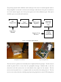
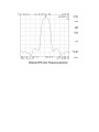
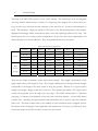
1
Stanford University Electrical Engineering
Space, Telecommunications, and
Radioscience (STAR) Laboratories
A tmospheric
W eather
E ducational
S ystem for
O bservation and
M odeling of
E lectromagnetic effects
Documentation
By Morris Cohen
Last modified August 30, 2005
Table of Contents
i.
Introduction to the Stanford University 2005 VLF receiver
ii.
Improvements in the Stanford University 2005 VLF receiver
iii.
Clock accuracy
iv.
Schematics
v.
Preamp DC biases
vi.
Parts list
vii.
Cabling pin connections
viii.
Calibration circuit
ix.
GPS Communication
x.
FPGA code
xi.
Antenna design
xii.
Dummy loop design
xiii.
Hum Sniffer Design
xiv.
Electric field reception
xv.
Testing and set-up
xvi.
Calibration and characterization instructions
xvii.
Using the software (written by Eddie Kim)
xviii.
Deployment checklist
xix.
Troubleshooting Guide
xx.
Additional comments/Undocumented changes
xxi.
Acknowledgements
xxii.
User Comments
i.
Introduction to the Stanford University 2005 VLF Receiver
The Stanford University Electrical Engineering Department’s Very Low Frequency (VLF) group is
engaged in studies of electromagnetic phenomenon in the ionosphere and magnetosphere. One of
the primary ways of studying these effects is through the use of ultra sensitive ground based VLF
receiver instruments, consisting of an antenna (or two) and electronics to process the antenna’s
signal. The electronics is designed to capture frequencies in the ELF/VLF range, which is roughly
30 Hz-50 kHz. By studying the data recorded from the antenna, a wide range of atmospheric effects
can be understood because they create disturbances in the typical magnetic field. A wide variety of
phenomenon can be studied with ELF/VLF receivers, including but not limited to: lightning
discharges (radio atmospherics), whistlers, lightning induced electron precipitation (LEP), cosmic
gamma-ray flares, terrestrial gamma-ray flashes (TGFs), sprites and other optical discharges, onehop and two-hop magnetospheric echo, ground-ionosphere coupling, solar flares, geomagnetic
storms, and more.
As such, the VLF group has been building and using VLF receivers for decades, refining the design
over the years. The receivers have reached the point of sensitivity where nearly any signal above the
ambient Earth noise floor can be detected. For example, it will pick up the miniscule signal from a
digital watch in the vicinity. This is important because some of the observed disturbances in the
electromagnetic field are very small.
In spring 2003, Justin Tan and Morris Cohen began building the newest incarnation, and it was
completed in fall 2004. A prototype line receiver, modeled almost exactly off of an older version,
was completed in June 2003. Full development began in autumn 2004, and was assembled in spring
2004. Initial field testing and final changes were made during summer 2004.
A number of
deployments occurred in fall 2004, during which time the support structures were finalized, and this
documentation packet was formed. At that point, the receiver was named the Atmospheric Weather
Educational System for Observation and Modeling of Effects, or, the AWESOME receiver. It was
named as such because it arose out of a partnership between the VLF group, headed by Umran
Inan, and the Solar Physics group, led by Phil and Deborah Scherrer. Its primary purpose originally
was to serve as a tool for educational outreach in schools across America, and eventually the world.
From this point on, the receiver will be referred to as the AWESOME monitor. Though based on
previous designs, the newest version adds a number of new improvements and modifications over
the old VLF receivers, to be highlighted later. The rest of this packet will discuss the design, use,
and performance of the 2005 VLF receiver.
Note that this documentation report will focus on specific working and use of this design and
implementation, including the receiver electronics, all the supporting hardware and software,
information needed to build and deploy, etc. For a more technical report on the design criteria for
VLF receivers, performance calculations, etc, refer to Evans Paschal’s report The Design of BroadBand VLF Receivers with Air-Core Loop Antennas. This report and its conclusions laid the
groundwork for some of the most important aspects of the AWESOME monitor.
The data from the 2005 VLF receiver is often used in one of two ways: Broadband analysis and
narrowband analysis. In broadband analysis, the entire frequency spectrum between the cutoffs is
retained, and often presented in the form of a spectrogram. Shown here is an example of a
spectrogram, created by MATLAB. It shows the frequency content over a 10 second snippet. The
red areas indicate strong signals at that frequency and that time, while the yellow and blue areas
indicate a weak and very weak presence at those frequencies.
In this example, there is a strong single frequency signal at 5 kHz (injected externally at the input)
for the first seven seconds (indicated by the horizontal red line), that then drifts around for the last
few seconds (turning the knob on the signal generator). There is also a broadband signal appearing
once per second (this was a test calibration signal to be discussed later). The noise floor is a bit
elevated around 10 kHz as can be seen by the yellowing there. The color scale is in decibels. This
spectrogram represents one channel of data.
Narrowband analysis is done a little differently. The data stream is filtered out except for one very
small frequency band (usually corresponding to a VLF transmitter frequency). Using fourier analysis
and demodulation, the amplitude and phase at that frequency can be determined and recorded (this
is done in software). Narrowband analysis is particularly valuable when VLF instruments are in
remote areas, with limited ability to transmit data back to Stanford. The narrowband data would
look something like this (amplitude shown only – data taken from http://wwwstar.stanford.edu/~hail/exdata.html,
Stanford
VLF
group)
Figure 1 illustrates the basic block diagram of the VLF receiver The 2005 VLF receiver consists of
three main components: First, an antenna to create electrical signals from electromagnetic field
disturbances. Second is a preamplifier to amplify the signal without introducing much noise, and
driving the signal over a long cable. The cable runs to a line receiver which filters and processes the
data so it can be recorded. In addition, the line receiver synchronizes the data with a GPS timing
signal, and passes those to a PC, with running software that records the signal and times.
1Ω 1mH
Antenna
Preamp
Line
Receiver
PC
GPS
Receiver
Figure 1: 2004 VLF Receiver Block Diagram
The antenna used is a magnetic loop, made by wrapping wire in a circle so that magnetic field
changes create small currents in the antenna. The antenna can be made arbitrarily large or small
(larger antennas will be more sensitive), the only restriction on the antenna is that the resistance of
the wire loop be 1 Ω, and the inductance be 1 mH, as the electronics are designed for these
characteristics. Further technical detail on different sizes and configurations to make a valid 1 Ω, 1
mH antenna can be found in the Paschal report. The antenna is best placed in a “quiet” area, as far
as possible from electromagnetic noise sources like power lines, generators, buildings. Since the
antenna is built from a planar loop of wire, it will only capture signals propagating with a magnetic
field component in the plane. Thus, in order to capture signals from all azimuths, it is necessary to
set up two antennas, orthogonal to each other. Generally, one antenna captures the North/South
component of incoming signals, and a second antenna captures the East/West component. It is
possible, however, to orient the two antennae in any desired configuration. All the signal electronics
in the preamp and line receiver are designed for two antenna channels, though one can be left out if
it is not needed for a particular application. So this receiver is not designed to capture signals with
three degrees of freedom (ie, like nearfield radiation).
E/W Antenna
N/S Antenna
Preamp
North
Figure 2: VLF Two Channel Orthogonal Magnetic Loop Antenna Configuration
Figure 3 illustrates the block diagram of the preamplifier. The preamp should be placed as close as
possible to the antenna, so that small signals aren’t attenuated over long cables. Since the antenna is
outdoors, the preamplifier must be housed in a weatherproof container.
The preamplifier’s
electronic operation is relatively simple compared to the line receiver’s. This is intentional, in order
to minimize interference into the antenna. The main amplification in the preamp comes from a
differential amplifier designed with discrete transistors. A very important component, though, is a
custom built transformer between the antenna and the transistors that closely matches the 1 Ω
resistance of the antenna to the small signal resistance of the transistor circuit. Following the
transistor amplifier, a number of op-amps buffer the signal, set the low frequency response cutoff,
and the gain. An RFI (radio frequency interference) suppression circuit is added to the front end.
Made from an LC low pass filter, this circuit ensures that high frequency signals like AM/FM radio
broadcast do not affect the electronics.
The preamp also includes a calibration circuit to determine the frequency response of the system.
The calibration circuit is described in detail in a later section, but it works by injecting a test signal at
the very front end of the preamplifier, and the output of the receiver could be read to determine the
system’s frequency response. The calibration circuit is activated by the line receiver, which provides
power to run it.
The preamp is placed inside a NIMA-4 rated weather proof box since it is normally placed outdoors.
The preamplifier is connected to the line receiver through a cable that has four pairs of conductors:
two for the antenna signals, one for the power signals, one for the calibration signal. Each pair is
shielded to prevent crosstalk and interference.
RFI
Suppression
Signal
Transformer
Input from
Antenna
Differential
Amplifier
Adjustable
Filter and
Gain
Output to Line
Receiver
Output
Coupling
Transformer
Figure 3: Preamplifier Block Diagram
Preamplifier From Outside
Open Preamplifier Box
The line receiver’s operations are noticeably more complicated than the preamp’s. The line receiver
should be placed 100 ft or more from the preamplifier through a shielded cable, so that the
electronics in the line receiver does not emit radiation that couples into the antenna. The line
receiver must be placed close to a computer which can record the data coming from it. The line
receiver serves many functions, including signal processing, digitization control, GPS management,
power management, and system calibration. The line receiver is placed in a custom built box though
it is not designed for outdoor use.
In processing the signal, the line receiver includes a clip protection circuit, which clips the top of
signals when they get too strong (and sets of an indicator light). If calibrated correctly, though, this
should only be triggered in the event of exceptionally strong signals or an electrical failure. The
most important part, though, is an anti-aliasing filter. For most VLF group applications, the data is
sampled at 100 kHz, thus the anti-aliasing filter should be fixed between 40 and 50 kHz. A pair of
identical filter chips 12 poles total takes care of that filtering.
Line Receiver Front
Line Receiver Back
Line Receiver Inside
One of the key requirements for the 2005 VLF receiver is very high accuracy sampling, in order to
synchronize the sampling in different systems and provide precise phase information in narrowband
analysis. This requirement is met by providing the ADC card with a low-skew, low-draft clock. The
line receiver does this by using a GPS locked signal, and a trim-adjustable 10 MHz oscillator. Using
the GPS timing signal (1 Hz), and a feedback circuit, the 10 MHz clock is adjusted so that it is as
accurate as possible. The 100 kHz sampling signal is generated from this accurate clock. The details
and performance characteristics of this are included later.
The GPS signal needed for this circuit comes in from an antenna and is attached to an on-board
card made by Motorola. The GPS antenna does not need to be in a quiet location, but it should
have a clear view of much of the sky in order to communicate with GPS satellites. An FPGA in the
line receiver communicates with the Motorola board and uses it to synchronize the sampling clock,
and to provide a time stamp for all the data through a serial port.
The line receiver is also responsible for providing power to the preamplifier.
The power is
generated from 60 Hz, 110V AC power by an external power supply inside the line receiver box. If
using in an area that does not provide 60 Hz 110 V power, you will need to find a way to convert
your power, or to drive the line receiver’s DC input voltages directly from an external source. The
voltages +/- 15 V are delivered along the same cable that brings the signals from the preamp (the
shielding of the cable pairs enables this to be possible without degradation of the data).
Finally, the line receiver controls and activates the calibration circuit in the preamp, by sending a 15
V power signal over the cabling. The FPGA on board also controls this, activating the calibration
circuit at predetermined internals by turning on a transistor driver circuit.
Input from
Preamp
Clip Light
Indicator
Input
Coupling
Transformer
Clipper and
Comparator
AntiAliasing
Filter
Output to
ADC Card
Output to
Preamp
Calibration
Circuit
Driver
FPGA
Output to
Serial port
+/- 15V
10 MHz
Oscillator
GPS
Antenna
Figure 4: Line Receiver Block Diagram
The data is usually digitized with a card installed in the PC. The card used is made by National
Instruments, and goes into a PCI slot in the computer. Alternatively, a PCMCIA version is available
for a laptop computer. The PC has installed software, created by the VLF group, that is capable of
producing raw MATLAB data files, demodulating and breaking down the data for selected
frequencies (narrowband studies), and sending the information over the internet (ftp).
ii.
Improvements to the Stanford University 2005 VLF Receiver
The AWESOME monitor includes a number of modifications in electrical performance, mechanical
layout, cost, and ease of use. Since some users of the AWESOME receiver may already be familiar
with older design iterations, it is helpful to highlight these changes and additions specifically.
Elimination of line driver circuit: The previous VLF receivers contained an elaborate line driver
card in the preamplifier, in order to drive the signal over as much as 2000 ft of cabling to the line
receiver. In AWESOME, this whole card was eliminated, and the output op-amp in the preamp
card was swapped with one that has more output drive ability. This greatly simplifies the design of
the preamplifier.
Elimination of 35 V preamp supply: In previous designs, the preamp was powered from a 35 V
signal coming from the line receiver. The 35 V was generated in the line receiver directly from 110V
AC power. Once in the preamp, this 35 V single ended voltage would then be regulated into a +/15 V bipolar supply. The chief disadvantage was that the preamp and line receiver had different
grounds (ground for the preamp was at +17.5 V for the line receiver), which made it impossible to
probe signals in the preamplifier without shorting out the DC signals.. Instead, the AWESOME
receiver sends a direct +/- 15 V signal from the line receiver to the preamplifier. This removes the
AC-DC regulation circuit in the line receiver and the DC-DC regulation in the preamp.
Single cable connection between line receiver and preamp: The former VLF receivers had two
coaxial BNC cables, one for each channel, connecting the preamplifier to the line receiver. The N/S
channel also transmitted the 35 V power signal. This has been replaced with a new four-pair
shielded cable made by Belden, the 1217B. Not only has the power signal been decoupled from the
transmission line for the signals, but there is now only one cable instead of two, and the 75 Ω
impedance of the cable used reduces the signal attenuation for the long cable lengths.
Improvements in low frequency response: Though previous VLF receivers were deployed in places
that required measurements of frequencies as small as 30 Hz, a number of undocumented hardware
changes were required in order to achieve this response. This is mostly because the older version
was designed primarily to be a narrowband system, optimized for the frequency range of 10-40 kHz.
In addition, the line transformers, on either side of the transmission lines, had some peaking at in
the frequency response at about 1 kHz and began to rolloff a little below that. AWESOME is
designed by default to work at frequencies as low as 30 Hz. The newer version replaces the line
transformer with a better one, which has a lower cutoff.
Improvements in high frequency response: Our VLF receiver systems are sampled at 100 kHz,
which is why the anti-aliasing filter is set at 40 kHz or so. The new receivers implement this filter
with a sharper circuit (LTC1562), which has both a flatter response in the passband, and a sharper
brick wall response. As a result, the new anti-aliasing filter raises the bandwidth of useful data to 4547 kHz. The filter cuts off at 47 kHz, and reaches 100 dB of attenuation by 55 kHz, ensuring that
data up to 45 kHz is free of aliasing. These `two pictures show the improved anti-aliasing filtering
of the AWESOME monitor. The red line indicates the amplitude, and the blue line indicates the
phase.
Old VLF Receiver Frequency Response
Elimination of external GPS clock:
New VLF Receiver Frequency Response
The older VLF systems used a GPS receiver made by
TrueTime. The key advantage to it was that it provided not only the 1 Hz GPS signal but also a 100
kHz signal (used for sampling) that is synchronized with the GPS signal and thus very exact (as
described earlier, this is important in order to get accurate phase information and to compare data
from site to site). In the 2005 VLF receiver, this has been eliminated and replaced with a Motorola
GPS receiver contained within the line receiver. Though the Motorola GPS receiver does not
generate the 100 kHz GPS-synchronized clock, a frequency-locked loop consisting of a 10 MHz
oscillator, an FPGA and a D/A converter (all this is detailed later) generates the 100 kHz sampling
signal within the line receiver. The elimination of the external GPS clock saves substantial cost and
means one less component to bring and set up at a VLF reception site. Removing the external GPS
receiver reduces the physical size of all the equipment, and eliminates a major cost.
Smaller and lighter preamp box: The physical size of the preamp has been shrunk considerably.
Formerly placed in a box with 14” x 16” base, and 7” height, the preamp now measures 8” x 10”
base and 5” height (about four times less volume).
Smaller, lighter, more stable line receiver box: The line receiver as well was placed in a better box.
The old boxes had a 10” x 12” base and 6” height, whereas the new boxes are 7” x 10” with a 5”
height (about half the volume). The new boxes are also more stable, with a two piece design rather
than the older completely disassembled frame boxes.
Modular card design and solder-less layout: The AWESOME receiver was designed with ease of
testing and debugging in mind. The older version had modular cards in the preamplifier, but the
cards were connected to a backplane that required hours to wire up manually to the inputs and to a
monitor and control board. The older line receiver placed everything on one large circuit board,
with a lot of soldered connections to the box, so that removal of the card for testing or debugging
required cutting a dozen or so wires that had to be re-soldered into place later. The new receiver has
modular cards for the filter/clip chips in the line receiver (on each channel), and the amplifier cards
in the preamp. The modular design also enables a one channel system to be converted to twochannel with much more ease. The input and connections to the box were all made with Molex
power plugs rather than permanent soldering. Though a slight contact resistance is introduced
(replacing a solder joint resistance), the main boards in each box can be detached from its
surroundings and removed in a matter of seconds for easy replacement, testing, or debugging.
New repeatable dummy loop design: A device called a dummy loop emulates the impedance of the
antenna and allows test signals to be injected into the VLF system. The previous VLF receiver did
not include an accompanying dummy loop design, so dummy loops were often built by hand,
individually.
As part of the AWESOME package, a new repeatable dummy loop has been
completely designed and specified, and a sufficient number will be made so that VLF systems can be
readily tested when needed.
New repeatable antenna design: The support structure for the wire loop antennas was previously
not documented and often built ad hoc. Accompanying the 2005 VLF receiver is a repeatable,
clearly specified method for building two orthogonal antennas and a support structure.
New repeatable hum sniffer design: Site selection is facilitated by the use of a hum sniffer, a
miniaturized, portable version of the VLF system. The hum sniffer uses a small antenna, and
outputs its signal to a laptop, for quick characterization of electromagnetic environment. The 2005
VLF receiver includes a fully specified and repeatable design for a hum sniffer.
Ease of duplication and change: The AWESOME monitor includes a complete parts list, including
price, part number, and manufacturers. Also included is software to reproduce the circuit boards,
box, and every other parts. For future VLF receiver needs, as well as for future design changes,
individual portions can be modified and change, without redoing the entire system from scratch as
was done for this iteration.
E-field preamp; The AWESOME monitor can be adapted for picking up electric field signals
instead of or along with magnetic field signals, through the use of a dipole whip antenna, and a
different preamp card. This is detailed in the later sections.
iii.
Sampling Clock Feedback for Accurate Phase Information
One of the most important features of the 2005 VLF receiver is the ability to produce a very exact
100 kHz signal for sampling. This signal is synchronized with a GPS signal and has very small error.
When the error is small enough, the data retrieved can be compared from site to site, and in
addition, the phase information gathered in the narrowband analysis becomes much more exact.
Older versions used an external GPS clock made by TrueTime to provide the 100 kHz signal, but
the 2005 model introduces a frequency locked loop to achieve the same result. Figure 5 shows the
hardware block diagram
10-Bit D/A
Converter
1 Hz GPS
Signal
10 MHz
Adjustable
Oscillator
FPGA
Divider
100 kHz
Sampling
Clock
FPGA
Counter
Figure 5: Clock Maintenance Circuit
The FPGA is the main component here. It counts cycles from the 10 MHz oscillator between every
1 Hz GPS pulse, and if the number is greater or less than 10,000,000, the FPGA will change the
value of the D/A converter’s inputs, which thereby adjust the oscillator accordingly. The accurate
10 MHz clock is divided down to 100 kHz. Since the 10 MHz signal is synchronized every second,
as long as the count rate of the oscillator remains at 10,000,000, the frequency remains accurate
within 1 Hz, this the error of the sampling clock will be better than 0.1 parts per million (ppm)1.
Since the error stretches over 1 s (between GPS synchronizations), that corresponds to 100 ns of
1
The feedback should be able to improve further on 0.1 ppm since even fractions of a count per second error will eventually lead to
clock adjustment. But since 0.1ppm is already below the GPS error we will stay conservative.
maximum skew at any time. Since the GPS signal itself has a built-in skew of 200 ns, the total error
in the sampling clock is 300 ns, or 0.3 ppm.
Since a 20 kHz signal propagates one degree of phase in 111 ns, and the sampling clock’s error is 0.3
ppm, or 300 ns, the phase error at 25 kHz will be 300/139 = 2.16º. Two thirds of this error
originates from jitter in the GPS signal, which is the limiting error in this scheme. The phase error
at higher and lower frequencies will be scaled proportionately to 20 kHz and 2.16º (i.e. a 10 kHz
signal has a phase error of 2.16º/2 = 1.08º).
The circuit was tested in two ways: First, the oscillator output was connected to a network analyzer
which plotted the frequency content of the 10 MHz signal. When the power was turned on, you
could visibly see the frequency start at some amount above or below 10 MHz and then slowly (over
a few minutes time) zoom in toward 10 MHz exactly. The plots of the steady states taken from the
Network Analyzer are shown below. In a second test, the FPGA was programmed to output a
digital signal whenever the 10 MHz clock deviated enough to warrant adjusting the DAC.
Additionally, the drift between the two signals could be observed on a fast oscilloscope, and it was
observed that the new 100 kpps signal drifted by less than 300 ns at any time.
iv.
Hardware Schematics
The following hardware schematics and layout drawings are included:
1. Preamplifier Backplane
2. Preamplifier Gain Card
3. Preamplifier Gain Card Layout
4. Line Receiver Motherboard
5. Line Receiver Motherboard Layout
6. Line Receiver Filter Card
7. Line Receiver Sideboard
8. Electric field preamplifier card
v.
Preamp DC Biases
The following diagram shows the DC biases for the preamp transistor circuit. This may be useful
for troubleshooting or for future design changes.
vi.
Parts List
Here is a parts list for the 2005 Stanford VLF receiver
VLF System
Line Receiver
Qty
1
2
1
1
1
Description
Motherboard
Filter Cards
Sideboard
External Power Supply
Box
Supplier
Advanced Circuits
Advanced Circuits
Advanced Circuits
PowerOne
ProtoCase
Part #
Custom Made
Custom Made
Custom Made
HAD15-0.4-A
Custom Made
Supplier
Advanced Circuits
Advanced Circuits
Adalet
Part #
Custom Made
Custom Made
JN4XHA-100804
Supplier
Synergy Systems
Synergy Systems
Home Depot
Part #
10001339
Preamp
Qty
1
2
1
Description
Backplane
Preamp Cards
Box
GPS
Qty
1
1
1
Description
Vic100 GPS Timing Antenna w/ Pipe Clamp
GPS N-connector Cable (50m)
10ft 1.5 in PVC piping with connector parts
Cable Assembly
Qty
1
2
Description
Four Twisted Pair Shielded Cable (250 ft)
Amphenol 12 Pin Cable Connector with Sockets
Supplier
Belden
Digikey
Part #
1217B
97-3106A-20-27S
Supplier
Part #
Digikey
MS3106R-10SL-3S
Antenna
Qty
123
ft
2
Description
Wire 14 AWG
Amphenol 3 Pin Cable Connector with Rocker
A/D System
Qty
Description
1
NIDAQ Card 6034E
1
50 Pin Cable SH6850
Supplier
National
Instruments
National
Instruments
Part #
187576C-01
776784-01
Line Receiver
Motherboard
Ref
C1
C2
C3
C4
C5
C6
C7
C8
C9
C10
C11
C12
C13
C14
C15
C16
C17
C18
C19
C20
C21
C22
C23
C24
C25
C26
C27
C28
C29
C30
C31
C32
Value
4.7 nF
4.7 nF
10 uF
4.7 nF
4.7 nF
0.1 uF
0.1 uF
0.1 uF
0.1 uF
47 nF
0.1 uF
0.33 uF
1.0 uF
0.1 uF
0.1 uF
1.0 uF
0.1 uF
0.1 uF
1.0 uF
0.1 uF
0.1 uF
0.1 uF
0.1 uF
1.0 uF
1.0 uF
0.1 uF
0.1 uF
1.0 uF
0.1 uF
1.0 uF
1.0 uF
Small
Description
Ceramic Capacitor
Ceramic Capacitor
Tantalum Capacitor
Ceramic Capacitor
Ceramic Capacitor
Ceramic Capacitor
Ceramic Capacitor
Ceramic Capacitor
Ceramic Capacitor
Ceramic Capacitor
Ceramic Capacitor
Ceramic Capacitor
Tantalum Capacitor
Ceramic Capacitor
Ceramic Capacitor
Tantalum Capacitor
Ceramic Capacitor
Ceramic Capacitor
Tantalum Capacitor
Ceramic Capacitor
Ceramic Capacitor
Ceramic Capacitor
Ceramic Capacitor
Tantalum Capacitor
Tantalum Capacitor
Ceramic Capacitor
Ceramic Capacitor
Tantalum Capacitor
Ceramic Capacitor
Tantalum Capacitor
Tantalum Capacitor
Optional - Typically left out
Supplier
Digikey
Digikey
Digikey
Digikey
Digikey
Digikey
Digikey
Digikey
Digikey
Digikey
Digikey
Digikey
Digikey
Digikey
Digikey
Digikey
Digikey
Digikey
Digikey
Digikey
Digikey
Digikey
Digikey
Digikey
Digikey
Digikey
Digikey
Digikey
Digikey
Digikey
Digikey
Part #
399-1335-ND
399-2155-ND
399-2155-ND
399-2155-ND
399-2155-ND
495-1069-1-ND
399-2155-ND
399-2174-ND
399-1337-ND
399-2155-ND
399-2155-ND
399-1337-ND
399-2155-ND
399-2155-ND
399-1337-ND
399-2155-ND
399-2155-ND
399-2155-ND
399-2155-ND
399-1337-ND
399-1337-ND
399-2155-ND
399-2155-ND
399-1337-ND
399-2155-ND
399-1337-ND
399-1337-ND
C33
C34
C35
C36
C37
C38
C39
0.1 uF
1.0 uF
1.0 uF
0.1 uF
1.0 uF
0.1 uF
0.1 uF
Ceramic Capacitor
Tantalum Capacitor
Tantalum Capacitor
Ceramic Capacitor
Tantalum Capacitor
Ceramic Capacitor
Ceramic Capacitor
Digikey
Digikey
Digikey
Digikey
Digikey
Digikey
Digikey
D1
1N4005
Diode
Digikey
D2
1N4005
Diode
Digikey
D3
J1
J2
J3
J4
J5
J6
J7
J8
J9
J10
L1
L2
L3
L4
Q1
Q2
R1
1N4148
Diode
12-Pin Power Header
50-Pin Right Angle Header
0.1" Jumper Header
44-Pin 0.1" Card Edge Connector
10-Pin 0.1" Protected Header
44-Pin 0.1" Card Edge Connector
0.1" Jumper Header
0.1" Jumper Header
0.1" Jumper Header
0.1" Jumper Header
Inductor
Inductor
Inductor
Inductor
PNP Transistor TO-92
NPN Transistor TO-92
1% Metal Film Resistor
Digikey
Digikey
Digikey
Digikey
Digikey
Digikey
Digikey
Digikey
Digikey
Digikey
Digikey
Digikey
Digikey
Digikey
Digikey
Digikey
Digikey
Digikey
1% Metal Film Resistor
Digikey
R2
R3
R4
R5
R6
R7
R8
R9
R10
R11
R12
R13
R14
R15
R16
R17
R18
R19
R20
22 uH
22 uH
22 uH
22 uH
2N3906
2N3904
4.7 kOhm
12.1
kOhm
N/A
47 Ohm
N/A
N/A
10 kOhm
N/A
75 Ohm
75 Ohm
953 Ohm
1 kOhm
250 Ohm
250 Ohm
1 kOhm
1 kOhm
1 kOhm
1 kOhm
1 kOhm
410 Ohm
Does not exist
1% Metal Film Resistor
Does not exist
Does not exist
1% Metal Film Resistor
Does not exist
1% Metal Film Resistor
1% Metal Film Resistor
1% Metal Film Resistor
1% Metal Film Resistor
1% Metal Film Resistor
1% Metal Film Resistor
1% Metal Film Resistor
1% Metal Film Resistor
1% Metal Film Resistor
1% Metal Film Resistor
1% Metal Film Resistor
1% Metal Film Resistor
Digikey
Digikey
Digikey
Digikey
Digikey
Digikey
Digikey
Digikey
Digikey
Digikey
Digikey
Digikey
Digikey
Digikey
399-2155-ND
399-1337-ND
399-1337-ND
399-2155-ND
399-1337-ND
399-2155-ND
399-2155-ND
1N4005RLOSCTND
1N4005RLOSCTND
WM1629
AHZ50K
4-103240-0
S1223
A26268
S1223
4-103240-0
4-103240-0
4-103240-0
4-103240-0
1530B225
1530B225
1530B225
1530B225
R21
T1
T2
TP1
U1
U2
U3
U4
U5
U6
U7
U8
U9
U10
U11
U12
U13
U14
U9*
U12*
350 Ohm
1% Metal Film Resistor
70.7 Line Audio Transformer
70.7 Line Audio Transformer
Test Point
Voltage Regulator uA7805 TO-220
Voltage Regulator uA7905 TO-220
4 Pin Power Header
Inverters 74ACT04
RS232 Chip Max3323 DIP
10-Bit D/A Converter THS5651 SOIC
10-Pin 0.1" Protected Header
9 Pin Serial Connector
44-Pin PLCC Socket
10 MHz Oscillator DIP
Inverters 74HC04
10-Pin 0.05" Header
Voltage Regulator LM317 TO-220
Voltage Regulator LM317 TO-220
Altera Max 7000AE EPM7064AE
Motorola GPS M12+ Timer Card
Digikey
Stancor
Stancor
Digikey
Digikey
Digikey
Digikey
Digikey
Maxim
Digikey
Digikey
Digikey
Digikey
Vectron
Digikey
Samtec
Digikey
Digikey
Arrow
Synergy Systems
A-8096
A-8096
296-13996-5-ND
LM7905CTNS-ND
WM1626
MAX2232
296-2992-5-ND
A26268
309M
AE7328
VTA1-1B1-10M000
296-12772-5-ND
SFMC-105-01-S-D
LM317HVT-ND
EPM7064AELC44-7
LTC1562 Filter Card
Ref
C1
C2
C3
C4
C5
C6
C7
C8
C9
C10
C11
C12
C13
C14
C15
C16
C17
C18
C19
C20
C21
C22
C23
Value
10 pF
0.1 uF
1.0 uF
0.1 uF
1.0 uF
4.7 uF
47 pF
0.1 uF
1.0 uF
0.1 uF
1.0 uF
39 pF
27 pF
390 pF
0.1 uF
1.0 uF
0.1 uF
1.0 uF
33 pF
0.1 uF
1.0 uF
0.1 uF
1.0 uF
Description
Ceramic Capacitor
Ceramic Capacitor
Tantalum Capacitor
Ceramic Capacitor
Tantalum Capacitor
Ceramic Capacitor
Ceramic Capacitor
Ceramic Capacitor
Tantalum Capacitor
Ceramic Capacitor
Tantalum Capacitor
Ceramic Capacitor
Ceramic Capacitor
Ceramic Capacitor
Ceramic Capacitor
Tantalum Capacitor
Ceramic Capacitor
Tantalum Capacitor
Ceramic Capacitor
Ceramic Capacitor
Tantalum Capacitor
Ceramic Capacitor
Tantalum Capacitor
Supplier
Digikey
Digikey
Digikey
Digikey
Digikey
Digikey
Digikey
Digikey
Digikey
Digikey
Digikey
Digikey
Digikey
Digikey
Digikey
Digikey
Digikey
Digikey
Digikey
Digikey
Digikey
Digikey
Digikey
Part #
C24
C25
C26
C27
C28
C29
C30
C31
C32
C33
D1
D2
D3
D4
R1
R2
R3
R4
R5
R6
R7
R8
R9
R10
R11
R12
R13
R14
R15
R16
R17
R18
R19
R20
R21
R22
R23
R24
R25
8.2 pF
15 pF
0.1 uF
1.0 uF
0.1 uF
1.0 uF
0.1 uF
1.0 uF
0.1 uF
1.0 uF
1N4005
1N4005
1N4005
1N4005
20 kOhm
130
kOhm
10 kOhm
150
kOhm
75 kOhm
133
kOhm
40.2
kOhm
60.4
kOhm
5 kOhm
47 Ohm
1.75
kOhm
56.2
kOhm
105
kOhm
5 kOhm
210
kOhm
48.7
kOhm
20 kOhm
107
kOhm
105
kOhm
3 kOhm
3.9 kOhm
4 kOhm
3 kOhm
3.9 kOhm
13.7
Ceramic Capacitor
Ceramic Capacitor
Ceramic Capacitor
Tantalum Capacitor
Ceramic Capacitor
Tantalum Capacitor
Ceramic Capacitor
Tantalum Capacitor
Ceramic Capacitor
Tantalum Capacitor
Multiplexer SOIC-20
Multiplexer SOIC-20
4082
Multiplexer SOIC-20
1% Metal Film Resistor
Digikey
Digikey
Digikey
Digikey
Digikey
Digikey
Digikey
Digikey
Digikey
Digikey
Digikey
Digikey
Digikey
Digikey
Digikey
1% Metal Film Resistor
Digikey
1% Metal Film Resistor
Digikey
1% Metal Film Resistor
Digikey
1% Metal Film Resistor
Digikey
1% Metal Film Resistor
Digikey
1% Metal Film Resistor
Digikey
1% Metal Film Resistor
Digikey
1% Metal Film Resistor
1% Metal Film Resistor
Digikey
Digikey
1% Metal Film Resistor
Digikey
1% Metal Film Resistor
Digikey
1% Metal Film Resistor
Digikey
1% Metal Film Resistor
Digikey
1% Metal Film Resistor
Digikey
1% Metal Film Resistor
Digikey
1% Metal Film Resistor
Digikey
1% Metal Film Resistor
Digikey
1% Metal Film Resistor
Digikey
1% Metal Film Resistor
1% Metal Film Resistor
1% Metal Film Resistor
1% Metal Film Resistor
1% Metal Film Resistor
1% Metal Film Resistor
Digikey
Digikey
Digikey
Digikey
Digikey
Digikey
R26
R27
R28
R29
R30
R31
R32
R33
R34
R35
R36
R37
R38
R39
kOhm
150
kOhm
316
kOhm
45.3
kOhm
698
kOhm
32.4
kOhm
10 kOhm
10 kOhm
10 kOhm
10 kOhm
20 kOHm
22.6
kOhm
47 Ohm
2.2 kOhm
22.6
kOhm
U1
U2
U3
U4
U7
U8
1% Metal Film Resistor
Digikey
1% Metal Film Resistor
Digikey
1% Metal Film Resistor
Digikey
1% Metal Film Resistor
Digikey
1% Metal Film Resistor
Digikey
1% Metal Film Resistor
1% Metal Film Resistor
1% Metal Film Resistor
1% Metal Film Resistor
1% Metal Film Resistor
Digikey
Digikey
Digikey
Digikey
Digikey
1% Metal Film Resistor
Digikey
1% Metal Film Resistor
1% Metal Film Resistor
Digikey
Digikey
1% Metal Film Resistor
Digikey
LTC1562 Filter Chip
LM318 Op-Amp
LM339 Comparator Quad
LTC1562 Filter Chip
BUF634 Buffer Chip
LM318 Op-Amp
Digikey
Digikey
Digikey
Digikey
Digikey
Digikey
Sideboard
Ref
D1
D2
D3
J1
J2
R1
R2
R3
U2
Value
LED
LED
LED
60 Ohm
270 Ohm
600 Ohm
Description
Red LED
Red LED
Blue LED
Vertical BNC Connector
Vertical BNC Connector
1% Metal Film Resistor
1% Metal Film Resistor
1% Metal Film Resistor
10-Pin 0.1" Protected Header
Supplier
Digikey
Digikey
Digikey
Digikey
Digikey
Digikey
Digikey
Digikey
Digikey
Part #
MV3750
MV3750
67-1750
A24513
A24513
A26268
Box Assembly Parts
Qty
16
1
1
Description
Female Crimp Terminals
12 Pin Receptacle
12-Pin Box Mount Connector
Supplier
Digikey
Digikey
Digikey
Part #
WM1101
WM1337
97-3102A-20-27P
1
4
1
1
1
1
1
8
1
1
4-Pin Receptacle
Screws 6-32 0.25"
Fuseholder
Fuse, Slow Blow 1/8W
60 Hz 110V EMI Filter
10 Pin Ribbon Cable 6"
Power Switch
Box Screws
Metal Enclosure for AC Power Input
MMCX to N-Type Connector
Digikey
WM1333
Digikey
F1488
Digikey
Digikey
Digikey
CCM1101-ND
C3AAT-1006G
CH755-ND
Home Depot
Synergy Systems
50169 00500
Preamplifier
Backplane
Ref
C25
C26
D1
D2
D3
D4
D5
J1
J2
J3
J8
J9
R1
R2
R3
R4
R5
R6
T1
T2
U1
U2
Value
10 uF
0.1 uF
1N4005
LED
LED
LED
LED
1.75
kOhm
1.75
kOHm
200 Ohm
200 Ohm
200 Ohm
200 Ohm
Description
Tantalum Capacitor
Ceramic Capacitor
Diode
Red LED
Red LED
Red LED
Red LED
12-Pin Power Header
44 Pin 0.156" Card Edge Connector
44 Pin 0.156" Card Edge Connector
4-Pin Power Header
4-Pin Power Header
Supplier
Digikey
Digikey
Digikey
Digikey
Digikey
Digikey
Digikey
Digikey
Digikey
Digikey
Digikey
Digikey
1% Metal Film Resistor
Digikey
1% Metal Film Resistor
Digikey
1% Metal Film Resistor
1% Metal Film Resistor
1% Metal Film Resistor
1% Metal Film Resistor
25 Volt Audio Line Transformer
25 Volt Audio Line Transformer
Monitor Switch
Voltage Regulator uA7805 TO-220
Digikey
Digikey
Digikey
Digikey
Stancor
Stancor
Digikey
Digikey
Preamp Card
Part #
MV3750
MV3750
MV3750
MV3750
WM1629
S5223
S5223
WM1626
WM1626
A8096
A8096
EG1951
296-13996-5-ND
Ref
C1
C2
C3
C4
C5
C6
C7
C8
C9
C10
C11
C12
C13
C14
C15
C16
C17
C18
C19
C20
C21
C22
C23
C24
C25
C26
C27
C28
C29
C30
C31
C32
C33
C34
C35
C36
C37
D1
D2
D3
J1
J4
JP2
L1
L2
Q1
Q2
Value
22 nF
22 nF
22 nF
22 nF
22 uF
22 uF
0.1 uF
10 pF
10 pF
22 uF
0.47 uF
10 nF
3.3 nF
3.3 nF
0.1 uF
0.1 uF
3.3 nF
3.3 nF
4.7 uF
27 pF
0.1 uF
0.1 uF
4.7 uF
1.0 uF
0.1 uF
1.0 uF
0.1 uF
22 uF
22 uF
0.1 uF
0.1 uF
0.1 uF
10 uF
0.1 uF
0.1 uF
0.1 uF
0.1 uF
1N4148
1N4148
1N4148
10 uH
10 uH
2N4250
2N4250
Description
Ceramic Capacitor
Ceramic Capacitor
Ceramic Capacitor
Ceramic Capacitor
Tantalum Capacitor
Tantalum Capacitor
Ceramic Capacitor
Ceramic Capacitor
Ceramic Capacitor
Tantalum Capacitor
Tantalum Capacitor
Polyprolylene Capacitor
Ceramic Capacitor
Ceramic Capacitor
Ceramic Capacitor
Ceramic Capacitor
Ceramic Capacitor
Ceramic Capacitor
Ceramic Capacitor
Ceramic Capacitor
Ceramic Capacitor
Ceramic Capacitor
Ceramic Capacitor
Tantalum Capacitor
Ceramic Capacitor
Tantalum Capacitor
Ceramic Capacitor
Tantalum Capacitor
Tantalum Capacitor
Ceramic Capacitor
Ceramic Capacitor
Ceramic Capacitor
Tantalum Capacitor
Ceramic Capacitor
Ceramic Capacitor
Ceramic Capacitor
Ceramic Capacitor
Diode
Diode
Diode
0.1" Jumper Header
0.1" Jumper Header
0.1" Double Jumper Header
Inductor
Inductor
PNP Bipolar Transistor
PNP Bipolar Transistor
Supplier
Digikey
Digikey
Digikey
Digikey
Digikey
Digikey
Digikey
Digikey
Digikey
Digikey
Digikey
Digikey
Digikey
Digikey
Digikey
Digikey
Digikey
Digikey
Digikey
Digikey
Digikey
Digikey
Digikey
Digikey
Digikey
Digikey
Digikey
Digikey
Digikey
Digikey
Digikey
Digikey
Digikey
Digikey
Digikey
Digikey
Digikey
Digikey
Digikey
Digikey
Digikey
Digikey
Digikey
Digikey
Digikey
Digikey
Digikey
Part #
399-2006-ND
399-2006-ND
399-2006-ND
399-2006-ND
399-1531-ND
399-1531-ND
399-2054-ND
399-1888-ND
399-1888-ND
399-1531-ND
399-1443-ND
399-2001-ND
399-2001-ND
399-2054-ND
399-2054-ND
399-2001-ND
399-2001-ND
399-1302-ND
399-1891-ND
399-2054-ND
399-2054-ND
399-1302-ND
399-2054-ND
399-2054-ND
399-1531-ND
399-1531-ND
399-2054-ND
399-2054-ND
399-2054-ND
399-2054-ND
399-2054-ND
399-2054-ND
399-2054-ND
4-103240-0
4-103240-0
4-103240-0
PN4250-ND
PN4250-ND
Q3
Q4
Q5
Q6
Q7
R1
R2
R3
R4
R5
R6
R7
R8
R9
R10
R11
R12
R13
R14
R15
R16
R17
R18
R19
R20
R21
R22
R23
R24
R25
R26
R27
2N4250
2N4250
2N4250
2N4250
2N4250
267
kOhm
267
kOhm
200
kOhm
200
kOhm
1.75
kOhm
500 Ohm
22.6
kOhm
22.6
kOhm
9.09
kOhm
48.7
kOhm
1 MOhm
48.7
kOhm
48.7
kOhm
1 MOhm
267
kOhm
267
kOhm
232
kOhm
232
kOhm
21.5
kOhm
27.4
kOhm
27.4
kOhm
267
kOhm
10 kOHm
11.5
kOHm
4.12
kOhm
26.7
kOhm
Open
PNP Bipolar Transistor
PNP Bipolar Transistor
PNP Bipolar Transistor
PNP Bipolar Transistor
PNP Bipolar Transistor
Digikey
Digikey
Digikey
Digikey
Digikey
1% Metal Film Resistor
Digikey
1% Metal Film Resistor
Digikey
1% Metal Film Resistor
Digikey
1% Metal Film Resistor
Digikey
1% Metal Film Resistor
Digikey
Potentiometer
Digikey
1% Metal Film Resistor
Digikey
1% Metal Film Resistor
Digikey
1% Metal Film Resistor
Digikey
1% Metal Film Resistor
Digikey
1% Metal Film Resistor
Digikey
1% Metal Film Resistor
Digikey
1% Metal Film Resistor
Digikey
1% Metal Film Resistor
Digikey
1% Metal Film Resistor
Digikey
1% Metal Film Resistor
Digikey
1% Metal Film Resistor
Digikey
1% Metal Film Resistor
Digikey
1% Metal Film Resistor
Digikey
1% Metal Film Resistor
Digikey
1% Metal Film Resistor
Digikey
1% Metal Film Resistor
Digikey
1% Metal Film Resistor
Digikey
1% Metal Film Resistor
Digikey
1% Metal Film Resistor
Digikey
1% Metal Film Resistor
Digikey
Open Circuit - Do Not Populate
Digikey
PN4250-ND
PN4250-ND
PN4250-ND
PN4250-ND
PN4250-ND
R28
R29
R30
R31
R32
R33
R34
R35
R36
R37
R38
R39
R40
R41
R42
R43
R44
R45
R46
R47
R48
R49
R50
R51
T1
TP1
TP2
TP3
TP4
U1
U2
U3
U4
U6
U7
U8
U11
U12
U13
28.7
kOhm
6.81
kOhm
2 kOhm
10 kOhm
61.9
kOhm
100 Ohm
100
kOhm
100
kOhm
100
kOhm
100
kOhm
243 Ohm
1.75
kOhm
243 Ohm
1.75
kOhm
10 kOhm
10 kOhm
100 Ohm
100 Ohm
2.21
kOhm
2.21
kOhm
6.34
kOhm
6.34
kOhm
10 kOhm
5 kOhm
1% Metal Film Resistor
Digikey
1% Metal Film Resistor
Digikey
1% Metal Film Resistor
1% Metal Film Resistor
Digikey
Digikey
1% Metal Film Resistor
Digikey
1% Metal Film Resistor
Digikey
1% Metal Film Resistor
Digikey
1% Metal Film Resistor
Digikey
1% Metal Film Resistor
Digikey
1% Metal Film Resistor
Digikey
1% Metal Film Resistor
Digikey
1% Metal Film Resistor
Digikey
1% Metal Film Resistor
Digikey
1% Metal Film Resistor
Digikey
1% Metal Film Resistor
1% Metal Film Resistor
1% Metal Film Resistor
1% Metal Film Resistor
Digikey
Digikey
Digikey
Digikey
1% Metal Film Resistor
Digikey
1% Metal Film Resistor
Digikey
1% Metal Film Resistor
Digikey
1% Metal Film Resistor
Digikey
1% Metal Film Resistor
Potentiometer
Custom Made Transformer
Test Point
Test Point
Test Point
Test Point
TL071A Op Amp 8 Pin DIP
TL071A Op Amp 8 Pin DIP
TL071A Op Amp 8 Pin DIP
TL071A Op Amp 8 Pin DIP
Voltage Regulator LM317 TO-220
Voltage Regulator LM337 TO-220
Switch AGD442 16 Pin DIP
PIC12F629 Microprocessor 8 Pin DIP
8.192 MHz Oscillator
Voltage Regulator uA7805 TO-220
Digikey
Digikey
Whistler Radio
Digikey
Digikey
Digikey
Digikey
Digikey
Digikey
Digikey
Digikey
Digikey
Digikey
Digikey
Whistler Radio
Digikey
Digikey
Turn Ratio 24:548
296-7185-5-ND
296-7185-5-ND
296-7185-5-ND
296-7185-5-ND
LM337TFS-ND
Custom
Box Assembly Parts
Qty
20
1
1
2
2
4
Description
Female Crimp Terminals (qty 20)
12 Pin Receptacle
12-Pin Box Mount Connector
4-Pin Receptacle
3-Pin Box Mount Connector
Screws 10-32 0.25"
Supplier
Digikey
Digikey
Digikey
Digikey
Digikey
Part #
WM1101
WM1337
97-3102A-20-27P
WM1333
97-3102A-10SL-3P
vii.
Cabling Pin Connections
PC Mount 12 Pin Power Header
Viewed from above
Box Mount 14 Pin Connector
Viewed from inside box
A: +15V (Red Pair, Light Wire)
B: Cal+ (Black Pair, Light Wire)
C: Cal Shield (Black Pair, Shield)
D: Cal- (Black Pair, Dark Wire)
E: E/W+ (Orange Pair, Light
Wire)
F: E/W- (Orange Pair, Dark
Wire)
G: N/S- (Yellow Pair, Dark Wire)
H: N/S Shield (Yellow Pair, Shield)
I: N/S+ (Yellow Pair, Light Wire)
J: -15V (Red Pair, Dark Wire)
K: Gnd (Red Pair, Shield)
L: No Connection
M: E/W Shield (Orange Pair, Shield)
N: No Connection
______________________________________________________________________________
Box Mount Antenna Conn.
Viewed from inside box
A:
B:
C:
D:
Antenna+
Common
AntennaNo Connection
PC Mount 4 Pin Power Header
Viewed from above
viii.
Calibration Circuit
The 2005 VLF receiver includes a calibration circuit so that the frequency response of the system
can be measured at any given time. The calibration circuit block diagram is shown in figure 6
FPGA
Control
Line
Output
Driver
Cable to
Preamp
8.192 MHz
Oscilattor
PIC
Processor
Antenna
Input Nodes
Figure 6: Calibration Circuit Block Diagram
The FPGA controls the calibration circuit, typically turning it on for one second every five minutes,
however there are multiple modes selectable with the AuxA and AuxB jumpers. The output driver
sends a 15V signal across to the preamp, activating an 8.192 MHz processor and a PIC processor.
The PIC processor generates a pseudorandom sequence at 8.192 MHz.
The pseudorandom
sequence has a Fourier content consisting of uniform height spikes spaced out at 250 Hz. This
sequence is applied to the input lines of the preamplifier. It is large enough to overwhelm incoming
antenna signals but small enough not to clip the electronics. The calibration signal passes through
the entire system. By isolating the 1 second long calibration signal and taking the FFT, it is possible
to map out the VLF receiver’s response, at discrete multiples of 250 Hz.
The sample spectrogram in the introductory section shows what the calibration data looks like in the
data – each vertical red stripe is a calibration tone.
Using a series of short acquisitions, it is thus possible to characterize the system in all possible
modes. Detailed instructions can be found in the calibration section.
The calibrator on each preamplifier card must be tuned to provide a known output. The process of
tuning can be found in the calibration section.
ix.
GPS Communication
Prepared by Justin Tan
GPS Timing Card
GPS Timing for the new HAIL system is internal to the Line Receiver. This reduces
equipment costs and bulk.
Manufacturer: Motorola
Model: M12+ Timer
GPS Antenna
Any antenna approved for the Motorola M12+ Timer card is acceptable. The choice
depends on the distance to the antenna, and the particular application. The antenna of choice for
the HAIL system is the VIC-100 Timing Antenna, which is rated for outdoor use.
Model: VIC-100
Connector Type: N-type
Mounting Option: Pipe clamp
Cable Type: LMR-400 up to 150 feet
GPS Operation
The GPS card communicates through the Line Receiver via standard RS-232 serial
communication. It uses Motorola Binary format, which always starts with the “@@” sequence, and
ends with “<CR?>LF>” characters. The format is 8 bit payload, no parity, and 1 stop bit. Please
refer to the Motorola documentation for more details.
The main command used for the HAIL system is the ASCII Position Information message.
To enable 1 pps output of information: “@@Eq<#01>5<CR><LF>”
To poll then disable 1 pps output: “@@Eq<#00>4<CR><LF>”
Cable Delay
Compensation for cable delay between the antenna and the GPS card can be configured.
Please use the provided GPS_Console application to configure cable delay, and test the GPS card.
Cable length should be set to the GPS antenna cable length.
Notes:
Once activated, the 1 pps information continually outputs information until power is
removed or it is disabled with the appropriate command. The Motorola GPS card has a battery on
it, which allows it to retain its settings for several days. If the unit is not outputting data, please use
the GPS_Console application to ensure that the GPS card is outputting data.
If the computer is rebooted or turned on while the Line Receiver is on and the software has
not been properly shut down, problems with PC mouse operation may occur. This is because the
GPS card is communicating to the computer’s serial port while the computer is initializing its
drivers. If this occurs, turn off the Line Receiver (or disconnect the serial cable), and reboot the
computer. Wait for the computer to enter Windows before reconnecting the Line Receiver.
If the GPS Console program does not seem to be working at all, sometimes another
program is needed to initialize the COM port. Use a free serial port monitor (Windmill Comdebug)
to open then close the port.
Serial settings are:
Data bits: 8
Parity Bit: none
Stop Bit: 1
Baud: 9600
Hardware Source:
Synergy Systems
www.synergy-gps.com
x.
FPGA Code
HAIL System FPGA Specifications
FPGA
The HAIL system uses an FPGA to generate sampling signals.
Manufacturer: Altera Corporation
Model: EPM7064AELC44
Package Type: PLCC 44 Pin
IO Voltage: 3.3V
Internal Voltage: 3.3V
Speed Grade: -3 to -7
Source Clock
The HAIL FPGA is driven by a 10 MHz oscillator.
Manufacturer: Vectron International
Model: VTA1-1B1 10MHz (the VTA2 is just a lower profile version, it would also work)
Frequency: 10.000 MHz
Stability: ±1 ppm
Waveform: 0 V – 3.0 V CMOS square wave
Features: Voltage controlled trim
Verilog
Top Level Module: HAIL_LOGIC.v
100 kpps Sampling
Module: GPS_PULSE_100KPPS.v
The HAIL FPGA controls the 100 kpps sampling frequency. It uses the source 10 MHz
clock and counts up to 100 to create a 100 kHz square wave signal. The 100 kpps signal is aligned
every second to the 1 pps input signal from the Motorola GPS board.
GPS Communication
Module: HAIL_LOGIC..v
GPS communication signals are routed through the FPGA. Currently nothing is done to the
signals but it does allow for future control over the Motorola GPS board.
Calibration Tone
Module: HAIL_CALIBRATOR.v
Timing to turn on the calibration signal (see Calibration Circuit), is controlled by the FPGA.
It uses a series of counters driven by the GPS 1 pps signal to turn on the cal signal periodically.
There are currently 3 settings for the calibration period. These are controlled by the auxiliary
jumpers on the motherboard.
No jumpers – normal 300 second period operation.
AUXA – once per minute for 0.2 seconds each time.
AUXB – 400 second period (Currently not supported, DO NOT place a jumper on AUXB unless
you have read the additional notes section – there is an error on the circuit board)
Note: do not place jumpers on AUXA and AUXB at the same time.
Clock Adjustment
Module: CLOCK_ADJUST.v
To ensure accurate sampling with the 100 kpps signal, the FPGA controls the level of the
voltage trim on the 10 MHz source clock. Sending values to an external DAC, the FPGA detects
once a second if the count to 100 is short or over, and adjusts the value to the DAC accordingly.
The value eventually converges to a value, and usually takes up to 5 minutes to converge. (See Clock
Accuracy section)
xi.
Antenna Design
The basis of the 2005 VLF receiver is a 1 Ω, 1 mH, antenna. The antenna type is air core magnetic
wire loop antenna, which means it consists of a single long wire wrapped one or more times in a
loop, in such a way such that the total resistance of the wire loop is 1 Ω, and its self-inductance is
1mH. This introduces a high pass cutoff of 159 Hz due to the electrical properties of the antenna.
Magnetic field changes induce electromotive forces in the wire, inducing currents in the loop. The
Paschal report lays out several possible configurations of wire that meet these requirements, and
derives the physics of current induction. They are reproduced here for convenience
Some Valid Antenna Configurations
Square
Length
AWG
Turns
Area
Weight
Wire
mV / pT (Input)
16.0 cm
20
47
256 cm2
0.132 kg
30.1 m
1.20E-02
56.7 cm
1.70 m
18
16
21
11
0.3215
m2
0.331 kg
47.6 m
6.75E-02
2.89
m2
0.831 kg
74.8 m
3.18E-01
m2
2.09 kg
117.6 m
1.44E+00
4.90 m
14
6
24.01
2.60 m
16
12
1.69 m2
0.838 kg
75.3 m
2.03E-01
Right
8.39 m
14
6
17.60 m2
2.15 kg
121.5 m
1.06E+00
Isosceles
27.3 m
12
3
186.32 m2
5.56 kg
197.7 m
5.59E+00
Triangle
60.7 m
10
2
921.1 m2
13.1 kg
293.1 m
1.84E+01
1
m2
34.5 kg
487.7 m
1.02E+02
202 m
8
10201
There are two shapes of antennae, square and isosceles triangle. The “length” characteristic of the
square shape refers to the length of a side. The “length” characteristic of the right isosceles triangle
corresponds to the height of the base (which is along the ground). Because it is a right isosceles
triangle, the triangle’s height is half that of the base. The antenna thus makes a 45° angle at both
corners on the ground, and a 90° angle at the top (mast). The AWG column refers to “American
wire gauge”, a measure of the thickness of the wire used to wind the antenna. A lower AWG means
a thicker wire. Naturally, the larger antennae will need thicker wire in order to keep the resistance
below 1 Ω. The turns column refers to the number of times around the wire is wrapped, and the
last column shows the length of wire required for the antenna loop (of course, you will need to leave
some extra length on each side as well, to connect it to the receiver.
Antenna size selection should be made based on the desired sensitivity, analysis of data, and
noisiness of site. The larger the antenna, the more sensitive the VLF receiver will be. The
sensitivity is proportional to the area of the antenna. For noisier sites, when only narrowband data
will be useful, either the 2.89 m2 square antenna, or the 1.69 m2 triangular antenna will probably be
sufficient, and its smaller size will make it easier to set up. For quieter sites, or broadband sites, you
can use the 24.01 m2 square or the 17.6 m2 triangle. For very superbly quiet sites, and when only the
best in sensitivity is desired, you can use the 921 m2 triangular antenna, but of course this will require
a lot of effort to hold in place mechanically. The 10201 m2 triangular antenna is probably too big
for any application unless you are able to affix it to a permanent structure, but not one that is
anywhere close to electromagnetic interference sources.
The antenna should be oriented in a consistent, repeatable, and documented fashion, in order for
data from all different sites to be compared. We recommend orienting the antenna in the following
fashion: Align the NS antenna so that the loop is in the NS plane, this can be either magnetic north
or geographic north. You will need a compass or a GPS device to align it properly, or some way to
determine direction to within a few degrees of accuracy. The other antenna should then be aligned
along the EW direction, and the orthogonality of the two antennae should be checked with a Tsquare.
To ensure that the polarity of the antennae is consistent from site to site, we recommend orienting
the +/- connections as follows: When you are standing to the north of the EW antenna, looking
south at it, if you follow the antenna loop from the + side to the – side, the antenna loop should be
clockwise. When you are standing to the east of the NS antenna, looking west at it, following the +
connection to the – connection should go clockwise. Connect the antenna to the preamp using
these configurations.
Design of an apparatus to physically support the antenna loops should be based on the specifics of
the site – the weather, antenna size, ground condition, length of setup, etc. However, here is shown
a sample design that has been used for the 8.39m2 triangular base antenna. This design is fairly easy
to set up, however may not be so durable for high winds or extreme weather conditions. As such, it
is only recommended for sites that will not see overly extreme conditions, or that will be monitored
on a regular basis by someone who can repair it if it breaks down.
The next page shows pictures of the antenna. The triangular antenna features a single vertical mast,
axxifed to the ground via a wooden board that is bolted down. Four guidewires (two attached just
below the top of the mast, two about halfway up the mast), stabilize the mast, and are staked into
the ground so that guidewire is taut, but not too tense. Finally, the four antenna loops are locked
into place at the top of the mast, stretched out, aligned to the proper directions, and then staked into
the ground.
Antenna Mast with Guidewires
Base of Mast Secured to Ground
Here is a complete parts list for this particular antenna design
Function
elevate antenna loops on mast
join sections of mast
fix cap screws to mast
attach guy wires and antenna to mast.
fix eyebolts to mast
Part Description
Aluminum poles - square 1.25" OD x 6ft.
Antenna wire loops
18-8 SS hex cap screw. 1/4" - 20 x 3"
18-8 SS Hex nylon insert lock nut
wire eyebolt 5/16"-18, 2" shank
18-8 SS hex nut 5/16" - 18
spring lock washer 5/16"
Qty
3
2
6
6
10
10
10
attach guy wires to turnbuckle
tighten guy wires
quick clip guy wires to mast eyebolts
guy wires
crimp loops in guy wires
form loops at ends of guy wires
stake antenna loops and guy wires into gnd
jaw 5/16" left hand thread
galvanized turnbuckle 5/16"
316SS spring snap
vinyl coated steel rope (2x20ft + 2x15 ft)
oval compression sleeves
light duty wire rope thimble
concrete form board stakes with holes
4
4
6
70ft
8
8
8
xii.
Dummy Loop
The 2005 VLF Receiver includes a design for a dummy loop. The dummy loop places external
signals, like that from a function generator, across an impedance that is equivalent to the antenna’s.
It is thus possible to inject signals into the input of the preamp for testing and characterization.
Aside from testing and calibration, however, a dummy loop is not needed for operation of the 2005
VLF receiver.
The dummy loop functions by splitting the input signal across two series resistors: one large (usually
~10 kΩ and one small (1 Ω of the antenna). The smaller corresponds to the antenna impedence.
So, to figure out the signal that is placed at the input, apply simple voltage divider rules. If you input
a 100 mV signal, split between 1 Ω and 10 kΩ, then the signal applied across the input will be 0.1 *
1/(1 + 10000) ~= 10 uV.
The following pages shows a schematic for the dummy loop, and a complete parts list. Each
dummy loop has two input circuits into it, allowing separate signals to be injected into the different
channels. Below you will also find pictures of a fully built dummy loop, and a parts list.
Dummy Loop
Electrical Components
Ref
C1
C2
R1
R2
R3
R4
R5
R6
J1
J2
J3
J4
L1
Value
0.1 uF
0.1 uF
10 kOhm
1.1 Ohm
10 Ohm Pot
10 kOhm
1.1 Ohm
10 Ohm Pot
1 mH
Description
Ceramic Capacitor
Ceramic Capacitor
1% Metal Film Resistor
1% Metal Film Resistor
10 Turn Potentiometer
1% Metal Film Resistor
1% Metal Film Resistor
10 Turn Potentiometer
Vertical BNC Post
Four Pin Power Header
Vertical BNC Post
Four Pin Power Header
Inductor
Supplier
Digikey
Digikey
Digikey
Digikey
Digikey
Digikey
Digikey
Digikey
Digikey
Digikey
Digikey
Digikey
Digikey
Part #
A24513
WM1626
A24513
WM1626
DN2436
L2
1 mH
Inductor
Digikey
DN2436
The potentiometer is used to adjust the resistance so that it is exactly 1.00 Ohm.
xiii.
Hum Sniffer Design
The Hum sniffer is being developed over Summer and Fall 2004 by Ambert Ho, and will be
described here in detail upon its completion.
.
xiv.
Electric Field Reception
The AWESOME monitor includes design for reception of an electric field signal either in addition
to, or instead of, magnetic field signals. For this, a different antenna is used, consisting of a dipole
and a high-impedence input preamplifier circuit. Electric field reception is considerably more
difficult due to the smaller nature of the signals picked up by reasonably sized antennas, making
interference a much more difficult entity to get rid of. However, for quiet locations, the following
circuitry and antenna can be used. Note that if the dipole antenna is placed too close to the
magnetic field antenna, there will likely be coupling between the two. It is recommended to either
move the dipole away from the magnetic loops, or place it on top.
The design of the electric field antenna originated in the interferometer project, conducted by Joe
Payne in 2002-2003. Katie Braden and Evans Paschal collaborated on the first design. The version
that is specified here for AWESOME was redeveloped and redesigned by Nancy El-Sakkary in
Summer 2005. Below you will find a parts list and schematic for the electric field reception system.
xv.
Testing and Set-up
Once the antenna is successfully set up, the process of connecting the 2005 Stanford VLF Receiver
and readying it for acquisitions is as follows:
1. Plug in the computer and monitor, and connect the mouse and keyboard. Make sure the
appropriate hardware in installed, including a DVD burner (if necessary) and the NI-DAQ
PCI card.
Make sure all necessary supporting software is installed on the
computer…..including StanfordDAQ, an appropriate DVD burning software, the NI-DAQ
software, and Matlab.
2. Set up icons on the desktop for the DAQSoftware program, for Matlab, for the DVD
burning software, and for the Data folder.
3. Create a text file with the sentence “A Reboot has Occurred”. Place this text file in the
programs/startup folder in your Windows XP start menu.
4. Place a shortcut to the StanfordDAQ program in the programs/startup folder in your
Windows XP start menu.
5. Open the line receiver (in the red box) and make sure that all screws are tightened, all cards
are in place, all connectors are in tightly, the jumper settings are correct. Place the cover on
the line receiver but do not screw it shut until testing and calibration is complete, as you will
need access to the inside of the line receiver. Make sure there is a working fuse already
installed.
6. Attach the line receiver to the computer with two cables: A nullmodem serial cable, and an
ADC cable which has blue 50-pin connectors on the ends. Both these slots should be
labeled on the back of the preamplifier, and should fir it exactly one slow on the back of the
acquisition PC.
7. Connect the GPS antenna via the N-Type cable to the connector on the back of the line
receiver.
8. Plug in and then turn on the line receiver.
9. Open the “VLF DAQ” program on the PC. Within a second or two, you should see all the
GPS coordinates, times, displayed. If the system has been cold for a long time, it may take a
few minutes for the GPS card to locate enough GPS receivers to know the time and
location. The “time quality” field reflects on the number of satellites found by the GPS
card.
10. Run a test acquisition using the instructions described in the software guide. Make sure that
the acquisition begins and ends at the proper time and that the correct files appear in the
data directory.
11. Open up the preamplifier (in the silver box), and check to make sure all screws are tight, no
chips or part have fallen out or come loose. If they have, tighten or replace them again.
12. Connect the preamplifier to the line receiver using the long Belden 1217B cable. This thick
four twisted pair shielded cable will transfer power from the line receiver to the preamplifier,
and signals from the preamp to the line receiver.
13. Turn the gain switch all the way counterclockwise, on the big baseboard of the preamplifier.
The LED next to “30dB” should be illuminated, and the mode from that point can be
changed by flipping the switch. All modes that are past 0 dB (which aren’t labeled) are also 0
dB, but keep the switch in one of those four positions.
14. Run another test acquisition and again make sure it runs as predicted.
15. Attach a dummy loop to the ends of the preamplifier (the input) and follow the calibration
instructions outlined later in this packet. Be sure to check that the preamp cards are
balanced before proceeding with the calibration.
16. Replace the dummy loop connection with an antenna connection, and this should complete
the setup.
xvi.
Calibration and Characterization
All VLF receivers should be characterized in the field, in order for data to be analyzed from site to
site with a common reference. The calibration should be done only when the entire unit is set up, so
that the effects of the particular antenna, cable, etc, can be included.
All calibration should be done only when the hardware has been fully tested to work. Specifically,
make sure the preamplifier cards are balanced. To balance them, use a multimeter to measure the
DC voltage between the TP1 and TP2 test points on the preamp card. This voltage should be zero.
If it is not, tune the potentiometer R6 until they are equal. Balancing the two branches of the
amplifier circuit will ensure that the noise rejection, specifically at the common mode, is at its peak.
Once the circuit has been tuned, put some glue over the potentiometer so that it does not shift to a
different setting.
In addition, the calibration circuit must be tuned to provide a known output before calibration can
begin. To do this, measure the voltage between (1) the node between R46 and R48, and (2) the
node between R47 and R49. Tune the potentiometer R51 until this voltage difference is 2.0 Volts
peak to peak. This will generate a 1.00mV RMS signal at each frequency component (spaced out by
250Hz). Once again, put some glue over the potentiometer once this has been set, to ensure that it
does not shift.
In order to calibrate, you need to know the antenna properties, and the output corresponding to a
known test signal at the input (the calibration signal). Using these parameters, you can convert any
voltage at the output to a magnetic field. The calibration signal is generated at the very front end of
the preamp card, and is described elsewhere. To activate the calibration mode, enable the Aux1
jumper in the line receiver. This will ensure that a one-second long calibration pulse is injected
every 32 seconds. When the Aux1 jumper is removed at the end of testing, the calibration tone will
be disabled.
Since capturing the output of this calibration gives the antenna’s response, all that is required is to
take several recordings that include a calibration pulse. One minute recordings using the software
would suffice.
Calibration will require the use of a dummy loop. A dummy loop replicates the impedance of the
intended antenna, and enables signals to be injected at the input of the system. The dummy loop’s
design and functions is described elsewhere. Throughout the characterization process, the dummy
loop (or an antenna) should be connected to the preamplifier’s input, because system’s response
(particularly at low frequencies) can be properly estimated only when the VLF input is loaded with
the same impedance as it would with an antenna.
The process of calibration in the field requires executing a series of test recordings and observations
of the VLF receiver’s outputs. Here is a list of the recordings you should make in calibration mode:
1. Both preamp cards inserted
2. NS preamp card removed
3. EW preamp card removed
4. Antenna replacing dummy loop
These four recordings should be taken using the preamp settings you intend to leave it in, as well as any setting you
think may be used in the future. So, if you’re going to leave it at 0dB gain mode, but may in the future increase the
gain to 10dB, you will need to take double the recordings. In addition, repeat for any extra preamp cutoff settings
(30Hz, 350Hz, 9kHz) that may be used.
Save all the calibration data and burn it to a CD or DVD. Also, place the recordings in a folder called
“Calibration” and store it in the VLF DAQ folder.
xvii.
Using the Software
Very Low Frequency Data Acquisition
Software User Manual
Robert Moore
Edward Kim
Revised: 6 March 2005
Table of Contents
Introduction
3
Installing the Software 4
Overview of the Software 5 - 13
Sample Walk Through of a Simple Acquisition 14-25
Introduction
VLF DAQ stands for Very Low Frequency Data Acquisition. It is a data acquisition software
designed for capturing and processing broadband and narrowband VLF signals. It works in
conjunction with a TrueTime GPS receiver, and 1 or more ADC cards in the PCI slot. Though
many different hardware configurations are possible with the software, the most common setup is
illustrated below.
The line receiver gets VLF signals from 2 antennas. There is usually one antenna in the
North/South orientation and another in the East/West orientation. These signals are sent to a
200kHz ADC card attached to the PCI slot of the computer. The ADC will capture data from each
of the 2 antennas at 100kHz each. The signal from the GPS is fed into the ADC card.
The VLF DAQ software controls precisely when the system should acquire broadband and
narrowband data. Upon data acquisition, various user-specified signal processing can be performed
on the data. The data is then converted to MATLAB format and may be sent to another computer
via FTP.
The VLF DAQ is designed to be robust even when multiple channels of synoptic
broadband, continuous broadband, and narrowband are being run simultaneously.
Because different users may want to use the software for different applications, the software was
built with scalability in mind. For example, user defined scripts can be run after acquisition of data.
DAQ
GPS Receiver
Line Receiver
North/South Receiver
East/West Receiver
Installing the Software
SYSTEM REQUIREMENTS:
1) Intel Pentium 4 processor PC
2) Microsoft Windows XP
3) 512 MB Ram
4) 10 GB Hard Drive for broadband acquisitions.
RECCOMENDATIONS:
The software is a very CPU intensive program during data acquisitions, so it is recommended
that all other CPU heavy programs be turned off while data is being acquired.
REMOTE INSTALL PROCEEDURE (HAIL Software required)
The existing HAIL Software (Demodulator.exe) has the ability to send software updates through the
internet via the Communicator program. We will use the existing Demodulator.exe software located
in C:\HAILSoftware to remotely install the VLF DAQ software. Instead of updating
HAILSoftware, we will use a custom made DownloadNewSoftwareNext.bat to install the new
VLF_DAQ software. We will call the computer we would like the software installed on the “remote
computer”.. We will call the computer that we are installing from (usually located at Stanford) the
“server computer”. In general, “server computer” will be the hail.stanford.edu computer in 201
1) Make sure Spysweeper is disabled on the remote computer.
2) In “C:\HAILSoftware\hftp.cfg” of the remote computer, edit the variables in hftp.cfg file
to the ftp settings on the server computer. In general, the variables should already be
assigned correctly.
3) In “C:\HAILSoftware\Listener.ini” of the remote computer, edit the IP address and the
port number to the IP address of the server computer and the port number that the
Communicator.exe software is listening to. Again, this probably does not to be changed.
4) In the server computer, make sure that the computer contains the correct
DownloadNewSoftwareNext.bat file. The correct batch file can be found in the software
package under the “manuals_and_examples” directory. The remote computer must
download this batch file when step 7 is executed. For the first install of this software, the
remote computer will look somewhere in c:\HAILSoftware for the
DownloadNewSoftwareNext.bat file. For example, if the remote computer is in Taylor,
the Taylor computer will look in C:\HAILSoftwareDownloads\Taylor\HAILSoftware of
the remote computer for the batch file. Thus, it is imperative that this batch file is placed
in this directory.
We should make sure that DownloadNewSoftwareNext.bat contains the correct commands.
The first line “mkdir c:\VLF_DAQ” creates the directory on the remote computer in which the
software will be installed to. The next set of lines download the necessary files into the install
directory. For example, “c:\HAILSoftware\hftp_get.exe c:\HAILSoftware\hftp_get.cfg
\DAQ_SoftwarePackage c:\VLF_DAQ\ dailyCleanup.bat” will copy
e:\DAQ_SoftwarePackage\dailyCleanup.bat of the server computer into c:\dailyCleanup.bat of
the remote computer.
IMPORTANT NOTE: The drive letter that the remote computer FTPs into must be the same
drive that contains \DAQ_SoftwarePackage. In hail.stanford.edu, all incoming FTPs are
directed to the E:\. Thus, we must place the DAQ_SoftwarePackage directory in the E:\
After all the program files are copied, the batch file has the following line:
“c:\HAILSoftware\hftp_get.exe c:\HAILSoftware\hftp_get.cfg
\DAQ_SoftwarePackage c:\VLF_DAQ\ DownloadNewSoftware.bat”
This line should be included in the batch file only for the FIRST installation of the software
package. Any subsequent updated of the software should not contain this line. This line will
update the DownloadNewSoftware.bat file that is run on the remote computer anytime “update
new software” is called from the Communicator. The new DownloadNewSoftware.bat file
(found in \DAQ_SoftwarePackage directory), will instruct the remote computer to look for
DownloadNewSoftwareNext.bat file in c:\VLF_DAQ from now on, instead of c:\HAILSoftare.
Thus, in subsequent updates of the software, the remote computer will look in the VLF_DAQ
directory for DownloadNewSoftwareNext.bat file instead of the HAILSoftware Directory.
The rest of the lines will download the filter files and create the necessary
directories for the program to run correctly.
5) Run Demodulator.exe on the remote computer.
6) Run Communicator.exe on the server computer. A connection should be
established between the 2 computers on the Communicator software.
7) On the server computer, make sure the connected remote computer is checked
and then select “Download New Software” from the pull down menu and then
click “administrator send”
8) The remote computer will download DownloadNewSoftwareNext.bat file from somewhere
in the c:\HAILSoftware directory. After the file has been downloaded,
DownloadNewSoftwareNext.bat file will be executed on the remote computer. The new
software will then be installed on the remote computer under c:\VLF_DAQ.
LOCAL INSTALL PROCEEDURE (HAIL Software NOT required)
In the case that HAILSoftware is not installed on the remote computer, or the internet is
not accessible in the remote computer, we must install the software locally using a CD
with the software on it.
1) Make sure Spysweeper is disabled on the remote computer.
2) Make a directory, preferably c:\VLF_DAQ, where the software should
be installed into. This directory should not have any spaces.
3) Copy the entire contents of the CD into the install directory.
4) Run VLF_DAQ.exe. The startup folder will be updated the first time
the software is run.
Overview of the Software
MAIN GUI
The main GUI consists of various status indicator and buttons which open up sub-GUIS.
Station Name is the name of the station that the software is installed on. Installation Date
should be the date that the hardware was installed on the computer. Latitude, Longitude,
Software Version, GPS Date, GPS Time, GPS Quality will be filled in by the software. If
a Motorola GPS system is hooked up, quality is simply the number of satellites the
antenna sees. We require at least 3 satellites for a lock to be enabled in the Motorola
system. In the truetime GPS is hooked up, quality says “LOCKED” when a GPS lock is
acquired.
STATUS INDICATORS
Upon start, the software looks for GPS lock. During this time, no acquisitions may occur.
If a GPS lock cannot be found within a certain time, the software will start its acquisition
schedule without GPS lock. At the top of the GUI, there are several fields that display the
status of the software. These include the station name, installation date, GPS latitude,
GPS longitude, GPS date, GPS time, and GPS quality.
In the area entitled “Next Acquisition”, the start and end time of the next acquisition is
displayed. Below, there is a progress bar which fills up as the acquisition is completed.
Below the progress bar, the general status of the software is displayed. Any errors are
also displayed in this area as well.
PASSWORD
A password is required to enable any buttons on the DAQ software. This is to prevent
unauthorized changes to the software settings.
SAVE
Any changes that are made to the software settings must be followed by a click on the
save button in order for changes to take effect. Additionally, the software must be
restarted for the saved changes to take effect.
RESTORE SETTINGS
This button restores the software settings to the last saved values.
EXIT
This button will close out any current data acquisitions and end the program.
STATION INFORMATION
This is where the user can specify the various characteristics of the station that the software is
installed at. With the exception of StationID and Station name, the fields in this GUI do not directly
affect the data acquisition. It should be used as reference when studying data acquired. Station name
indicates the directory that the files will be FTPed to. For example, if “Stanford” is entered as
Station Name, the files will be FTPed to the a directory called “Stanford”. When narrowband data
acquired, it will create matlab filename according to the new filename format:
XXYYMMDDHHMMSSZZZ_ACCT.mat
XX – Station ID (from Station Information Dialogue Box YY –Year MM—Month DD—Day
HH—Hour MM—Minute SS—Second ZZZ—Transmitter Callsign A—zero-based index of the
ADC card that was used CC—zero-based index of the software channel number that was used. T—
Amplitude/Phase or Lo/High Resolution. A corresponds to Lo resolution (1hz sampling rate)
amplitude, B corresponds to Lo resolution (1hz sampling rate) phase, C corresponds to high
resolution amplitude, D corresponds to high resolution phase.
Broadband files are named according to the following convention:
XXYYMMDDHHMMSS_ACC.mat
XX – Station ID (from Station Information Dialogue Box YY –Year MM—Month DD—Day
HH—Hour MM—Minute SS—Second A—zero-based index of the ADC card that was used CC—
zero-based index of the software channel number that was used.
HARDWARE INFORMATION
This is where the user can enter the hardware setup of this station. Note that the user can enter
multiple Preamp serial numbers by simply clicking on the “add” button and then using “next” and
“prev” to navigate. ADC Card can simply be the model name of the ADC card. Again, the fields in
this GUI do not directly affect the data acquisition. They are for informative purposes only. The
only exception is the pull down menu in which the user may select the type of GPS sytem—
Motorola or TrueTime—that the system is hooked upto.
ANTENNA SETTINGS
The user can enter various information about the antenna setup by clicking on the “Antenna
Settings” button. The fields in this GUI do not directly affect the data acquisition. It should be used
as reference when studying data acquired.
SERIAL SETTINGS
These are settings that the GPS system uses to communicate to the computer through the serial
port.
Motorola GPS system should use the following settings:
Baud rate: 9600
Byte size: 8
Buffer size: 2048
Parity: None
Stop bits: 1
Truetime GPS system should use the following settings:
Baud rate: 9600
Byte size: 7
Buffer size: 2048
Parity: even
Stop bits: 1
ADC SETTINGS
Most important in the hardware information GUI is the ADC sub-GUI. For each ADC card
installed in the computer, the user should enter information of the card. The Device number
assigned to the ADC card can be found on the NIDAQ configuration utility.
COMMUNICATIONS SETTINGS
The information in this GUI is important for any features in the software that make use of the
Internet.
It is important that the “Have Internet Access” box is checked if internet is available and not
checked if it is not available. If this box is not checked, any features requiring internet connectivity
will be disabled.
FTP SETTINGS
We would like to FTP data—particularly narrowband data--to a remote site after it is acquired and
processed. To do this, the user must add a FTP setting in this GUI. We will call the computer that
we would like to FTP data to the “FTP computer”. For each FTP computer, the user must enter the
FTP computer’s IP address (i.e. vlf-europe.stanford.edu), port number, user name, password, FTP
times, and directory you would like the data to be FTPed to. For each FTP setting, the user should
give a name to this setting. The user must also enter the time of the day that they would like the FTP
to begin and end. If all the files are FTPed before the end time, the FTP thread will simply close
before the end time. If the files are not FTPed within the allotted time frame, the FTP will close and
finish up the following day during the next FTP time. We currently support only one FTP setting.
NETWORK SETTINGS
We can control the software over the internet without physical being at the actual computer. We will
call the computer we would like to control the “remote computer” and the computer we would like
the control the remote computer from the “server computer” In order to have access to the remote
computer, we must specify settings on the controlling computer. In particular, we need the IP
address and port number of the server computer. The remote computer will then establish a
connection with the server computer. The server computer controls the remote computer via the
Communicator software. We can, for example, get the status of the remote computer, view and
change the settings of the remote computer, restart the remote computer, and command the remote
computer to FTP select data. We can also update the software of the remote computer. When we
want to view the software settings of the remote computer, the remote computer sends the software
settings to the server computer via FTP. For this reason, a user name and password of the server’s
FTP is required. We may have multiple server computers controlling remote computer. In this case,
we simply click the “add” button to add the information for more server computers.
DATA PROCESSING
The data processing GUI contains sub-GUIs that are pertinent to the signal processing that is done
on the raw data after it has been acquired.
CREATE/MODIFY FILTER SETTINGS
After data is acquired, we would like it to be filtered. This is done through the filter GUI. To add a
filter, simply click on the Add button, then click on the “Filter from File”. A dialogue in which the
user can select a filter file will be brought up. The filter file simply contains the filter coefficients of a
filter—these filter files can be created through matlab. Sample filter files are included on the “filter”
folder. For each filter setting, the user should specify a filter name.
BROADBAND
The software supports multiple channels of Broadband data acquisition. To add a channel, simply
click on the add button in the Select Broadband Channel section. The save data to disk checkbox, if
unchecked, will delete the data on the harddrive after it has been FTPed. The FTP data check box
will FTP data using the specified FTP setting, which can be selected from the pull down menu. Note
that FTPing of broadband data is not recommended because of the size of the files. The synoptic
clean up checkbox, if checked, will run the synopticCleanup.bat file after every synoptic acquisition.
The user may edit synopticCleanup.bat file to do anything. For each channel, the user must specify
which ADC card to acquire data from. Also, the user must specify which of the 2 channels (usually
north/south or east/west) on the ADC card to acquire from. For each channel, the user can specify
the sample rate that data will be acquired at. The 100kHz data will be decimated down to this sample
rate. For each channel, the user can specify a filter setting to be used from the filter settings created
in the filter GUI.
For each channel, the user must specify the timing schedule for this channel. To add a timing
schedule, simply click on “add” and enter the times:
Start time--The time that acquisition should start End time--The time that acquisition should end
Period--For synoptic acquisitions, the period of acquisition. For continuous acquisitions, the length
of data contained in each file. Duration--For synoptic acquisitions, the duration of each period. For
continuous acquisitions, the length of data contained in each file.
Note: for continuous acquisitions, the period and duration should be the same.
For example, start time of 3:00, end time of 10:00, period of 1 hour, duration of 5 minutes
will acquire data for the first 5 minutes of each hour from 3:00 to 10:00.
NARROWBAND
The software supports multiple channels of Narrowband data acquisition. To add a channel, simply
click on the add button in the Select Narrowband Channel section. The save data to disk checkbox,
if unchecked, will delete the data on the harddrive after it has been FTPed. The FTP data check box
will FTP data using the specified FTP setting, which can be selected from the pull down menu. The
synoptic clean up checkbox, if checked, will run the synopticCleanup.bat file after every synoptic
acquisition. The Do Low-Res check box will create a matlab file containing 1 Hz data in addition to
the regular settings of this channel. The spheric channel check box indicates if the channel is used
for spheric detection. The MSK-modulated check box, if checked, will remove the phase
modulation in the signal. For each channel, the user must specify which ADC card to acquire data
from. Also, the user must specify which of the 2 channels (usually north/south or east/west) on the
ADC card to acquire from. For each channel, the user can specify the Sample frequency that data
will be acquired at. The 100kHz data will be decimated down to this frequency. For each channel,
the user can specify a filter setting to be used from the filter settings created in the filter GUI.
For each channel, the user must specify the timing schedule for this channel. To add a timing
schedule, simply click on “add” and enter the times.
Start time--The time that acquisition should start End time--The time that acquisition should end
Period--For synoptic acquisitions, the period of acquisition. For continuous acquisitions, the length
of data contained in each file. Duration--For synoptic acquisitions, the duration of each period. For
continuous acquisitions, the length of data contained in each file.
For example, start time of 3:00, end time of 10:00, period of 1 hour, duration of 5 minutes
will acquire data for the first 5 minutes of each hour from 3:00 to 10:00.
Note: The FTP pull down menu has been disabled since we do not allow multiple FTP settings
un the current version.
Sample Walk Through of a Simple Acquisition
This tutorial will walk through the steps necessary for the following:
BROADBAND
.
day).
.
.
.
• Setup 2 continuous broadband channels acquiring from 3:30 to 3:00 (23.5 hours of the
• We want the continuous broadband files to be split into 30 minutes segments.
• The broadband data will be filtered with a cutoff of 12500Hz.
• The broadband data will be sampled at 100kHz
NARROWBAND
.
• Setup 2 synoptic narrowband channels acquiring data the first 5 minutes of each day
starting at 0:00 and ending at 12:05.
.
• The narrowband data will be filtered with a cutoff of 200Hz.
.
• The narrowband data will be from the NLK transmitter, mixed down from 24800 Hz
.
• The narrowband will be sampled at 50Hz
.
• The narrowband data amplitude will be scaled by a calibration factor of 5.
.
• We will run the synoptic cleanup batch file for the narrowband data
.
• The narrowband data will be FTPed to vlf-europe.stanford.edu at 23:30.
1) Setup the necessary hardware
a) Install a 200kHz NIDAQ ADC card in the PCI slot of the computer.
b) Install the NIDAQ software, and properly assign the ADC card to be device number 1 using the
NIDAQ software. Contact Eddie Kim for a copy of the NIDAQ software
c) Attach the line receiver to the ADC card.
d) Attach the GPS receiver to the ADC card. Contact Morris Cohen for instructions on how
to do steps c and d.
2) On the computer, install the software package
3) Make sure SPYSWEEPER and NORTON ANTIVIRUS scheduled scans are disabled.
4) Run the VLF_DAQ_console_only.exe. This allows the user to change settings or the software
without fear of data being acquired while settings are being changed.
5) Enter the password in the password box.
6) Click on “Station Information” and enter as much information as you can about the site. A copy
of all this data is saved in the settings file, which is important to consult when studying your
acquired data.
7) Click OK on the “Station Information” Dialogue Box
8) Click on “Hardware information” and enter as much information as you can about the hardware
setup of the site.
a) Click on “ADC Settings”
b) Click “Add”
c) Type in “ADC1” for Unique Card Name
d) Type in “1” for Device Number
e) Under Card type select “200kHz”
f) Click OK
9) Click on Serial Settings.
Motorola GPS system should use the following settings:
Baud rate: 9600
Byte size: 8
Buffer size: 2048
Parity: None
Stop bits: 1
Click OK.
9) Click on “Antenna Settings” and enter as much information as you can about the antenna setup.
A copy of all this data is saved in the settings file, which is important to consult when studying
your acquired data.
10) Click OK on the Antenna Settings Dialogue Box
11) Click OK on the “Hardware information” dialogue box
12) Click Communication Settings
13) Check “Have Internet Access”
14) Click “FTP Settings”
a) Enter “vlf-europe.stanford.edu” under Host IP Address b) Enter 21 under Host Port
Number c) Enter the ftp username under username d) Enter the ftp password under password
e) Check “FTP file” f) Enter 23/30/00 under “FTP file starting at:” g) Enter 3/30/00 under
“end at:”. This will give 4 hours to FTP the files. h) Enter “vlf-europe” for FTP name i) Click
OK
15) Click OK on the FTP Setting Dialogue
16) Click OK on the Communications Settings dialogue box
17) Click on “Data Processing”
18) Click “Create/Modify Filter Settings”
a) Click “Add”
b) Enter “NB200” under Unique Filter Name
c) Click on “Filter from File”
d) Navigate to the Filter directory and select the file “nb_filter.dat”
e) Click OK to select the filter file
f) Click “Add”
g) Enter “BB12500” under Unique Filter Name
h) Click on “Filter from File”
i) Navigate to the Filter directory and select the file “bbfilter_1250.dat”
j) Click OK to select the filter file
k) Click OK on the “Create/Modify Filter Settings” GUI
19) Click OK on the Data Processing GUI
20) Click on the Broadband Settings button
a) Click on “Add” in the Select Broadband Channel section
b) Click “save data to hard drive”
c) Select 100kHz for sample frequency
d) Select BB12500 for primary filter
e) Select ADC1 for A/D card
f) Select 1 for A/D channel number
g) Click on “Add” in the “Set Acquisition Timing” section
h) Select Continuous radio button
i) Enter 03/30/00 for “Start”
j) Enter 03/00/00 for “End”
k) Enter 00/30/00 for “Period”
l) Enter 00/30/00 for “Duration”
m) Click on “Add” in the Select Broadband Channel section
n) Click “save data to hard drive”
o) Select 100kHz for sample frequency
p) Select BB12500 for primary filter
q) Select ADC1 for A/D card
r) Select 2 for A/D channel number
s) Click on “Add” in the “Set Acquisition Timing” section
t) Select Continuous radio button
u) Enter 03/30/00 for “Start”
v) Enter 03/00/00 for “End”
w) Enter 00/30/00 for “Period”
x) Enter 00/30/00 for “Duration”
y) Click OK
21) Click OK for Broadband Settings GUI
22) Click on the Narrowband Settings button
a) Click on “Add” in the Select Narrowband Channel section
b) Click “save data to hard drive”
c) Click “FTP data”
d) Click “Is MSK-Modulated”
e) Click “Synoptic Cleanup”
f) Enter “NLK” under Channel Name
g) Enter 24800 for Center Frequency
h) Enter 5 for Calibration Factor
i) Select 50Hz for sample frequency
j) Select NB200 for primary filter
k) Select ADC1 for A/D card
l) Select 1 for A/D channel number
m) Click on “Add” in the “Set Acquisition Timing” section
n) Select Synoptic radio button
o) Enter 00/00/00 for “Start”
p) Enter 13/00/00 for “End”
q) Enter 00/05/00 for “Duration”
r) Enter 01/00/00 for “Period”
s) Click on “Add” in the Select Narrowband Channel section
t) Click “save data to hard drive”
u) Click “FTP data”
v) Click “Synoptic Cleanup”
w) Enter NLK under Channel Name
x) Enter 24800 for Center Frequency
y) Enter 5 for Calibration Factor
z) Select 50Hz for sample frequency
aa) Select NB200 for primary filter
bb) Select ADC1 for A/D card
cc) Select 2 for A/D channel number
dd) Click on “Add” in the “Set Acquisition Timing” section
ee) Select Synoptic radio button
ff) Enter 00/00/00 for “Start”
gg) Enter 13/00/00 for “End”
hh) Enter 00/05/00 for “Duration”
ii) Enter 01/00/00 for “Period”
jj) Click OK
23) Click OK for Narrowband Settings GUI
24) Click “Save” on the main dialogue.
25) Click “Exit” on the main dialogue.
26) Restart the computer. The software should startup automatically at the start of the computer and
the data acquisition will begin.
xviii.
Deployment Checklist
The following items are needed or recommended for any deployment:
Preamplifier
Line Receiver
Belden 1217B Cabling (for preamp to line receiver)
Short Belden 1217B Cable (for initial testing)
Computer (set up with the following)
-
DVD writer drive
-
DVD burning software
-
MATLAB
-
DAQ Software
-
National Instruments 6034E ADC Card PCI
-
NI-DAQ Software (comes with 6034E)
Monitor, keyboard, mouse
Surge Protector/Powerstrip
Nullmodem Serial Cable
GPS Antenna
N-Type Cable (for connection to GPS Antenna)
Short N-Type Cable (for testing)
Portable oscilloscope
Portable function generator
Antenna post parts (specified for 4.39m base, 2.19m height, 6 turn isosceles triangle)
-
Aluminum poles (3)
-
¼-20 bolts (6)
-
¼-20 nylok nuts (6)
-
5/16 eyebolts (2)
-
5/16 nuts (6)
-
long guide wires with 5/16 eyebolts and turnbuckle (2)
-
Carabiners (2)
-
Terminal lugs to fit 6-32 screw/nut (4)
-
Metal stakes (8)
-
Plastic rollers (4)
-
Plastic guards (4)
Antenna wire loops (2)
Toolkit, including pliars, wrench, hammer, screwdrivers, wire strippers, snips, spackle
Preamp mounting parts
Soldering iron and solder
Dummy loop
Cable connection for antenna to preamplifier (with 6-32 screwbolts and nuts)
1¼” PVC piping and hose clamps (for securing GPS antenna)
Compass (for aligning antenna)
Handheld GPS
Schematics and documentation
Sharpie (for labeling DVDs)
Blank DVDs
Spare filter cards, preamp cards, programmed FPGA, GPS card
BNC cables, banana plugs, alligator clips, wire
Multimeter
Power cables for computer, monitor, line receiver
Cable to connect line receiver to ADC card
Camera
Tape measure
Electrical tape
Caulk or other form of goop
Heavy duty putty
Drill
Bubble level (for aligning antenna)
Plumb (for aligning antenna)
Hum sniffer (for antenna spot selection and noise characterization)
Emergency help contact information: Morris Cohen (650-799-3674), Packard Room 12 (650-7258446), Jeff Chang (650-814-0494), Packard Room 30 (650-723-1460), Umran Inan (650-804-0928),
Ev Paschal (253-732-6910)
Maps
Cable ties
Spare fuses
Small machete (for clearing debris)
Walkie-talkie pair
Wood screws, nails
T-square
xix.
Troubleshooting Guide
This guide will walk you through some of the common things that will go wrong should the receiver
not function as it is supposed to. Diagnosing and fixing the problem may require the following:
Oscilloscope, function generator, dummy loop, soldering iron, spare parts. For a given problem,
follow each step in order, one by one, until the problem is solved.
PROBLEM: The blue light on the line receiver does not light up when it is switched on.
DIAGNOSIS: The +15V power supply to the motherboard is not functioning. This may be due to
a failed power supply, a short in the circuit, or a loose connection.
SOLUTION:
1. Make sure the power cord to the wall is plugged in correctly.
2. Turn off the line receiver, and unplug the four pin power connector that runs from the
HAD15 power supply to the mother board. The end of the connector that plugs into the
board has four pins on it. The single pin nearest the straight edge is ground. Next to it is an
empty slot, followed by the -15V, and the +15V which is closest to the 45 degree angle side.
Using a multimeter, check the voltage between +15V pin and the Gnd pin, and do the same
for the -15V pin and the Gnd pin. If they are right, go to step 3. Check the voltage across
the output of the HAD15 power supply. If they are correct, then the wiring from the power
supply to the 4 pin connector may be loose or bad, so repair it.
3. There may be a short in the circuit. Using a multimeter, check the resistance between the
+15V on the motherboard side of the power connector, and the ground, and then repeat for
the resistance between -15V and the ground pin. If either is close to zero, there is a short
somewhere on the circuit between those voltages. Please skip ahead for instructions how to
repair that.
PROBLEM: When the software opens, the GPS time/location data is empty
SOLUTION:
1. Make sure the serial cable is firmly plugged in at both the line receiver and the preamp.
2.
PROBLEM: The mouse is jumping all over the screen
DIAGNOSIS: The computer crashed and rebooted, and during its boot up process, Windows
thought the GPS data on the serial port was a mouse.
SOLUTION: Turn off line receiver, reboot computer, and turn on the line receiver again only after
the computer has finished rebooting.
PROBLEM: The data looks like this on both
channels. (note, the light band at 40 kHz may
not be there, but the key characteristic is the
fact that it’s mostly blue, and there are short
vertical pulses once per second.)
DIAGNOSIS: The signal is getting cut off
somewhere after the preamp card, but before
the filter card in the line receiver.
SOLUTION:
1. Make sure the Belden cable is screwed
in completely on both the preamp side and the line receiver side.
2. Make sure the “gain setting” light comes on inside the preamp. Note that you may have to
turn the knob all the way around to see it. If it does not come on, you may have a bad
Belden cable.
Use a multimeter or function generator/scope to check that all 12
connections go through the cable (note that there are two unused pins on the connector),
and that no signal is shorted to another one.
PROBLEM: The data looks like this on both
channels (note that this is similar to the last one,
except
the
40-50kHz
band
shows
no
characteristic, here).
SOLUTION: The signal is getting cut off after
the filter card. It is possible that the filter cards
are not functioning, or have been removed. Try
replacing them.
PROBLEM: The data looks like this on both
channels.
DIAGNOSIS:
The antenna signals are not
reaching the input to the preamplifier.
SOLUTION: Make sure the antenna connectors
are firmly plugged in, that their signal runs
smoothly to the preamp card. Try attaching a
dummy loop to the input instead of the antenna,
and inject signals using it. If you can see these
signals at the output of the line receiver, then this either means the wiring from the antenna to the
preamp is bad or incorrect, or that the antennae themselves may have broken, or gotten a
discontinuity.
PROBLEM: The data looks like this on both
channels.
DIAGNOSIS: You have too much gain, so the
receiver is clipping.
This will likely be
accompanied by the red lights above the BNC
connectors on the front of the line receiver
turning on.
SOLUTION:
Turn down the gain in the
preamplifier. 30dB should almost never be used,
and 20dB only for particularly special cases. 10dB
and 0dB are usually the best modes.
PROBLEM:
The data has some bizarre
horizontal stripes and dark/light pattern in it,
looks like the EW channel in this spectrogram.
DIAGNOSIS: This is generally caused by 60Hz
noise infecting the circuit.
SOLUTION: If the 30Hz boost jumper on the preamp card is out, put it back in. The 30Hz boost
should be turned off at this site. If you are in 350Hz mode, you may want to consider turning on
the 9kHz filter. This will give you much cleaner data but you will lose the frequency range below
~7kHz. Alternatively, move the antenna to a better location, further away from power lines.
xx.
Additional Comments
The following additional notes should be known to those building or using an AWESOME receiver
1)
There is an error on the preamp card, the ADG441BN (U8). Pin 13 should be connected to
+15V, but it Is not connected on the circuit board. Thus it is necessary to manually solder a
wire to some convenient +15V pin, like the positive side of C29. Note that without this fix,
the system will still appear to work, but some distortion will be introduced due to this error.
2)
T1 and T2 on both the line receiver’s motherboard and the preamp’s backplane are
mislabeled. One of the sides is labeled “10 and Com” but this should really read “1W and
Com”. The Stancor A-8096 line transformer does not have a 10W pin.
3)
VERY IMPORTANT SAFETY ISSUE:
Make absolutely sure, when building a VLF
receiver, that all pins that are attached to the 110VAC line are very well shielded and
protected so that they cant be touched or shorted out. In the initial run of VLF receivers,
the 60Hz EMI filter, power switch and fuse are placed behind a metal box, the same kind
usually used in wall power switches. All exposed contacts are covered well with electrical
tape or some other insulating material. The two contacts that connect to the external HAD
power supply should be especially well covered and protected, since unlike the rest, they are
not behind a metal box.
IT IS HIGHLY RECOMMENDED THAT YOU AVOID
TOUCHING ANYTHING WITHIN THE VLF RECEIVER WHILE THE POWER
PLUG IS INSERTED.
4)
The AuxB switch was accidentally shorted so one of the power lines, so it will not work.
AuxA is not typically needed so this is not a major issue, but in order to use AuxB you will
have to follow these instructions:
5)
The polarities of the line transformers on the output of the preamplifier and the input of the
line receiver are not properly labeled. Please use the following orientation when you are
placing the line transformers:
6)
A trace on the filter card must be cut, and the two ends connected with a 4.7uF ceramic
capacitor. Please refer to the following diagram.
xxi.
Acknowledgements
Justin Tan and Morris Cohen, the chief creators of the 2005 Stanford VLF receiver, would like to
thank the following people for the help and contributions to this long but rewarding process:
Professor Umran Inan – for providing guidance throughout the process, and maintaining a high
standard
Phil and Debbie Scherrer – for providing the spark to redesign the system and finding great uses for
them.
Shaolan Min – for processing PO after PO after PO after PO and still putting on a smile
Dr. Evans Paschal – for endlessly helpful advice and consultations
Robert Moore/Eddie Kim – for help in updating the acquisition software for use in the new
receivers
Jeff Chang – for lots of good suggestions and general help around the lab
Joe Payne – For advice on the anti-aliasing filter card and GPS card
xxii.
User Comments
Use these pages for keeping your own comments about the Stanford 2005 VLF Receiver
______________________________________________________________________________
______________________________________________________________________________
______________________________________________________________________________
______________________________________________________________________________
______________________________________________________________________________
______________________________________________________________________________
______________________________________________________________________________
______________________________________________________________________________
______________________________________________________________________________
______________________________________________________________________________
______________________________________________________________________________
______________________________________________________________________________
______________________________________________________________________________
______________________________________________________________________________
______________________________________________________________________________
______________________________________________________________________________
______________________________________________________________________________
______________________________________________________________________________
______________________________________________________________________________
______________________________________________________________________________
______________________________________________________________________________
______________________________________________________________________________
______________________________________________________________________________
______________________________________________________________________________
______________________________________________________________________________
______________________________________________________________________________
______________________________________________________________________________
______________________________________________________________________________
______________________________________________________________________________
______________________________________________________________________________
______________________________________________________________________________
______________________________________________________________________________
______________________________________________________________________________
______________________________________________________________________________
______________________________________________________________________________
______________________________________________________________________________
______________________________________________________________________________
______________________________________________________________________________
______________________________________________________________________________
______________________________________________________________________________