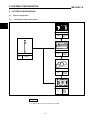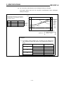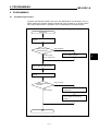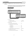
1
Digital-Analog Converter Module Type A68DAV/DAI(S1) , User s Manual MODEL A68DAV/DAI-U-E MODEL CODE 13J667 Digital-Analog Converter Module Type A68DAV/DAI(S1) , User s Manual IB(NA)-66285-D(0409)MEE HEAD OFFICE : 1-8-12, OFFICE TOWER Z 14F HARUMI CHUO-KU 104-6212,JAPAN NAGOYA WORKS : 1-14 , YADA-MINAMI 5-CHOME , HIGASHI-KU, NAGOYA , JAPAN When exported from Japan, this manual does not require application to the Ministry of Economy, Trade and Industry for service transaction permission. Specifications subject to change without notice. Mitsubishi Programmable Logic Controller SAFETY PRECAUTIONS (Always read these precautions before using this equipment.) Before using this product, please read this manual and the relevant manuals introduced in this manual carefully and pay full attention to safety to handle the product correctly. The precautions given in this manual are concerned with this product. Refer to the user's manual of the CPU module in use for details on the safety precautions for the programmable logic controller system. In this manual, the safety precautions are ranked as "DANGER" and "CAUTION". DANGER Indicates that incorrect handling may cause hazardous conditions, resulting in death or severe injury. ! CAUTION Indicates that incorrect handling may cause hazardous conditions, resulting in medium or slight personal injury or physical damage. ! Note that the ! CAUTION level may lead to a serious consequence according to the circumstances. Always follow the precautions of both levels because they are important to personal safety. Please save this manual to make it accessible when required and always forward it to the end user. [DESIGN PRECAUTIONS] ! DANGER Install a safety circuit external to the PLC that keeps the entire system safe even when there are problems with the external power supply or the PLC module. Otherwise ,trouble could result from erroneous output or erroneous operation. (1) The status of analog output changes depending on the setting of various functions that control the analog output. Take sufficient caution when setting for those functions. For details of analog output status, refer to Section 3.3.4 "Function combination". (2) If there is a fault in the output element or the internal circuit ,correct outputs may not be possible or erroneous outputs may be made. Provide a circuit to externally monitor output signals that could lead to major faults. ! CAUTION Do not bunch the control wires or communication cables with the main circuit or power wires, or install them close to each other. They should be installed 100mm (3.9inch) or more from each other. Not doing so could result in noise that would cause erroneous operation. At power ON/OFF ,voltage or current may instantaneously be output from the output terminal of this module. In such case ,wait until the analog output becomes stable to start controlling the external device. A-1 [INSTALLATION PRECAUTIONS] ! CAUTION Use the PLC in the environment that meets the general specifications given in this Manual. Using the PLC outside the range of the general specifications may result in electric shock, fire or malfunction, or may damage or degrade the module. Load the module after securely inserting the module fixing hook at the module bottom into the fixing hole of the base unit. Incorrect loading of the module can cause a malfunction , failure or drop. [WIRING PRECAUTIONS] ! CAUTION When wiring in the PLC, be sure that it is done correctly by checking the product's rated voltage and the terminal layout. Connecting a power supply that is different from the rating or incorrectly wiring the product could result in fire or damage. Tightening the terminal screws within the specified torque. If the terminal screws are loose, it could result in short circuits. fire, or erroneous operation. Tightening the terminal screws too far may cause damages to the screws or and/or the module, resulting in fallout, short circuits, or malfunction. Be sure there are no foreign substances such as sawdust or wiring debris inside the module. Such debris could cause fires, damage, or erroneous operation. [STARTING AND MAINTENANCE PRECAUTIONS] ! CAUTION Do not touch the terminals while power is on. Doing so could cause shock or erroneous operation. Be sure to shut off all phases of the external power supply used by the system before cleaning or retightening the terminal screws. Not doing so can cause the module to fail or malfunction. Do not disassemble or modify the module. Doing so could cause trouble, erroneous operation, injury, or fire. Be sure to shut off all phases of the external power supply used by the system before mounting or dismounting the module. If you do not switch off the external power supply, it will cause failure or malfunction of the module. Before handling the module, always touch grounded metal, etc. to discharge static electricity from the human body. Failure to do so can cause the module to fail or malfunction. [DISPOSAL PRECAUTIONS] ! CAUTION When disposing of this product, treat it as industrial waste. A-2 REVISIONS *The manual number is given on the bottom left of the back cover. Print Date Jul., 1991 Nov., 1997 *Manual Number IB (NA)-66285-A IB (NA)-66285-B Revision First edition Correction Section 2.2, Section 3.6, Section 4.6.2 Apr., 2001 IB (NA)-66285-C Adding models A68DA-S1 Addition WARRANTY Correction SAFETY PRECAUTIONS, Chapter 1, Section 2.2, 3.1, 3.2, 3.2.2, 3.4.1, 3.5.1, 3.6, 4.2, 4.5.2, 4.6.2, 5.2.1, 5.2.2, 5.2.3, Appendix 1 Sep., 2004 IB (NA)-66285-D Addition Conformation to the EMC Directive and Low Voltage Instruction Correction SAFETY PRECAUTIONS, Section 3.1, 3.2, 3.5.5, 4.2 Sep., 2005 IB (NA)-66285-E Correction Section 2.2, 3.2 Japanese Manual Version IB-68273-E A-3 INTRODUCTION Thank you for choosing the Mitsubishi MELSEC-A Series of General Purpose Programmable Controllers. Please read this manual carefully so that the equipment is used to its optimum. A copy of this manual should be forwarded to the end user. A-4 CONTENTS 1. INTRODUCTION ...................................................................................................................... 1 − 1 ~ 1 − 2 1.1 2. SYSTEM CONFIGURATION.................................................................................................... 2 − 1 ~ 2 − 4 2.1 3. Overall Configuration ..................................................................................................................2 − 1 2.1.1 Building block type CPU system....................................................................................2 − 1 2.1.2 Compact type CPU system............................................................................................2 − 2 2.2 Applicable A-Series Systems......................................................................................................2 − 3 2.3 Notes on Configuring the System ...............................................................................................2 − 4 SPECIFICATIONS.................................................................................................................. 3 − 1 ~ 3 − 21 3.1 General Specifications ................................................................................................................3 − 1 3.2 Performance Specifications ........................................................................................................3 − 2 3.3 3.4 3.5 3.6 4. Features ......................................................................................................................................1 − 1 3.2.1 I/O conversion characteristics of the A68DAV ...............................................................3 − 4 3.2.2 I/O conversion characteristics of the A68DAI ................................................................3 − 7 Analog Output Control Functions..............................................................................................3 − 10 3.3.1 3.3.2 Analog output HOLD/CLEAR function at STOP of CPU .............................................3 − 10 D-A conversion execute/non-execute setting function (D-A conversion output enable flag) ............................................................................3 − 10 3.3.3 Analog value external output enable/disable setting function (analog output enable/disable) ....................................................................................3 − 10 3.3.4 Function combination...................................................................................................3 − 10 CPU I/O Signal ......................................................................................................................... 3 − 11 3.4.1 Overview of I/O signals ................................................................................................ 3 − 11 3.4.2 I/O signal functions ......................................................................................................3 − 12 Buffer Memory...........................................................................................................................3 − 14 3.5.1 Buffer memory assignment ..........................................................................................3 − 14 3.5.2 Analog output enable/disable channel area (Address 0H) ...........................................3 − 15 3.5.3 CH.1 to CH.8 digital value area (Addresses 1H to 8H) .................................................3 − 15 3.5.4 Resolution setting area of digital value (Address 9H)...................................................3 − 16 3.5.5 CH.1 to CH.8 set value check code storage area (Addresses 10H to 17H) .................3 − 17 Function Block Diagram............................................................................................................3 − 17 PRE-OPERATION SETTINGS AND PROCEDURES............................................................ 4 − 1 ~ 4 − 10 4.1 Pre-operation Procedure.............................................................................................................4 − 1 4.2 Handling Instructions ..................................................................................................................4 − 2 4.3 Nomenclature..............................................................................................................................4 − 3 4.4 HOLD/CLEAR Setting of Analog Output.....................................................................................4 − 5 A-5 4.5 4.6 5. 6. Offset/Gain Setting......................................................................................................................4 − 6 4.5.1 Notes on offset/gain setting ...........................................................................................4 − 6 4.5.2 Offset/gain setting procedure.........................................................................................4 − 7 Wiring ..........................................................................................................................................4 − 8 4.6.1 Wiring instructions..........................................................................................................4 − 8 4.6.2 Connection of A68DAV/DAI/DAI-S1 and external devices ............................................4 − 8 4.6.3 Connection of connect the external power supply to the A68DAV/DAI .......................4 − 10 PROGRAMMING.................................................................................................................... 5 − 1 ~ 5 − 12 5.1 Programming Procedure.............................................................................................................5 − 1 5.2 Sample Program ........................................................................................................................5 − 2 5.2.1 Digital value setting program .........................................................................................5 − 2 5.2.2 5.2.3 Program for the A68DAV/DAI loaded in remote I/O station ..........................................5 − 4 Program for the A68DAV/DAI loaded in remote I/O station (Use of the AnACPU dedicated instruction)...................................................................5 − 9 TROUBLESHOOTING ............................................................................................................. 6 − 1 ~ 6 − 5 6.1 When the "RUN" LED Flashes or Goes OFF .............................................................................6 − 1 6.2 When the Analog Value is 0V/0 mA............................................................................................6 − 1 6.3 When Analog Values are Offset Values ......................................................................................6 − 2 6.4 Analog Values are Output though the CPU Module is set to STOP ...........................................6 − 3 6.5 When Digital and Analog Values do not Match...........................................................................6 − 4 6.6 WDT Error Flag is Set.................................................................................................................6 − 4 6.7 D-A Conversion READY Flag is Reset .......................................................................................6 − 4 6.8 Error Flag is Set ..........................................................................................................................6 − 4 APPENDICES .......................................................................................................................APP − 1 ~ APP − 4 APPENDIX 1 Comparison with Other D-A Converter Modules ..................................................... APP − 1 APPENDIX 2 Dimensions .............................................................................................................. APP − 2 2.1 A68DAV.................................................................................................................... APP − 2 2.2 A68DAI..................................................................................................................... APP − 3 A-6 Conformation to the EMC Directive and Low Voltage Instruction When incorporating the Mitsubishi PLC into other machinery or equipment and keeping compliance with the EMC and low voltage directives, refer to Chapter 3, "EMC Directives and Low Voltage Directives" of the User's Manual (Hardware) included with the CPU module or base unit used. The CE logo is printed on the rating plate on the main body of the PLC that conforms to the EMC directive and low voltage instruction. By making this product conform to the EMC directive and low voltage instruction, it is not necessary to make those steps individually. A-7 1. INTRODUCTION MELSEC-A 1. INTRODUCTION This manual describes specifications, handling, programming and other information on the A68DAV digital-to-analog converter module (referred to as "A68DAV"), the A68DAI digital-to-analog converter module (referred to as "A68DAI") and the A68DAI-S1 digital-to-analog converter module (referred to as "A68DAI-S1") for use with a MELSEC-A series CPU module. 1 (1) A68DAV Used to convert incoming digital values (16-bit signed binary data) which are set with the PLC CPU to analog values (voltage outputs ranging from -10 V to 10 V). (2) A68DAI/A68DAI-S1 Used to convert incoming digital values (16-bit signed binary data) which are set with the PLC CPU to analog values (voltage outputs ranging from 0 mA to 20 mA). In the following section, A68DAI is used generically for A68DAI and A68DAI-S1. A68DAV and A68DAI are referred to as "A68DAV/DAI" or "module" in this manual. 1.1 Features (1) Allows digital-to-analog conversion for 8 channels. The A68DAV/DAI can output analog values (voltage/current) to 8 external devices. (2) Allows setting of resolution of digital values at three stages (all channels in batch). Resolution of digital values can be set selecting from 1/4000, 1/8000 and 1/120000 by resolution setting. (3) Allows analog output to be enabled/disabled on a channel basis. Analog value output can be enabled or disabled for each channel by the sequence program. The channel disabled for analog output provides an analog output value of 0 V or 0 mA. (4) Allows setting of analog output to be held or cleared (all channels in batch) at STOP of CPU. Holding of analog output when the CPU is at STOP can be set with the HOLD/CLEAR terminal. (5) Allows offset/gain adjustment to be main without using offset/gain adjusting knobs. The offset and gain values can be specified by the UP/DOWN switch for each channel. 1−1 1. INTRODUCTION MELSEC-A MEMO 1 1−2 2. SYSTEM CONFIGURATION MELSEC-A 2. SYSTEM CONFIGURATION 2.1 2.1.1 Overall Configuration Building block type CPU system 2 CPU module Type Building block type CPU Main base unit D-A converter module Type Type A68DAV A68DAI A32B* A35B A38B Extension cable Type AC06B AC12B AC30B Extension base unit Type Fig. 2.1 Building Block REMARK 1) * An extension base cannot be connected to the A32B. 2−1 A55B A58B A65B A68B 2. SYSTEM CONFIGURATION MELSEC-A 2.1.2 Compact type CPU system 2 CPU Module Type Extension base unit D-A converter module Type A68DAV A68DAI Type A55B A58B A65B A68B Extension cable Type A0J2C04B A0J2C10B Compact type CPU I/O cable Type A0J2C01 A0J2C03 A0J2C06 I/O module Type Fig. 2.2 Compact Type CPU System Configuration 2−2 A0J2 I/O module 2. SYSTEM CONFIGURATION 2.2 MELSEC-A Applicable A-Series Systems The A68DAV/DAI can be used only for the following A-series systems. (1) The following CPU modules are suitable for A68DAV/DAI. Applicable CPU modules A0J2CPU A0J2HCPU A1NCPU A2NCPU A2NCPU-S1 A3NCPU A3HCPU A3MCPU A2ACPU A2ACPU-S1 A3ACPU A2UCPU A2UCPU-S1 A3UCPU A4UCPU A73CPU A81CPU A1CPU A2CPU A2CPU-S1 A3CPU Q2ACPU Q2ACPU-S1 Q3ACPU Q4ACPU Q4ARCPU A1SJCPU (S3) A1SJHCPU A1SCPU A1SCPUC24-R2 A1SHCPU A2SCPU A2SHCPU A2USCPU (S1) A2USHCPU-S1 Q2ASCPU (S1) Q2ASHCPU (S1) Q02CPU-A Q2HCPU-A Q06HCPU-A POINT The A68DAV/DAI cannot be used in an A0J2P25/R25(remote I/O station). (2) A68DAV/DAI may be loaded into any slot on the base unit with the following precautions: (a) When using the A68DAV/DAI with the A55B or A58B extension bases (i.e. those without power supplies), select the power supply for the main base unit in accordance with the relevant CPU module User's Manual. (b) When used with the A3CPU(P21/R21), the A68DAV/DAI cannot be loaded in the slot of the 7th extension stage in a system for which I/O allocation has been made or link X, Y defined in the parameters. (These restrictions do not apply to A3NCPU, A3HCPU, A3MCPU, A73CPU, A3ACPU). On a data link system, the A616DA can be mounted to any of the following: master station, local station or remote I/O. Refer to the MELSECNET and MELSECNET/B data link system reference manual for examples of programs for remote I/O stations. 2−3 2. SYSTEM CONFIGURATION MELSEC-A 2.3 Notes on Configuring the System (1) When using the A68DAV/DAI, an external power supply is required to supply 24 VDC to the A68DAV/DAI. When supplying a 24 VDC power, follow the power supply specifications mentioned in Section 3.2 Performance Specifications (external power supply). (refer to 4.6.3) 2−4 3. SPECIFICATIONS MELSEC-A 3. SPECIFICATIONS This chapter describes the general specifications performance specifications, and I/O conversion characteristics of the A68DAV/DAI. 3.1 General Specifications Table 3.1 shows the general specifications of the A68DAV/DAI. Table 3.1 General Specifications Item 3 Specifications Operating ambient temperature 0 to 55 °C Storage ambient temperature -20 to 75 °C Operating ambient humidity 10 to 90 %RH, non-condensing Storage ambient humidity 10 to 90 %RH, non-condensing Vibration resistance Conforming to *JIS B 3502, IEC 61132-2 Frequency Acceleration Amplitude When there is Intermittent vibration 10 to 57 Hz 0.075 mm When there is continuous vibration Shock resistance 2 57 to 150 Hz 9.8 m/s 10 to 57 Hz 0.035 mm 57 to 150 Hz 4.9 m/s2 Sweep Count 10 times each in X, Y and Z axis (80 minutes) 2 Conforming to JIS B 3502, IEC 61131-2 (147 m/s , 3 times each in 3 directions) Operating environment No corrosive gas present Operating height *3 2000 m (6582 ft) or less Installation area On the control board Over-voltage category *1 II or less Pollution rate *2 2 or less *1: Indicates the distribution area where the device is assumed to be connected, from the public power distribution network to the local machine device. Category II is applied to the devices to which the power is supplled from a fixed equipment. The surge resistance voltage of a rated 300 V device is 2500 V. *2: This is an index which indicates the occurrence rate of the conductive object in the environment where the device is used. Pollution rate II indicates that only non-conductive pollution may occur with a possibllity of generating temporary conductivity due to accidental condensation. *3: Do not operate or store the PLC in the environment where the pressure applied is equal to greater than the atmospheric pressure at the altitude of 0m. Doing so may cause a malfunction. Please consult our branch office when the PLC is to be operated under pressure. 3−1 3. SPECIFICATIONS 3.2 MELSEC-A Performance Specifications Table 3.2 shows the performance specifications of the A68DAV/DAI. Table 3.2 Performance Specifications Specifications Item A68DAV A68DAI(S1)*4 (1) 16-bit signed binary data (2) Setting range: Resolution Setting Setting Range Resolution Setting Setting Range 1/4000 1/8000 1/12000 -4000 to 4000 -8000 to 8000 -12000 to 12000 1/4000 1/8000 1/12000 0 to 4000 0 to 8000 0 to 12000 Digital input Analog output (1) 16-bit signed binary data (2) Setting range: -10 to 0 to 10 VDC (External load resistance: 2 kΩ to 1 MΩ) 0 to 20 mADC (External load resistance: 0 to 600 Ω) Digital Value Resolution I/O characteristics Digital input value 1/4000 1/8000 4000 8000 12000 +10 v 2000 4000 6000 +5 v 0 0 0 0v -2000 -4000 -6000 -5 v -4000 -8000 12000 -10 v * When offset setting is 0 V and gain setting is 10 V. Maximum 1/4000 resolution 1/8000 of analog 1/12000 value *1 Overall accuracy (accuracy to the maximum value) *2 Conversion time *3 Absolute maximum output Analog output points Insulation method Digital Value Resolution Analog 1/12000 Output Digital input value Analog 1/12000 Output 1/4000 1/8000 4000 8000 12000 +20 mA 2000 4000 6000 +12 mA 0 0 0 +4 mA * When offset setting is 4 mA and gain setting is 20 mA. 5.0 μA 2.5 mV 1.25 mV 2.5 μA 0.83 mV 1.6 μA ±1.0 % (±100 mV) ±1.0 % (±200 μA) Maximum 40 ms/8 channels (same for 1 channel) NOTE) Time from input of digital value till specified analog value (voltage/current) is output. Voltage: 0 to +12 V NOTE) A voltage or a current that exceeds these ranges is not output by an Current: 0 to +28 mA output protection ladder. 8 channels/module Photocoupler insulation between output terminals and PLC power (no insulation between channels) 32 points (I/O allocation: special function module) 38 point terminal block 0.75 to 2 mm2 (Applicable tightening torque: 39N to 59N-cm) Number of I/O points Connection terminal Applicable wire size Applicable solderless V1.25-3, V1.25-YS3A, V2-S3, V2-YS3A terminal Internal current 0.15 A consumption (5 VDC) 21.6 to 26.4 VDC External Voltage power Current 0.2 A supply consumption Weight kg (lb) 0.6 Kg 3−2 0.15 A 0.4 A 0.65 Kg 3 3. SPECIFICATIONS *1 MELSEC-A Maximum resolution of analog value The maximum resolution of analog value is the maximum variance in the analog output caused by a change in the digital value by "1". *2 Overall accuracy Over all accuracy is the accuracy to the maximum value of analog output. 1) Overall accuracy of the A68DAV is the accuracy when the output voltage setting is 10 volts. +10 V Fluctuation will be within 10V ±1% (100mV) width due to the operating environment (ambient temperature, noise). Analog output 0 V -10 V -4000 0 4000 Digital input 2) Overall accuracy of the A68DAI is the accuracy when the output voltage setting is 20 mA. 20 mA Fluctuation will be within 20mA ±1% (200μA) width due to the operating environment (ambient temperature, noise). Analog output 0 mA 0 4000 Digital input *3 Conversion speed The conversion speed is the length of time required from the reading of a digital value written to the buffer to the output of the specified analog value after D-A conversion. The conversion speed becomes the maximum when the maximum analog value output changes to the minimum analog value output, or vice versa. The maximum speed is 40 ms. *4 When using the A68DAI, passing the wire with a common cable cannot be made on the side with the external device, but it is possible with the A68DAI-SI. For details, refer to Section 4.6.2. 3−3 3. SPECIFICATIONS MELSEC-A 3.2.1 I/O conversion characteristics of the A68DAV (1) I/O conversion characteristics I/O characteristics are provided to convert a digital value specified from the CPU into an analog value and are indicated by an inclination connected between an offset value and a gain value. (2) Offset/gain values (a) The offset and gain values are defined as follows. 1) Offset value : Voltage output from the A68DAV when the digital value specified from the PLC CPU is "0". 2) Gain value : Voltage output from the A68DAV when digital value specified from the PLC CPU is "4000" (when digital value resolution setting is 1/4000). (b) Offset/gain values are set before delivery as shown below. 1) Offset value : 0 V 2) Gain value : 10 V (c) Offset/gain value can be changed for each channel in the test mode. (3) I/O conversion characteristic example The figure below shows an example of I/O conversion characteristics. Offset value (V) 15 Gain value 10 Analog output voltage 5 Practical analog output range 0 −5 −10 −15 −4000 −4096 0 * Digital input value * Digital value resolution setting is 1/4000. 4000 4095 Fig. 3.1 I/O Conversion Characteristics 3−4 3. SPECIFICATIONS MELSEC-A (4) Relation between offset/gain values and analog output Resolution of the A68DAV can be changed as appropriate by offset/gain setting. Resolution of analog value and analog output caused by digital input when offset/gain setting is changed are obtained as shown below. (Resolution of analog value) = (Analog output) = (Gain value) − (Offset value) (Resolution of digital value) (Gain value) − (Offset value) (Resolution of digital x (Digital input) + (Offset value) = (Resolution of analog value) x (Digital input) + (Offset value) The value of "resolution of digital value" (marked "*1") varies depending on the setting at buffer address "9" (digital value resolution multiplication). For the calculation, use the following values. Setting at Buffer Address "9 Value Used for Resolution of Digital Value 1 4000 2 8000 3 12000 Section 3.6 gives buffer details. POINT Due to the nature of the D-A converter of the A68DAV, the variance value of analog output values in response to an increment/decrement of the digital input value by "1" might differ from the calculated value. 3−5 3. SPECIFICATIONS MELSEC-A (5) I/O conversion characteristics when offset/gain setting is changed The figures below show the I/O conversion characteristics when offset/gain setting is changed. The right figure shows the I/O conversion characteristics when offset/gain setting is provided as follows. No. Offset Value Gain Value (1) 0V +10 V (2) −10 V +10 V (3) +4 V +8 V (V) 15 10 (3) 5 Analog output 0 voltage Practical analog output range −5 (2) (1) −10 −15 − 4096 − 4000 0 4000 4095* * Digital input * Digital value resolution setting is 1/4000. Example (1) The analog output voltages are as follows at the digital input value settings of 2000 and 500 for the characteristic graphs (1) to (3). No. (1) (2) (3) Digital Input Analog Output 2000 +5.0 V 500 +1.25 V 2000 0V 500 −7.5 V 2000 6.0 V 500 4.5 V Fig. 3.2 I/O Conversion Characteristics when Offset/Gain Setting is Changed 3−6 3. SPECIFICATIONS MELSEC-A 3.2.2 I/O conversion characteristics of the A68DAI (1) I/O conversion characteristics Since the I/O conversion characteristics are for converting the set digital values from the CPU to an analog value, they slanted by the joining of the offset value and gain value. (2) Offset/gain values (a) The offset and gain values are defined as follows. 1) Offset value : Voltage output from the A68DAI when the digital value specified from the PLC CPU is "0". 2) Gain value : Voltage output from the A68DAI when digital value specified from the PLC CPU is "4000" (when digital value resolution setting is 1/4000). (b) Offset/gain values are set before delivery as shown below. 1) Offset value : 4 mA 2) Gain value : 20 mA (c) Offset/gain value can be changed for each channel in the test mode. (3) I/O conversion characteristic example The figure below shows an example of I/O conversion characteristics. Offset value Gain value (mA) 20 15 Analog output voltage Practical analog output range 10 5 0 0 0 * Digital input value 4000 4095 Fig. 3.3 I/O Conversion Characteristics 3−7 * Digital value resolution setting is 1/4000. 3. SPECIFICATIONS MELSEC-A (4) Relation between offset/gain values and analog output Resolution of the A68DAI can be changed as appropriate by offset/gain setting. Resolution of analog value and analog output caused by digital input when offset/gain setting is changed are obtained as shown below. (Resolution of analog value)*1 = (Analog output) *1 = (Gain value) − (Offset value) (Resolution of digital value) (Gain value) − (Offset value) (Resolution of digital value) x (Digital input) + (Offset value) = (Resolution of analog value) x (Digital input) + (Offset value) The value of "resolution of digital value" (marked "*1") varies depending on the setting at buffer address "9" (digital value resolution multiplication). For the calculation, use the following values. Setting at Buffer Address "9" Value Used for Resolution of Digital Value 1 4000 2 8000 3 12000 Section 3.6 gives buffer details. POINT Due to the nature of the D-A converter of the A68DAV, the variance value of analog output values in response to an increment/decrement of the digital input value by "1" might differ from the calculated value. 3−8 3. SPECIFICATIONS MELSEC-A (5) I/O conversion characteristics when offset/gain setting is changed The figures below show the I/O conversion characteristics when offset/gain setting is changed. (mA) The right figure shows the I/O conversion characteristics when offset/gain setting is provided as follows. No. Offset Value Gain Value (1) 0 mA 20 mA (2) 4 mA 20 mA (3) 6 mA 16 mA 20 (2) 15 Practical analog output range 16 mA Analog 10 output voltage 5 (3) 6 mA (1) 4 mA 0 0 4000 * Digital input 4095 * Digital value resolution setting is 1/4000. Example (1) The analog output voltages are as follows at the digital input value settings of 2000 and 1000 for the characteristic graphs (1) to (3). No. (1) (2) (3) Digital Input Analog Output 2000 10 mA 1000 5 mA 2000 12 mA 1000 8 mA 2000 11 mA 1000 8.5 mA Fig. 3.4 I/O Conversion Characteristics when Offset/Gain Setting is Changed 3−9 3. SPECIFICATIONS MELSEC-A 3.3 3.3.1 Analog Output Control Functions Analog output HOLD/CLEAR function at STOP of CPU When the CPU is at STOP, or when the D-A conversion is stopped by the CPU module because of the occurrence of error, holding of analog output can be selected for all channels in batch with the HOLD/CLEAR terminal. 3.3.2 D-A conversion execute/non-execute setting function (D-A conversion output enable flag) This function determines if each channel outputs a D-A conversion value or an offset value by setting a D-A conversion value output enable flag for each channel in the sequence program. The D-A conversion time (conversion speed) is fixed disregarding of setting a D-A conversion value disable flag. ON : D-A conversion value OFF: offset value 3.3.3 Analog value external output enable/disable setting function (analog output enable/disable) This function determines if an analog value output to external devices is enabled or disabled by writing 0/1 to address 0 for each channel in the sequence program. Select one of the functions according to the state of the analog output to be set. 1 : 0 V/0 mA 0 : (D-A conversion value or offset value) 3.3.4 Function combination When the CPU is at RUN or STOP, or when an error occurs in the CPU, analog values can be set as shown in Table 3.3 by combining any or all of the analog output control functions. Select the most appropriate combination. Table 3.3 Analog Output State Setting Combinations Setting Combina -tion HOLD/CLEAR Setting (Section 3.3.1) CLEAR D-A Conversion Output Enable Flag (Section 3.3.2) Output Status Analog Output Enable/Disable Setting (Section 3.3.3) HOLD Enable (ON) Enable (0) Disable (OFF) Disable (1) Enable (0) Enable (ON)/Disable (OFF) Disable (1) Enable (0) Disable (1) 0 V/0 mA Analog value after D-A conversion of digital value set with the PLC CPU is output. 0 V/0 mA Analog output at CPU STOP Analog value after D-A conversion of digital value set with the PLC CPU is output. 0 V/0 mA Offset value is output. Analog output at CPU STOP Offset value is output. 0 V/0 mA Offset value is output. 0 V/0 mA Analog value before STOP is held. 0 V/0 mA Analog output at CPU error occurrence 0 V/0 mA 0 V/0 mA 0 V/0 mA 0 V/0 mA 0 V/0 mA 0 V/0 mA 3 − 10 3. SPECIFICATIONS MELSEC-A 3.4 3.4.1 CPU I/O Signal Overview of I/O signals The A68DAV/DAI uses 32 points of signals for input and output respectively. Table 3.4 gives the allocation and description of I/O signals. X devices refer to input signals from the A68DAV/DAI to the CPU. Y devices refer to output signals from the CPU to the A68DAV/DAI. The device numbers (input signals) shown in the table are used when the A68DAV/DAI is loaded into slot 0 of the main base unit. Table 3.4 I/O Singals Signal Direction: A68DAV/DAI → CPU Device No. Signal Description Signal Direction: CPU → A68DAV/DAI Device No. Signal Description X0 WDT error flag (A68DAV/DAI detection) Y0 through YC Unusable (used for system only) X1 D-A conversion READY YD through YF Interlock signal for RERP and RTOP instructions when the A68DAV/DAI is used as a remote I/O station. X2 Error flag X10 through Y17 D-A conversion value output enable flag X3 through X1C Unusable Y18 Error reset flag X1D through X1F Interlock signal for RERP and RTOP instructions when the A68DAV/DAI is used as a remote I/O station. Y19 through Y1F Unusable (used for system only) IMPORTANT Because devices Y0 through YC and Y19 through Y1F are used in the system, they cannot be used in the sequence program. If any of these devices are used (turned ON/OFF) in the sequence program, the functions of the A64DAV/DAI cannot be guaranteed. If any of the devices Y0 through Y1F, has the same number as any of the devices X0 through X1F, that device cannot be used as an internal relay. 3 − 11 3. SPECIFICATIONS MELSEC-A 3.4.2 I/O signal functions (1) WDT (watch dog timer) error flag (X0) This flag is set when the self-diagnosis function of the A68DAV/DAI detects a WDT error. While the error flag is set, the D-A conversion of the A68DAV/DAI does not RUN (0 V/0 mA is output). If the error flag (X0) is set, a hardware malfunction may occur. (2) D-A conversion READY signal (X1) This signal is turned ON when the D-A conversion is ready after turning on or resetting the CPU in a mode other than the normal mode (test mode). If the TEST terminals on the front of the module are connected to each other, this signal is turned OFF. The D-A conversion READY signal (X1) can also be used as the buffer memory read/write interlock . REMARK In this manual, "D-A conversion READY" means the time when the analog output values have been output to external equipment by executing the D-A conversion with each channel. (3) Error flag (X2) This flag is set when an error (digital value setting error) other than the watch dog timer error occurs in the A68DAV/DAI. This flag is reset when: (a) the error reset flag (Y18) is turned ON, or (b), "0" is written to the CH1 to CH8 set value check code storage areas (buffer 10 to 17). (4) Interlock signals (X1D to X1F, YD to YF) for RFRP and RTOP instructions (a) X1D and YD One of these is set when the RFRP and RTOP instructions cannot be executed because of a module error. When YD is turned ON, X1D is turned OFF. (b) X1E and YE While executing the RFRP instruction, YE is turned ON. When the execution is completed, X1E flag is turned ON and YE remains ON. Therefore, YE should be turned OFF by the sequence program. 3 − 12 3. SPECIFICATIONS MELSEC-A (c) X1F and YF While executing the RTOP instruction, YF is turned ON. When the execution is completed, X1F is turned ON and YF remains ON. Therefore, YF should be turned OFF by the sequence program. POINT Refer to the ACPU Programming Manual (Common Instructions) for the use of the interlock signals for the RFRP and RTOP instructions. (5) D-A conversion output enable flag (Y10 to Y17) If any of the D-A conversion enable flags for channels 1 to 8 are set, the D-A conversion value output of the corresponding channels is set to "enabled". If a D-A conversion value output needs to be set to "disable", reset the corresponding D-A conversion enable flag. Y10 : D-A conversion value output enable flag for channel 1 Y11 : D-A conversion value output enable flag for channel 2 Y17 : D-A conversion value output enable flag for channel 8 (6) Error reset signal (Y18) Turning ON the error reset signal (Y18) resets the error flag (X2), and clears the check code stored in the setting value check code storage area (addresses 10 to 17) of the buffer memory. It is replaced by "0". Error flag (X2) Set/Reset by the system Error reset signal (Y18) Set/Reset by the sequence program Buffer memory addresses 10 to 17 0 Check code 0 POINT The I/O allocation numbers of the A68DAV/DAI mentioned in this manual are those when the A68DAV/DAI is loaded in slot No.0 of the main base unit. 3 − 13 3. SPECIFICATIONS 3.5 MELSEC-A Buffer Memory The A68DAV/DAI has a buffer memory (not battery backed) for data communication with the CPU. The buffer memory assignment and data maps are indicated below. 3.5.1 Buffer memory assignment Address 2 (Decimal) 0 Analog output enable/ disable channel 1 CH.1 digital value 2 CH.2 digital value 3 CH.3 digital value 4 CH.4 digital value 5 CH.5 digital value 6 CH.6 digital value 7 CH.7 digital value 8 CH.8 digital value 9 Resolution of digital value 10 CH.1 set value check code 11 CH.2 set value check code 12 CH.3 set value check code 13 CH.4 set value check code 14 CH.5 set value check code 15 CH.6 set value check code 16 CH.7 set value check code 17 CH.8 set value check code Default Value Relevant Section 0000H (all channels enabled) Section 3.5.2 0 Section 3.5.3 1(1/4000) Section 3.5.4 0 Section 3.5.5 Fig. 3.5 Buffer Memory Assignment POINT Addresses 10 to 17 of the buffer memory are the read-only area. When write is executed with a sequence program, an error will occur. 3 − 14 3. SPECIFICATIONS 3.5.2 MELSEC-A Analog output enable/disable channel area (Address 0H) (1) Defines output enable/disable for the converted analog value per channel. (2) All channels are enabled for output when: (a) Power is switched on; or (b) CPU is reset. (3) Output disable/enable is defined by 1/0. (a) Disable ............... 1 (b) Enable ................ 0 (4) The analog output enable/disable channel area data map is shown below: b15 b14 b13 b12 b11 b10 b9 b8 b7 b6 b5 b4 b3 b2 b1 b0 CH. 8 CH. 7 CH. 6 CH. 5 CH. 4 CH. 3 CH. 2 CH . 1 Ignored Fig. 3.6 Analog Output Enable/Disable Channel Area Data Map 3.5.3 CH.1 to CH.8 digital value area (Addresses 1H to 8H) (1) Write digital values to this area from the CPU for D-A conversion. (2) Digital values of all channels are set to 0 if: (a) D-A conversion ready (X1) is ON after power on; or (b) D-A conversion ready (X1) is switched ON after the CPU is reset. (3) Any digital value specified should be a 16-bit signed binary within the setting range of digital value resolution. Any digital value outside this range is changed to a value indicated below before D-A conversion, and the corresponding check code is written to the set value check code area (addresses 10 to 17). 3 − 15 3. SPECIFICATIONS MELSEC-A Table 3.5 The Setting Range of Digital Value Module Digital Value Resolution Setting Range Digital Value for D-A Conversion when Values Outside the Special Ranges are Set. 1/4000 −4096 to 4095 (−4000 to 4000 : for guaranteed operation) 4096 or above : 4095 −4097 or below : −4096 1/8000 −8192 to 8191 (−8000 to 8000 :for guaranteed operation) 8192 or above : 8191 −8193 or below : −8192 1/12000 −12288 to 12287 (−12000 to 12000 : for guaranteed operation) 12288 or above : 12287 −12289 or below : −12288 1/4000 0 to 4095 (0 to 4000 : for guaranteed operation) 4096 or above : 4095 −1 or below :0 1/8000 0 to 8191 (0 to 8000 : for guaranteed operation) 8192 or above : 8191 −1 or below :0 1/12000 0 to 12287 (0 to 12000 : for guaranteed operation) 12288 or above : 12287 −1 or below :0 A68DAV A68DAI 3.5.4 Resolution setting area of digital value (Address 9H) (1) The resolution set in the resolution setting area of digital value which corresponds to the range of analog output voltage is common to all channels. (2) The resolution value of digital value is "1" (1/4000) in the following cases. (a) At power on. (b) At reset of the PLC CPU. (3) The setting value should be 1, 2 or 3. Table 3.6 Resolution Setting Range Setting Value Resolution of Digital Value 1 1/4000 2 1/8000 3 1/12000 3 − 16 3. SPECIFICATIONS MELSEC-A POINT (1) If the set value is other than 1, 2, or 3, the resolution value is not changed and is set to the last set value before set or to a default value. (2) Set the resolution multiplication value only once before the D-A conversion value output enable flag is turned ON. If the set value is changed while the D-A conversion enable flag is set, i.e. a machine is being controlled, the analog output will change causing machine control problems. 3.5.5 CH.1 to CH.8 set value check code storage area (Addresses 10H to 17H) (1) Used to check whether the set digital values are within or out of the setting range of digital value resolution. (2) The corresponding check code in Table 3.7 is stored if a digital value out of the setting range of digital value resolution is set. Table 3.7 Check Code List Check Code Description 000FH A digital value over the setting range of digital value resolution was set. 00F0H A digital value below the setting range of digital value resolution was set. 00FFH Digital values over and below the setting range of digital value resolution were set. For example, the 00FFH check code is stored if a digital value exceeding the valid range is written, and then, without the check code being reset, a digital value that falls short of the valid range is written. (3) Any check code stored once is not reset even though the corresponding set value is corrected to a valid value (within the setting range of digital value resolution). The check code should be reset by switching the error reset signal(Y18) ON. POINT The error flag(X2) is set ON to indicate that a check code has been stored to the set value check code area. 3 − 17 3. SPECIFICATIONS 3.6 MELSEC-A Function Block Diagram A68DAV X0 X1 X2 RUN LED WDT error flag Error flag Control circuit D-A conversion value Output enable flag Channel select switch OFFSET SET GAIN UP D-A conversion ready flag Offset/gain switch UP/DOWN switch DOWN Y10 to Y17 1 3 TEST 2 4 HLD/CLR OUTPUT PLC CPU module Interface with PLC CPU D-A conversion circuit Buffer memory Hold circuit +15 V −15 V GND Fig. 3.7 A68DAV Function Block Diagram 3 − 18 5 6 CH. 1 9 10 CH. 2 13 14 CH. 3 17 18 CH. 4 21 22 CH. 5 25 26 CH. 6 29 30 CH. 7 33 34 CH. 8 36 38 24 VDC 3. SPECIFICATIONS MELSEC-A A68DAI X0 X1 X2 RUN LED WDT error flag Error flag Control circuit D-A conversion value Output enable flag Channel select switch OFFSET SET GAIN UP D-A conversion ready flag Offset/gain switch UP/DOWN switch DOWN Y10 to Y17 1 3 TEST 2 4 HLD/CLR OUTPUT PLC CPU module Interface with PLC CPU Current detection circuit Current detection circuit Current detection circuit Buffer memory D-A conversion circuit Hold circuit Current detection circuit Current detection circuit Current detection circuit Current detection circuit Current detection circuit +15 V −15 V GND Fig. 3.8 A68DAI Function Block Diagram 3 − 19 5 6 CH. 1 9 10 CH. 2 13 14 CH. 3 17 18 CH. 4 21 22 CH. 5 25 26 CH. 6 29 30 CH. 7 33 34 CH. 8 24 VDC 36 38 3. SPECIFICATIONS MELSEC-A A68DAI-S1 X0 X1 X2 RUN LED WDT error flag Error flag Control circuit D-A conversion value Output enable flag Channel select switch OFFSET SET GAIN UP D-A conversion ready flag Offset/gain switch UP/DOWN switch DOWN Y10 to Y17 1 3 TEST 2 4 HLD/CLR OUTPUT PLC CPU module Interface with PLC CPU Current detection circuit Current detection circuit Current detection circuit Buffer memory Current detection circuit D-A conversion circuit Hold circuit Current detection circuit Current detection circuit Current detection circuit Current detection circuit +15 V −15 V GND Fig. 3.9 A68DAI-S1 Function Block Diagram 3 − 20 5 6 CH. 1 9 10 CH. 2 13 14 CH. 3 17 18 CH. 4 21 22 CH. 5 25 26 CH. 6 29 30 CH. 7 33 34 CH. 8 24 VDC 36 38 3. SPECIFICATIONS MELSEC-A MEMO 3 − 21 4. PRE-OPERATION SETTINGS AND PROCEDURES MELSEC-A 4. PRE-OPERATION SETTINGS AND PROCEDURES 4.1 Pre-operation Procedure Start Load module. • Load the A68DAV/DAI onto the specified slot. Connect the external power supply …..See Section 4.6.3 • Connect 24 VDC to the A68DAV/DAI for D-A conversion. 4 Specify analog output HOLD/CLEAR. ….. See Section 4.4. • Using a jumper, specify whether analog output is held or cleared at the time of CPU STOP. Offset/gain setting …..See Section 4.5 • Set the offset and gain values the channels used. Wiring …..See Section 4.6 • Connect the A68DAV/DAI and external devices. Programming, debugging …..See Section 5. • Write and check programs used for data transfer between the CPU and A68DAV/DAI. . Complete Fig. 4.1 Pre-operation Procedure 4−1 4. PRE-OPERATION SETTINGS AND PROCEDURES MELSEC-A 4.2 Handling Instructions (1) Protect the A68DAV/DAI and its terminal block from impact loads. (2) Do not remove the printed circuit boards from the housing. There are no userserviceable parts on the boards. (3) Ensure that no conductive debris can enter the module. If it does, make sure that it is removed. Guard particularly against wire offcuts. (4) Tighten the screws as specified below: Screw 4 Tightening Torque Range I/O terminal screw (M3 screw) 39 to 59 N⋅cm I/O terminal block installation screw (M4 screw) 78 to 118 N⋅cm (5) To load the module onto the base, press the module against the base so that the catch on the top of the unit is securely locked. To unload the module, push the catch, and after the catch is disengaged from the base, pull the module toward you. 4−2 4. PRE-OPERATION SETTINGS AND PROCEDURES MELSEC-A 4.3 Nomenclature (1) (2) (3) (4) (5) (6) (7) (8) No. Description Application Indicates the operating status of the A68DAV/DAI. (Normal mode) On.......................................... • Indicates that the A68DAV/DAI is operating without fault. Off.......................................... • 5 VDC is not supplied to the A68DAV/DAI. • A68DAV/DAI is in WDT error. • A68DAV/DAI hardware fault has occurred. • PLC CPU has detected an error and stopped operation. 1 "RUN" LED Flash...................................... • A write data error has occurred. (Test mode) Flash 0.5 s interval........... • OFFSET/GAIN select switch is in “OFFSET” or “GAIN” position. 0.1 s interval........... • The high or low limit of the allowed range has been exceeded ............................... during offset/gain value setting using the UP/DOWN switch. • Offset value setting is greater than gain value setting using the UP/DOWN switch. Off.......................................... • OFFSET/GAIN select switch is in “SET” position. 4−3 4. PRE-OPERATION SETTINGS AND PROCEDURES MELSEC-A No. Description Application Channel select switch CH. 2 Used to specify the channel (CH.1 to CH.8) for offset/gain adjustment. Channels should be switched when the OFFSET/GAIN select switch is in "SET" position. Only valid in test mode. (Positions "0" and "9" are ineffective.) Used to select any of the following modes: • OFFSET position : Offset value calibration mode. 3 OFFSET/GAIN select switch • GAIN position : Gain value calibration mode. • SET position : Offset/gain value storage mode. (The offset/gain value is stored to the A68DAV/DAI internal memory when the switch is moved from "OFFSET"/"GAIN" to "SET". Used to define the offset/gain value for the specified channel. Increases or decreases the offset or gain value at the following rate: 4 UP/DOWN switch • UP/DOWN position for less than 1.5 seconds : Increase or decrease spell of 0.54 mV,1.15 µA at one time. • UP/DOWN position for 1.5 seconds or more : Increase or decrease of 0.54 mV, 1.15 µA per 0.02 s. Used to select normal or test mode. 5 6 TEST mode terminals (terminal Nos. 1 and 3) Analog output HOLD/CLEAR setting terminals (terminal Nos. 2 and 4) • Disconnected : Normal mode (to output analog values to external devices) • Connected : Test mode (to set offset/gain values) Used to hold or clear analog output at the time of CPU stop. (See Section 4.4.) • Disconnected : CLEAR • Connected : HOLD Used to output an analog value after D-A conversion. 7 8 Analog output terminals (CH.1 to CH.8) Power terminals (terminal Nos. 36 and 38) Channel Terminal No. Channel Terminal No. 1 5, 6 5 21, 22 2 9, 10 6 25, 26 3 13, 14 7 29, 30 4 17, 18 8 33, 34 Input terminals for analog value output power supply (24 VDC). 4−4 4. PRE-OPERATION SETTINGS AND PROCEDURES MELSEC-A 4.4 HOLD/CLEAR Setting of Analog Output This section explains how to define a HOLD/CLEAR setting of analog output when the CPU is in the STOP mode. (1) Use the HOLD/CLEAR terminal (on the front of the A68DAV/DAI module) to define the HOLD/CLEAR setting of analog output. Table 4.1 describes the settings and their states. Table 4.1 HOLD/CLEAR Setting State of HLD/CLR Terminal (Between Terminal Nos. 2 and 4) Analog Output Setting HOLD Connected CLEAR Not connected The original(factory-set) analog output state is CLEAR(disconnected). (2) The analog output state by HOLD/CLEAR setting varies with settings of the D-A conversion value output enable flag (see Section 3.4.2) and the analog output enable/disable state (see Section 3.5.2). Table 3.3 shows the analog output states for settings of the D-A conversion value output enable flag and the analog output enable/disable state. It also shows the analog output state when the CPU is in the RUN mode. 4−5 4. PRE-OPERATION SETTINGS AND PROCEDURES MELSEC-A 4.5 Offset/Gain Setting (1) The offset and gain values are factory-set to output the voltages indicated in Table 4.2. Table 4.2 Factory-set Offset/Gain Values A68DAV A68DAI Gain value 10 V 20 mA Offset value (V) 0V 4 mA (2) The offset and gain values may be changed and fine-adjusted by offset/gain setting in test mode. 4.5.1 Notes on offset/gain setting (1) Do not select test mode during execution of D-A conversion. Selecting test mode stops D-A conversion of all channels and affects control of external devices. Returning from test mode to normal resumes D-A conversion with new offset/gain values. (2) Offset/gain setting is allowed within the following ranges: (a) A68DAV : −10 V to 0 V to + 10 V (b) A68DAI : −0 mA to 20 mA If any value set is outside the above range, overall accuracy may not be within the range of performance specifications (see Section 3.2). (3) The defined value is stored when the OFFSET/GAIN select switch is set to the "SET" position. The offset and gain value remain unchanged if test mode is terminated with the OFFSET/GAIN select switch in the "OFFSET" or "GAIN" position. (4) Before switching from one channel to another in test mode, the OFFSET/GAIN select switch should be set to the "SET" position. If the channel remains unchanged and the set value is stored to the new channel when the switch is set to "OFFSET" or "GAIN". (5) The "RUN" LED flickers fast at intervals of 0.1 seconds to indicates that the offset/gain specified has exceeded the allowed range. When the "RUN" LED is flickering fast, the offset/gain value remains unchanged if the OFFSET/GAIN select switch is set to "SET". 4−6 4. PRE-OPERATION SETTINGS AND PROCEDURES MELSEC-A 4.5.2 Offset/gain setting procedure Start Select test mode ........ "RUN" LED switched OFF. Connect the TEST terminals (terminal Nos. 1 and 3) to switch to test mode. Select channel After checking that the OFFSET/GAIN select switch is in "SET" position, set the channel select switch to the required position. Connect voltmeter Connect the voltmeter to the required channel. Select offset setting ........ "RUN" LED flashes. Move the OFFSET/GAIN select switch to "OFFSET" position. Adjust offset value Adjust the output to the offset value using the UP/DOWN switch. Define offset value ........ "RUN" LED switched OFF. Move the OFFSET/GAIN select switch to "SET" position to store offset value. Select gain setting ........ "RUN" LED flashes. Move the OFFSET/GAIN select switch to "GAIN" position. Adjust gain value Adjust the output to the gain value using the UP/DOWN switch. Define gain value ........ "RUN" LED switched OFF. Move the OFFSET/GAIN select switch to "SET" position to store the gain value. NO Channel setting complete? YES Leave test mode ........ "RUN" LED switched ON. Disconnect the TEST terminals (terminal Nos. 1 and 3) End Fig.4.2 Offset/Gain Setting Procedure 4−7 4. PRE-OPERATION SETTINGS AND PROCEDURES MELSEC-A 4.6 4.6.1 Wiring Wiring instructions Protect external wiring against noise with the following precautions: (1) Separate AC and DC wiring. (2) Separate main circuit and/or high voltage wiring from control and signal wiring. (3) Where applicable, ground the shielding of all wires to a common ground point. 4.6.2 Connection of A68DAV/DAI/DAI-S1 and external devices (1) Connection Example of A68DAV and External Devices A68DAV *1 *2 Motor driver, etc. CH. 1 2 KΩ to 1 MΩ 5 6 GND Motor driver, etc. CH. 8 2 KΩ to 1 MΩ 33 34 +15 V 35 GND 36 37 24 VDC 38 GND -15 V *1 : Use two-core shielded wiring (twisted). *2 : If noise or ripple is generated by the external wiring, connect a 0.1 to 0.47 µF (25V or more voltage resistance parts) capacitor to the input terminal of the external device. Fig. 4.3 Connection Example of A68DAV and External Devices 4−8 4. PRE-OPERATION SETTINGS AND PROCEDURES MELSEC-A (2) Connection Example of A68DAI/A68DAI-S1 and External Devices A68DAI *1 *2 Motor driver, etc. CH. 1 0Ω to 600 Ω 5 6 GND Motor driver, etc. CH. 8 0Ω to 600 Ω 33 34 +15 V 35 GND 36 37 24 VDC 38 GND -15 V *1 : Use two-core shielded wiring (twisted). *2 : If noise or ripple is generated by the external wiring, connect a 0.1 to 0.47 µF (25V or more voltage resistance parts) capacitor to the input terminal of the external device. Fig. 4.4 Connection Example of A68DAI /A68DAI-S1 and External Devices IMPORTANT (1) When using the A68DAI, never route a common jumper on the side with the external device. If wiring is not routed independently for each channel to the module as shown above, proper amperage output will not be attained. When using the A68DAI-S1, a common jumper on the side with the external device can be routed. (2) If a A68DAI-S1 inductor component load is continued, normal output may not be attained. 4−9 4. PRE-OPERATION SETTINGS AND PROCEDURES MELSEC-A 4.6.3 Connection of 24 VDC to the A68DAV/DAI The following describes the method of supplying +24 VDC to the A68DAV/DAI. (1) To connect the external power supply, twisted-wire pair cable should be used to avoid electromagnetic inductive noise. (2) When the external power supply is used, it is recommended to use noise filters with the A68DAV/DAI. Without noise filters A68DAV/DAI External power supply 36 24 VDC(+) 37 38 24 VDC(+) 0 V(-) 24 GDC(-) Twisted With noise filters A68DAV/DAI 36 24 VDC(+) 37 38 0 V(-) External power supply Twisted 24 VDC(+) Noise filter 24 GDC(-) POINT (1) The cables between the noise filters and A68DAV/DAI must not be bundled with any other cable. (2) The cables between the noise filters and A68DAV/DAI must be as short as possible. 4 − 10 5. PROGRAMMING MELSEC-A 5. PROGRAMMING 5.1 Programming Procedure Program data transfer between the CPU and A68DAV/DAI as indicated in Fig. 5.1. When utilizing the program example introduced in this chapter for an actual system, fully verify that there are no problems in the controllability of the target system. Programming Create a digital resolution setting program. Analog output disable channel specified? YES (Specified) NO (Analog output set for 8 channels) Create an analog output disable channel setting program. Create a D-A conversion value output enable flag setting program. Create a digital value write program. Defined digital value checked? NO (Not checked) YES (Checked) Create a set value check code area read program. Create a set value check code channel judgement processing program. End Fig.5.1 Programming Procedure 5−1 5 5. PROGRAMMING MELSEC-A 5.2 Sample Program This section explains the programming used with the A68DAV/DAI. IMPORTANT A FROM/TO instruction cannot be executed in the test mode. Use the D-A conversion ready signal as an interlock for any program that contains a FROM/TO instruction. If a FROM/TO instruction is executed in the test mode, the set offset and/or gain values might be lost, or a CPU error occurs. 5.2.1 Digital value setting program The following describes a program used to write a value (0 to 8000) to the digital value setting area (addresses 1 to 4 of the buffer memory) for channels 1 to 4 of the A68DAV/DAI. The value is set with a BCD digital switch. Programming conditions 5 (1) System configuration Power supply module A 3 N C P U A X 42 A Y 42 A 68 D A (V/I) (64 (64 points) points) X00 to X3F Y40 to Y7F X/Y80 to X/Y9F ................................................. I/O number (2) Initial settings (a) Digital value resolution ..................................................... "2" (1/8000) (b) Analog output disable channel ......................................... CH.5, 6, 7, 8 (3) Device for user (a) Digital value write command input signal 1) Channel No.1.............................................................. X1 2) Channel No.2.............................................................. X2 3) Channel No.3.............................................................. X3 4) Channel No.4.............................................................. X4 (b) Setting of digital value (4 digits in the BCD code)............ X30 to X3F (c) Digital value clear command ............................................ X5 (d) Digital value storage register............................................ D0 5−2 5. PROGRAMMING MELSEC-A Programming Procedure WDT error flag D-A conversion ready flag X080 X081 M9038 Initial setting 0 TOP H0008 K9 K2 K1 ........ TOP H0008 K0 H00F0 K1 ........ Y090 Setting the D-A conversion value output enable flag Y091 Y092 BINP 27 K4X030 D0 ........ PLS M0 ......... X002 Reading digital values and checking if a read value is within the settable range <= D0 K8000 X003 X004 M0 TOP H0008 K1 D0 K1 TOP H0008 K2 D0 K1 TOP H0008 K3 D0 K1 TOP H0008 K4 D0 K1 TOP H0008 K1 K0 K4 X002 X003 X004 X005 Clearing the digital values of each channel End Inputs (X30 to X3F) from BCD digital switches are converted into binary values and put into D0. M0 is turned ON for one scan when the D0 value is within the allowable range (D0 ≤ 8000). X001 44 Writing the digital value Channels 5 to 8 are set as the analog output disabled channel. The D-A conversion value ....... output enable flag for channels 1 to 4 is turned ON. Y093 X001 Resolution multiplication value is set to "2" (1/8000). 89 When M0 is ON, the value in D0 is written to the digital value storage ....... area of the channel for which the digital value write command is ON. ......... When the digital value clear command is turned ON, "0" is written to buffer add CIRCUIT END POINT During each of the processes of the special function module, access from the PLC CPU will have priority. Accordingly, if frequent access to the buffer memory of the special function module made from the PLC CPU, it will not only extend the scan time of the PLC CPU, delays in each of the processes of the special function module will occur. Only use the FROM/TO and other such commands to access the buffer memory from the PLC CPU when necessary. 5−3 5. PROGRAMMING MELSEC-A 5.2.2 Program for the A68DAV/DAI loaded in remote I/O station The following program is used to write a value (0 to 8000) defined by the BCD digital switch to channels 1 to 4 (addresses 1 to 4 of buffer memory) of the A68DAV/DAI in a remote I/O station. Cautions on programming (1) Data transfer method The CPU has direct and refresh I/O control modes. Data transfer between the CPU and remote I/O station is made in batch refresh mode after execution of the END (FEND) instruction. (2) Response delay A time difference (response delay) occurs because control data transferred between the master station CPU and remote I/O station A68DAV/DAI is controlled through the link module. Control timing must therefore be noted. (3) Instructions used The following instructions are used for data transfer between the master station CPU and remote I/O station A68DAV/DAI. (a) Data write (master station to A68DAV/DAI) : RTOP instruction (b) Data read (A68DAV/DAI to master station) : RFRP instruction (4) Device for data transfer Link registers (W) are used for data transfer between the master station CPU and remote I/O station A68DAV/DAI. Write either of both of the following programs to the master station as appropriate: (a) Data write : Program which transfers data (to be transferred to the remote I/O station A68DAV/DAI) to the specified link registers before execution of the RTOP instruction. (b) Data read : Program which transfers data from the link registers to the other device after execution of the RFRP instruction. (5) Disable simultaneous execution of RTOP and RFRP instructions The RTOP ad RFRP instructions cannot be executed at the same time to one A68DAV/DAI. To enable simultaneous execution, data link I/O signals must be written in the program as interlock conditions. (When two A68DAV/DAI are loaded in the remote I/O station, the RTOP instruction may be executed to one A68DAV/DAI and the RFRP instruction to the other at the same time.) 5−4 5. PROGRAMMING MELSEC-A (6) Control signals to the A68DAV/DAI Because of the relation between the master station scan time and link scan time, the PLS Y[ ][ ] signal output to the remote I/O station may not be provided to the A68DAV/DAI. The pulse output which executes the RST instruction after the SET instruction cannot be used because data is transferred between the master station and remote I/O station in batch refresh mode after execution of the END (FEND) instruction. (7) Detection of remote I/O station error or parameter communication (a) Provide interlock using the following devices so that the RTOP/RFRP instruction is not executed when the remote I/O station is faulty or during initial communication with the remote I/O station. 1) Remote I/O station error detection : D9228 to D9231 2) Initial communication detection : D9224 to D9227 The remote I/O station error and initial communication detection timings are as shown below: Error detection Initial communication RTOP/RFRP instruction disabled (b) The error detection program must communication detection program. be written before the initial If these programs are written in reverse order, neither error nor initial communication may be detected depending on the link refresh timing. (8) A68DAV/DAI error detection (a) X1D is switched ON to indicate that the A68DAV/DAI is faulty and the RFRP/RTOP instruction cannot be executed. In this case, check the A68DAV/DAI for A68DAV/DAI fault, module loading error, etc. (b) Switch ON YD to switch OFF X1D YD must only be switched ON/OFF as described below by using the SET/RST instruction: 1) Switched ON when X1D is switched ON. 2) Switched OFF only once when X1D is switched OFF. 5−5 5. PROGRAMMING MELSEC-A Programming condition (1) System configuration Master station Power supply module A 3 N C P U P 21 A X 42 A Y 42 64 64 points points X0 to X3F Y40 to Y7F Remote I/O station No.1 Power supply module A J 72 P 25 A 68 D A (V/I) X/Y200 to X/Y21F ....... Allocation of I/O number in the master station (2) Initial settings (a) Digital value resolution ..................................................... "2" (1/8000) (b) Analog output disable channel ......................................... CH.5, 6, 7, 8 (3) Device for user (a) Initial setting command input signal ................................. X0 (b) Digital value write command input signal 1) Channel No.1.............................................................. X1 2) Channel No.2.............................................................. X2 3) Channel No.3.............................................................. X3 4) Channel No.4.............................................................. X4 (c) Setting of digital value (4 digits in the BCD code )........... X30 to X3F (d) Digital value clear command ............................................ X5 (e) Start/completion signal of each processing ..................... M0 to M16 (f) Data storage register at an error detection ...................... D0, D1 (g) Initial setting data register 1) Resolution value register ............................................ W101 2) Analog output enable/disable channel setting data register ...................................... W102 (h) Digital value register 1) Channel No.1.............................................................. W111 2) Channel No.2.............................................................. W112 5−6 5. PROGRAMMING MELSEC-A 3) Channel No.3.............................................................. W113 4) Channel No.4.............................................................. W114 Programming Procedure M9036 0 Detection of a remote I/O station error M0 <> K0 D0 <> Y20E K0 D1 WAND H0001 D9228 D0 WAND H0001 D9224 D1 M0 27 RST Y20E RST Y20F N0 M1 PLS M2 SET M3 PLS M4 Y20F M0 34 N0 MC M1 X1000 M10 40 M2 45 Y20E X21E Y20F X21F M3 47 M3 M5 M4 59 Detection of an error in remote I/O station 1 (Error detected if bit 0 of ........... D9228 is "1") Detection of parameter communications with remote ........... I/O station 1 (Initial data communications ON if bit 0 of D9224 is "1") ........... M0 is turned ON if it is in the initial data communications state, or if a remote I/O station 1 error is detected. The RFRP and RTOP ...... instruction handshake signals are reset when M0 is turned ON. ........... The MC instruction is turned ON when communications with remote I/O station 1 is successful. When the initial setting has not been completed (M10 ...... is OFF), M3 goes ON if the initial setting execution command is turned ON. ....... The signal is converted into pulses when the initial setting is executed. In other cases, M5 is turned ON. (M5 is used as the execution enable flag for RFRP and RTOP instructions) RST M3 RST M7 RST M8 RST M9 RST M12 RST M13 RST M14 RST M15 RST M16 SET M6 ........... multiplication value setting K2 W101 Initial setting data is ....... set to the M → R link register. The execution completed ....... flag of each process is reset. The resolution MOV Setting initial setting data MOV H00F0 W102 instruction is turned ON. M6 RTOP H0200 80 K9 W101 K1 RST M6 RST Y20F SET M7 PLS M8 RST M7 SET M9 X21F Writing a resolution multiplication value X21D M7 The resolution ...... multiplication value (the data in W101) is written to buffer address 9. M5 98 M9 is turned ON after the M8 1 104 5−7 ....... completion of the resolution multiplication value setting. 5. PROGRAMMING MELSEC-A 1 M9 RTOP H0200 106 K0 W102 K1 RST M9 RST Y20F SET M10 X21F Analog output enable/disable setting Channels 5 to 8 are set ....... to the analog output disabled channel. X21D M10 is turned ON at the .......... completion of the initial setting. M10 X200 X201 124 Y210 Y211 Setting the D-A conversion value output enable flag Y212 Y213 After the completion of the initial setting, the D-A conversion value output ....... enable flag is set if the WDT error flag is turned OFF and the D-A conversion ready flag is turned ON. X001 BINP K4X030 D10 X002 Reading digital values and checking if the read value is within the settable range <= D10 PLS M11 MOV D10 W111 MOV D10 W112 MOV D10 W113 MOV D10 W114 SET M12 PLS M13 RST M12 SET M14 W111 K4 RST M14 RST Y20F PLS M15 W115 K4 SET M16 W115 K4 RST M16 RST Y20F MCR N0 K8000 X003 X004 M11 Inputs (X30 to X3F) from BCD digital switches are converted into binary ....... values and stored in D10. M11 is turned ON for one scan when the D10 value is within the allowable range (D10 â 8000). X001 151 X002 Transmitting read digital values to the link register X003 Data in D10 is ....... transmitted to the link register. X004 M12 is turned ON after M12 ........... the completion of transmission. M5 182 M13 188 After the completion of transmission, the digital value write command ....... (M14) goes ON if the RFRP and RTOP instructions have not been executed. M14 190 RTOP H0200 K1 X21F Writing digital values X21D X005 FMOVP K0 M15 221 If the RFRP and RTOP instructions have not been executed with the ....... digital value clear command ON, "0" is stored in W115 to W118 and M16 is turned ON. M16 223 RTOP H0200 K1 X21F Data in W115 to W118 is X21D 240 End Data in W111 to W114 is written to buffer addresses 1 to 4. M5 207 Clearing the digital values of each channel ....... CIRCUIT END 5−8 ....... written to buffer addresses 1 to 4 when M16 is turned ON. .......... MC instruction is reset. 5. PROGRAMMING MELSEC-A 5.2.3 Program for the A68DAV/DAI loaded in remote I/O station (Use of the AnACPU dedicated instruction) The following program is used to write a value (0 to 8000) defined by the BCD digital switch to channels 1 to 4 (addresses 1 to 4 of buffer memory) of the A68DAV/DAI in a remote I/O station when AnACPU dedicated instructions are used. Programming condition (1) System configuration Master station Power supply module A 3 A C P U P 21 A X 42 A Y 42 64 64 points points X0 to X3F Y40 to Y7F Remote I/O station No.1 Power supply module A J 72 P 25 A 68 D A (V/I) X/Y200 to X/Y21F ...... Allocation of I/O number in the master station (2) Initial settings (a) Digital value resolution ..................................................... "2" (1/8000) (b) Analog output disable channel ......................................... CH.5, 6, 7, 8 (3) Device for user (a) Initial setting command input signal ................................. X0 (b) Digital value write command input signal 1) Channel No.1.............................................................. X1 2) Channel No.2.............................................................. X2 3) Channel No.3.............................................................. X3 4) Channel No.4.............................................................. X4 (c) Setting of digital value (4-digit in the BCD code ) ............ X30 to X3F (d) Digital value clear command ............................................ X5 (e) Start/completion signal of each program ......................... M0 to M9 5−9 5. PROGRAMMING MELSEC-A (f) Initial setting data storage link register 1) Resolution value register ............................................ W101 2) Analog output enable/disable channel setting data register ...................................... W102 (g) Digital value read data register ........................................ D0 (h) Digital value storage link register 1) Channel No.1.............................................................. W111 2) Channel No.2.............................................................. W112 3) Channel No.3.............................................................. W113 4) Channel No.4.............................................................. W114 5 − 10 5. PROGRAMMING MELSEC-A Programming Procedure X000 MOV H00F0 W102 When initial setting has not been completed (M5 is OFF), M0 is goes ON if ...... the initial setting execution command is turned ON. Initial setting data is set .... to the M → R link register. SET ...... completion of the setting M5 0 PLS M0 K2 W101 M0 Setting initial data MOV 5 M1 is turned ON after the M1 M1 17 of initial setting data. LEDB RTOP SUB H0200 SUB K9 The resolution Writing a resolution multiplication value LEDC W101 value (the .... multiplication data in W101) is written to buffer address 9. SUB K1 LEDC M2 LEDR M2 47 SET M3 RST M1 M3 50 M3 is turned ON after the completion of the setting .... of the resolution multiplication value (the data in W101). LEDB RTOP SUB H0200 SUB Analog output enable/disable setting K0 LEDC W102 SUB K1 LEDC M4 Channels 5 to 8 are set .... to the analog output disabled channel. LEDR M4 80 M5 SET M5 RST M3 Y210 Y211 Setting D-A conversion value output enable flag Y212 Y213 X001 BINP K4X030 D0 X002 <= D0 K8000 PLS M0 MOV D0 W111 MOV D0 W112 MOV D0 W113 MOV D0 W114 SET M7 X003 X004 M6 setting. X200 X201 83 Reading digital values and checking if the read value is within the settable range M5 is turned ON at the .... completion of the initial After the completion of the initial setting, the D-A conversion value output .... enable flag goes ON if the WDT error flag is turned OFF and the D-A conversion ready flag is turned ON. Inputs (X30 to X3F) from BCD digital switches are converted into binary values and .... stored in D0. M6 is turned ON for one scan the when D0 value is within the allowable range (D0 ≤ 8000). X001 110 X002 Transmitting read digital values to the link register X003 .... Data in D0 is transmitted to the link register. X004 M7 is turned ON after the 1 5 − 11 ...... completion of transmission. 5. PROGRAMMING MELSEC-A 1 M7 141 LEDB RTOP SUB H0200 SUB K1 Data in W111 to W114 is Writing digital values LEDC W111 SUB K4 LEDC M8 .... written to buffer addresses 1 to 4. LEDR M8 M7 is reset after the 171 RST M7 W115 K4 X005 173 FMOVP K0 ....... completion of the writing of digital values. LEDB RTOP SUB H0200 SUB Clearing the digital values of each channel K1 LEDC W115 SUB K4 LEDC M9 LEDR End CIRCUIT END 5 − 12 "0" is stored in W115 to W118 when the digital .... value clear command is turned ON and the data in W115 to W118 is written to buffer addresses 1 to 4. 6. TROUBLESHOOTING MELSEC-A 6. TROUBLESHOOTING Problem conditions and troubleshooting diagnoses for the A68DAV/DAI are given below. For information on the CPU module, see the corresponding CPU User's Manual. 6.1 When the RUN LED Flashes or Goes OFF (1) When the RUN LED goes OFF: Items to Check Corrective Actions Are the TEST terminals shorted? (Test mode) Cancel the test mode by opening the TEST terminals. Has an error occurred in the CPU module? Refer to the appropriate User's Manual for error information, and correct the error Is the power supply module (5 VDC) installed to the base unit not getting enough current? Recalculate the total amperage for the CPU, I/O module, and special function module installed to the base unit, and replace the power supply module based on that calculation. Is the A68DAV/DAI WDT error flag set? Reset the CPU module. (2) When the RUN LED flashes: Items to Check Corrective Actions Has a digital value outside the set range been written? Clear the set value check code storage area using the error reset flag. Are the TEST terminals closed (test mode) with the offset/gain switch placed in either "OFFSET" or "GAIN"? After setting the offset or gain value, open the TEST terminals. Does the LED flash at 0.1 s intervals when in the test mode? Make offset/gain setting within an allowable range. 6.2 When the Analog Value is 0 V/0 mA (1) When the values of all channels are 0 V/0 mA: Items to Check Corrective Actions Is the RUN LED of the A68DAV/DAI turned OFF? Follow procedures in Section 6.1. Is the WDT error flag set? Follow procedures in Section 6.7. Is the D-A conversion ready flag set? Follow procedures in Section 6.8. Is the channel set as the analog output enabled/disabled channel? Set the channel to be used as the analog output enabled/disabled channel. Is a digital value written to the digital value setting area (addresses 1 to 8) in the buffer? Write the digital value to the channel used for D-A conversion (see Sections 3.5.3 and 5.2.). 6−1 6 6. TROUBLESHOOTING MELSEC-A (2) When the value of a given channel is 0 V/0 mA: Items to Check Corrective Actions Is the analog output enable/disable channel with its "0 V/0 mA" analog value set to disable? Confirm the data set in the analog output enable/disable channel setting area of the buffer memory. (Refer to Section 3.5.2.) Is the digital value of the channel with its "0 V/0 mA" analog value written in the digital value setting area of the buffer memory? Write the digital value. (Refer to Section 3.5.3.) Is the external wiring done correctly? Make sure the external wiring is correct. 6.3 When Analog Values are Offset Values (1) When the analog values of all channels are offset values: Items to Check Corrective Actions Are the TEST terminals shorted? (Test mode) Cancel the test mode by opening the TEST terminals. Is the RUN key switch of the CPU module set to a position other than "RUN"? Set the switch to the RUN position Is the D-A conversion output enable flag of each channel OFF? Turn ON the D-A conversion output enable flag of the channel to be used. Is the digital value setting area (addresses 1 to 8) of the buffer memory? Write the digital values of the channel to be converted from digital to analog. (Refer to Sections 3.5.3 and 5.2 ) (2) When the analog value of a given channel is an offset value: 6 Items to Check Corrective Actions Is the D-A conversion output enable flag OFF for the channel when the analog value is an offset value? Turn ON the D-A conversion output enable flag. Is the digital value of the channel whose analog value is an offset value written to the digital value setting area of the buffer memory? Write the digital value. (Refer to Section 3.5.3.) 6−2 6. TROUBLESHOOTING MELSEC-A 6.4 Analog Values are Output though the CPU Module is set to STOP (1) When the analog output does not change after setting to STOP: Items to Check Are the HOLD/CLEAR setting terminals shorted(held)? Corrective Actions Open the HOLD/CLEAR setting terminals. (2) When the analog output changes after setting to STOP: Items to Check Is the analog output set to offset value? Corrective Actions After checking the offset value setting, set the offset value again if 0 V/0 mA output is required. 6−3 6. TROUBLESHOOTING MELSEC-A 6.5 When Digital and Analog Values do not Match (1) When both digital values and analog values change: Items to Check Corrective Actions Does the digital value match the analog value? Correct the offset/gain values. Are the A68DAV/A68DAI and external devices properly wired? Make sure the wiring between the A68DAV/A68DAI and the external devices is correct. Is the 24 VDC external power supply getting enough current? Recalculate the total amperage for the module installed to the base unit, and replace the power supply module based on that calculation. (2) When the digital value changes and the analog value is fixed: Items to Check Corrective Actions Is 24 VDC power being supplied? Check the external power supply. Is the RUN key switch of the CPU module set to a position other than "RUN"? Set the switch to the RUN position. 6.6 WDT Error Flag is Set Item to Check Corrective Actions Is the WDT setting time shorter than the sequence program scan time? Change the WDT setting time to conform to the sequence program scan time. Is the sequence program correct? Check if the sequence program contains an infinite loop. 6.7 D-A Conversion READY Flag is Reset Items to Check Corrective Actions Are the TEST terminals closed (test mode)? Cancel test mode by opening the TEST terminals. Is there an error in the CPU module? See the corresponding User's Manual for respective CPU module for error information. Correct the error. Is there an I/O number error? Confirm and correct the I/O number. 6.8 Error Flag is Set Item to Check Is a value that is not "0" set in the setting value check code storage area (addresses 10 to 17) of the buffer memory? Corrective Action Find out why a digital value outside the set range is written to the digital value setting area of the channel that corresponds to the non-zero set value check code storage area. Then, take corrective action and use the error reset flag to clear the set value check code storage area. 6−4 6. TROUBLESHOOTING MELSEC-A POINT If all of the troubleshooting checks do not show problems, or if the prescriped corrective measures do not solve the problem, the A68DAV/DAI hardware might be faulty. Consult a Mitsubishi representative. 6−5 APPENDICES MELSEC-A APPENDICES APPENDIX 1 Comparison with Other D-A Converter Modules Table 1.1 shows the comparison of A68DAV/DAI and other D-A converter modules. Table 1.1 Comparison List Specifications Item A62DA Voltage ±2000 Digital input *2 *1 A616DAV/A616DAI *1 A68DAV/A68DAI −4000 to 4000 Maximum -12000 to 12000 (Varies according to resolution setting) 0 to +4000 Current ±1000 0 to 4000 Maximum 0 to 12000 (Varies according to resolution setting) Voltage −10 to 0 to +10 VDC (External load resistance : 500 Ω to 1 MΩ) −10 to 0 to 10 VDC/ −5 to 0 to 5 VDC (External load resistance: 2 KΩ to 1 MΩ) −10 to 0 to 10 VDC (External load resistance: 2 KΩ to 1 MΩ) Current −20 to 0 to 20 mADC (External load resistance: 0 Ω to 600 Ω) 0 to 20 mADC (External load resistance: 0 Ω to 600 Ω) 0 to 20 mADC (External load resistance: 0 Ω to 600 Ω) Voltage 5 mV (1/2000) 1 to 5 V :1 mV (1/4000) 0 to 5 V :1.25 mV (1/4000) 0 to 10 V :2.5 mV (1/4000) −10 to 0 to 10 V : 1.30 mV (1/4000) −5 to 0 to 5 V : 0.65 mV (1/4000) 2.5 mV (1/4000) 1.25 mV (1/8000) Selec0.83 mV (1/12000) table Current 20 µA (1/1000) 4 to 20 mA : 4 µA (1/4000) 0 to 20 mA : 5 µA (1/4000) 2.64 µA (1/4000) 5 µA (1/4000) 2.5 µA (1/8000) 1.6 µA (1/12000) Analog output Maximum resolution App A62DA-S1 Selectable Overall accuracy (Precision related to the maximum value) Within ±1.0% Within ±0.6% Within ±1.0% Number of channels of analog output 2 channels/module 16 channels/module 8 channels/module Conversion time Within 15 ms/2 channels (same with 1 channel) 0.5 ms/channel Within 40 ms/8channels (same with 1 channel) Voltage ±12 V 0 to 12 V ±12 V ±12 V Current ±28 mA 0 to 28 mA Absolute maximum output Conversion method 2-channel simultaneous scanning Offset/Gain adjustment Adjustable without using offset/gain adjusting knobs Insulation method Between input terminal and PLC Photocoupler insulation Between channels Not insulated Output HOLD/CLEAR setting at STOP of PLC Disabled Channel designation of D-A conversion Batch designation of all channels with output enable flag Designation of D-A conversion enable/disable with output enable flag Batch designation of all channels Voltage External power supply Current 0 to 28 mA 0 to 28 mA Scanning by each channel 8 channels simultaneous scan method Enabled Designation by each channel 24 VDC 0.35 A *1 *2 Designation by each channel by setting of analog output enable/disable channel ±15 VDC 24 VDC +15 V:0.2 A, −15 V:0.17 A (DAV) 0.2 A (DAV) +15 V:0.53 A, −15 V: 0.125 A (DAI) 0.4 A (DAI) In the columns of the A616DAV/A616DAI and A68DAV/A68DAI where the voltage and current areas are shown, values in the voltage area indicate specification of the voltage converter module (A[ ]DAV), and those in the current area indicate specification of the current converter module (A[ ]DAI). Digital input values that allow the analog output value of a practicable range to be obtained are specified. APP − 1 APPENDICES MELSEC-A APPENDIX 2 Dimensions 2.1 A68DAV 4.2 (0.17) M3×0.5×6 2 (0.08) (Terminal screw) 8.6 (0.34) Printer circuit board 250 (9.84) App 7.2 (0.28) 6 (0.24) 4.2 (0.17) 106 (4.17) 10 (0.39) 18 (0.71) 25 (0.98) 131 (5.16) 37.5 (1.48) Unit : mm (in) APP − 2 APPENDICES MELSEC-A 2.2 A68DAI 4.2 (0.17) M3×0.5×6 2 (0.08) (Terminal screw) 8.6 (0.34) Printer circuit board 250 (9.84) 7.2 (0.28) 6 (0.24) 4.2 (0.17) 106 (4.17) 10 (0.39) 18 (0.71) 25 (0.98) 131 (5.16) 37.5 (1.48) Unit : mm (in) APP − 3 APPENDICES MELSEC-A MEMO APP − 4 WARRANTY Please confirm the following product warranty details before using this product. 1. Gratis Warranty Term and Gratis Warranty Range If any faults or defects (hereinafter "Failure") found to be the responsibility of Mitsubishi occurs during use of the product within the gratis warranty term, the product shall be repaired at no cost via the sales representative or Mitsubishi Service Company. However, if repairs are required onsite at domestic or overseas location, expenses to send an engineer will be solely at the customer’s discretion. Mitsubishi shall not be held responsible for any re-commissioning, maintenance, or testing onsite that involves replacement of the failed module. [Gratis Warranty Term] The gratis warranty term of the product shall be for one year after the date of purchase or delivery to a designated place. Note that after manufacture and shipment from Mitsubishi, the maximum distribution period shall be six (6) months, and the longest gratis warranty term after manufacturing shall be eighteen (18) months. The gratis warranty term of repair parts shall not exceed the gratis warranty term before repairs. [Gratis Warranty Range] (1) The range shall be limited to normal use within the usage state, usage methods and usage environment, etc., which follow the conditions and precautions, etc., given in the instruction manual, user's manual and caution labels on the product. (2) Even within the gratis warranty term, repairs shall be charged for in the following cases. 1. Failure occurring from inappropriate storage or handling, carelessness or negligence by the user. Failure caused by the user's hardware or software design. 2. Failure caused by unapproved modifications, etc., to the product by the user. 3. When the Mitsubishi product is assembled into a user's device, Failure that could have been avoided if functions or structures, judged as necessary in the legal safety measures the user's device is subject to or as necessary by industry standards, had been provided. 4. Failure that could have been avoided if consumable parts (battery, backlight, fuse, etc.) designated in the instruction manual had been correctly serviced or replaced. 5. Failure caused by external irresistible forces such as fires or abnormal voltages, and Failure caused by force majeure such as earthquakes, lightning, wind and water damage. 6. Failure caused by reasons unpredictable by scientific technology standards at time of shipment from Mitsubishi. 7. Any other failure found not to be the responsibility of Mitsubishi or that admitted not to be so by the user. 2. Onerous repair term after discontinuation of production (1) Mitsubishi shall accept onerous product repairs for seven (7) years after production of the product is discontinued. Discontinuation of production shall be notified with Mitsubishi Technical Bulletins, etc. (2) Product supply (including repair parts) is not available after production is discontinued. 3. Overseas service Overseas, repairs shall be accepted by Mitsubishi's local overseas FA Center. Note that the repair conditions at each FA Center may differ. 4. Exclusion of loss in opportunity and secondary loss from warranty liability Regardless of the gratis warranty term, Mitsubishi shall not be liable for compensation of damages caused by any cause found not to be the responsibility of Mitsubishi, loss in opportunity, lost profits incurred to the user by Failures of Mitsubishi products, special damages and secondary damages whether foreseeable or not , compensation for accidents, and compensation for damages to products other than Mitsubishi products, replacement by the user, maintenance of on-site equipment, start-up test run and other tasks. 5. Changes in product specifications The specifications given in the catalogs, manuals or technical documents are subject to change without prior notice. 6. Product application (1) In using the Mitsubishi MELSEC programmable logic controller, the usage conditions shall be that the application will not lead to a major accident even if any problem or fault should occur in the programmable logic controller device, and that backup and fail-safe functions are systematically provided outside of the device for any problem or fault. (2) The Mitsubishi programmable logic controller has been designed and manufactured for applications in general industries, etc. Thus, applications in which the public could be affected such as in nuclear power plants and other power plants operated by respective power companies, and applications in which a special quality assurance system is required, such as for Railway companies or Public service purposes shall be excluded from the programmable logic controller applications. In addition, applications in which human life or property that could be greatly affected, such as in aircraft, medical applications, incineration and fuel devices, manned transportation, equipment for recreation and amusement, and safety devices, shall also be excluded from the programmable logic controller range of applications. However, in certain cases, some applications may be possible, providing the user consults their local Mitsubishi representative outlining the special requirements of the project, and providing that all parties concerned agree to the special circumstances, solely at the users discretion. Digital-Analog Converter Module Type A68DAV/DAI(S1) , User s Manual MODEL A68DAV/DAI-U-E MODEL CODE 13J667 Digital-Analog Converter Module Type A68DAV/DAI(S1) , User s Manual IB(NA)-66285-E(0509)MEE HEAD OFFICE : TOKYO BUILDING, 2-7-3 MARUNOUCHI, CHIYODA-KU, TOKYO 100-8310, JAPAN NAGOYA WORKS : 1-14 , YADA-MINAMI 5-CHOME , HIGASHI-KU, NAGOYA , JAPAN When exported from Japan, this manual does not require application to the Ministry of Economy, Trade and Industry for service transaction permission. Specifications subject to change without notice. Mitsubishi Programmable Logic Controller