1
intet
Pentium® Processor
Specification Update
Release Date: March, 1995
Order Number: 242480-002
Information is this document is provided in connection with Intel products. Intel assumes no liability whatsoever, including
infringement of any patent or copyright, for sale and use of Intel products except as provided in Intel's Terms and Conditions of
Sale for such products.
Intel retains the right to make changes to these specifications at any time, without notice.
Contact your local Intel sales office or your distributor to obtain the latest specifications before placing your product order.
MDS is an ordering code only and is not used as a product name or trademark of Intel Corporation.
'Other brands and names are the property of their respective owners.
tSince publication of documents referenced in this document, registration of the Pentium, OverDrive, and iCOMP trademarks
has been issued to Intel Corporation.
Copies of documents which have an ordering number and are referenced in this document, or other Intel literature, may be
obtained from:
Intel Corporation
P.O. Box 7641
Mt. Prospect, IL 60056-7641
or call 1-800-879-4683
®INTEL CORPORATION 1995
intaL
PENTIUM@ PROCESSOR SPECIFICATION UPDATE
CONTENTS
REVISION HISTORY ...............................................................................................................................................v
PREFACE ................................................................................................................................................................ vii
Part I: Specification Updates for 60- and 66-MHz Pentium@ Processors
GENERAL INFORMATION ......................................................................................................................................3
SPECIFICATION CHANGES ..................................................................................................................................8
ERRATA .................................................................................................................................................................13
SPECIFICATION CLARIFICATIONS ....................................................................................................................27
DOCUMENTATION CHANGES ............................................................................................................................32.
Part II: Specification Updates for 75-, 90- and 100-MHz Pentium@ Processors
GENERAL INFORMATION ....................................................................................................................................39
SPECIFICATION CHANGES ................................................................................................................................42
ERRATA .................................................................................................................................................................49
SPECIFICATION CLARIFICATIONS ....................................................................................................................86
DOCUMENTATION CHANGES ............................................................................................................................91
iii
PENTIUM~ PROCESSOR SPECIFICATION UPDATE
REVISION HISTORY
Date of Revision
February 1995
Version
Description
-001
This document consolidates information previously contained in
C and D
various versions of stepping information, notably the
stepping of Pentium® Processor at iCOMP® Index (510\60, 567\66)
and the and C stepping of Pentium Processor at iCOMP Index
(610\75,735\90,815\100).
e,
e
March 1995
-002
Added Errata 22-25 and Spec Clarification 15 to Part I. Added Spec
Change 12, Errata 24-27, 8DP-12DP and 11AP, Spec Clarification
3, and Doc Change 6 to Part Ii.
v
inteL
PENTIUM® PROCESSOR SPECIFICATION UPDATE
PREFACE
This document is an update to the specifications contained in the Pentium™ Family User's Manual. It is intended
for hardware system manufacturers and software developers of applications, operating systems, or tools. It
contains Specification Changes, Errata, Specification Clarifications, and Documentation Changes, and is divided
into the following two parts:
Part I:
Specification Update for 60- and 66-MHz Pentium processors
Part II:
Specification Update for 75-, 90-, and 100-MHz Pentium processors
Contact Information
For questions or comments, please call one of the following numbers:
DIRECT NUMBERS
US and Canada
US (from overseas)
Australia
England
France
Germany
Hong Kong
India
Japan
Korea
People's Republic of China
Singapore
Taiwan
1-800-628-8686
1-91 6-356-3551
61-2-975-3300
+44 (0) 1793431144
+44 (0) 1793 421777
+44 (0) 1793 421333
852-844-4555
91-80-2215065
0120-868686
82-2-767-2500
86-1-505-0386
65-735-3811
886-2-514-4200
vii
PENTIUM@ PROCESSOR SPECIFICATION UPDATE
Nomenclature
Specification Changes are modifications to the generally available specification of the Pentium processor.
These modifications will be reflected in the Pentium™ Family User's Manual.
Errata describe any problems associated with the current stepping of the Pentium processor and workarounds
that allow the system designer to use this stepping.
Specification Clarifications describe a specification in greater detail or highlight complex design situations that
may require implementation changes.
Documentation Changes include typos, errors, or omissions from the published specification of the Pentium
processor. The changes will be incorporated in the next revision of the document in error.
Identification Information
The Pentium processor can be identified by the following register contents:
60- and 66-MHz Model 12
75-,90-, and 100-MHz Model 22
01 h (described in Part I)
02h (described in Part II)
NOTES:
2
viii
The Family corresponds to bits [11 :8] of the EDX register after RESET, bits [11 :8] of the EAX register after the CPUID
instruction is executed, and the generation field of the Device ID register accessible through Boundary Scan.
The Model corresponds to bits [7:4] of the EDX register after RESET, bits [7:4] of the EAX register after the CPUID
instruction is executed, and the model field of the Device ID register accessible through Boundary Scan.
Part I:
Specification Update for 60- and 66-MHz
Pentium® Processors
intet
PENTIUM® PROCESSOR SPECIFICATION UPDATE
GENERAL INFORMATION
Marking
B-1 Production Units - Top:
C-1 Production Units - Top:
AB0501-SS
SXNNN
int'et
pentium™
AB0501-SS
SXNNN
FFFFFFFF
INTEL [M] [C]
FFFFFFFF
INTEL[M][C]1992
0-1 Sample Units - Top:
0-1 Production Units - Top:
AB0501-SS
FFFFFFFF ES
AB0501-SS SX NNN
iCOMP INDEX=YYY
int'et
pentium™
QNNNN DSSSS
[M][C]1992 CONFIDENTIAL
pentium™
0-1 Production Units - Bottom:
XXXXXXXX
XXXXXXXXX
INTEL (M) (C) XXXX
AB0501-SS
SXNNN
FFFFFFFF-SSSS
INTEL[M][C]1992
NOTES:
SS = Speed (MHz).
SX NNN = S-Spec number.
FFFFFFFF = FPO # (Test Lot Traceability #).
For packages with heat spreaders, the inner line box defines the spreader edge.
Ink Mark = All logo information on the heat spreader.
Laser Mark = The two lines of information above and below the. heat spreader. All bottomside information is laser mark.
ES = Engineering Sample.
QNNNN = Sample Specification number.
SSSS = Serialization code.
YYY = iCOMP® index (510 for 60-MHz and 567 for 66-MHz product).
On the bottomside, the inner line box defines the edge of the metallic package lid.
Bottomside, first two lines = Reserved for Intel internal use.
Bottomside, third line = Copyright info; the last four digits of this line are reserved for Intel internal use.
3
intet
PENTIUM@ PROCESSOR SPECIFICATION UPDATE
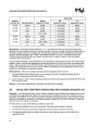
Basic 60- and 66-MHz Pentium@ Processor Identification Information
CPUID
Type Family Model
Stepping
Mfg.
Stepping
Speed
(MHz)
Core/Bus
S-Spec
Vee
Notes
0°C-85°C
1,2
0
5
1
3
50/50
00399
4.75V-5.25V
0
5
1
3
81'
60/60
00352
4.75V-5.25V
0°C-85°C
1
0
5
1
3
81'
60/60
00400
4.75V-5.25V
0°C-75°C
1,2
0
5
1
3
81'
60/60
00394
4.75V-5.25V
0°C-80°C
2,3
0
5
1
3
81'
66/66
00353
4.90V-5.25V
0°C-75°C
1
0
5
1
3
81'
66/66
00395
4.90V-5.25V
0°C-70°C
2,3
0
5
1
3
81"
60/60
00412
4.75V-5.25V
0°C-85°C
1
0
5
1
3
81"
60/60
SX753
4.75V-5.25V
0°C-85°C
1
0
5
1
3
81"
66/66
00413
4.90V-5.40V
0°C-75°C
1
0
5
1
3
81"
66/66
SX754
4.90V-5.40V
0°C-75°C
1,4
0
5
1
5
C1
60/60
00466
4.75V-5.25V
0°C-80°C
3
0
5
1
5
C1
60/60
SX835
4.75V-5.25V
0°C-80°C
3
0
5
1
5
C1
66/66
00467
4.90V-5.40V
0°C-70°C
3
0
5
1
5
C1
66/66
SX837
4.90V-5.40V
0°C-70°C
3
0
5
1
7
01
60/60
00625
4.75V-5.25V
0°C-80°C
3
0
5
1
7
01
60/60
SX948
4.75V-5.25V
0°C-80°C
3
0
5
1
7
01
60/60
SX974
5.15V-5.40V
0°C-70°C
3
0°C-70°C
3
0
5
1
7
01
66/66
00626
4.90V-5.40V
0
5
1
7
01
66/66
SX950
4.90V-5.40V
0°C-70°C
3
0
5
1
7
01
66/66
00627
5.15V-5.40V
0°C-70°C
3
0
5
1
7
01
66/66
SX949
5.15V-5.40V
0°C-70°C
3
NOTES:
1. Non-heat spreader package.
2. These are engineering samples only.
3. Heat spreader package (see Specification Change #2).
4. 66 MHz B1" shipped after work week 34 of 1993 were tested to Vee = 4.90V - 5.40V
4
TeASE
81'
intet
PENTIUM® PROCESSOR SPECIFICATION UPDATE
Summary Table of Changes
The following table indicates the Specification Changes, Errata, Specification Clarifications, or Documentation
Changes which apply to the 60- and 66-MHz Pentium processor. Intel intends to fix some of the errata in a future
stepping of the component, and to account for the other outstanding issues through documentation or
specification changes as noted. This table uses the following notations:
CODES USED IN SUMMARY TABLE
X:
Specification Change or Clarification that applies to this stepping.
Doc:
Document change or update that will be implemented.
Fix:
This erratum is intended to be fixed in a future step of the component.
Fixed:
This erratum has been previously fixed.
(No mark) or (Blank Box):
This erratum is fixed in listed stepping or specification change does not apply to
listed stepping.
NO.
B1
C1
01
Plans
SPECIFICATION CHANGES
1
X
X
X
Doc
Vce Specification Change at 66 MHz
2
X
X
X
Doc
Mechanicalrrhermal/Case Temperature Specifications for Pentium®
Processor Heat Spreader Package
3
X
X
X
Doc
DPO-7 Read Data Setup Time Specification Change
4
X
X
X
Doc
ClK Toggle during Vee Ramp
B1
C1
01
NO.
1
X
2
3
Plans
ERRATA
Fixed
BOFF# hold timing
X
Fixed
Incomplete initialization may flush the intemal pipeline
X
Fixed
IV pin may not be asserted under certain conditions
4
X
Fixed
Testability writes to data TlB may store wrong parity
5
X
Fixed
lRU bits in the data cache TlBs
6
X
Fixed
A replacement writeback cycle may invade a locked sequence
7
X
8
X
X
9
X
X
10
X
X
X
ar~
updated incorrectly
Fixed
RUNBIST instruction generates incorrect BIST signature
Fixed
Data breakpoint mistakenly remembered on a faulty instruction
Doc
RESET affects RUNBIST instruction execution in Boundary Scan
Fixed
locked operation during instruction execution tracing may hang the
processor
5
PENTIUM@ PROCESSOR SPECIFICATION UPDATE
6
intet
intet
PENTIUM@ PROCESSOR SPECIFICATION UPDATE
7
PENTIUM@ PROCESSOR SPECIFICATION UPDATE
SPECIFICATION CHANGES
Specification Changes will be incorporated into the Pentium™ Family User's Manual, Volume 1 and/or Volume 3,
(Order Numbers: 241428 and 241430, respectively).
1.
Vcc Specification Change at 66 MHz
The Vee specification for the Pentium processor operating at 66 MHz is Vee =4.90V to 5.40V. The new Vee
range extends the operating Vee limit at the high end by 150mV over the previous Vee range as shown in the
table below.
Operating Vee Range at 66 MHz
2.
Old
New
4.90V to 5.25V
4.90V to 5.40V
MechanicalffhermallCase Temperature Specifications for Pentium@
Processor Heat Spreader Package
Following are the changes to the Pentium processor mechanical, thermal, and case temperature specifications
necessitated by the addition of a heat spreader to the package for improved thermal performance of the die.
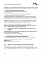
MECHANICAL SPECIFICATIONS
The changes to the Pentium processor, 273-pin PGA package, mechanical specification (Chapter 9 of the
Pentium™ Family User's Manual, Volume 1, Order Number 241428) are summarized as follows:
1.
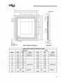
Figure 9-1 is changed to reflect the addition of the heat spreader.
2.
Figure 9-2 added to show the top view of the package.
3.
Table 9-2 updated.
4.
The weight of the heat spreader package increases to approximately 2X the weight of the standard PGA
package (70.7 grams vs. 33.2 grams).
The following two figures show the new package dimensions for the Pentium processor. The mechanical
specifications are provided in the table following these figures.
8
int"et
PENTIUM® PROCESSOR SPECIFICATION UPDATE
I I
SEATING
~~~~=~=~~=~~=~~=~0~,;-~~~-~-_-~-~-~-~s-,~-~~~~~PLAN~~A4
I
0000000000000000000
00
00
00
00
00
00
00
00
00
00
00
00
00
00
00
00
00
00
00
00
0
0
000000000 0000 0
00 0
PIN 04
(signal 01
0
0
0
00
a
o
0
a
0
0
0000
0000
0000
0000
o
0
0
0000
0000
o
0
0
0000
0000
0000
0000
0000
0000
0000
0000
02
0000
0000
0000
0000
00 0
00
t,
E
0
0000
0000
0
0
00000000000000000
000000000000000000000
000000000000000000000
00000
oaooo
00 00 00 0
0
00 0
A
t·29 REF.
~~'i~AcMd'i\'rI\;R)
A'
A2
Sase
Plane
------- D -----~
..
~I..I------D·----~I
..
1011
..
I..
-.......
-...........
D'
r-.
I
tI
r
V CuWHeal SII ea:ler
V
V
Braz eMelal iz al ion
~
D.
Top View of PackaQe
9
intet
PENTIUM@ PROCESSOR SPECIFICATION UPDATE
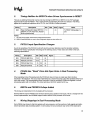
Pentium@ Processor Mechanical Specifications
Family: Ceramic Pin Grid Array Package
Millimeters
Inches
Symbol
Min
Max
Notes
Min
Max
Notes
A
3.91
4.70
Solid Lid
0.154
0.185
Solid Lid
A1
0.38
0.43
Solid Lid
0.015
0.017
Solid Lid
A2
2.62
2.97
0.103
0.117
A4
0.97
1.22
0.038
0.048
B
0.43
0.51
0.017
0.020
0
54.66
55.07
2.152
2.168
01
50.67
50.93
1.995
2.005
02
37.85
38.35
Spreader Size
1.490
1.510
Spreader Size
03
40.335
40.945
Braze
1.588
1.612
Braze
04
E1
8.382
2.29
2.79
F
L
2.54
Flatness of spreader
measured diagonally
0.005
3.30
0.120
273
1.651
0.110
0.090
0.127
N
S1
0.330
Total Pins
Flatness of spreader
measured diagonally
0.130
Total Pins
273
2.16
0.065
0.085
THERMAL SPECIFICATIONS
The following table provides the new thermal parameter specifications for the Pentium processor heat spreader
package:
Junction-to-Case and Case-to-Ambient Thermal Resistances for the Pentium@ Processor
(With and Without a Heat Sink')
9 CA2 vs. Airflow (ftlmin)
9 JC
0
200
400
600
800
1000
With 0.25" Heat Sink
0.6
8.3
5.4
3.5
2.6
2.1
1.8
With 0.35" Heat Sink
0.6
7.4
4.5
3.0
2.2
1.8
1.6
With 0.65" Heat Sink
0.6
5.9
3.0
1.9
1.5
1.2
1.1
Without Heat Sink
1.2
10.5
7.9
5.5
3.8
2.8
2.4
NOTES:
1.
Heat Sink: 2.1 sq. in. base, omni-directional pin AI heat sink with 0.050 in. pin width, 0.143 in pin-to-pin center spacing and
0.150 in. base thickness. Heat sinks are attached to the package with a 2 to 4 mil thick layer of typical thermal grease. The
thermal conductivity of this grease is about 1.2 w/m DC.
2.
eCA values are typical values. The actual eCA values depend on the air flow in the system (which is typically unsteady,
non-uniform and turbulent) and thermal interactions between Pentium processor and surrounding components through
PCB and the ambient.
10
PENTIUM® PROCESSOR SPECIFICATION UPDATE
The following is a description of how the heat spreader improves the package thermal performance:
Since the Pentium processor requires an external heat sink in order to maintain the junction and case
temperatures below the acceptable levels, the main contributors to the total junction to ambient thermal
resistance are junction to case (8J cl, case to heat sink (8cs ), and heat sink to ambient (8s A) thermal
resistances.
8 JC is mainly a function of internal construction of the package and packaging material, thermal properties such
as the die size and die attach, and ceramic thermal conductivity. 8 cs is a function of the thickness and thermal
properties of the interface material between the package and heat sink, package and heat sink flatness, and
surface finish and effective heat transfer area between the package and the heat sink. 8 SA is a function of both
the heat sink design and the airflow type and rate.
Using a heat spreader in the package lowers the overall thermal resistance in two ways:
1.
It increases the effective heat transfer area between the package and the heat sink and as a result lowers
8 cs . The actual reduction in 8 cs depends on the magnitude of 8 cs without a heat spreader. The larger
the value of 8 cs without using a heat spreader, the larger will be the reduction in the value of 8 JA if a heat
spreader is used.
2.
A heat spreader may also improve the heat sink thermal performance by increasing the effective heat
transfer area in the heat sink and making the fins away from the die more effective.
Using a heat spreader with a thermal grease interface will result in about .4 c/w lower 8 CA than that for the
package without the heat spreader. Thermal grease is considered one of the more thermally efficient materials
for use as an interface between heat sink and package. Thermally conductive adhesives and conductive tapes
or films typically have poorer thermal performance when compared to a thin layer of thermal grease, because
grease facilitates a larger reduction in thermal resistance.
CASE TEMPERATURE SPECIFICATIONS
Following are the case temperature specifications for the Pentium processor with and without the heat spreader
on the package:
Pentium@ Processor Package Without Heat Spreader
The case temperature specifications for the Pentium processor package without heat spreader at 60 and 66
MHz are as follows (Note: This applies to Bl" and previous steppings):
1.
T C (case temperature) O°C to 85°C @60 MHz.
2.
TC (case temperature) O°C to 75°C @66 MHz.
Pentium@ Processor With Heat Spreader Package
The case temperature specifications for the Pentium processor heat spreader package at 60 and 66 MHz are as
follows (Note: This applies to Cl and later steppings):
1.
Tc (case temperature) O°C to 80°C @60 MHz.
2.
Tc (case temperature) O°C to 70°C @66 MHz.
In the case of the Pentium processor with heat spreader package, the case temperature is measured at the
center of the package top surface on the heat spreader. The procedure to measure the case temperature, is
outlined in Chapter 10 of the Pentium™ Family User's Manual, Volume 1 (Order Number 241428).
The thermal specification of the heat spreader package calls for 5 degrees Celsius lower case temperature than
the non-spreader package for both 60- and 66-MHz versions. The lower case temperature requirement of the
heat spreader package is due to its lower junction to ambient thermal resistance compared to a non-heat
11
PENTIUM@ PROCESSOR SPECIFICATION UPDATE
intet
spreader package with the same heat sink. For example, at 66-MHz, the heat spreader package will have
0.4*16=6.4 degrees Celsius lower case temperature than a non-heat spreader package with the same heat sink
design and grease interface. This implies that in a system designed for a non-spreader package, if the nonspreader package is replaced with a heat spreader package, the measured case temperature will be lower by
6.4 degrees Celsius for the 66-MHz and 5.8 degrees Celsius for the 60-MHz versions. The actual reduction in
the case temperature will be slightly higher or lower depending on the efficiency of the thermal interface.
Therefore, a more conservative value of 5 degrees Celsius is used as the difference between the case
temperature specifications of the two package types for both frequency versions. The expectation is that the
ambient temperature in the system will be maintained while gaining the benefits of lower junction and case
temperatures when the heat spreader package is added to an existing system with the same airflow and
unmodified heat sink.
3.
DP[7:0] Read Data Setup Time Specification Change
The following tables show the new A.C. Specification for the Data Parity (DPO-7) Read Data Setup Time for the
Pentium processor at 66 and 60 MHz:
Parameter
DPO-7 Read Data Setup Time
Parameter
DPO-7 Read Data Setup Time
4.
CLK Toggle during Vee Ramp
The following note has been added to the clock pin description: 'It is recommended that ClK begin toggling
within 150 ms after Vee reaches its proper operating level. This recommendation is only to ensure long-term
reliability of the device.'
12
intet
PENTIUM@ PROCESSOR SPECIFICATION UPDATE
ERRATA
1.
BOFF# Hold Timing
PROBLEM: Silicon characterization indicates that the processor does not meet the specified hold time, 1.5ns,
for the BOFF# signal. Data indicates that a minimum hold time of 2.0ns is required.
IMPLICATION: If a minimum hold time of 2.0ns is not met for the BOFF# input, the processor may drive
undefined or incorrect cycles on to the external bus.
WORKAROUNO: System must guarantee a minimum hold time of 2.0ns at the BOFF# input to the Pentium
processor.
STATUS: This erratum is fixed to meet the minimum specified hold time of 1.5ns on the C-stepping.
2.
Incomplete Initialization May Flush the Internal Pipeline
PROBLEM: If a memory write occurs before the first branch instruction immediately after RESET, then the
internal pipeline may get flushed unexpectedly. Assuming normal distribution of code space, this unexpected
flush has the probability of 1 in 226 of occurring.
IMPLICATION: The probability of this unexpected flush occurring is very low. When it happens, its only effect is
to flush the internal pipeline and re-fetch the correct opcodes again. The instructions will still be executed
correctly.
In the FRC (Functional Redundancy Checking) environment, where the clock-by-clock behavior of the processor
needs to be checked deterministically, it may cause the system to report an error.
WORKAROUNO: After RESET, ensure that the first write to memory occurs after a branch instruction.
STATUS: This erratum is fixed on the C-stepping.
3.
IVPin May Not Be Asserted under Certain Conditions
PROBLEM: The IV pin is driven active by the Pentium processor to indicate that an instruction in the v-pipe has
completed execution. In the following case, the IV pin may not get asserted:
When a mispredicted instruction (pair) reaches the execution stage, it will cause a pipeline flush. If in this clock,
a fault is detected on the instruction in the u-pipe, the IV pin will not be asserted for a v-pipe instruction of the
next instruction pair which is executed next.
IMPLICATION: The lact that the IV pin is not asserted under certain conditions will affect the reliability of the
execution tracing data. It will also affect the performance monitoring event count for instructions executed in the
v-pipe.
WORKAROUNO: Disabling the v-pipe will allow execution tracing to work properly.
STATUS: This erratum is fixed on the C-stepping.
13
PENTIUM@ PROCESSOR SPECIFICATION UPDATE
4.
intet
Testability Writes to Data TLB May Store Wrong Parity
PROBLEM: During testability writes to the data TLB, an incorrect tag parity may be computed and stored with
the tag address. Subsequently, when this entry is read during a normal (non-testability) cycle, an internal parity
error (lERR#) may be generated.
IMPLICATION: The internal parity error may occur only if a non-testability access is made to the same data TLB
entry which had been previously written on a testability write. This problem will not show up if the data TLB is
flushed after having been used for testability purposes using the TLB test registers.
WORKAROUNO: Ensure that the data TLB is flushed after having been used for testability writes and before
being used for normal operation.
STATUS: This erratum is fixed on the C-stepping.
5.
LRU Bits in the Data Cache TLBs Are Updated Incorrectly
PROBLEM: Due to a circuit problem, the LRU bits for the data cache TLBs are updated incorrectly when both
the u and v pipes access the same set. As the TLBs are organized as 4-Way set associative, more specifically
this problem occurs when a u-pipe match is found on Way 0 and a v-pipe match is found on Way 1, or the u-pipe
match is found on Way 2 and the v-pipe match is found on Way 3 of the same set.
IMPLICATION: The LRU bits are used to handle replacements in the TLB. In this specific case, the pseudo LRU
mechanism is not strictly adhered to. Any performance degradation resulting from this is expected to be
negligible.
WORKAROUNO: None
STATUS: This erratum is fixed on the C-stepping.
6.
A Replacement Writeback Cycle May Invade a Locked Sequence
PROBLEM: During a locked read-modify-write (RMW) sequence, if BOFF# or AHOLD is asserted before the
write portion of the RMW sequence is completed, then the write cycle will be held off in the internal write buffer
until the BOFF# or AHOLD Signal is deasserted. During the time that the bus is backed off, if another locked
instruction (Le., with a LOCK prefix) enters the instruction pipeline and initiates a replacement writeback in the
data cache, then as soon as the bus is freed, the write back cycle due to the replacement write back may be
issued in front of the locked write cycle pending in the write buffer. After completion of the write back cycle, the
processor will issue the write cycle to complete the RMW sequence.
IMPLICATION: This problem will only affect those systems which do not expect a replacement writeback cycle in
the middle of a locked RMW sequence. Furthermore, the timing of events needed for the above problem to
manifest itself has a low probability of occurrence. Note that even though the bus cycles are reordered in this
case, the correct bus cycles are run and should not cause any data coherency problems.
WORKAROUNO: Do not assert BOFF# or AHOLD in between the read and the write portion of a locked readmodify-write sequence.
STATUS: This erratum is fixed on the C-stepping.
14
int"et
7.
PENTIUM® PROCESSOR SPECIFICATION UPDATE
RUNBIST Instruction Generates Incorrect BIST Signature
PROBLEM: The Pentium processor TAP instruction, RUNBIST, generates incorrect BIST signature if issued
while the processor is in Probe mode. The BIST result is also incorrect if the RUNBIST instruction is issued
during a repeated MOVS (move data from string to string) instruction.
IMPLICATION: The BIST may report an incorrect signature indicating self-test failure even though the processor
may not be faulty.
WORKAROUNO: Do not issue the (TAP) RUNBIST instruction when the processor is in Probe mode, or during a
repeated MOVS instruction.
STATUS: This erratum is fixed on the C-stepping.
8.
Data Breakpoint Mistakenly Remembered on a Faulty Instruction
PROBLEM: In the following two cases, an instruction that has data breakpoints enabled and also generates a
fault before completing execution may cause an unexpected data breakpoint to occur later in the code or may
cause the software to hang:
CASE 1:
For the first failing case to occur, the data breakpoint must be set on an instruction that is not a simple
instruction (Note: simple instructions are those that are entirely hardwired and do not require any microcode
control) and includes multiple memory references (e.g., a read operation followed by a write operation). In
addition, this instruction also generates a fault before completing execution. The data breakpoint must be set on
one memory operation (e.g., a data read portion), and the fault occurs on a subsequent memory operation (e.g.,
a data write portion). If later in the code, a fault during a repeated string operation is encountered, then a
spurious debug exception will be reported first, followed by the fault for the string operation. This unexpected
debug exception during the string operation may only occur if no other debug exception is taken before the string
operation Is executed.
CASE 2:
For the second failing case, the data breakpoint must be set on the data read of iteration X of a repeated string
instruction, and a fault must occur on the data write of the same iteration X. In this case, the Pentium processor
takes the debug exception first, before handling the fault. When the faulting iteration is restarted after the debug
exception is handled, the data breakpoint is again detected when the fault is encountered, and the processor
returns to the debug exception handler. This will cause repeated entries into the debug exception handler for the
same iteration. This loop may occur forever, unless the debug exception handler modifies the data breakpoints
or the return instruction pOinter.
IMPLICATION: In the first case, a data breakpoint may occur when it is not expected. In the second case, a
repeated string instruction has a data breakpoint set on the read portion and a fault occurs on the corresponding
write. This may cause the software to hang.
WORKAROUNO: When setting data breakpoints, be aware of the above failure cases. Note that code and lID
breakpoints can be set properly and are not affected by this erratum.
STATUS: This erratum is fixed in the D-stepping.
15
PENTIUM@ PROCESSOR SPECIFICATION UPDATE
9.
intet
RESET Affects RUNBIST Instruction Execution in Boundary Scan
PROBLEM: The Boundary Scan TAP instruction, RUNBIST, is affected by the assertion of the RESET pin. If the
RESET pin is asserted while the processor is executing the TAP instruction, RUNBIST (TAP command field =
0111, and the TAP controller is in the Run-Test-Idle state), then the processor indicates a BIST failure.
IMPLICATION: The IEEE 1149.1-1990 specification states "the design of the component shall ensure that
results of the self-tests executed in response to the RUNBIST instruction are not affected by signals received at
the non-clock system input pins". The Pentium processor does not meet this requirement.
WORKAROUNO: Ensure that the RESET pin is deasserted while the RUNBIST (TAP) instruction is executing.
STATUS: This erratum affects all steppings of the 60- and 66-MHz Pentium processor.
10.
Locked Operation during Instruction Execution Tracing May Hang
the Processor
PROBLEM: During instruction execution tracing (TR12.TR bit set to '1 ') the processor can internally buffer up to
two Branch Trace messages. If there is a possibility of a third Branch Trace message being delivered from the
instruction being executed, the machine will stall in order to avoid overwriting either of the two messages that are
already buffered. If this instruction is performing a "locked read-modify-write" operation, the processor can hang
up due to internal service contention for the bus controller logic.
IMPLICATION: This problem does not affect normal operation (TR12.TR bit is not set). It only affects operation
while the instruction execution tracing feature is enabled. A hardware RESET will be required to get the
processor out of the deadlock condition if it occurs.
WORKAROUNO: Do not enable instruction execution tracing.
STATUS: This erratum is fixed in the D-stepping.
11.
Breakpoint or Single-Step May Be Missed for One Instruction
Following STI
PROBLEM: If the next instruction following STI is the target of a mispredicted branch, the processor may shut
off the interrupt window for one instruction following STI. This will prevent breakpoints, single-step or other
external interrupts from being recognized during this time.
IMPLICATION: The processor may not recognize NMI, SMI#, INIT, FLUSH#, BUSCHK#, R/S#, code/data
breakpoint and single-step for one instruction after executing STI. This is not a problem unless breakpoints or
single stepping is used. The only possible effect is that they may be missed.
WORKAROUNO: Do not set a breakpoint on the next sequential instruction after STI. Alternatively, disabling
branch prediction will prevent this problem from occurring.
STATUS: This erratum is fixed in the D-stepping.
12.
Internal Snoop Problem Due to Reflection on Address Bus
PROBLEM: An internal snoop occurs in the following three cases:
1.
An access is made to the code cache, and that access is a miss.
2.
An access is made to the data cache, and that access is a miss or a write-through.
16
intet
3.
PENTIUM® PROCESSOR SPECIFICATION UPDATE
There is an access to the page tableldirectory entries.
In all of these cases, the address used for the internal snoop is obtained from the input buffer of the address 1/0
buffers inside the chip. If there is signal reflection on the address lines A[31 :5] which causes the setup/hold time
inside the chip to be violated, then the internal snoop may fail.
When the reflection on the address 1/0 buffer is above (or below) the trip point of an input buffer (Le., 1.5V for a
TTL input) for a high to low (or low to high) transition, then the internal snoop address will not be valid until after
the address reflection falls below (or transitions above) the trip point in the clock ADS# and address is driven. If
the reflection causes the wrong snoop address A[31 :5] to be latched inside the chip due to setuplhold time
violation, then an incorrect internal snoop may occur.
IMPLICATION: When the failure occurs, a wrong cache line may be snooped causing either a line to remain valid
when it should not, a valid line to become invalid when it should not, or an invalid line to be snooped.
In the first case, when a valid line should be invalidated and is not, a cache coherency problem between the
code and data cache is possible (e.g., self-modifying code). In the second case, when a valid cache line is
incorrectly made invalid, an unexpected writeback cycle may occur if the line was in the modified state, and an
unexpected bus cycle may occur to re-allocate the cache line. The third case, where an invalid line is snooped,
will not cause any detectable failure.
An additional failure mechanism can be seen if address lines A[11 :5] are transitioning while being sampled. In
this case, the internal snoop may fail, causing a tag parity error during the snoop resulting in an IERR#
assertion.
The magnitude of the reflection is dependent upon the 1/0 buffer vs. transmission line impedance mismatch and
the lengthllayout of trace (transmission line). There is sufficient margin built into the external timing specification
for the address bus and 1/0 buffer models, and it is not expected that any failures will be seen on existing
systems. In a lab enVironment, a failure was forced by adding a 12 inch coaxial cable (with no termination) along
with a 330 ohm pull-up resistor on the address line to induce excessive reflection. Removing either the pull-up
resistor or adding termination to the coaxial cable eliminated the failure.
WORKAROUNO: To avoid any internal snoop failures, ensure that the address A[31 :5] setup and hold times are
not violated at the processor's input due to reflection in the clock in which the processor drives the address bus
and ADS# is asserted. Note: Meeting the setup and hold times at the processor's input is not necessary in the
clocks where ADS# is not asserted.
STATUS: This erratum is fixed in the D-stepping.
13.
Internal Parity Error on Uninitialized Data Cache Entry
PROBLEM: In the following case, an incorrect internal parity error (IERR#) may be reported due to an
uninitialized entry in the data cache during a special qword (64-bit) read. This may occur if the qword read
issued to the u-pipe is also followed by a v-pipe read, and the v-pipe read is to a different odd bank and different
way than the u-pipe qword read. In addition, the u-pipe address corresponding to this different way must have
invalid and uninitialized data. Under these conditions, the processor may check the invalid data for parity errors
and incorrectly assert the IERR# pin.
IMPLICATION: After power-on reset, before the data cache is completely initialized, the processor may
incorrectly report an IERR# and shutdown.
WORKAROUNO: After power-on reset, initialize all entries in the data cache before the cache is enabled. The
easiest way to do this is to invoke BIST (built-in self test) after reset. Alternatively, software can initialize the data
cache by reading data from memory appropriately, or writing into all its locations through the cache test
registers.
STATUS: This erratum is fixed in the D-stepping.
17
PENTIUM® PROCESSOR SPECIFICATION UPDATE
14.
Missing Shutdown after an IERR#
PROBLEM: If an internal parity error is reported to the IERR# pin and a mispredicted branch or a
trap/faultlinterrupt with a higher priority than shutdown occurs, then the processor may not shutdown.
IMPLICATIONS: During the reporting of an internal parity error, the IERR# pin may go active without a processor
shutdown. Note that IERR# due to an internal parity error will not occur unless the parity error is induced through
parity reversal testing or if the chip is defective.
WORKAROUND: The system can latch an IERR# assertion at the processor clock edge and force a shutdown
by asserting NMI or initializing the processor through RESET or INIT. Note: IERR# is a glitch free signal, so no
spurious assertions of IERR# will occur.
STATUS: This erratum is fixed in the D-stepping.
15.
Processor Core May Not Serialize on Bus Idle
PROBLEM: Under rare circumstances, the processor may not serialize with the bus when the processor core is
waiting for the bus to finish pending cycles and BOFF# is asserted. The processor will not reorder bus cycles; it
may only start with the next event (fetching and executing subsequent instructions) before waiting for all pending
bus cycles to complete. The following cases have been identified that may be affected by this:
SMI# pending
If BOFF# is used to back off a bus cycle while an SMI# is pending, the
processor may assert SMIACT# before re-starting the aborted bus cycles.
Serializing instruction
If BOFF# is used to back off a bus cycle due to a serializing instruction, the
processor may start executing the next instruction before restarting or
completing the previous bus cycle. The processor, however, will not reorder
any bus cycles for the new instruction in front of bus cycles for the previous
instruction.
Invalidation during cache line fill
If BOFF# is used to back off a cache line fill and BOFF# occurs after the data
has been returned to the processor but before the end of the line fill, an
invalidation request during this time may result in the cache invalidation to
occur before the line fill has completed, This may cause the cache line to
remain in a valid state after the invalidation has completed. Note that if the
invalidation request comes in via WBINVD or FLUSH#, the line fill would have
to be backed off at least twice (or once for INVD) in order for the cache line to
remain in a valid state after the invalidation has completed.
OUT instruction
If BOFF# is used to back off a bus cycle due to an OUT instruction, the
processor may start executing the next instruction before the bus cycle due to
OUT has completed (note: the OUT instruction is similar to the serializing
instructions except that it does not stop the prefetch of the subsequent
instruction). The processor, however, will not reorder any bus cycles for the
new instruction in front of the OUT bus cycle.
IMPLICATION: This problem has only been observed in internal test vehicles. The events described above have
different possible implications as follows:
SMI# pending
The processor may enter SMM before restarting the aborted bus cycle. The
SMIACT# assertion may cause the restarted bus cycle to run to SMRAM
space.
Serializing Instruction
Since the cycles are not reordered, a system should not encounter any
problems unless it depends on the serializing instruction to cause an external
event prior to execution of the next instruction.
18
intet
PENTIUM® PROCESSOR SPECIFICATION UPDATE
Invalidation during cache line fill
In a rare instance, a cache line may remain in the valid state (E or S state)
after the cache invalidation has completed.
OUT instruction
Since the cycles are not reordered, a system should not encounter any
problems unless it depends on the OUT instruction to cause an external
event prior to execution of the next instruction. For example, an OUT
instruction may be used to assert the A20M# signal prior to the next
instruction. In this case, observed code has followed the OUT with an I/O
read (IN) to ensure the signal is properly asserted. A second case, could be
using an OUT instruction to configure/initialize and interrupt controller and
follow it with STI to enable interrupts. Once again no failure would be
observed. The controller would respond with the spurious interrupt vector.
WORKAROUND: Restrict the use of BOFF# for the described events. In addition, the SMI# pending event can
be eliminated by locating SMRAM so that it does not shadow standard memory and does not require SMIACT#
for memory decode. The OUT or serializing instruction events are eliminated if the next instruction does not
depend on the result of the event before executing the instruction.
STATUS: This erratum is fixed in the D-stepping.
16.
SMIACT# Assertion during Replacement Writeback Cycle
PROBLEM: If a data read cycle triggers a replacement write back cycle and the SMI# signal is asserted prior to
the first BRDY# of the read cycle, the processor may assert the SMIACT# signal prematurely.
Before the processor asserts SMIACT# in response to an SMI# request, it should complete all pending write
cycles (including emptying the write buffers). However, if the appropriate conditions occur, the SMIACT# signal
may get asserted during the replacement writeback cycle a few clocks after the last BRDY# of the read cycle.
IMPLICATION: If the SMIACT# signal is used by the system logic to decode SMRAM (e.g., SMRAM is located in
an area that is overlaid on top of normal cacheable memory space), then the replacement writeback cycle with
SMIACT# asserted could occur to SMM space. Systems that locate SMRAM in its own distinct memory space
(non-overlaid) should not be affected by this.
WORKAROUND: Asserting FLUSH# simultaneously with SMI# will prevent this problem from occurring. In
systems that overlay SMRAM over normal cacheable memory space, this is already a necessary requirement to
maintain cache coherency.
STATUS: This erratum is fixed in the D-stepping.
17.
Overflow Undetected on Some Numbers on FIST
PROBLEM: On certain large positive input floating point numbers, and only in two processor rounding modes,
the instructions FIST[P] m16int and FIST[P] m32int fail to process integer overflow. As a consequence, the
expected exception response for this situation is not correctly provided. Instead, a zero is returned to memory as
the result.
The problem occurs only when all of the following conditions are met:
1.
The FIST[P] instruction is either a 16- or 32-bit operation; 64-bit operations are unaffected.
2.
Either the 'nearest' or 'up' rounding modes are being used. Both 'chop' and 'down' rounding modes are
unaffected by this erratum.
3.
The sign bit of the floating point operand is positive.
19
intet
PENTIUM® PROCESSOR SPECIFICATION UPDATE
4.
The operand is one of a very limited number of operands. The table below lists the operands that are
affected. For an operand to be affected, it must have an exponent equal to the value listed and a significand
with the most significant bits equal to '1'. Additionally, in the 'up' rounding mode, at least one of the remaining
lower bits of the significand must be '1'. The Exponent and the two Significand columns describe the
affected operands exactly, while the values in the column titled 'Approximate Affected Range' are only for
clarity.
FIST[P]
Operation
Rounding
Mode
Unbiased
Exponent
Upper Bits of
Significand
Lower Bits of
Significand
Approximate Affected Range
16-bit
Up
15
='1'
17 MSS's ='1'
32 MSS's ='1'
33 MSS's ='1'
At least one '1'
65,535.50 ±0.50
Nearest
15
Up
31
Nearest
31
32-bit
64-bit
16 MSS's
Don't care
65,535.75 ± 0.25
At least one '1'
4,294,967,295.50 ± 0.50
Don't care
4,294,967,295.75 ± 0.25
Problem does not occur
ACTUAL vs. EXPECTED RESPONSE
Actual Response
When the flaw is encountered, the processor provides the following response:
•
A zero is returned as a result. This result gets stored to memory.
•
The IE (Invalid Operation) bit in the FPU status word is not set to flag the overflow.
The C1 (roundup) and PE bits in the FPU status word may be incorrectly updated.
•
No event handler is ever invoked.
Expected Response
The expected processor response when the invalid operation exception is masked is:
•
Return a value 10000 .... 0000 to memory.
•
Set the IE bit in the FPU status word.
The expected processor response when the invalid operation exception is unmasked is:
•
Do not return a result to memory. Keep the original operand intact on the stack.
•
Set the IE bit in the FPU status word.
•
Appropriately vector to the user numeric exception handler.
IMPLICATIONS: An unexpected result will be returned when an overflow condition occurs without being
processed or flagged. Integer overflow occurs rarely in applications. When overflow does occur, the likelihood of
the operand being in the range of affected numbers is even more rare. The range of numbers affected by this
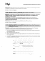
erratum is outside that which can be converted to an integer value. The figure below and corresponding table
detail the normal range of numbers (between A and S) and the range affected by this erratum (between C
and D).
20
intet
PENTIUM® PROCESSOR SPECIFICATION UPDATE
A
OVerflow
o
C D
B
Normal Range
OVerflow
\
Affected
Range
16-bit Operation
A
B
C
D
Round Nearest
(-32,768.5)
(+32,767.5)
[+65,535.5]
(+65,536.0)
Round Up
(-32,769.0)
[+32,767.0]
(+65,535.0)
(+65,536.0)
32-bit Operation
A
B
C
D
Round Nearest
[-2,147,483,648.5]
(+2,147,483,647.5)
[+4,294,967,295.5]
(+4,294,967,296.0)
Round Up
(-2,147,483,649.0)
[+2,147,483,647.0]
(+4,294,967,295.0)
(+4,294,967,296.0)
NOTE:
[xxx.x] indicates the endpoint is included in the interval; (xxx.x) indicates the endpoint is not included in the interval.
Furthermore, given that the problem cannot occur in the 'chop' rounding mode, and given that the 'chop'
rounding mode is the standard rounding mode in ANSI-C and ANSI-FORTRAN 77, it is unlikely that this
condition will occur in most applications.
This erratum is not believed to affect application programs in general. Applications will need to handle
exceptional behavior and take the appropriate actions to recover from exceptions. In order to do this applications
will need to do either range checking prior to conversion or implement explicit exception handling. If an
application relies on explicit exception handling the possibility of an error exists. It is, however, believed that
applications written in languages that support exception handling will most likely do range checking, thereby
allowing the application to be compiled with a no check option for performance reasons when the application has
been debugged.
WORKAROUND: Any of three software workarounds will completely avoid occurrence of this erratum:
1.
Range checking performed prior to execution of the FIST[P] instruction will avoid the overflow condition from
occurring. This is common program practice.
2.
Use the 'chop' or 'down' rounding modes. This erratum will never occur in these modes. By default, both
ANSI-C and FORTRAN will use the 'chop' mode.
3.
Use the FRNDINT (Round floating-point value to integer) instruction immediately preceding FIST[P].
FRNDINT will always round the value correctly.
STATUS: This erratum is present in all steppings of the 60- and 66-MHz Pentium processor.
18_
Six Operands Result in Unexpected FIST Operation
PROBLEM: For six possible operands and only in two processor rounding modes (up, down), the FIST or FISTP
(floating-point to integer conversion and store) instructions return unexpected results to memory. Additionally,
incorrect status information is returned under certain conditions in all 4 rounding modes.
The flaw occurs only on certain operands on the instructions FIST[P] m16int, FIST[P] m32int, and FIST[P]
m64int. These operands are ± 0.0625, ± 0.125, and ± 0.1875.
The following table details the conditions for the flaw and the results returned. For use of any of the six abovelisted operands, refer to the left-hand side of the table in the column for a given combination of sign and rounding
mode. The corresponding right-hand side of the table shows the results which will occur for the given conditions.
21
intet
PENTIUM@pROCESSOR SPECIFICATION UPDATE
These results include the C1 (Condition Code 1) and PE (Precision Exception) bits and, in two instances, storing
of unexpected results.
Status Bits
Operand
(anyone of)
Rounding
Mode
Result
Expected I Actual
PE
Expected I Actual
+0.0625
nearest
SAME
1 I Unchanged
SAME
+0.1250
chop
SAME
1 / Unchanged
SAME
+0.1875
down
SAME
1 / Unchanged
SAME
up
0001/0000
1 / Unchanged
1/0
nearest
SAME
1 / Unchanged
SAME
SAME
-0.0625
C1
Expected I Actual
-0.1250
chop
SAME
1 / Unchanged
-0.1875
down
- 0001 /0000
1 / Unchanged
1 /0
up
SAME
1 / Unchanged
SAME
IMPLICATIONS: An incorrect result (0 instead of + 1 or -1) is returned to memory for the six previously listed
operands. Incorrect results are returned to memory only when in the 'up' rounding mode with a positive sign or in
the 'down' rounding mode with a negative sign. The majority of applications will be unaffected by this erratum
since the standard rounding mode in ANSI-C and ANSI-FORTRAN 77 is 'chop', while BASIC and the ISO
PASCAL intrinsic ROUND function use 'nearest' rounding mode. In addition, 'nearest' is also the default
rounding mode in the processor.
Incorrect status information is also insignificant to most applications. Given that the PE bit in the numeric status
register is 'sticky', and that most floating point instructions will set this bit, PE will most likely have already been
set to '1' before execution of the FIST[Pj instruction and therefore, the PE bit will not be seen to be incorrect. In
addition, the unexpected values for the C1 bit are unlikely to be significant for most applications since the only
usage of this information is in exception handling.
WORKAROUND: Either of two software workarounds will completely avoid this erratum:
1.
Use the FRNDINT (round floating-point value to integer) instruction immediately preceding FIST[Pj.
FRNDINT will always round the value correctly.
2.
Use of 'nearest' or 'chop' modes will always avoid any incorrect result being stored (although the PE bit may
have incorrect values).
STATUS: This erratum is present in all steppings of the 60- and 66-MHz Pentium processor.
19.
Snoop with Table-Walk Violation May Not Invalidate Snooped Line
PROBLEM: If an internal snoop (as a result of ADS#) or external snoop (EADS#) with invalidation (INV) occurs
coincident with a page table walk violation, the snoop may fail to invalidate the entry in the instruction cache. A
page table walk violation occurs when the processor speculatively prefetches across a page boundary and this
page is not accessible or not present. This violation results in a page fault if this code is executed. A page fault
does not occur if the code is not executed.
For this erratum to occur, all the following conditions must be met:
1.
A snoop with invalidation is run in the code cache. The snoop may be internal or external.
2.
The Pentium processor is performing a page table walk to service an instruction TLB miss.
22
PENTIUM@ PROCESSOR SPECIFICATION UPDATE
3.
The page table walk results in a violation (this mayor may not lead to a page or other fault due to a
speculative fetch).
4.
The EADS# of the external snoop or ADS# of the table update occur within the window of failure.
The window is defined by:
a.
2-4 clocks after BRDY# is retumed for the page directory or table read.
b.
2-n clocks after BRDY# is returned for the page directory or table read if the set address of a buffered
write matches that of the instruction cache lookup. "n" is determined by the time to complete two new
data write bus cycles from the data cache.
IMPLICATION: This erratum has not been observed on any system. It was found only through investigation of
component schematics, and Intel has only duplicated it on a proprietary test system by forcing failure conditions
using the internal test registers. The low frequency of occurrence is due to the way most systems operate; DMA
devices snoop code 4 bytes at a time so that each line would get snooped and invalidated multiple times.
If this erratum occurs and a line is not invalidated in the instruction cache, then the instruction cache may have a
coherency problem. As a result the processor may execute incorrect instructions leading to a GPF or an
application error. This erratum affects only self-modifying code and bus masterslDMA devices. Due to
necessary conditions, this erratum is expected to have an extremely low frequency of occurrence.
WORKAROUNO: There are two workarounds. Because of the rarity of occurrence of this erratum, Intel does not
believe that there is need to implement a workaround.
1.
Rewrite the device driver for the DMA devices such that after DMA is complete, the instruction cache is
invalidated using the TRS.cntl=11 (flush) and CD=O (code cache) bits.
2.
Disable the L 1 cache.
STATUS: Fixed on the D stepping of 60- and 66-MHz Pentium processor.
20.
Slight Precision Loss for Floating Point Divides on Specific Operand
Pairs
PROBLEM: For certain input datum the divide, remaindering, tangent and arctangent Floating Point instructions
produce results with reduced precision.
The odds of encountering the erratum are highly dependent upon the input data. Statistical characterization
yields a probability that about one in nine billion randomly fed operand pairs on the divide instruction will produce
results with reduced preCision. The statistical fraction of the total input number space prone to failure is
1.14x10·'O • The degree of inaccuracy of the result delivered depends upon the input data and upon the instruction
involved. On the divide, tangent, and arctangent instructions, the worst-case inaccuracy occurs in the 13th
significant binary digit (4th decimal digit). On the remainder instruction, the entire result could be imprecise.
This flaw can occur in all three precision modes (single, double, extended), and is independent of rounding
mode. This flaw requires the binary divisor to have any of the following bit pattems (1.0001, 1.0100, 1.0111,
1.1010 or 1.1101) as the most significant bits, followed by at least six binary ones. This condition is necessary
but not sufficient for the flaw to occur. The instructions that are affected by this erratum are: FDIV, FDIVP,
FDIVR, FDIVRP, FIDIV, FIDIVR, FPREM, FPREM1, FPTAN, FPATAN.
During execution, these instructions use a hardware divider that employs the SRT (Sweeney-Robertson-Tocher)
algorithm which relies upon a quotient prediction PLA. Five PLA entries were omitted. As a result of the
omission, a divisor/remainder pair that hits one of these missing entries during the lookup phase of the SRT
division algorithm will incorrectly predict a intermediate quotient digit value. Subsequently, the iterative algorithm
will return a quotient result with reduced precision.
23
PENTIUM@ PROCESSOR SPECIFICATION UPDATE
intet
The flaw will not occur when a floating point divide is used to calculate the reciprocal of the input operand in
single precision mode, nor will it occur on integer operand pairs that have a value of less than 100,000.
IMPLICATION: For certain input datum, there will be a loss in precision of the result that is produced. The loss in
precision can occur between the 13th and 64th significant binary digit in extended precision. On the remainder
instruction the entire result could be imprecise.
The occurrence of the anomaly depends upon all of the following:
1.
The rate of use of the specific FP Instructions in the Pentium processor.
2.
The data fed to them.
3.
The way in which the results are propagated for further computation by the application.
4.
The way in which the final result of the application is interpreted.
Because of the low probability of the occurrence with respect to the input data (one in nine billion random
operand pairs), this anomaly is of low significance to users unless they exercise the CPU with a very large
number of divides and/or remainder instructions per day, or unless the data fed to the divisor is abnormally high
in sensitive bit patterns.
WORKAROUNO: Due to the extreme rarity of this flaw, a workaround is not necessary for almost all users.
However, Intel is replacing components for end users and OEM's upon request. In addition, a software patch is
available for compiler developers. If you are a compiler developer, contact your local Intel representative to
obtain this, or download from the World Wide Web Intel support server (www.intel.com).
STATUS: Fixed in the D stepping of the 60- and 66-MHz Pentium processor.
A white paper, Statistical Analysis of Floating Point Flaw in the Pentium™ Processor (1994), Order Number
242481, is available that includes a complete analysis performed by Intel.
21.
Power-Up BIST Failure
PROBLEM: The BIST (Built In Self Test) feature may fail.
IMPLICATION: Upon completion of BIST, a false failure may be reported. That is, a non-zero value may be
returned in the EAX register, even though the part is operating correctly. As such, this erratum has no other
product or system implications and is fully functional. To date, all observed false failures have returned a value
of 20000H in EAX.
WORKAROUNO: The root cause of the failure is not yet fully understood. As a result, workarounds suggested in
this document are not 100 percent guaranteed. However, no BIST failures have been observed with use of
either of the workarounds.
There are two workarounds:
1.
24
Invoke a double RESET - All false BIST failures have occurred during cold RESET. In order to accurately
execute BIST, a double RESET sequence may be performed as shown in the figure below:
PENTIUM® PROCESSOR SPECIFICATION UPDATE
First BIST (optional)
-- assumed not run here
Second BIST
> 2 ClKS , > 2 ClKS
,~'~
INIT
\-
--,-----'-----'--,/
, > 1 msec or ,
,
,
'-------'""----- > 173 ClKS------,-""'- > 15 ClKS ...........
:"> 15 ClKS ----"""---...:....,..---,..:
RESET
-1
\'-___~l
RESET Pulse
Width, Vcc
& ClK Stable
RESET Sequence
: RESET Pulse
Width, Vcc
& ClK Stable
"'---
RESET
Sequence
&BIST
The first RESET pulse is used to ensure that all logic used in the BIST test is correctly initialized; optionally,
INIT may be driven high to enter BIST at the falling edge of the first RESET. In this case the results of the
first BIST should be ignored.
After de-assertion of the first RESET pulse, a minimum of 173 clocks must elapse before assertion of the
second RESET. (Note that if BIST was entered at the end of the first RESET, this 173-clock requirement is
satisfied by the time required to complete the first BIST.) During the second RESET, INIT is toggled high in
order to run the 'real' BIST. This BIST correctly returns results in EAX.
The RESET and INIT pulses must meet normal specifications; RESET must be active at least 15 clocks, as
described in the AC specifications (Tables 7-3 and 7-4 of the Pentium™ Family User's Manual, Volume 1,
Order Number 241428), and in the case of cold RESET must remain asserted for a minimum of 1
millisecond after Vee and ClK have reached their proper AC/DC specifications. INIT must meet setup and
hold times around the falling edge of RESET, and asynchronous INIT must be driven high at least 2 clocks
before and held for at least 2 clocks after the falling edge of RESET.
2.
Use RUNBIST - BIST may be run through the RUNBIST instruction, available through the Test Access
Port as documented. In this fashion, BIST will return correct values.
STATUS: This erratum is present on all steppings, and currently there are no plans to fix it.
PROBLEM: HARDWARE FLUSH and INIT requests and Machine Check exceptions may be dropped if they
occur cOincidentally with a floating point exception.
The following conditions are necessary to create this errata:
1.
Two floating point instructions are paired and immediately followed by an integer instruction.
2.
The floating point instruction in the u-pipe causes a floating point exception.
3.
The FLUSH, INIT, or Machine Check occurs internally on the same clock as the integer instruction.
IMPLICATION: The processor caches will not be flushed, or the INIT request may be dropped.
WORKAROUNO: None.
STATUS: Present on all steppings. Currently there are no plans to fix this erratum.
25
PENTIUM@ PROCESSOR SPECIFICATION UPDATE
intet
PROBLEM: The Alignment Check bit (bit 18 in the EFLAGS register) may be inadvertently cleared.
This errata occurs if a Page Fault occurs during execution of the FNSAVE instruction. After servicing the Page
Fault and resuming and completing the FNSAVE, the AC bit will be '0'. Expected operation is that the contents of
AC are unchanged.
IMPLICATION: There is no hardware or system application implication, as the only use of the AC bit is to aid
code developers in aligning data structures for performance optimizations. Operating systems and applications
will not be affected by this erratum.
WORKAROUNO: None.
STATUS: Present on all steppings. Currently there are no plans to fix this erratum.
PROBLEM: Use of the new Pentium-processor specific CMPXCHG8B instruction may result in an invalid
opcode exception.
If the CMPXCHG8B opcode crosses a page boundary such that the first two bytes are located in a page which
is present in physical memory and the remaining bytes are located in a non-present page, unexpected program
execution results. In this case, the processor generates an Invalid Opcode exception and passes control to
exception handler number 6. Normal execution would be for a Page Fault to occur when the non-present page
access is attempted, followed by reading in of the requested page from a storage device and completion of the
CMPXCHG8B instruction.
IMPLICATIONS: This errata only affects existing software which is Pentium processor aware and uses the
CMPXCHG8B instruction.
WORKAROUNO: Any software which uses Pentium processor specific instructions should ensure that the
CMPXCHG8B opcode does not cross a page boundary.
STATUS: Present on all steppings.
PROBLEM: When Single Stepping is enabled (i.e. the TF flag is set) and the HLT instruction is executed the
processor does not stay in the HALT state as it should. Instead, it exits the HALT state and immediately begins
servicing the Single Step exception.
IMPLICATIONS: The behavior described above is identical to i486 CPU behavior.
WORKAROUNO: None.
STATUS: Present on all steppings. Currently there are no plans to fix this erratum.
26
PENTIUM® PROCESSOR SPECIFICATION UPDATE
SPECIFICATION CLARIFICATIONS
1.
BREQ Assertion
The BREQ (bus request) output is asserted to indicate that the Pentium processor has internally generated a
bus request. If the internal request for the bus is removed, the BREQ pin will be deasserted. Note that this
means that every assertion of BREQ is NOT guaranteed to have a corresponding assertion of AOS#. For
example, assume that the processor has internally requested a code prefetch which is a miss in the processor's
code cache. BREQ is asserted to indicate that the processor has a bus request pending internally. If the request
can not be serviced immediately (due to bus HOLD or AHOLO, or because the bus is busy), and a branch or
serializing instruction is executed, the Pentium processor may recall the request for the code prefetch and
deassert BREQ without ever having driven the code prefetch cycle to the bus.
2.
STR, SLDT, SMSW and MOVrlm16,SREG Instructions
A specification change was made to the STR, SLOT, SMSW, and MOV r/m16,SREG instructions on the
Intel386™ and Intel486™ processors as follows:
If the destination is a 32-bit register, the Intel386 and Intel486 processors store an undefined value in the upper
16 bits of the register. If the destination is a memory location, only a 16-bit value is stored.
This specification change also applies to 60- and 66-MHz Pentium processors, except in the case of the SMSW
instruction.
3.
Parity Error during BIST
If an internal parity error is detected during Built In Self Test (BIST), the processor will assert the IERR# pin and
shutdown.
4.
BOFF# With Internal Snoop Hit
If a read cycle is running on the bus, and an internal snoop of that read cycle hits a modified line in the data
cache, and the system asserts BOFF#, then the sequence of bus cycles is as follows. Upon negation of BOFF#,
the Pentium processor will drive out a write back resulting from the internal snoop hit. After completion of the
write back, the processor will then restart the original read cycle. Thus, like external snoop writebacks, internal
snoop write backs may also be reordered in front of cycles that encounter a BOFF#. Also note that, although the
original read encountered both an external BOFF# and an internal snoop hit to an M-state line, it is restarted only
once.
This circumstance can occur during accesses to the page tables/directories and during prefetch cycles (these
accesses cause a bus cycle to be generated before the internal snoop to the data cache is performed).
5.
Frequent Toggling of the RIS# Pin
The RIS# input on the Pentium processor is an asynchronous, edge sensitive input used to stop the normal
execution of the processor and place it into an idle state where it is optionally capable of executing Probe mode
instructions. The RIS# pin is implemented as an interrupt. A high to low transition on this pin interrupts the
processor causing it to stop normal execution at the next instruction boundary. The processor then asserts
PROY and remains idle, waiting for probe mode instructions until the RIS# pin is deasserted. The PROY output
27
PENTIUM® PROCESSOR SPECIFICATION UPDATE
ensures that the processor has stopped all execution and is ready to accept a Probe mode instruction. The low
to high transition on the RIS# pin to exit Probe mode must NOT occur until the PRDY output from the Pentium
processor is asserted.
All interrupts (including RIS#) have the following characteristics in common: Interrupts are recognized on
instruction boundaries. Specifically, on the Pentium processor, the instruction boundary is the first clock in the
Execution Stage of the instruction pipeline. This means that before an instruction is executed, the processor
checks to see if any interrupts are pending. If an interrupt is pending, the processor flushes the instruction
pipeline and services the interrupt.
Since the RIS# pin functions as an interrupt, the frequency at which it may toggle and its recognition by the
processor can affect normal instruction execution. For example, if RIS# is toggled frequently to slow down the
processor's execution rate, it is possible that the processor may repeatedly interrupt the same instruction. This
will appear on the external bus as if the CPU is generating endless prefetch cycles to the same address. This
can occur if the RIS# pin is deasserted to resume normal operation and then asserted again BEFORE the next
instruction can be prefetched and get past the Execution Stage of the instruction pipeline. In this case, because
RlS# is an interrupt, it will be recognized when the prefetched instruction reaches the Execution Stage, and the
instruction pipeline will be flushed (including the instruction that was just prefetched). The next time RIS# is
deasserted, the same instruction will be prefetched again.
In order to guarantee execution of at least one instruction between back to back assertion of the RIS# pin, the
system can qualify every subsequent assertion of RIS# with two assertions of the IU pin from the Pentium
processor. After RIS# is deasserted, the processor activates the IU pin for one clock to indicate that it has
successfully returned from the interrupt (resumed normal operation). This is the first assertion of the IU pin. The
Pentium processor then generates a prefetch cycle to re-fill the instruction pipeline and continue code execution.
As soon as one instruction completes execution, the processor activates the IU pin again for one clock. This
second assertion of IU confirms that at least one instruction has completed execution before RIS# is asserted
again.
6.
BT3-BTO Pins Are Floated as a Result of AHOLD Assertion
The BT3-BTO pins on the Pentium processor provide bits [2:0] of the branch target linear address and the default
operand size during a Branch Trace Message Special Cycle. These pins are currently defined only during
Branch Trace message special cycles. However it should be noted they will float along with A31-A3 and AP as a
result of AHOLD assertion.
7.
TSS's I/O Map Base Address vs. TSS Limit
There is a difference between how the Intel486 and the Pentium processor interpret TSS segments causing a
difference in whether segment limit violations occur. The Intel486 CPU considers the TSS to be a 16-bit
segment. As a result, it wraps around the 64K (OFFFFH) segment boundary, i.e., when the 1/0 map base
address is OFFFFH, the 1/0 instruction will try to access the 1/0 port based on the bit map present at OFFFFH +
offset, after wrapping around the 64K boundary. The Intel486 does not experience a TSS limit violation and
arbitrarily validates the 1/0 access. The Intel486 Programmer's Reference Manual states that the I/O base map
address must be less than ODFFFH so this behavior and an undesirable 1/0 access does not occur.
The Pentium processor considers the TSS to be a 32-bit segment causing a segment limit violation (#GP13)
when the 1/0 base address + offset is greater than the TSS limit. As a result, the 1/0 map base address can be
greater than ODFFFH. However, for compatibility reasons, the 1/0 base map address should continue to be less
than ODFFFH on the Pentium processor.
28
PENTIUM® PROCESSOR SPECIFICATION UPDATE
8.
110 Trap Restart in System Management Mode
The SMM revision identifier, as part of the state dump record in the SMRAM area, specifies the version of SMM
and the extensions that are available on the processor. Bit 16 of the SMM revision identifier, if set, indicates that
the processor supports I/O Trap Restart. Currently on the Pentium processor, bit 16 of the SMM revision
identifier is '0' to indicate that this feature is not supported.
9.
The IBT Pin Is Asserted on Some Selector Loads
The Pentium processor treats some segment descriptor loads as causing taken branches. This operation
causes the IBT pin to be asserted. If execution tracing is enabled, then this operation will also cause a
corresponding Branch Trace Message Special Cycle to be driven.
10.
Data Bus Floats in T1, TD or Ti Bus States
The Pentium processor's data bus [063:00] is floated during T1, TO, or Ti bus states. During write cycles, the
data bus is driven during the T2, T12, or T2P states. During read cycles, the processor samples the data bus
when BRDY# is returned.
11.
TLB Invalidation
Translation lookaside buffers (TLBs) are used to store the most recently used page table entries. They are
invisible to application programs, but not to operating systems. Operating-system programmers must invalidate
the TLBs (dispose of their page table entries) immediately following and every time there are changes to entries
in the page tables (including when the present bit is set to '0'). If this is not done, old data which has not received
the changes might be used for address translation and, as a result, subsequent page table references could be
incorrect.
12.
Machine Check Exception as a Result of Bus Error
If the machine check exception (interrupt vector 18) is enabled (Le., the MCE bit in the CR4 register is set), then
the BUSCHK# input being sampled active allows the system to signal an unsuccessful completion of a bus cycle
and also vector to the machine check exception handler.
The Pentium processor can remember only one machine check exception at a time. This exception is
recognized on an instruction boundary. If BUSCHK# is sampled active while servicing the machine check
exception for a previous BUSCHK#, it will be remembered by the processor until the original machine check
exception is completed. It is then that the processor will service the machine check exception for the second
BUSCHK#. Note that only one BUSCHK# will be remembered by the processor while the machine exception for
the previous one is being serviced.
When the BUSCHK# is sampled active by the processor, the cycle address and cycle type information for the
failing bus cycle is latched upon assertion of the last BRDY# of the bus cycle. The information is latched into the
Machine Check Address (MCA) and Machine Check Type (MCT) registers respectively. However, if the
BUSCHK# input is not deasserted before the first BRDY# of the next bus cycle, and the machine check
exception for the first bus cycle has not occurred, then new information will be latched into the MCA and MCT
registers, over-writing the previous information at the completion of this new bus cycle. Therefore, in order for
the MCA and MCT registers to report the correct information for the failing bus cycle when the machine check
exception for this cycle is taken at the next instruction boundary, the system must deassert the BUSCHK# input
immediately after the completion of the failing bus cycle (Le., before the first BRDY# of the next bus cycle is
returned).
29
PENTIUM® PROCESSOR SPECIFICATION UPDATE
13.
BTB Prefetches from Inaccessible Areas of Memory
The dynamic branch prediction algorithm speculatively runs code fetch cycles to addresses corresponding to
instructions executed some time in the past. Such code fetch cycles are run based on past execution history,
regardless of whether the instructions retrieved are relevant to the currently executing instruction sequence.
One effect of the branch prediction mechanism is that the Pentium processor may run code fetch bus cycles to
retrieve instructions which are never executed. Although the opcodes retrieved are discarded, the system must
complete the code fetch bus cycle by returning BRDY#. It is particularly important that the system return BRDY#
for all code fetch cycles, regardless of the address.
Furthermore, it is possible that the Pentium processor may run speculative code fetch cycles to addresses
beyond the end of the current code segment (approximately 100 bytes past end of last executed instruction).
Although the Pentium processor may prefetch beyond the CS limit, it will not attempt to execute beyond the CS
limit. Instead, it will raise a GP fault. Thus, segmentation cannot be used to prevent speculative code fetches to
inaccessible areas of memory. On the other hand, the Pentium processor never runs code fetch cycles to
inaccessible pages (Le., not present pages or pages with incorrect access rights), so the paging mechanism
guards against both the fetch and execution of instructions in inaccessible pages.
For memory reads and writes, both segmentation and paging prevent the generation of bus cycles to
inaccessible regions of memory. If paging is not used, branch prediction can be disabled by setting TR12.NBP
(bit 0) and flushing the BTB by loading CR3 before disabling any areas of memory. Branch prediction can be reenabled after re-enabling memory.
The following is an example of a situation that may occur:
1.
Code passes control to segment at address cOOOh.
2.
Transfers control to code at different address (6000h) by using FAR CALL instruction.
3.
This portion of the code does an I/O write to a port that disables memory at address cOOOh.
4.
At the end of this segment, an I/O write is performed to re-enable memory at address cOOOh.
5.
Following the OUT instruction, there is a RETF instruction to cOOOh segment.
~
OUT ; disable cOOOh
OUT ; enable cOOOh
RETF
-
6000h
FAR CALL
cOOOh
30
I
PENTIUM@ PROCESSOR SPECIFICATION UPDATE
The branch prediction mechanism of the Pentium processor, however, predicts that the RETF instruction is
going to transfer control to the segment at address cOOOh and performs a prefetch from that address prior to the
OUT instruction that re-enables that memory address. The result is that no BRDY is returned for that prefetch
cycle and the system hangs.
In this case, branch prediction should be disabled (by setting TR12.NBP and flushing the BTB by loading CR3)
prior to disabling memory at address cOOOh and re-enabled after the RETF instruction by clearing TR12.NBP as
indicated above.
14.
Unexpected Parity Check to Page 0 during TLB Miss Reads
When paging is turned on, an additional parity check occurs to page 0 for all TLB misses. If this access is a valid
entry in the cache and this entry also has a parity error, then IERR# will be asserted and shutdown will occur
even though the pipeline is frozen to service the TLB miss.
During a TLB miss, a cache lookup occurs (to the data cache for a data TLB miss, or the code cache for a code
TLB miss) to a default page 0 physical address until the correct page translation becomes available. At this time,
if a valid cache entry is found at the page 0 address, then parity will be checked on the data read out of the
cache. However, the data is not used until after the correct page address becomes available. If this valid line
contains a true parity error, then the error will be reported. This will not cause an unexpected parity error. It can
cause a parity error and shutdown at a time when the data is not being used because the pipeline is frozen to
service the TLB miss. However, it still remains that a true parity error must exist within the cache in order for
IERR# assertion and shutdown to occur.
When POP SS is used to switch from a 32-bit stack to a 16-bit stack, the Pentium processor updates ESP[15:0]
(or the SP register), based on the new value of the B bit (B '0') of the stack segment descriptor. In the case
where the value in ESP before the switch contains a boundary condition (e.g., ESP[31 :0] =07ffffffch), the new
value in ESP after the switch will only be reflected on the lower 16 bits (Le., ESP[31 :0] = 07fffOOOOh). Therefore,
code that switches from a 32-bit stack to a 16-bit stack via the POP SS instruction must not rely on ESP[31 :16].
=
Similar considerations apply when switching from 16-bit to 32-bit stacks. When executing POP SS to switch
from 16-bit stack to 32-bit stack, only SP (the old stack size) is used to increment to the stack pointer, instead of
ESP (the new stack size, 32-bit).
16.
SMI# during CPU Shutdown
The current Pentium processor specification allows SMI# to be recognized while in shutdown state. However, if
SMM is entered from shutdown state, the following must be considered:
1.
if FLUSH# is asserted after the processor has entered SMM from a shutdown state, the processor will
service the FLUSH# and then re-enter the shutdown state rather then returning to SMM. System should
either assert SMI# and FLUSH# simultaneously or prevent FLUSH# from being asserted while SMIACT# is
active.
2.
Servicing an SMI# request during the shutdown state could potentially further corrupt the system if the
shutdown state occurred as a result of an error encountered during the RSM instruction (misaligned
5MBASE, reserved bit of CR4 is set to '1', etc.)
Once the system has detected that the processor has entered shutdown state (through the special bus cycle), it
should generate an NMI interrupt or invoke reset initialization to get the processor out of the shutdown state
before allowing an SMI# to be asserted to the processor.
31
PENTIUM® PROCESSOR SPECIFICATION UPDATE
DOCUMENTATION CHANGES
The Documentation Changes listed in this section apply to Rev. 3 of the Pentium™ Family User's Manual,
Volumes 1 and 3. All Documentation Changes will be incorporated into the appropriate Pentium processor
documentation.
1.
1.
Dead Clock Timing Diagram Description, Volume 1, Page 6-52
Section 6.6.2, Dead Clock Timing Diagrams
The paragraph should read as follows:
"In Figure 6-30, cycles 1 and 2 can be either read or write cycles and no dead clock would be needed
because only one cycle is outstanding when those cycles are driven. To prevent a dead clock from being
necessary after cycle 3 is driven, it must be of the "same type" as cycle 2. That is if cycle 2 is a read cycle,
cycle 3 must also be a read cycle in order to prevent a dead clock. If cycle 2 is a write cycle, cycle 3 must
also be a write cycle to prevent a dead clock."
2.
1.
State of the PWT Pin during Bus Cycles, Volume 3, Page 10-6
Section 10.1.3, Page 10-6, (PWT, bit 3 of CR3)
The last sentence should read "It is driven low during all bus cycles when paging is not enabled."
32
Part II:
Specification Update for 75-, 90-, and 100-MHz
Pentium® Processors
inteL
PENTIUM@pROCESSOR SPECIFICATION UPDATE
GENERAL INFORMATION
Top Markings
B-Step Engineering Samples:
B-Step Production Units:
AB0502XX-YYY
FFFFFFFF ES
AB0502-SS SXYYY
ICOMP INDEX=YYY
intet
I intd I
pentium™
FFFFFFFF-DDDD
INTEL@© '92 '93
" 0 = B DDDD
1@@1993CONFIDENTIAL
C-step Engineering Samples:
C-Step Production Units:
in1'et
in1:et
pentium™
pentium™
TCP Units:
Intel"
.=5
I
ZZZZZBnWW
@@'92'93
A80502XX-YYY
FFFFFFFQ ES
"QZZZ C DDDD
I@© 1994 CONFIDENTIAL
i
A80502-XX SXZZZ
ICOMP INDEX=YYY
FFFFFFFF-DDDD
INTEL@©'94
NOTES:
SS = Speed (MHz).
SX YYY = S-Spec number.
FFFFFFFF = FPO # (Test Lot Traceability #).
For packages with heat spreaders, the inner line box defines the spreader edge.
Ink Mark = All logo information on the heat spreader.
Laser Mark = The two lines of information above and below the heat spreader. All bottomside information is laser mark.
ES = Engineering Sample.
azzzz = Sample Specification number.
DODD = Serialization code.
YYY = iCOMP index (610 for 75-MHz and 735 for eO-MHz, and 815 for 100-MHz product).
35
PENTIUM® PROCESSOR SPECIFICATION UPDATE
Basic 75-, 90-, and 100-MHz Pentium@ Processor Identification
Information
CPUID
Type
Family
Model
Stepping
Manufacturing
Stepping
Speed (MHz)
Corel Bus
S-Spec
Comments
0
5
2
1
B1
75/50
00540
ES
2
5
2
1
B1
75/50
00541
ES
0
5
2
1
B1
90/60
00542
STD
0
5
2
1
B1
90/60
00613
VR
2
5
2
1
B1
90/60
00543
DP
0
5
2
1
B1
100/66
00563
STD
0
5
2
1
B1
100/66
00587
VR
0
5
2
1
B1
100/66
00614
VR
0
5
2
1
B1
75/50
00601
TCP Mobile
0
5
2
1
B1
90/60
SX879
STD
0
5
2
1
B1
90/60
SX885
MD
0
5
2
1
B1
90/60
SX909
VR
2
5
2
1
B1
90/60
SX874
DP,STD
0
5
2
1
B1
100/66
SX886
MD
0
5
2
1
B1
100/66
SX910
VR,MD
90/60
00628
STD
0
5
2
2
B3
o or 2
o or2
5
2
2
B3
90/60
00611
STD
5
2
2
B3
90/60
00612
VR
0
5
2
2
B3
100/66
00677
VRE/MD
0
5
2
2
83
75/50
00606
TCP Mobile
0
5
2
2
83
75/50
SX951
TCP Mobile
0
5
2
2
83
90/60
SX923
STD
0
5
2
2
83
90/60
SX922
VR
0
5
2
2
83
90/60
SX921
MD
2
5
2
2
83
90/60
SX942
DP, STD
2
5
2
2
83
90/60
SX943
DP, VR
2
5
2
2
83
90/60
SX944
DP,MD
0
5
2
2
83
100/66
SX960
VRElMD
o or 2
5
2
4
85
75/50
00666
STD
Oor2
5
2
4
85
90/60
00653
STD
o or2
5
2
4
85
90/60
00654
VR
36
PENTIUM® PROCESSOR SPECIFICATION UPDATE
CPUID
Type
Family
Model
Stepping
Manufacturing
Stepping
Speed (MHz)
Corel Bus
S-Spec
Comments
o or2
o or 2
o or 2
o or 2
o or 2
o or 2
o or2
o or2
o or2
o or 2
o or 2
o or 2
o or 2
o or 2
o or 2
o or 2
o or 2
o or 2
o or 2
5
2
4
65
90/60
Q0655
MO
5
2
4
65
100/66
Q0656
MO
5
2
4
65
100/66
Q0657
VR, MO
5
2
4
65
100/66
Q0658
VREIMO
75/50
5
2
4
65
Q0704
rcp Mobile
5
2
4
65
75/50
SX975
TCP Mobile
5
2
4
65
75/50
SX961
STO
5
2
4
65
90/60
SX957
STO
5
2
4
65
90/60
SX958
VR
5
2
4
65
90/60
SX959
MO
5
2
4
65
100/66
SX962
VRE/MO
5
2
5
C2
75/50
Q0700
5
2
5
C2
90/60
Q0699
sro
sro
5
2
5
C2
100/50 or 66
Q0698
VREIMO
sro
sro
sro
5
2
5
C2
100/50 or 66
Q0697
5
2
5
C2
75/50
SX969
5
2
5
C2
90/60
SX968
5
2
5
C2
100/50 or 66
SX970
VREIMO
5
2
5
C2
100/50 or 66
SX963
sro
NOTES:
For a definition of STD, VR, MD, VRE/MD, refer to specification change #7 in this document. ES refers to Engineering
Samples. DP indicates that this is the dual processor component.
The Type corresponds to bits [13:12] of the EDX register after RESET, bits [13:12] of the EAX register after the CPUID
instruction is executed. This is shown as 2 different values based on the operation of the device as the primary
processor or the dual processor upgrade.
The Family corresponds to bits [11 :8] of the EDX register after RESET, bits [11 :8] of the EAX register after the CPUID
instruction is executed.
The Model corresponds to bits [7:4] of the EDX register after RESET, bits [7:4] of the EAX register after the CPUID
instruction is executed.
The Stepping corresponds to bits [3:0] of the EDX register after RESET, bits [3:0] of the EAX register after the CPUID
instruction is executed.
37
PENTIUM® PROCESSOR SPECIFICATION UPDATE
Summary Table of Changes
The following table indicates the Specification Changes, Errata, Specification Clarifications, or Documentation
Changes which apply to the listed 75-, 90-, and 1~O-MHz Pentium processor steppings. Intel intends to fix some
of the errata in a future stepping of the component, and to account for the other outstanding issues through
documentation or specification changes as noted. This table uses the following notations:
CODES USED IN SUMMARY TABLE
X:
Specification Change or Clarification that applies to this stepping.
Doc:
Document change or update that will be implemented.
Fix:
This erratum is intended to be fixed in a future step of the component.
Fixed:
This erratum has been previously fixed.
(No mark) or (Blank Box):
This erratum is fixed in listed stepping or specification change does not apply to
listed stepping.
.
DP:
Dual Processing related errata.
AP:
APIC related errata.
TCP:
75-MHz Pentium processor mobile specific errata.
38
intet
11
X
12
PENTIUM® PROCESSOR SPECIFICATION UPDATE
Fixed
Future Pentium® OverDrive® processor FERR# contention in two-socket
systems
X
Fixed
Code cache lines are not invalidated if snooped during AutoHALT or Stop
Grant states
13
X
Fixed
STPCLK# assertion during execution of the HALT instruction hangs
system
14
X
X
X
X
X
X
Doc
INIT during HALT within an SMM may cause large amount of bus
39
PENTIUM@ PROCESSOR SPECIFICATION UPDATE
5AP
x
X
X
Fixed
APIC bus synchronization lost due to checksum error on a remote read
6AP
X
X
X
Fixed
HOLD during a READ from local APIC register may cause incorrect
PCHK#
7AP
X
X
X
Fixed
HOLD during an outstanding interprocessor pipelined APIC cycle hangs
40
intet
PENTIUM® PROCESSOR SPECIFICATION UPDATE
41
PENTIUM® PROCESSOR SPECIFICATION UPDATE
SPECIFICATION CHANGES
The Specification Changes listed in this section apply to the Pentium™ Processor at iCOMprM Index
610175 MHz; Pentium Processor at iCOMP Index 735190 MHz; Pentium Processor at iCOMP Index
8151100 MHz Oatasheet, Order Number 241997, or the Pentium™ Family User's Manual, Volume 1, Order
Number 241428. All Specification Changes will be incorporated into future versions of the appropriate
document(s).
1.
Pin Definition (CPUTYP)
CPUTYP: CPU TYPE PIN DEFINITION
The CPUTYP pin is a new configuration signal which, when sampled by the processor at the falling edge of
RESET, indicates the type of OEM processor which will be placed in each socket site. CPUTYP should be
strapped to either Vee or Vss , depending upon one vs. two sockets and which socket site. The following table
describes when CPUTYP should be strapped HIGH (Ved and LOW (Vss). In 81 and 83 production steppings
this is not yet implemented. It will be implemented in future steppings of the component.
Signal
CPUTYP
Connection
Function
Vss
When strapped to Vss , CPUTYP indicates that this socket site contains the OEM
processor at initial system shipment. Therefore, in a two socket system, the
296 pin SPGA site should have CPUTYP connected to Vss. In a single socket
system, CPUTYP should also be connected to Vss.
Vee
When strapped to Vee, CPUTYP indicates that there are two socket sites, and
this socket either contains the dual processor upgrade at initial system shipment
or may eventually contain future OverOrive® processors for PCs containing a
Pentium® processor. Therefore, in a two socket system, the 320 pin SPGA site
should have CPUTYP connected to Vee. In a single socket system, CPUTYP
should never be strapped to Vee.
SINGLE SOCKET SYSTEMS
Use the 320 pin SPGA Socket 5 pinout for single socket systems. The following table shows how to connect the
dual processing signals which remain unused in a single socket system design.
Private Interface Signal
42
Connection
CPUTYP
Vss
P8GNT#
NC
P8REQ#
NC
PHIT#
NC
PHITM#
NC
O/P# (Primary only)
NC
intet
PENTIUM® PROCESSOR SPECIFICATION UPDATE
:~4--------D
--------..,.:
Seating Plane
:+---
~:·-------Dl------------+~:
..1 ...
el
"r'"
J.
T'
0B
A
2.29
1.52 REF.
45° Index Chamfer
(Index Corner)
-+i:."
:.t--
-+i!+-:
Al
A2 - . :
:...-
Side View
Bottom View (Pin Side Up)
Family: 296 Pin Ceramic Pin Grid Array Package
Inches
Millimeters
'.
Symbol
Min
Max
Min
Max
A
3.27
3.83
Ceramic Lid
Notes
0.129
0.151
Ceramic Lid
A1
0.66
0.86
Ceramic Lid
0.026
0.034
Ceramic Lid
A2
2.62
2.97
0.103
0.117
B
0.43
0.51
0.017
0.020
0
49.28
49.78
1.940
1.960
01
45.59
45.85
1.795
1.805
03
24.00
24.25
0.945
0.955
e1
2.29
2.79
0.090
0.110
L
3.05
3.30
0.120
1.130
N
81
296
1.52
Includes Fillet
Total Pins
2.54
Includes Fillet
Total Pins
296
0.060
Notes
0.100
47
PENTIUM@ PROCESSOR SPECIFICATION UPDATE
The Vee specification for the C2 Pentium processor operating at 100 MHz is Vee =3.135V to 3.6V. The new
Vee range extends the operating Vee limit at the high end by 135mV over the previous Vee range as shown in
the table below. This enables parts with the standard Vee range to function properly in systems designed to
accept the VRE voltage range parts.
<:)perating Vee Range at 100 MHz
Old
New
3.135V to 3.465V
3.135V to 3.6V
1TCP. AC Timing Changes for TCP Mobile Package
The following is a list of AC timing deviations from specifications listed in the Pentium™ Processor at iCOMPTM
Index 610\75 MHz Databook (Order Number 242323). All other timings are identical to the published timings.
Symbol
Parameter
Min
Max
Unit
t6d
D/C#, SCYC, LOCK# Valid Delay
0.9
ns
t6e
ADS# Valid Delay
0.8
ns
t6f
A3-A31, BEO-7# Valid Delay
0.7
ns
t6g
W/R# Valid Delay
0.5
ns
t10b
HITM# Valid Delay
0.5
ns
t23
BOFF# Hold Time
1.1
ns
t29
SMI# Hold Time
1.1
n
Figure
Notes
.'
48
intet
PENTIUM@ PROCESSOR SPECIFICATION UPDATE
Timing Addition for BRDYC# when Driven Synchronous to RESET
2.
There is an additional timing that must be met when driving the BRDYC# (or BRDY# on the TCP package)
signal synchronously with RESET. This is used primarily in determining the buffer size selector. This timing
applies to all operational frequencies of the 75-, 90-, and 1OO-MHz Pentium processor.
Timing
Description
Min
t42d
Reset Configuration Signal BRDYC#
(BRDY# on TCP) Hold Time, RESET
driven synchronously
1.0
Max
Units
Figure
ns
Notes
To RESET falling edge (1),
(27)
NOTES:
1. Not 100 percent tested. Guaranteed by design/characterization.
27. BRDYC# and BUSCHK# are used a reset configuration signals to select buffer size.
3.
PICCLK Input Specification Changes
Due to the sensitivity of the PICClK line to both rise time and any reflections near the transistor switching
threshold the PICClK specification will change to the following values. These values are similar to the ClK
switching specifications.
Timing
4.
Description
Min
Max Units
t60c
PICClK High Time
15.0
ns
t60d
PICClK low Time
15.0
ns
t60e
PICClK Rise Time
.15
2.5
ns
t60f
PICClK Fall Time
.15
2.5
ns
Figure
Notes
PCHK# Has "Weak" Drive Not Open Drain in Dual Processing
Mode
When operating in Dual ProceSSing mode the PCHK# pin does not have an actual open drain circuit as
described in the databook. This circuit was implemented as a weak driving high output that operates similar to an
open drain output. This implementation allows connection of the two processor PCHK# pins together in a dual
processing system with no ill effects. This circuit acts like a 360 Ohm resistor tied to Vcc.
5.
BRDY# and FRCMC# Pullups Added
This change is implemented on the C-stepping of the processor.
Both the BRDY# and the FRCMC# pins will have internal pullups added to their inputs. This is a change from the
current implementation, and will beUer support mobile versions of the processor in the future.
6.
Mixing Steppings in Dual Processing Mode
Some OEMs may choose to ship their systems with one processor, and then perform a field upgrade and add a
second processor dual processing system. In some cases, the two processors may not be of the exact same
43
PENTIUM@) PROCESSOR SPECIFICATION UPDATE
stepping. If there is a need to mix steppings of the Pentium processor in a dual processing system, the following
guidelines must be met:
1.
The processors must be set to run at the same frequencies, and the same bus/core fractions. For example:
If the primary processor is running at 60 and 90 MHz, the dual processor must also run at 60 and 90 MHz.
2. The CPUTYP pin of the dual processor socket must be tied to Vee.
3.
Use the following table for restrictions, or workarounds required to mix the steppings. Each of the notes is
the errata that may cause the system to fail. There may be other applicable errata, please see the errata
descriptions for a full listing and the complete details of the workaround.
Mixing Stepping Matrix
B1 as Dual
(CM Package)
B3as Dual
(CM Package)
B5 as Dual
C2as Dual
81 as Primary
50P
50P
50P
50P
83 as Primary
50P
50P
50P
50P
85 as Primary
50P
50P
No pipeline restrictions
1DP
C2 as Primary
50P
50P
10P
No pipeline restrictions
NOTES:
50P:
Workaround requires pipelining disabled.
10P:
Workaround requires either pipelining disabled, or AHOlO pin held active one clock longer than BOFF# deassertion.
7.
MDNRNRE Specifications
There are some changes to the standard Vee and timing specifications to support the highest performance
operation of the Pentium processor. The values of Vee should be measured at the bottom side of the CPU pins
using a scope that has at lease 500 MHz of bandWidth, (2 GS/s digital sampling rate). There should be a short
isolation ground lead attached to a CPU pin or to a capacitor on the bottom side of the board. The display should
show continuous sampling of the Vee line, at 50mV/div, and 20ns/div with the trigger point set to the center point
of the range and slowly move the trigger to the high and low ends of the specification. There are no allowances
for crossing the high and low limits of the voltage specification. Part operation beyond these ranges cannot be
guaranteed.
STO:
Voltage range is 3. 135V-3.465V
VR:
This is a reduced voltage specification that has the range of 3.300V-3.465V
VRElMO:
This parts have a reduced and shifted voltage specification that has a range of 3.45V-3.60V,
and reductions in the minimum output valid delays on the following list of pins.
MO:
This is a reduction in the minimum valid timings on a subset of output pins. Due to faster
operation of the core, and faster operation of the transistors at the higher voltages these
minimum valid timings need to be met.
44
inteL
PENTIUM® PROCESSOR SPECIFICATION UPDATE
NOTE:
Shaded area contains specification changes.
8.
CPUTYP Pulldown Value
The CPUTYP pin documentation states that this pin should be tied to either the power or ground plane
depending on the use of that socket in a DP system. Since some manufacturing test systems would show a
short to power or ground on that net, it is common practice to put either a pull up or pulldown resistor on a net. If
a pullup resistor is connected to this pin in order to operate in a Dual Processing mode, the value of this resistor
must be 100r.! or less to override the internal pulldown that is normally used to put the part into a primary CPU
mode of operation.
The internal pulldown will sufficiently pulldown the CPUTYP pin, therefore the pin can be left floating.
9.
CLK Toggle during Vee Ramp
The following note has been added to the clock pin description: 'It is recommended that ClK begin toggling
within 150ms after Vee reaches its proper operating level. This recommendation is only to ensure long term
reliability of the device.'
10.
Lock Step APIC Operation Specification
This feature is implemented in the C-stepping of the processor.
To support lock Step operation of two CPUs that implement APIC as the interrupt controller, this specification
has been added to guarantee the recognition of the interrupt on a specific clock in both processors. This is
related to the FRC operation of the CPU, but FRC on the APIC pins is not fully supported in this way. There is
not a comparator on the APIC pins but mismatches on these pins will result in a mismatch on other pins of the
CPU.
"
This is also used for those customers who want to build fault tolerant systems that implement mUltiple CPUs
running identical code sequences and generating identical bus cycles on all clocks. The specification required
setup and hold times on PICClK in relation to the ClK line. There is also a requirement to sustain specific
integer ratios in the frequency for these to Signals. This ratio (ClKlPICClK) cannot be less than 4:1, this should
support both the maximum frequency of the device and the maximum frequency of the PICClK. To enter this
45
intaL
PENTIUM@ PROCESSOR SPECIFICATION UPDATE
operation mode, hold the configuration pin BE4# HIGH during the falling edge of RESET. This must meet Setup
and Hold times t43c, and t43d, these are the same as the APICEN pin. The BE4# pin has an internal pulldown,
so if this pin is pulled down, left as no connect, or floated during this time the default will be normal device
operation.
To enter lock Step operation hold the BE4# (Al13) pin HIGH during the falling edge of RESET, in accordance
with timings t43c, and t43d. If a pullup resistor is connected to this pin to cause the part to operate in a Dual
Processing mode, the value of this resistor must be 100Q or less to override the internal pulldown on this pin.
General Conditions: 3.135 < VCC < 3.465V, T CASE
Symbol
Parameter
Min
Max
=0 to 70 DC, CL =0 pF
Unit
Figure
Notes
t43c
APICEN, BE4# Setup Time
2
ClKs
8
To RESET Falling edge
t43d
APICEN, BE4# Hold Time
2
ClKs
8
To RESET Falling edge
ns
7
To ClK, (31)
ns
7
ToClK, (31)
t61
PICClK Setup Time
5.0
t62
PICClK Hold Time
2.0
t63
PICClK Ratio (ClKlPICClK)
4
(32)
NOTES:
31 This is for the lock Step operation of the component only. This guarantees that APIC interrupts will be recognized on
specific clocks to support 2 processors running in a lock Step fashion including FRC mode. FRC on the APIC pins is not
supported but mismatches on these pins will result in a mismatch on other pins of the CPU.
32 The ClK to PICClK ratio has to be an integer and the ratio (ClKlPICCLK) cannot be smaller than 4.
11.
Package Change
The C2 and future steppings implement a package conversion that removes the heat spreader from the top of
the package, and replaces the metal lid covering the die with a ceramic lid. The package has the following
dimensions:
"
46
PENTIUM® PROCESSOR SPECIFICATION UPDATE
~:4----------------D ----------------~~:
Seating Plane
:+---
~:4--------------DI--------------~~:
...!....
el
"r'"
0B
-.j: ~
A
."
Al ---+i~:
A2 ---.; ~
2.29
1.52 REF.
45° Index Chamfer
(Index Corner)
Side View
Bottom View (Pin Side Up)
Family: 296 Pin Ceramic Pin Grid Array Package
Inches
Millimeters
Symbol
Min
Max
Min
Max
A
3.27
3.83
Ceramic Lid
Notes
0.129
0.151
Ceramic Lid
A1
0.66
0.86
Ceramic Lid
0.026
0.034
Ceramic Lid
A2
2.62
2.97
0.103
0.117
B
0.43
0.51
0.017
0.020
1.960
D
49.28
49.78
1.940
D1
45.59
45.85
1.795
1.805
D3
24.00
24.25
0.945
0.955
e1
2.29
2.79
0.090
0.110
L
3.05
3.30
0.120
1.130
296
N
81
1.52
Includes Fillet
Total Pins
2.54
Includes Fillet
Total Pins
296
0.060
Notes
0.100
47
intet
PENTIUM® PROCESSOR SPECIFICATION UPDATE
The Vee specification for the C2 Pentium processor operating at 100 MHz is Vee = 3.135V to 3.6V. The new
Vee range extends the operating Vee limit at the high end by 135mV over the previous Vee range as shown in
the table below. This enables parts with the standard Vee range to function properly in systems designed to
accept the VRE voltage range parts.
{)perating Vee Range at 100 MHz
Old
New
3.135V to 3.465V
3.135V to 3.6V
1TCP. AC Timing Changes for TCP Mobile Package
The following is a list of AC timing deviations from specifications listed in the Pentium™ Processor at iCOMPTM
Index 610\75 MHz Databook (Order Number 242323). All other timings are identical to the published timings.
Symbol
Parameter
Min
Max
Unit
t6d
D/C#, SCYC, LOCK# Valid Delay
0.9
ns
t6e
ADS# Valid Delay
0.8
ns
tSf
A3-A31, BEO-7# Valid Delay
0.7
ns
t6g
W/R# Valid Delay
0.5
ns
t10b
HITM# Valid Delay
0.5
ns
123
BOFF# Hold Time
1.1
ns
129
SMI# Hold Time
1.1
n
Figure
Notes
.'
48
PENTIUM@ PROCESSOR SPECIFICATION UPDATE
ERRATA
1.
Branch Trace Message during Lock Cycles
PROBLEM: During instruction execution tracing only two Branch Trace messages can be buffered. If there is a
possibility of a third message being delivered from the instruction being executed, the machine will stall to avoid
overwriting either of the messages that are buffered. If this instruction is a "locked read-modify-write" operation,
the processor will hang up due to internal service contention for the bus controller logic.
IMPLICATION: This problem only effects operation of the component while performing instruction tracing on the
CPU. It has not been seen using Intel Development tools.
WORKAROUNO: None at this time.
STATUS: This erratum affects B-step components. It is fixed in the C-stepping.
2.
Breakpoint or Single-Step May Be Missed for One Instruction
Following STI
PROBLEM: If the following conditions are met, the processor may shut off the interrupt window for one
instruction following STI:
1.
The address of the instruction preceding the STI instruction is a hit in the BTB.
2.
The target address of the BTB hit does not correspond to the instruction following the STI instruction.
This will prevent breakpoints, single-step or other external interrupts from being recognized during this time.
IMPLICATION: The processor may not recognize NMI, SMI# INIT, FLUSH#, BUSCHK#, RIS#, codeldata
breakpoint and single-step for one instruction after executing STI. This is not a problem unless breakpoints or
single stepping is used and then the only effect is that the breakpoint would be missed.
WORKAROUNO: Do not set a breakpoint on the next sequential instruction after STI, or disable branch
prediction to prevent this problem.
STATUS: This erratum affects B-step components. It is fixed in the C-stepping.
3.
110 Restart Does Not Function during Single Stepping or Data
Breakpoint Exceptions
PROBLEM: If an SMI# interrupt is generated while a data breakpoint exception is pending or during single
.,tepping, an 1/0 restart attempt will not be successful.
•MPLICATION: If this problem occurs, it will not be possible to restart the 1/0 instruction.
WORKAROUNO: Do not allow single stepping or data breakpoint exceptions when attempting to restart an 1/0
instruction.
STATUS: This erratum affects B-step components. It is fixed in the C-stepping.
49
PENTIUM® PROCESSOR SPECIFICATION UPDATE
4.
intet
NMI or INIT in SMM with lID Restart during Single Stepping
PROBLEM: An NMI# or INIT may be falsely accepted while in an SMM handler if al/ of the following conditions
are met:
1.
I/O restart is enabled with the ITR bit in TR12.
2.
An SS or DBP exception is pending at the time that the SMI# is recognized.
3.
NMI# or INIT is asserted before another fault occurs or before an INTR occurs ( and the IF flag is set).
IMPLICATION: If the above conditions are met, the processor may falsely go into an interrupt service routine or
begin the INIT sequence.
WORKAROUNO: Do not enable I/O trap restart while single stepping.
STATUS: This erratum affects B-step components. It is fixed in the C-stepping.
5.
SMI# and FLUSH# during Shutdown
PROBLEM: If the processor transitions from the shutdown state to System Management mode via an SMI#
interrupt, and FLUSH# is asserted after the SMI# interrupt is recognized, the processor returns to the shutdown
state rather than to the SMM handler.
IMPLICATION: After the FLUSH# is asserted, the processor erroneously returns to the shutdown state when it
should return to the SMM handler.
WORKAROUNO: Do not assert SMI# while the processor is in the shutdown state.
STATUS: This erratum affects B-step components. It is fixed in the C-stepping.
6.
No Shutdown after IERR#
PROBLEM: If an internal parity error is reported to the IERR# pin and a mispredicted branch or a trap with
higher priority than shutdown occurs, then the processor may not shutdown.
IMPLICATION: During the reporting of an internal parity error, the IERR# pin may go active without a processor
shutdown.
WORKAROUNO: When the IERR# pin is asserted, force the system to shutdown.
STATUS: This erratum affects B-step components. It is fixed in the C-stepping.
7.
FLUSH# with a Breakpoint Pending Causes False DR6 Values
PROBLEM: If I/O restart is enabled during single stepping or while a breakpoint is pending, and a FLUSH# is
asserted, the wrong value will be stored in DR6.
IMPLICATION: The debug status register (DR6) may contain false information.
WORKAROUNO: Do not assert FLUSH# when I/O restart is enabled with single stepping or a breakpoint is
pending.
STATUS: This erratum affects B-step components. It is fixed in the C-stepping.
50
PENTIUM® PROCESSOR SPECIFICATION UPDATE
8.
Processor Core May Not Serialize on Bus Idle
PROBLEM: Under rare circumstances, a BOFF# asserted to the processor, while it is internally waiting
(looping) for the completion of all pending bus cycles, may cause the processor to proceed with the event before
all pending bus activity is completed. However, bus cycle ordering will not change.
The following is a list of events identified that may possibly effect system operation:
SMI# pending
•
OUT instructions
•
Serializing instructions
•
Stop Grant special cycle
•
AutoHALT special cycle
•
INIT asserted while there is a memory mapped APIC register access
SMI# pending
If BOFF# is used to back off a bus cycle while an SMI# is pending, the
processor may assert SMIACT# before re-starting the aborted bus cycles.
Serializing instruction
If BOFF# is used to back off a bus cycle due to a serializing instruction, the
processor may start executing the next instruction before restarting or
completing the previous bus cycle. The processor, however, will not reorder
any bus cycles for the new instruction in front of bus cycles for the previous
instruction.
Invalidation during cache line fill
If BOFF# is used to back off a cache line fill and BOFF# occurs after the
data has been returned to the processor but before the end of the line fill,
an invalidation request during this time may result in the cache invalidation
to occur before the line fill has completed, This may cause the cache line to
remain in a valid state after the invalidation has completed. Note that if the
invalidation request comes in via WBINVD or FLUSH#, the line fill would
have to be backed off at least twice (or once for INVD) in order for the
cache line to remain in a valid state after the invalidation has completed.
OUT instruction
If BOFF# is used to back off a bus cycle due to an OUT instruction, the
processor may start executing the next instruction before the bus cycle due
to OUT has completed (note: the OUT instruction is similar to the serializing
instructions except that it does not stop the prefetch of the subsequent
instruction). The processor, however, will not reorder any bus cycles for the
new instruction in front of the OUT bus cycle.
Stop Grant special cycle
If BOFF# is used to back off a Stop Grant special cycle, the processor may
hang.
AutoHAL T special cycle
If BOFF# is used to back off a AutoHALT special cycle, the processor may
hang.
INiT asserted while there is a memory mapped APIC register access
If BOFF# is used to back off a memory
mapped APIC register access while an INIT is pending, the processor may
hang. The access could be either a read or a write, and is an access to the
local APIC register space.
IMPLICATION: This problem has only been observed in internal test vehicles. The six events have different
possible implications.
SMI# pending
The processor may enter SMM before restarting the aborted bus cycle. The
SMIACT# assertion may cause the restarted bus cycle to run to SMRAM
space.
51
PENTIUM® PROCESSOR SPECIFICATION UPDATE
intaL
Serializing Instruction
Since the cycles are not reordered, a system should not encounter any
problems unless it depends on the serializing instruction causing an
external event prior to execution of the next instruction.
Invalidation during cache line fill
In a rare instance, a cache line may remain in the valid (E or S) state after
the cache invalidation has completed.
OUT instruction
Since the cycles are not reordered, a system should not encounter any
problems unless it depends on the OUT instruction causing an external
event prior to execution of the next instruction. For example, an OUT
instruction may be used to assert the A20M# signal prior to the next
instruction. In this case, observed code has followed the OUT with an 1/0
read (IN) to ensure the signal is properly asserted. A second case, could be
using an OUT instruction to configurelinitialize and interrupt controller and
follow it with STI to enable interrupts. Once again no failure would be
observed. The controller would respond with the spurious interrupt vector.
Stop Grant special cycle
If BOFF# is used to back off a Stop Grant special cycle, the processor may
hang. Stop Grant and Stop Clock states for low power consumption cannot
be used.
AutoHAL T special cycle
If BOFF# is used to back off a AutoHALT special cycle, the processor may
hang. This means that the lower power AutoHALT state is not usable. This
does not affect the normal HALT state, entered with the HLT instruction
though.
INIT asserted while there is a memory mapped A PIC register access
If BOFF# is used to back off a memory
mapped APIC register access (read or write) while an INIT is pending, the
processor may hang. The INIT would only be used during a switch from
Protected to Real mode, which is normally associated with a system
reboot. In the processor lockup occurs a reboot may have to be performed
via system powerdown.
WORKAROUND: Restrict the use of BOFF# for the described events. In addition, the SMI# pending event can
be eliminated by locating SMRAM so that it does not shadow standard memory and does not require SMIACT#
for memory decode. The OUT or Serializing instruction events are also eliminated if the next instruction does not
depend on the result of the event before executing the instruction. The Stop Grant special cycle event is also
eliminated by not asserting STPCLK#. The AutoHALT special cycle event is also eliminated by disabling
AUTOHALT (set TR12.AHD bit to '1').
STATUS: This erratum affects the B1 stepping. It is fixed in the B3 and later steppings.
9.
SMIACT# Premature Assertion during Replacement Writeback
Cycle
PROBLEM: If a data read cycle triggers a replacement writeback cycle and the SMI# signal is asserted prior to
the first BRDY# of the read cycle, the processor may assert the SMIACT# signal prematurely.
Before the processor asserts SMIACT# in response to an SMI# request, it should complete all pending write
cycles (including emptying the write buffers). However, if the appropriate conditions occur, the SMIACT# signal
may get asserted during the replacement write back cycle, a few clocks after the last BRDY# of the read cycle.
IMPLICATION: If the SMIACT# signal is used by the system logic to decode SMRAM (e.g., SMRAM is located in
an area that is overlaid on top of normal cacheable memory space), then the replacement write back cycle with
SMIACT# asserted could occur to SMM space. Systems that !.... cate SMRAM in its own distinct memory space
(non-overlaid) should not be affected by this once the SMRAM has been initialized and relocated.
52
intet
PENTIUM® PROCESSOR SPECIFICATION UPDATE
WORKAROUND: Use one of the following:
1.
For Non-Overlaid SMRAM: do not use SMIACT# as a decode signal once SMRAM has been relocated. The
first time that SMM is entered, the CPU cache must be set to Write Through mode or the data must be
marked non-cacheable.
2.
For Overlaid SMRAM: In systems that overlay SMRAM over normal cacheable memory space. Assert
FlUSH# simultaneously with SMI#. Flushing the cache in this way will prevent this problem from occurring.
This is already a necessary requirement to maintain cache coherency.
STATUS: This erratum affects B-step components. It is fixed in the C-stepping.
STPCLK# Deassertion Not Recognized for 5 CLKs after BRDY#
Returned
10.
PROBLEM: A de-assertion of STPClK# might not be recognized during a 5 ClK period while the processor is
in the Stop Grant state. This situation is described more clearly below.
When STPClK# is asserted, the processor indicates recognition of the STPClK# interrupt by driving a Stop
Grant special cycle on the bus. Once the BRDY# is returned for this special cycle, the processor enters the Stop
Grant State (low power state). If STPClK# is de-asserted (driven high) too soon (within 5 ClKs) after the
BRDY# is returned, the processor will not recognize the deassertion of STPClK# and may not return to the
Normal state to begin instruction execution. In other words, there is a 5 ClK window after BRDY# where a
STPClK# de-assertion might not be recognized (causing the processor to remain in the Stop Grant state rather
than returning to the normal state).
ADDR# __
~__~__~~XL_S~~_p_G_r_anL!t_B_US_C~~_C_le__~__~____
L -_ _ _ _ _ _
~
____
~ ~
__
_ __ _
BRDY#
IMPLICATION: Some systems use STPClK# deassertion to execute single instructions, to guarantee the
execution of a single instruction by throttling STPClK# in this manner, the STPClK# must meet the 5 clock
minimum deassertion time after the BRDY#, otherwise the processor may not return to the normal state to
continue instruction execution.
WORKAROUND:
1.
If the system deasserts STPClK# for a minimum of 5 ClKs every time, this erratum will be avoided.
or
2.
Ensure that STPClK# is deasserted and held at least 5 ClKs after the BRDY# is returned for the pending
Stop Grant Bus cycle. This is the same as the minimum deassertion specification that is used in the Sl
Enhanced Intel486 CPU's.
STATUS: This erratum affects B-step components, and currently there are no plans to fix it.
53
PENTIUM® PROCESSOR SPECIFICATION UPDATE
11.
intet
Future Pentium@ OverDrive@ Processor FERR# Contention in
Two-Socket Systems
PROBLEM: When the Future Pentium OverDrive processor is plugged into Socket 5 of a two socket 75-,90-, or
1~O-MHz Pentium processor system, the OEM processor shuts down following RESET to allow the OverDrive
processor to drive the bus. In this case, the FERR# output of the 75-, 90-, and 1~O-MHz Pentium processor
continues to be driven HIGH (inactive).
IMPLICATION: If the system uses the FERR# output of the OEM processor, and has the signal connected
together between the two sockets (296-pin SPGA OEM socket and 320-pin Socket 5), contention on this signal
is certain since the Future Pentium OverDrive processor, when placed into Socket 5, will also drive this output.
This signal contention can cause component and even board reliability issues.
WORKAROUND: There are two possible workarounds for this erratum.
1.
For upgradability in two socket systems: External logic may be used to connect the FERR# outputs from
the two sockets (296-pin SPGA and 320-pin Socket 5) in a way that will resolve the signal contention.
An external AND gate may be used to combine the outputs of the FERR# signals from the two sockets. A
pull-up resistor (;2:3KQ) is required on the FERR# output from Socket 5 in order to allow proper operation of
both the Dual Processor and the Future Pentium OverDrive processor. See the following figure:
2.
Upgradability by modifying a two socket system to be a single socket system: This workaround
involves modifying a design that includes two socket sites (296-pin SPGA and 320-pin Socket 5) such that it
effectively becomes a single socket design.
A Dual Processing two socket system must have CPUTYP tied to Vss on the 296-pin SPGA OEM socket,
and tied to Vee on Socket 5 (320-pin SPGA). This workaround includes inserting a jumper on the Socket 5
CPUTYP signal (or strapping Socket 5 CPUTYP directly to Vss ) to make this the primary processor site.
The system would then effectively become a single-socket design. NOTE: if a jumper is used, it must be set
by the OEM prior to system sale (not by the end-user at the time of the Future Pentium OverDrive processor
purchase and installation). This jumper would set the CPUTYP signal on Socket 5 to Vss. If the same board
design is used for DP, this jumper (or strapping option) may be set to Vee for those systems, as shown in
the following figure:
54
intet
PENTIUM@ PROCESSOR SPECIFICATION UPDATE
,
vss
Jumper
or Strap
to Vss
By setting CPUTYP to V ss' and inserting the 75-, 90-, and 1~O-MHz Pentium processor into Socket 5 prior to
system sale, the design can be treated as if it is a single socket system. When upgrading with the Future
Pentium OverDrive processor, the 75-, 90-, and 1~O-MHz Pentium processor is removed from Socket 5 and
replaced by the OverDrive processor upgrade.
IMPLICATIONS OF WORKAROUND
#2:
Other implications of this workaround include Boundary Scan, and any other signals not connected together
between Socket 5 and the 296-pin SPGA socket site.
If Socket 5 follows the 296-pin socket in the Boundary Scan chain, the TDI input and TDO output of the 296-pin
socket site must be connected together by the OEM prior to system sale in order to skip this socket site and
complete the path to socket, as shown in the following figure. This connection is necessary only if Boundary
Scan will be used by end-users after system sale.
-.-.
296-pin
Socket
TOI
Socket 5
TOO
"
~
TOI
TOO ~
Connection or Jumper
All of the Signals which are not connected together in a dual socket system must be handled by both socket
sites if the feature is desired. These signals are APCHK#, BP[3:0], IERR#, PM[1 :0], PRDY, and RIS#.
STATUS: This erratum affects B-step components. It is fixed in the C-stepping.
12.
Code Cache Lines Are Not Invalidated if Snooped during
AutoHAL T or Stop Grant States
PROBLEM: If the code cache is snooped while the processor is in the Stop Grant state or the AutoHALT
Powerdown state, and there is a hit to a line in the code cache with the INV pin asserted, the line may not be
invalidated. In normal operation, a hit to a line in the code cache results in that line being invalidated.
IMPLICATION: This problem will cause the snooped line to remain valid in the cache. This may cause the
processor to execute an invalid instruction that erroneously remained valid in the code cache. Note: HIT# is
properly asserted. This may occur in DMA transfers, or transfers to hard disks. It was found on a disk drive that
55
PENTIUM® PROCESSOR SPECIFICATION UPDATE
used a BIOS that used HALTs extensively in the boot sequence and performed data transfers after the CPU
entered the AutoHALT state. Since this occurs in both the AutoHALT state and the Stop Grant states of the SL
Enhanced power management features, both of these features should not be used unless one of the listed
workarounds is implemented. Not using the power management features could impact the compliance of an
Energy Star Compliant System.
WORKAROUNO: Use one of the following:
1.
Disable the AutoHALT Powerdown feature by selling the TR12.AHD bit (bit 6) to '1' and do not assert
STPCLK#.
2.
Flush the caches before or upon entry into the AutoHALT or Stop Grant states. The flush will be serviced
immediately if in the AutoHALT state, while the flush will be serviced after the Stop Grant state is exited.
3.
Wake up the processor via an NMI or an RIS# prior to snooping the code cache three clocks before the
EADS# of the snoop. If the system generates either NMI or RIS# pins based on AHOLD the processor will
come out of the out of the low power state to service the Snoop. (This workaround assumes that the
minimum 2 clock space between AHOLD and EADS# is not being used.)
4.
Use the HIT# indication from the processor to flush the cache if the processor is in the AutoHALT
Powerdown or Stop Grant state. The 75-, 90-, and 1~O-MHz Pentium processors asserts the HIT# pin when
a snoop has caused a hit in the code cache. With this Workaround, it is necessary for the system to
externally track the status of the cache line in the processor. (Le., if the processor is in AutoHALT
Powerdown or Stop Grant state and the INV pin was active during the snoop, then if the HIT# is returned
active, assert FLUSH#.)
STATUS: This erratum affects B1 steppings. It is fixed in B3 and later steppings.
13.
STPCLK# Assertion during Execution of the HAL T Instruction
Hangs System
PROBLEM: If STPCLK# is asserted during the execution of the HALT instruction the processor will enter the
Stop Grant mode without driving a Stop Grant bus cycle on to the bus. There is a 14 clock window around the
ADS# for the HALT special cycle that this erratum occurs. (see figure) This erratum happens even when the
AutoHALT power down feature is disabled. There are 3 scenarios for the symptom of this problem, depending on
the way the system gets out of HALT.
1.
When using INTR, the Interrupt Acknowledge Cycle appears on the bus, but then no other cycles. (The
device has entered the Stop Grant state without issuing a Stop Grant special cycle.)
2.
When using NMI or INIT, no bus cycles appear on the bus. (The device has hung up, the core has started a
bus cycle but the clocks to the core have been stopped)
3.
When using SMI#, the SMIACT# is driven asserted, and the SMM state dump completes, and no other
cycles appear on the bus.
In addition when there is an event that brings the CPU out of HALT temporarily like FLUSH# or RIS#, if
STPCLK# is asserted as the processor re-enters the HALT state, the errata will occur.
At this time the processor has entered the Stop Grant mode but the part should have generated a Stop Grant
special cycle prior to entry. If STPCLK# is deasserted for at least 1 clock, prior to the interrupt assertion the
processor will resume correct operation.
The following figure depicts the minimum window around the HALT special cycle ADS#:
56
PENTIUM® PROCESSOR SPECIFICATION UPDATE
ClK
STPClK '
~\\\»\\»,'»'\\\",\\,,\\\\\\\»\\\\\\\\\\\\\\\\\\\\\
IMPLICATION: If the processor enters the Stop Grant state without issuing a Stop Grant special cycle, the state
tracking machines of a chipset will be corrupted. A chipset will typically wait for the Stop Grant cycle before
deasserting the STPCLK# pin. This will cause a system to hang.
WORKAROUNO: Use one of the following:
•
Do not use STPCLK# and disable the STPCLK# feature.
•
If there is a way to deassert STPCLK# based on a timer tick, or the decode of the HALT special cycle prior
to the interrupt then the system will not hang.
If STPCLK# is being generated via software control such as an I/O instruction, then correct STPCLK#
assertion can be guaranteed by using a code loop or string of no-ops that are equal to the latency of the
STPCLK# assertion. As long as this code does not contain the HALT instruction, there is no possibility of
this erratum occurring.
For example:
MOV
OUT
NOP
Ll:
LOOP
NOP
CX, STPCLK_Delay ,set the delay to the falling edge of STPCLK#.
Stop_Clock-port, AX
;trigger STPCLK#
;The loop delay should be at least equal to
;the hardware delay in asserting the STPCLK#
;signal.
Ll
,Ten NOP instructions must follow the
,assertion of STPCLK#.
NOP
STATUS: This erratum affects the 81 stepping. It is fixed in 83 and later steppings.
14.
NMI or INIT during HAL T within an SMM May Cause Large Amount
of Bus Activity
PROBLEM: If a HALT or REP (repeat string instruction) instruction is executed while the processor is in System
Management mode (SMM), and an NMI or INIT is asserted prior to interrupt initialization, the processor may
continuously re-execute the HALT, and generate the HALT special cycle, or it will perform iterations of the REP
instruction that was executed. Normally the processor would ignore NMI or INIT while in SMM, except after an
IRET instruction.
IMPLICATION: The processor may continuously run the same cycle on the bus until a non-masked interrupt is
detected. There are no other problems associated with the errata, the component resumes correct operation at
this time. This impacts the "low power operation" that might have been expected the use a HALT while in SMM.
WORKAROUNO: Use one of the following:
1.
Do not use HALT while in SMM.
57
PENTIUM@ PROCESSOR SPECIFICATION UPDATE
2.
intet
If the system must use HALT in SMM, the system is required to initialize interrupt vector tables prior to use
of any interrupts, doing so will ensure the error will not occur. The system must ensure that NMI and INIT
are not asserted while the processor is HALTed in System Management mode, prior to interrupt vector
initialization.
STATUS: This erratum affects B-step components, and currently there are no plans to fix it.
15.
RUNBIST Restrictions when Run through Boundary Scan Circuitry
PROBLEM: When the built in self test (Runbist) is run via the Boundary Scan circuitry a failing result is shown
on the device. This failing result appears even after initializing the RESET cell as described in the specification
clarification near the end of this document.
IMPLICATION: The Runbist operation is started without implementing one of the listed workarounds. If one of
the workarounds listed is not implemented then the system cannot depend of the result of this test as part of a
Boundary Scan generated manufacturing test or power on test.
WORKAROUNO: Use one of the following workarounds. Both of these workarounds rely on the initialization of
the RESET scan cell as stated in the Specifications Clarification section of this document.
1. Although not IEEE 1149.1 compatible, it has been found that if BRDY# is asserted low for every ADS# the
processor generates the Runbist test completes correctly. If the system can return these BRDY#s to the
CPU then the BIST functionality can be utilized on the processor through Boundary Scan.
or
2.
If RESET is held HIGH during the execution of the RUNBIST Boundary Scan instruction and the subsequent
2'9 clocks.
STATUS: This erratum affects all steppings, and currently there are no plans to fix it.
16.
FRC Mode Miscompare Due to Uninitialized Internal Register
PROBLEM: There is a mismatch and a resulting IERR# assertion when running in FRC mode due to an
uninitialized internal register in the paging unit. The failure mechanism is due to uninitialized data being driven on
the upper 32 bits of the data bus while updating a page table entry on the lower 32 bits (upon enabling paging).
The data bits that mismatch are not valid during that bus cycle (byte enables are inactive), so the IERR# output
is due to a spurious comparison.
IMPLICATION: The FRC mode of the processor requires use of a workaround to initialize the paging unit if
addresses in the upper 32 bits are accessed.
WORKAROUNO: Initialize this internal register through software by performing a dummy page table lookup on
the upper 32 bits. (In a code segment with linear address bit 22 setto '1', turn paging on and then turn it off again
immediately).
STATUS: This erratum affects all steppings, and currently there are no plans to fix it.
58
intet
17.
PENTIUM® PROCESSOR SPECIFICATION UPDATE
STPCLK# Restrictions during EWBE#
PROBLEM: A system synchronization problem may occur if the STPCLK# pin is used in conjunction with the
EWBE# pin, and the Stop Clock special cycle is used to allow release of the STPCLK# pin. The specific
conditions are as follows:
1.
The STPCLK# pin is asserted.
2.
The Stop Clock special cycle is started on the bus.
3.
The EWBE# pin is de-asserted prior to the return of the BRDY# for the special cycle.
4.
The BRDY# is returned from the bus.
5.
The STPCLK# pin is de-asserted and then re-asserted prior to the assertion of the EWBE# pin.
6.
Upon assertion of the EWBE# pin, the CPU will stop its internal clocks without running a Stop Clock special
cycle.
ClK
STPClK#~L;:_~.---+_;..-.;.....1
ADS#
EWBE#
~~:~~~~~~~--~.~,~,-~,---+,•
;
;
I: ;
Cp \\ \\\) q
~r+-~~~-~+-~~~--~
IMPLICATION: This erratum affects only those systems that use both STPCLK# and EWBE#. If the system
gates the de-assertion of STPCLK# with the roturn of the Stop Clock special cycle, then there is a possibility if
EWBE# is used in a manner that meets these conditions that the system may lockup.
WORKAROUNO: Make sure that the re-assertion of the STPCLK# pin happens 3 or more clocks after the
assertion of the EWBE# pin.
STATUS: This erratum affects all steppings, and currently there are no plans to fix it.
18.
Multiple Allocations into Branch Target Buffer
PROBLEM: A specific sequence of code may cause the Pentium processor to erroneously allocate the same
branch into rnultiple ways of the Branch Target Buffer. These multiple entries may contain conflicting branch
predictions. If this occurs and the branch address is accessed for a branch prediction, an incorrect entry may be
written into the instruction cache, resulting in the possible execution of invalid or erroneous opcodes and
probable activation of the IERR# signal. The incorrect write is dependent on process and circuit sensitivities
which vary from one unit to the next.
The occurrence is extremely rare and is software dependent. A specific sequence of code is required to create
the condition. In addition, Branch Target Buffer taken/not taken predictions associated with this code must
proceed in a specific pattern.
Sensitive code can be summarized as follows: Any conditional jump (possibly paired with a previous instruction),
sequentially followed by a move to a segment register, with any jump or instruction pair containing any jump at
the target address (LBL_A below) of the first jump. An example follows:
59
PENTIUM® PROCESSOR SPECIFICATION UPDATE
inteL
JCXZ LBL_A
MOV ES, CX
For this erratum to occur, there must also be a specific pattern of taken/not-taken in the conditional jump (JCXZ),
as well as a specific pattern of hit/miss in the segment descriptor cache for the segment register load.
IMPLICATION: When this erratum occurs, the processor may execute invalid or erroneous instructions and may
assert IERR#. Depending on software and system configuration, the user may see an application error message
or a system reset.
WORKAROUND: Several workarounds are available:
1.
Disable the Branch Target Buffer by setting the NBP bit (0) to '1' in TR12. This results in approximately
7 percent degradation in performance on the BAPCo benchmark suite, a measure of typical system
performance.
2.
Use a software patch to avoid the sensitive sequence of instructions. The specific code sequence has only
been observed in Windows' 3.10 and 3.11.
3.
Ensure that the descriptor tables reside in non-cacheable areas of memory.
STATUS: This erratum affects B-step components. It is fixed in the C-stepping.
19.
100-MHz REP MOVS Speed Path
PROBLEM: A speed path exists in the Pentium processor that may cause failures at the rated operating
frequency of the part. Under certain rare and specific conditions, the speed path can cause the REP MaVS
instruction to be misprocessed.
For this speed path to be exercised, the following conditions must be met:
1.
The processor must be executing a REP MaVS instruction.
2.
The source and destination operands must reside within the same cache line.
3.
There must be a snoop coincident with the REP MaVS.
Because this is a speed path, its occurrence is dependent on temperature, voltage, and process variation
(differs from one unit to the next). Failures have only been observed when operating near the upper limit of the
temperature range and near the lower limit of the voltage range, and, then, only in a fraction of parts.
When this erratum occurs, the result is that an extra data item is copied during the REP MaVS. For example, in
following code sequence, the Dword in memory location 108h may be erroneously copied into memory location
118h. When the error occurs, ESI will contain the value 10Ch rather than 108h and EDI will contain 11 Ch rather
than 118h.
MOV
MOV
MOV
REP
60
ECX, 2
ESI, 100h
ED!, 110h
MOVSD
intet
PENTIUM® PROCESSOR SPECIFICATION UPDATE
The problem has been only observed in 1~O-MHz multi- or dual-processor machines with multi-threaded
software; there have been no observed failures in uniprocessor systems. Multi- and dual-processing
environments have higher processor utilization and more intense snoop activity than uniprocessor systems.
IMPLICATION: When this erratum occurs, the software may malfunction. This erratum has only been observed
when running several instances of the WinBEZ* application on Windows NT* 3.1.
The failure may manifest itself in one of four ways:
1.
A process window is dropped.
2.
The screen locks with a red, vertical stripe.
3.
The system hangs completely.
4.
An application error message occurs.
WORKAROUNO: Intel has implemented a tighter test screen to preclude future instances of this speed path.
Operating the L1 cache in Write-Through mode reduces the frequency of occurrence and provides additional
margin in the system design. For multiprocessor systems with dedicated caches, Intel's TPC benchmark testing
indicates that operating the L 1 cache in Write-Through mode results in less than a 5 percent performance
impact. For shared-cache dual-processor systems, the performance impact is significantly higher, and L 1 cache
write-through operation is not recommended.
STATUS: This erratum affects B-step components. It is fixed in the C-stepping.
20.
Overflow Undetected on Some Numbers on FIST
PROBLEM: On certain large positive input floating point numbers, and only in two processor rounding modes,
the instructions FIST[P] m16int and FIST[P] m32int fail to process integer overflow. As a consequence, the
expected exception response for this situation is not correctly provided. Instead, a zero is returned to memory as
the result.
The problem occurs only when all of the following conditions are met:
1.
The FIST[P] instruction is either a 16- or 32-bit operation; 64-bit operations are unaffected.
2.
Either the 'nearest' or 'up' rounding modes are being used. Both 'chop' and 'down' rounding modes are
unaffected by this erratum.
3.
The sign bit of the floating point operand is positive.
4. The operand is one of a very limited number of operands. The table below lists the operands that are
affected. For an operand to be affected, it must have an exponent equal to the value listed and a significand
with the most significant bits equal to '1'. Additionally in the 'up' rounding mode, at least one of the remaining
lower bits of the significand must be '1'. The Exponent and the two Significand columns describe the
affected operands exactly, while the values in the column titled 'Approximate Affected Range' are only for
clarity.
61
intet
PENTIUM® PROCESSOR SPECIFICATION UPDATE
FIST[P]
Operation
Rounding
Mode
Unbiased
Exponent
Upper Bits of
Significand
Lower Bits of
Significand
Approximate Affected
Range
Up
15
16 MSB's = '1'
At least one '1'
65,535.50 ± 0.50
Nearest
15
17 MSB's = '1'
don't care
65,535.75 ± 0.25
Up
31
32 MSB's = '1'
At least one '1'
4,294,967,295.50 ± 0.50
Nearest
31
33 MSB's = '1'
don't care
4,294,967,295.75 ± 0.25
16-bit
32-bit
64-bit
ACTUAL
VS.
Problem does not occur
EXPECTED RESPONSE
Actual Response
When the flaw is encountered, the processor provides the following response:
•
A zero is returned as a result. This result gets stored to memory.
•
The IE (Invalid Operation) bit in the FPU status word is not set to flag the overflow.
•
The C1 (roundup) and PE bits in the FPU status word may be incorrectly updated.
•
No event handler is ever invoked.
Expected Response
The expected processor response when the invalid operation exception is masked is:
•
Return a value 10000 .... 0000 to memory.
•
Set the IE bit in the FPU status word.
The expected processor response when the invalid operation exception is unmasked is:
•
Do not return a result to memory. Keep the original operand intact on the stack.
•
Set the IE bit in the FPU status word.
•
Appropriately vector to the user numeric exception handler.
IMPLICATION: An unexpected result is returned when an overflow condition occurs without being processed or
flagged. Integer overflow occurs rarely in applications. If overflow does occur, the likelihood of the operand being
in the range of affected numbers is even more rare. The range of numbers affected by this erratum is outside
that which can be converted to an integer value. The figure below and corresponding table detail the normal
range of numbers (between A and B) and the range affected by this erratum (between C and D):
A
Overflow
I
0
Normal Range
C D
B
I
Overflow
\:
Affected
Range
62
PENTIUM® PROCESSOR SPECIFICATION UPDATE
16 bit Operation
A
8
C
D
Round Nearest
[-32,768.5]
(+32,767.5)
[+65,535.5]
(+65,536.0)
Round Up
(-32,769.0)
[+32,767.0]
(+65,535.0)
(+65,536.0)
32 bit Operation
A
8
C
D
Round Nearest
[-2,147,483,648.5]
(+2,147,483,647.5)
[+4,294,967,295.5]
(+4,294,967,296.0)
Round Up
(-2,147,483,649.0)
[+2,147,483,647.0]
(+4,294,967,295.0)
(+4,294,967,296.0)
NOTE:
[xxx.x] indicates the endpoint is included in the interval; (xxx.x) indicates the endpoint is not included in the interval.
Furthermore, given that the problem cannot occur in the 'chop' rounding mode, and given that the 'chop'
rounding mode is the standard rounding mode in ANSI-C and ANSI-FORTRAN 77, it is unlikely that this
condition will occur in most applications.
This erratum is not believed to affect application programs in general. Applications will need to handle
exceptional behavior and take the appropriate actions to recover from exceptions. In order to do this applications
will need to do either range checking prior to conversion or implement explicit exception handling. If an
application relies on explicit exception handling the possibility of an error exists. It is, however, believed that
applications written in languages that support exception handling will most likely do range checking, thereby
allowing the application to be compiled with a no check option for performance reasons when the application has
been debugged.
WORKAROUND: Any of three software workarounds will completely avoid occurrence of this erratum:
1.
Range checking performed prior to execution of the FIST[P] instruction will avoid the overflow condition from
occurring, and is likely to already be implemented.
2.
Use the 'chop' or 'down' rounding modes. This erratum will never occur in these modes. By default, both
ANSI-C and FORTRAN will use the 'chop' mode.
3.
Use the FRNDINT (Round floating-point value to integer) instruction immediately preceding FIST[P].
FRNDINT will always round the value correctly.
STATUS: This erratum affects B-step components. It is fixed in the C-stepping.
21.
Six Operands Result in Unexpected FIST Operation
PROBLEM: For six possible operands and only in two processor rounding modes (up, down), the FIST or
FISTP (floating-point to integer conversion and store) instructions return unexpected results to memory.
Additionally, incorrect status information is returned under certain conditions in all 4 rounding modes.
The flaw occurs only on certain operands on the instructions FIST[P] m16int, FIST[P] m32int, and FIST[P]
m64int. These operands are ± 0.0625, ± 0.125, and ± 0.1875.
The following table details the conditions for the flaw and the results returned. For use of any of the six abovelisted operands, refer to the left-hand side of the table in the column for a given combination of sign and rounding
mode. The corresponding right-hand side of the table shows the results which will occur for the given conditions.
These results include the C1 (Condition Code 1) and PE (Precision Exception) bits and, in two instances, storing
of unexpected results.
63
int"et
PENTIUM® PROCESSOR SPECIFICATION UPDATE
Status Bits
Operand
(anyone of)
Rounding Mode
Result
Expected I Actual
PE
Expected I Actual
C1
Expected I Actual
+0.0625
nearest
SAME
1 / Unchanged
SAME
+0.1250
chop
SAME
1 / Unchanged
SAME
+0.1875
down
SAME
1 / Unchanged
SAME
up
0001 /0000
1 / Unchanged
1 /0
-0.0625
nearest
SAME
1 / Unchanged
SAME
-0.1250
chop
SAME
1 / Unchanged
SAME
-0.1875
down
- 0001 /0000
1 / Unchanged
1 /0
up
SAME
1 / Unchanged
SAME
IMPLICATION: An incorrect result (0 instead of +1 or -1) is returned to memory for the six previously listed
operands. Incorrect results are returned to memory only when in the 'up' rounding mode with a positive sign or in
the 'down' rounding mode with a negative sign. The majority of applications will be unaffected by this erratum
since the standard rounding mode in ANSI-C and ANSI-FORTRAN 77 is 'chop', while BASIC and the ISO
PASCAL intrinsic ROUND function use 'nearest' rounding mode. In addition, 'nearest' is also the default
rounding mode in the processor.
Incorrect status information is also in~ignificant to most applications. Given that the PE bit in the numeric status
register is 'sticky', and that most floating point instructions will set this bit, PE will most likely have already been
set to '1' before execution of the FIST[Pj instruction and therefore the pE bit will not be seen to be incorrect. In
addition, the unexpected values for the C1 bit are unlikely to be significant for most applications since the only
usage of this information is in exception handling.
WORKAROUNO: Either of two software workarounds will completely avoid this erratum.
1.
Use the FRNDINT (Round floating-point value to integer) instruction immediately preceding FIST[Pj.
FRNDINT will always round the value correctly.
2.
Use of 'nearest' or 'chop' modes will always avoid any incorrect result being stored (although the PE bit may
have incorrect values).
STATUS: This erratum affects B-step components. It is fixed in the C-stepping.
22.
Snoop with Table-Walk Violation May Not Invalidate Snooped Line
PROBLEM: If an internal snoop (as a result of ADS#) or external snoop (EADS#) with invalidation (INV) occurs
coincident with a page table walk violation, the snoop may fail to invalidate the entry in the instruction cache. A
page table walk violation occurs when the processor speculatively prefetches across a page boundary and this
page is not accessible or not present. This violation results in a page fault if this code is executed. A page fault
does not occur if the code is not executed.
For this erratum to occur, all the following conditions must be met:
1.
A snoop with invalidation is run in the code cache. The snoop may be internal or external.
2.
The Pentium processor is performing a page table walk to service an instruction TLB miss.
3.
The page table walk results in a violation (this mayor may not lead to a page or other fault due to a
speculative fetch).
64
inteL
4.
PENTIUM® PROCESSOR SPECIFICATION UPDATE
The EADS# of the external snoop or ADS# of the table update occur within the window of failure.
The window is defined by:
a.
1-3 clocks after BRDY# is returned for the page directory or table read.
b.
2-n clocks after BRDY# is returned for the page directory or table read if the set address of a buffered
write matches that of the instruction cache lookup. "n" is determined by the time to complete two new
data write bus cycles from the data cache.
IMPLICATION: This erratum has not been observed on any system. It was found only through investigation of
component schematics, and Intel has only duplicated it on a proprietary test system by forcing failure conditions
using the internal test registers. Its low frequency of occurrence is due to the way most systems operate; DMA
devices snoop code 4 bytes at a time so that each line will get snooped and invalidated multiple times.
If this erratum occurs and a line is not invalidated in the instruction cache, then the instruction cache may have a
coherency problem. As a result the processor may execute incorrect instructions leading to a GPF or an
application error. This erratum affects only self Modifying code and bus masters/DMA devices. Due to
necessary conditions, this erratum is expected to have an extremely low frequency of occurrence.
WORKAROUNO: There are two workarounds. Because of the rarity of occurrence of this erratum, Intel does not
believe that there is need to implement a workaround.
1.
Rewrite the device driver for the DMA devices such that after DMA is complete, the instruction cache is
invalidated using the TR5.cntl=11 (flush) and CD=O (code cache) bits.
2.
Disable the L 1 cache.
STATUS: This erratum affects the B1 stepping. It is fixed in B3 and later steppings.
23.
Slight Precision Loss for Floating Point Divides on Specific
Operand Pairs
PROBLEM: For certain input datum the divide, remaindering, tangent and arctangent Floating Point instructions
produce results with reduced precision.
The odds of encountering the erratum are highly dependent upon the input data. Statistical characterization
yields a probability that about one in nine billion randomly fed operand pairs on the divide instruction will produce
results with reduced precision. The statistical fraction of the total input number space prone to failure is 1.14x1 O·
'0. The degree of inaccuracy of the result delivered depends upon the input data and upon the instruction
involved. On the divide, tangent, and arctangent instructions, the worst-case inaccuracy occurs in the 13th
significant binary digit (4th decimal digit). On the remainder instruction, the entire result could be imprecise.
This flaw can occur in all three precision modes (single, double, extended), and is independent of rounding
mode. This flaw requires the binary divisor to have any of the following bit patterns (1.0001, 1.0100, 1.0111,
1.1010 or 1.1101) as the most significant bits, followed by at least six binary ones. This condition is necessary
but not sufficient for the flaw to occur. The instructions that are affected by this erratum are: FDIV, FDIVP,
FDIVR, FDIVRP, FIDIV, FIDIVR, FPREM, FPREM1, FPTAN, FPATAN.
During execution, these instructions use a hardware divider that employs the SRT (Sweeney-Robertson-Tocher)
algorithm which relies upon a quotient prediction PLA. Five PLA entries were omitted. As a result of the
omission, a divisor/remainder pair that hits one of these missing entries during the lookup phase of the SRT
division algorithm will incorrectly predict a intermediate quotient digit value. Subsequently, the iterative algorithm
will return a quotient result with reduced precision.
The flaw will not occur when a floating point divide is used to calculate the reciprocal of the input operand in
single precision mode, nor will it occur on integer operand pairs that have a value of less than 100,000.
65
PENTIUM® PROCESSOR SPECIFICATION UPDATE
int"et
IMPLICATION: For certain input datum, there will be a loss in precision of the result that is produced. The loss in
precision can occur between the 13th and 64th significant binary digit in extended precision. On the remainder
instruction the entire result could be imprecise.
The occurrence of the anomaly depends upon all of the following:
1.
The rate of use of the specific FP instructions in the Pentium processor.
2.
The data fed to them.
3.
The way in which the results are propagated for further computation by the application.
4.
The way in which the final result of the application is interpreted.
Because of the low probability of the occurrence with respect to the input data (one in nine billion random
operand pairs), this anomaly is of low significance to users unless they exercise the CPU with a very large
number of divides and/or remainder instructions per day, or unless the data fed to the divisor is abnormally high
in sensitive bit patterns.
WORKAROUND: Due to the extreme rarity of this flaw, a workaround is not necessary for almost all users.
However, Intel is replacing components for end users and OEM's upon request. In addition, a software patch is
available for compiler developers. If you are a compiler developer, contact your local Intel representative to
obtain this, or download from the World Wide Web Intel support server (www.intel.com).
STATUS: This erratum affects B1 and B3 steppings. It is fixed in B5 and later steppings.
A white paper, Statistical Analysis of Floating Point Flaw in the Pentium™ Processor (1994), Order Number
242481, is available that includes a complete analysis performed by Intel.
24.
FLUSH#, INIT or Machine Check Dropped Due to Floating Point
Exception
PROBLEM: HARDWARE FLUSH and INIT requests and Machine Check exceptions may be dropped if they
occur COincidentally with a floating point exception.
The following conditions are necessary to create this errata:
1) Two floating pOint instructions are paired and immediately followed by an integer instruction.
2) The floating point instruction in the u-pipe causes a floating point exception.
3) The FLUSH, INIT, or Machine Check occurs internally on the same clock as the integer instruction.
IMPLICATION: The processor caches will not be flushed, or the INIT request may be dropped.
WORKAROUND: None.
STATUS: This erratum is fixed in the C-2 stepping.
25.
Floating Point Operations May Clear Alignment Check Bit
PROBLEM: The Alignment Check bit (bit 18 in the EFLAGS register) may be inadvertently cleared.
This errata occurs if a Page Fault occurs during execution of the FNSAVE instruction. After servicing the Page
Fault and resuming and completing the FNSAVE, the AC bit will be '0'. Expected operation is that the contents of
AC are unchanged.
66
int"et
PENTIUM@ PROCESSOR SPECIFICATION UPDATE
IMPLICATION: There is no hardware or system application implication, as the only use of the AC bit is to aid
code developers in aligning data structures for performance optimizations. Operating systems and applications
will not be affected by this erratum.
WORKAROUND: None.
STATUS: Present on all steppings.
26.
CMPXCHGBB Across Page Boundary May Cause Invalid Opcode
Exception
PROBLEM: Use of the new Pentium-processor specific CMPXCHG8B instruction may result in an invalid
opcode exception.
If the CMPXCHG8B opcode crosses a page boundary such that the first two bytes are located in a page which
is present in physical memory and the remaining bytes are located in a non-present page, unexpected program
execution results. In this case, the processor generates an Invalid Opcode exception and passes control to
exception handler number 6. Normal execution would be for a Page Fault to occur when the non-present page
access is attempted, followed by reading in of the requested page from a storage device and completion of the
CMPXCHG8B instruction.
IMPLICATIONS: This errata only affects existing software which is Pentium processor aware and uses the
CMPXCHG8B instruction. Any occurrence would generate an invalide opcode exception and pass control to
exception handler 6.
WORKAROUND: Any software which uses Pentium processor specific instructions should ensure that the
CMPXCHG8B opcode does not cross a page boundary.
STATUS: Present on all step pings.
27.
Single Step Debug Exception Breaks Out of HAL T
PROBLEM: When Single Stepping is enabled (Le. the TF flag is set) and the HLT instruction is executed the
processor does not stay in the HALT state as it should. Instead, it exits the HALT state and immediately begins
servicing the Single Step exception.
IMPLICATIONS: The behavior described above is identical to i486 CPU behavior.
WORKAROUND: None.
STATUS: Fixed on C-2 stepping.
1DP.
Problem with External Snooping while Two Cycles Are Pending on
the Bus
PROBLEM: In a dual processor system, the following sequence of events can cause the processors to lock up:
1.
There are two cycles pending on the bus, one from each processor. In this case the first cycle is from the C
and the second from CM; therefore, C is the LRM and CM is the MRM.
2.
AHOLD is asserted and then an external snoop occurs (EADS# is asserted) causing a hit to a modified line
in the CM. Since the CM is the MRM, it does not give an indication to the C that it has been hit.
67
PENTIUM® PROCESSOR SPECIFICATION UPDATE
3.
Now a BOFF# is asserted and backs off the pending cycles. Once BOFF# is released, the C becomes the
MRM in order to maintain cycle order.
4.
C now owns the bus but cannot run its cycle because AHOlD is still active. Since C is not aware that CM
has been hit by an extemal snoop, C is not willing to give up the bus to the CM and thus prevents the CM
from performing a write-back. Since the C will not give up the bus to the CM and cannot run its own cycle,
the system hangs.
IMPLICATION: If each processor in a dual processor system has a cycle pending on the bus and an external
snoop results in a hit to a modified line, the processors may lock up.
This problem will never occur in systems with the 82430NX PClset.
WORKAROUND:
1.
Disable pipelining.
2.
Deassert AHOlD no earlier than one clock after BOFF# has been deasserted. Note that if this workaround
is used, the system will continue to run but a re-ordering of cycles will occur. The C will run its cycle first
(rather than the writeback occurring first), and then grant the bus to the CM to complete its writeback cycle
and then its outstanding cycle.
STATUS: This erratum affects B-step components. It is fixed in the C-stepping.
2DP.
STPCLK# Assertion and the Stop Grant Bus Cycle
PROBLEM: If a STPClK# interrupt occurs and BRDY# is not asserted within 4 ClKs following the Stop Grant
bus cycle, then the processor which ran the Stop Grant bus cycle may hang.
IMPLICATION: This problem occurs only in dual processor systems and will cause one of the processors to
hang.
T1
T2
12
T2
12
CLK
STPCL~
ADS#
'
~~--~--~----~--~--,---~--~--~--~----~--~-
ADDR# __________
~X~_s~k-p-G-~-Jt-B-US-a--C'-e--------------~--______________
I
BRDY#-----'-.--'----'--,l;-.J
\
68
~
BRD" ........ _
by the 4Ut 12 CLK.
inteL
PENTIUM@ PROCESSOR SPECIFICATION UPDATE
WORKAROUNO:
1.
Do not assert STPClK#.
2.
Ensure that BRDY# is asserted within 4 ClKs after the Stop Grant bus cycle has begun.
STATUS: This erratum affects B-step components. It is fixed in the C-stepping.
3DP.
External Snooping with AHOLD Asserted May Cause Processor to
Hang
PROBLEM: The following sequence of events may cause one of the processors in a dual processing system to
hang:
1. The MRM (Most Recent Bus Master, this could be the C or CM processor) issues an ADS# of a memorywrite (or memory read) cycle and an AHOlD assertion follows.
2.
This ADS# causes an automatic snoop by the lRM (least Recent Bus Master) and hits a modified line in
the lRM causing PHITM#/PHIT# to be asserted.
3.
After PHITM# is asserted, EADS# is asserted by the system and does not hit a modified line. This causes
the lRM to de-assert PHITM# for one or two clocks, and then assert PHITM# again.
4.
One or two clocks after EADS# is de-asserted, AHOlD is de-asserted.
5.
BRDY# or NA# is asserted within two clocks after EADS# is deasserted. With a BRDY# or NA# assertion,
the MRM samples the PHITM# pin before driving the next cycle on the bus. If the MRM samples PHITM#
high, during the "critical period" (shown in the figure below, the critical period is defined as the two clock
periods after EADS# is sampled active.), the MRM will incorrectly issue the ADS# of its memory-write cycle
again before surrendering the bus to the lRM to do its write-back.
6.
After the memory-write cycle is complete, the lRM performs its write-back.
7.
The MRM then re-issues the memory write-cycle again. This cycle, now being issued for the third time,
causes an internal hangup in the MRM.
69
int"et
PENTIUM® PROCESSOR SPECIFICATION UPDATE
T1
T2
I
ClK
ADS'l
PHITM#
EADS#
~I
'--_ _ _- - - , - _ _ _
Critical period
I
~L-,-
_ _ _ _. , - -_ _ _---,-
I
AHOl~
NA#lBRDyJ
IMPLICATION: If a memory write or memory read cycle is pending on the bus and an external snoop occurs,
one of the processors may hang.
WORKAROUNO:
1.
Ensure that NA#/BRDY# is asserted before, or after the "critical period". (the critical period is the two elK
period after EADS# is sampled active.)
or
2.
Ensure that AHOlD is held high for a minimum of three clocks after EADS# has been sampled active. See
the following figure.
or
3.
Drive HOLD for two clocks after the EADS# was sampled active. Removal of HOLD can be done without
regard to the HlDA signal. See the following figure.
or
4.
Drive BOFF# for 3 clocks after the EADS# was sampled active. See the following figure.
All of the listed workarounds prevent the MRM processor from starting a new cycle, thus preventing the third
restart of the pending cycle.
70
PENTIUM® PROCESSOR SPECIFICATION UPDATE
EADS#
I
AHOLrY
I
~
I
I
or
\
HOLD-+--i
I
I
or
BOFF#
I
\
II
STATUS: This erratum affects B-step components. It is fixed in the C-stepping.
4DP.
Address Parity Check Not Supported in Dual Processing Mode
PROBLEM: This is a dual processor errata: There is a very short setup and hold time for the address bus lines
in Dual Processing mode to support the single clock interprocessor snoop response required for cache
coherency. In this case the 3ns setup specification is enough for the address to propagate to the cache but it
does not allow enough time for the address to propagate to the parity calculation circuits. There is a chance that
the APCHK# line will spuriously go active showing a parity error on the address bus.
IMPLICATION: Internal measurements of these address signals show that if the 3ns spec is met the addresses
will be latched correctly. Since the parity portion of the circuitry does not meet this timing there is no way to
guarantee the APCHK# output is valid. Systems using the APCHK# pin will perform the APCHK# interrupt error
routines.
WORKAROUNO: Ignore APCHK# in a dual processor environment.
STATUS: This erratum affects B-step components. It is fixed in the C-stepping.
5DP.
Inconsistent Cache State May Result from Interprocessor
Pipelined READ into a WRITE
PROBLEM: This is a dual processor errata: If there is a READ generated by processor 2 pipelined into a
WRITE generated by processor 1, and both of these cycles are to the identical address, the cache states for
these lines become inconsistent. In this case the WBIWT# pin is driven HIGH, and the KEN# pin is active.
Processor 1 will have data that changes from the (S) shared state to the (E) exclusive state, and processor 2 will
have data that changes from the (I) invalid state to the (S) shared state. This violates the cache coherency
protocol, since any writes to the line that is in the (E) state in processor 1 will not be seen on the bus, resulting in
the second processor operating with stale data. This is a symmetrical problem, such that the initiator of the
WRITE cycle can either be the primary or dual processor in a two processor configuration. The reason this
happens is that each ADS# causes a snoop in the LRM processor, but in this case at the time of the snoop the
line state is (S) which will generate the PHIT#, and no PHITM#, the transition to the (E) state has been posted
but is not performed until the BRDY# of the WRITE cycle.
71
intet
PENTIUM® PROCESSOR SPECIFICATION UPDATE
ClK
ADS#
U:
D/P#
X,
W/R#
,:
J
:U
NA#
U
PHIT#
PHITM#
WBIWT#QJ '
KEN#
:U
BRDY#
ADDR
State P1
State P2
~~A~~_'~________________
~..,.:..;.S....,.........,._,.--...,..........,.........,._,.--..,.:.IX•....,..'E.....,.'_,.--...,-....,............_..---.-....,
-::J....
'.;...I_ _ _ _ _ _ _ _ _- "_ _ _ _ _""'"-_ _ _........_ _ _ _ _......
' ~
IMPLICATION: If the described conditions are met, then an additional write to the same address in processor 1
will cause a cache state transition from (E) to (M) and will not generate a bus cycle. This will mean that the data
in processor 2 is stale but it could continue operating with the stale data. For example: when 2 processors are
sharing a cached semaphore, and processor 1 is updating the semaphore just as processor 2 is reading the
semaphore, then processor 2 would eventually end up with stale data in its cache. Due to the nature of the
problem, this could cause a number of unknown system problems and mayor may not cause a system to hang.
WORKAROUNO: Disable pipe lining while using dual processing, this is done by not asserting NA#.
STATUS: This erratum affects B1 and B3 step components. It is fixed in B5 and later steppings.
6DP.
Processors Hang during Zero WS, Pipelined Bus Cycles
PROBLEM: In a Dual Processing system when the following conditions are met: a non-bursted read or write
cycle that hits a modified line in the data cache is pipelined into a data read cycle, and this dual processing
system is running in zero Wait State mode to the l2 Cache, (2-1-1-1). If the ADS# for the pipelined cycle is in
the same clock as the 3 or 4th BRDY# of the bursted data read then the processors will hang.
IMPLICATION: Possible system hang in Dual Processing operation. System restart/reboot would be required.
WORKAROUNO: Use one of the following:
1.
Run the Dual Processing configuration in a non-zero Wait State mode, a (3-1-1-1) burst operation has an
anticipated impact of 2-4 percent performance decrease. This is how the 82430NX PClset operates.
2.
Disable pipelining by setting NA# pin high.
STATUS: This erratum affects B-step components. It is fixed in the C-stepping.
72
PENTIUM® PROCESSOR SPECIFICATION UPDATE
7DP.
Bus Lock-up Problem in a Specific Dual Processing Mode
Sequence
PROBLEM: In a Dual Processor system with the CPUs operating in 2/3 (bus/core) Bus Fraction mode, the
following sequence of events may cause the system to lock up:
1.
The lRM processor is 'spinning' on a semaphore location, with interrupts disabled, waiting for the other
CPU to complete its task.
2.
The MRM (CPU A) issues a bus cycle by asserting ADS#.
3.
The lRM (CPU B) samples the
4.
Due to an internal circuit problem, the snoop may cause the lRM to assert PBREQ# for one clock
erroneously even though it does not have a bus cycle to run. The lRM deasserts PBREQ# in the next
clock.
5.
The MRM (CPU A) on seeing PBREQ# asserted, grants the bus to the lRM (CPU B) by asserting
PBGNT#.
6.
Since CPU B actually does not need the bus, it does not run any bus cycle but it continues to own the bus.
7.
CPU A asserts PBREQ# to CPU B in order to obtain bus ownership back to run its pending cycle.
8.
CPU B, however does not grant the bus back to CPU A since it needs to run a bus cycle before
relinquishing the bus ownership. Since interrupts are disabled and the processor is executing in a tight
'spin' loop, it does not have any bus cycles to run and does not relinquish the bus.
ADS~
from the MRM and initiates an internal snoop.
lULl
ClK
ADS#
D/P# \ \ \ \ \ \ \ : \
PBREQ#
PBGNT# :
BRDY#
~'
I: :\'-'_~~_
0' ,
: ~/,
,
,
,
I
I
I
I
I
I
I
I
IMPLICATION: A system lockup can occur because one CPU requests the bus, while the other CPU does not
relinquish bus control. Running Windows NT operating system, it has been observed that when the hang
condition occurs, the code inside the Windows NT kernel is always inside a very tight code loop, with at least
one of the processors 'spinning' on a semaphore location, with interrupts disabled, waiting for the other CPU to
complete its task.
WORKAROUND: Asserting STPClK# to the processor that owns the bus will cause the system to come out of
the lock up condition. Using a timer, when the PBREQ# signal is seen asserted for a few thousand clocks
73
PENTIUM® PROCESSOR SPECIFICATION UPDATE
without the PBGNT# signal asserted, STPCLK# can then be asserted to the processor that owns the bus in
order to get it out of the hang condition and resume normal operation. The D/P# pin can be used to tell which
processor owns the bus. Altematively, asserting STPCLK# to both processors will also work.
Although this problem is extremely rare, the failure rate is higher:
1.
At lower temperatures, closer to approximately 30 degrees Celsius.
2.
With pipelining enabled. Pipelining is disabled by setting NA# pin high.
3.
Operating in zero or one Wait State mode.
STATUS: This erratum affects B-step components. It is fixed in the C-stepping.
PROBLEM: In a DP environment, assertion of BOFF# in a pipelined bus situation may cause the same cycle to
be completed twice on the bus.
This problem occurs in the following case:
1.
The Primary processor issues cycle A, either a memory read or write.
2.
While cycle A is in progress, the Dual processor obtains the bus and issues pipelined memory cycle B,
creating an internal self-snoop in the Dual processor. Cycle B is of the type that creates a snoop into the
data cache (TLB snoop or a code read), and this snoop hits a modified line. As a result, the Dual processor
has a pending internal write-back cycle.
3.
BOFF# is asserted to both processors, backing off cycles A and B.
4.
After de-assertion of BOFF#, the Primary processor restarts cycle A.
5.
The Dual processor erroneously asserts PHITM# (without PHIT#) due to the pending internal write-back
cycle. This causes the Primary processor to internally back off cycle A, even though there is no hit to a
modified line in the Dual processor and cycle A completes on the bus externally.
6.
The Dual processor receives the bus and issues the pending intemal write-back.
7.
The Dual processor restarts cycle B.
8.
The Primary processor receives the bus and erroneously re-issues cycle A, completing it a second time.
IMPLICATION: Cycle A is completed twice on the system bus. In most cases the extra cycle will not create any
system problems. If the cycle is to a memory-mapped 1/0 device, mis-operation could occur.
This problem will never occur in systems with the 82430NX PClset.
WORKAROUNO: Either of two workarounds will avoid this errata.
1.
Disable pipelining.
2.
Do not assert BOFF# during a pipelined cycle condition.
STATUS: Present on all steppings. This erratum will be fixed in a future stepping.
74
intaL
PENTIUM® PROCESSOR SPECIFICATION UPDATE
PROBLEM: In a DP environment, a memory read cycle (either data read or prefetch) may occur twice. The
second read cycle may cause mis-operation of the CPU.
This problem occurs only in DP systems with a bus/core ratio of 2/3. For this to occur, pipelining must be
enabled with some or all read cycles occurring in zero wait states.
For this errata to occur, either of two specific sequence of conditions must occur on the bus as shown in the
figures below:
CASE 1:
•
The processor issues read cycle A which may be pipelined into an earlier (unshown) cycle.
•
Cycle A will be completed by the system as a 2-1-1-1 (zero wait state) cycle.
•
One clock after issuance of the ADS#, NA# is asserted by the system.
•
A pipe lined cycle (8) is asserted by the MRM in clock 4.
•
Cycle A completes on the bus in clock 5.
•
One clock later, PHITM# is issued by the LRM.
elK
ADS# ~
NA#
BRDY#
W
U
~~A2
__~~=A4/ __________~7
A:3
\A1
PHITM#
U
CASE 2:
•
The processor issues read cycle A which may be pipelined into an earlier (unshown) cycle.
•
Cycle A will be completed by the system as a 2-1-1-1 (zero wait state) cycle.
•
One or two clocks after issuance of the ADS#, NA# is asserted by the system.
•
A pipelined cycle (8) is asserted by the MRM in either clock 4 or clock 5.
•
Cycle A completes on the bus in clock 5.
•
One clock later, 80FF# is issued by the system.
75
PENTIUM® PROCESSOR SPECIFICATION UPDATE
int"et
eLK
----~,
- -
~
- -
.~------------
NA#
BRDY#
\~A~1~~~~~~-=A4=!___________~7
BOFF#
Specifically given the above conditions, the error condition occurs internally in the CPU due to the assertion of
PHITM# or BOFF# one clock after the final BRDY# of cycle A. If this occurs, the CPU will respond to the
PHITM# or BOFF# by subsequently re-issuing both cycles A and B, where expected operation would be that
only cycle B is re-issued.
IMPLICATION: The codefetch or data read cycle (A) will be re-issued even though it is already completed. The
second occurrence of the cycle, even if harmless from a system point of view, will confuse the internal state of
the CPU and may cause subsequent CPU mis-operation.
This problem will never occur in systems with the 82430NX PClset.
WORKAROUND: Any of three workarounds will avoid this errata:
1.
Avoid assertion of BOFF# or PHITM# during the sensitive clock (clock 6). Avoiding assertion of PHITM# in
clock 6 is guaranteed by asserting NA# no earlier than clock 3. Since ADS# occurs two or more clocks after
NA# and since PHITM# occurs 2 clocks after ADS#, assertion of NA# in clock 3 or after will ensure that
PHITM# is not driven active in clock 6.
2.
Disable pipelining by not asserting NA#.
3.
Do not perform zero wait-state read cycles.
STATUS:
Present on all steppings. This erratum will be fixed in a future stepping.
PROBLEM: When operating in Dual Processing mode, a read or prefetch cycle from either CPU may invalidate
a cache line in the other.
In a Dual Processor environrnent, the LRM performs an internal snoop for each memory cycle the MRM drives
onto the bus. If this snoop results in a hit in the either the code or data cache and the INV (Invalidate) signal is
asserted by the system, the LRM will assert either the PHIT# or PHITM# signal and invalidate the snooped line.
Expected operation is that the INV Signal is not meaningful and that the LRM should respond only by asserting
the PHIT# or PHITM# Signal.
IMPLICATIONS: Unnecessary and unexpected invalidations in the LRM's caches will result. If this occurs, the
only impact is to system performance; no functional problems occur with this errata. Unnecessary invalidations
in the LRM L 1 caches will possibly decrease subsequent hit rate. The amount of performance degradation is a
function of how many lines are shared between the two processors.
This problem will never occur in systems with the 82430NX PClset.
76
inteL
PENTIUM® PROCESSOR SPECIFICATION UPDATE
WORKAROUNO: After external snoops have completed, the system should de-assert the INV signal so that no
invalidations are performed on subsequent private snoop operations.
STATUS: Present on all steppings.
PROBLEM: This errata only occurs in a DP environment. Extra invalidates may occur into the L 1 cache due to
assertions of EADS#. If EADS# is asserted while the processor is driving the bus, an invalidate into the
processor's L 1 cache may occur.
IMPLICATIONS: The specification states that EADS# is ignored while the processor is driving the bus.
Occurrence of this errata means that unnecessary invalidations and write-back cycles may be performed
resulting in sub-optimal performance.
WORKAROUNO: The system should not assert EADS# while the CPU owns the bus.
STATUS: Present in all steppings.
PROBLEM: In a Dual Processor system, the following sequence of events may cause the DP arbitration
machines of both processors to lose synchronization and cause the system to hang:
1.
One of the CPUs initiates an internal APIC cycle (read or write). The LRM CPU requests ownership of the
bus by asserting PBREQ#
2.
HOLD is asserted during the APIC cycle
3.
BOFF# is asserted before the APIC cycle gets completed, two or three clocks after HOLD is asserted (as
shown in figure below)
4.
Once BOFF# is deasserted, both processors may assume ownership of the bus at the same time resulting
in possible contention of the CPU pins.
2
3
4
5
7
B
eLK
,
ADDR~--A-P-(C-C'(-C-LE-'------'~X~~
HOLD
/
---,----.,---'
__~
\\\\ \\\\
, \ \ill
, \\\\~\
,
BOFF#
PBREQ#
--~--~--~--~--~-~--------
PBGNT#
~:
,
,
77
PENTIUM® PROCESSOR SPECIFICATION UPDATE
IMPLICATION: This problem affects DP (with CPU local APIC enabled) that assert HOLD and BOFF#. When the
problem occurs, the DP arbitration machines of both processors get out of synchronization causing both
processors to park on the bus. This will result in a system hang.
WORKAROUND: Use one of the following workarounds:
1.
Do not use HOLDIHLDA protocol together with BOFF#. Use one or the other.
2.
In a non-pipelined system, avoid assertion of HOLD when the bus is idle. Asserting HOLD while CPU is
running a bus cycle (between ADS# and last BRDY#) will ensure that HOLD does not hit an APIC cycle.
Alternatively, if HOLD is asserted when the bus is idle, avoid asserting BOFF# two or three clocks after
HOLD is asserted (as shown in figure above.)
3.
In a pipelined system, use the same workaround as described in #2 with an additional requirement. Since an
APIC cycle can be pipelined into another bus cycle, avoid assertion of HOLD in the clocks between NA#
and the next ADS# (as shown in figure below.)
2
3
4
5
6
7
eLK
\~
ADS#
\_:/
NA#
:/0lIl//:
HOLD
Ok
Ok
, Do Not ' Do Not
'Assert 'Assert
'HOLD
Ok
Ok
Ok
HOLD
STATUS: Present on all steppings of PP 75/90/100. Will be fixed in a future stepping.
1AP.
Remote Read Message Shows Valid Status after a Checksum Error
PROBLEM: If an APIC Remote Read (RR) transmission suffers checksum error, the RR bits of the register are
mistakenly set to valid when they should show an invalid message state.
IMPLICATION: The implication is that the data portion (cycles 21-36) of the remote read message could be
corrupted, but the RR status bits (bits [17:16] of the ICRO register) would show a valid status of '10', when they
should show an invalid status of '00'.
WORKAROUND: There is no workaround for this errata, but checksum errors on the APIC bus imply that there
are more serious noise issues inherent to the system that need to be addressed. In any event the RR messages
should not be used if there are noise issues on the bus.
78
PENTIUM® PROCESSOR SPECIFICATION UPDATE
STATUS: This erratum affects B-step components. It is fixed in the C-stepping.
2AP.
Chance of Clearing an Unread Error in the Error register
PROBLEM: A normal read of the APIC Error register clears the register. The clearing process waits 3 clocks to
complete due to the possibility of being backed off. In the mean time if another error is written during this 3 clock
delay, this new error overwrites the originally read error, and then is cleared at the end of the original 3 clock
period.
IMPLICATION: An error could be posted in the APIC Error register but cleared prior to being read.
WORKAROUNO: None.
STATUS: This erratum affects B-step components. It is fixed in the C-stepping.
3AP.
Writes to Error register Clears Register
PROBLEM: The APIC Error register is intended to be read Only. If there is a write to this register the data in the
APIC Error register will be cleared and lost.
IMPLICATION: There is a possibility of clearing the Error register status since the write to the register is not
specifically blocked.
WORKAROUNO: Writes should not occur to the Pentium Processor APIC Error register.
STATUS: This erratum affects B-step components. It is fixed in the C-stepping.
4AP.
Three Interrupts of the Same Priority Causes Lost Local Interrupt
PROBLEM: If three interrupts of the same priority level (priority is defined in the 4MSB of the interrupt vector),
arrive in the following circumstance:
1.
A interrupt is being serviced by the CPU, and the proper bit is set in the ISR register.
2.
A second interrupt is received from the serial bus.
3.
At the same time a third interrupt is received from a local interrupt source, which could include local pins
(LVT), an APIC timer (Timer), self-interrupt, or an APIC error interrupt.
If the first two conditions are met the third interrupt will be lost, and not serviced.
IMPLICATION: The third interrupt will be ignored and not serviced if the specific scenario happens as listed
above.
WORKAROUNO: The problem can be avoided if different priority levels are assigned to serial interrupts, than to
local interrupts.
STATUS: This erratum affects B-step components. It is fixed in the C-stepping.
SAP.
APIC Bus Synchronization Lost Due to Checksum Error on a
Remote Read Message
PROBLEM: This error only occurs when a Remote Read message request is processed, and the returned data
has a non-zero value in the bits [30:29], and this returned data suffers a checksum (CS) error in the
79
PENTIUM® PROCESSOR SPECIFICATION UPDATE
intet
transmission. When the device that generated the Remote Read responds with the end of interrupt message
(EOI) or the ICR message the APIC bus will lose synchronization.
IMPLICATION: If this rare condition occurs the APIC bus will become unusable, and will impact system
operation. The system will hang because there will be no service on interrupts. Since RR messages are
primarily used in system debug procedures, there is no impact foreseen on normal APIC or system operation.
WORKAROUNO: There is no workaround for this errata; Remote Read messages should not be used. This
error is mainly caused by checksum errors on the APIC bus which means that there are more serious noise
issues inherent to the system that need to be fixed.
STATUS: This erratum affects B-step components. It is fixed in the C-stepping.
6AP.
HOLD during a READ from Local APIC Register May Cause
Incorrect PCHK#
PROBLEM: If the processor is reading one of its local APIC registers when the HOLD pin is asserted, PCHK#
may be asserted for one clock even though there is no data parity error. PCHK# will be asserted if the values of
the data bits [031 :0] and the parity bits [DP3:DPO] do not match during the HOLD/HLDA transaction.
IMPLICATION: This will impact a system that implements or responds to parity checking by the CPU, the
response will be specific to the parity error recovery routines implemented in the system. If parity is not
implemented in a system, there will be NO adverse effect from this erratum since there is no real parity problem.
WORKAROUNO: If data parity checking and the local APIC are both enabled, deassert PEN# (parity enable)
during the time that HOLD is active. This signals to the processor that parity is not being driven from the system
and PCHK# will never be driven in response to this data transfer.
STATUS: This erratum affects B-step components. It is fixed in the C-stepping.
7AP.
HOLD during an Outstanding Interprocessor Pipelined A PIC Cycle
Hangs Processor
PROBLEM: This is an APIC related dual processor errata: When an APIC read cycle is interprocessor pipelined
into any other allowable cycle, and HOLD is prior to the last BRDY# of the outstanding cycle, the MRM
processor will hang.
ClK
ADS#
NA#
BRDY#
HOLD
Unknown
IMPLICATION: A system that uses Dual processor with pipelining enabled, is subject to periodic lockups if
HOLD/HLDA# protocol is used.
80
intet
PENTIUM® PROCESSOR SPECIFICATION UPDATE
WORKAROUND: Use one of the following:
1.
Disable pipelining in Dual Processor operation.
2.
Do not use the HOLD/HLDA# protocol, use BOFF# instead.
STATUS: This erratum affects B-step components. It is fixed in the C-stepping.
8AP.
PICCLK Reflection May Cause an APIC Checksum Error
PROBLEM: This is an APIC-related errata: Even though the PICCLK signal is a slower frequency clock, it has
been found to be extremely sensitive to the signal transition speeds and slopes. If the PICCLK specification for
rise time is met but there is a "knee" or a reflection during a high or low going transition between 0.8V to 2.0V
then the CPI J may not correctly receive the APIC message, and will generate a checksum error and in addition it
will try to resend the APIC message. This knee could be as small as 100-200ps, and it may still cause a
problem. If the reflection occurs regularly, the resend tries on the bus could saturate the bus bandwidth and the
system could lose interrupts or hang up.
IMPLICATION: Checksums happen occasionally, but if there is a knee in the PICCLK transition range then there
is a much higher likelihood of the occurrence. A healthy system will only see one or two per day of operation, if
this problem shows up then there is a chance that the resends of the checksum errors will saturate the APIC bus
and hang the system.
WORKAROUND: Use the Intel Diagnostic tool under Microsoft Windows NT 3.1 to count the number of
checksum errors that occur. This tool is available to OEMs through Intel, and only works with the latest release
of the Windows NT 1.1 HAL. If you are an OEM, contact your Intel representative to get a copy.
Verify that the PICCLK signal meets the new .15ns (min), 2.5ns (max), specification for a rise from 0.8V to 2.0V
or a fall between 2.0V and 0.8V. Also verify tha.t this signal is "clean" , and there are no chances or evidence of
reflection during this time. The reflection would show up as ledges in the transition of the signal in the 0.8V to
2.0V transition range. If there is any evidence of a reflection and the system shows errors on the diagnostic tool,
then the PICCLK line must be reworked to cleah this up. The rework could include a different clock driver, and/or
rerouting the clock lines on the board. See the Specification Clarification that is part of this document for
guidance on PICCLK routing. See also the Specification Change section of this document for more details on the
PICCLK specification,
STATUS: This erratum affects B-step components, the PICCLK circuits were redesigned to show less
sensitivity in the C-stepping.
9AP.
Spurious Interrupt in APIC Through Local Mode
PROBLEM: This erratum affectsAPIC in through Local (virtual wire) mode. The system can be a uniprocessing
or dual processing system that is using a 75-, 90- or1 ~O-MHz Pentium processor with the APIC in through-local
(virtual wire) mode. This mode is supposed to caUse the processor to respond to interrupts identically to a Level
triggered 8259 interrupt controller, andis typically used to provide AT compatibility mode for existing drivers.
Currently it acts as an edge triggered mode interrupt controller,latching any interrupts that may be quickly
asserted and then deasserted based on driver interception. The result is that some operating systems (Le.,
Novell') will report the spurious interrupt and it may impact the performance or operation of certain debug hooks
for the operating system or network. Software disabling of the APIC by clearing bit 8 of the SVR (spurious vector
interrupt register) will not prevent this from occurring.
IMPLICATION: Reports of the a spurious interrupt or lost interrupt message may continuously be output to the
terminal connection and fill the screen of a monitoring host.
81
PENTIUM® PROCESSOR SPECIFICATION UPDATE
intet
WORKAROUND: Use one of the following:
1.
Ignore/disable the spurious interrupt reports. This may impact other debug hooks normally associated with
the network or operating system.
2.
Rewrite drivers such that they disable interrupt processing during the driver execution, and then re-enable
the interrupts at the end of the procedure.
3.
Disable APIC instead of running it in through Local mode.
By Hardware: .By deasserting the APICEN pin prior to the falling edge of reset.
By Software: This can be done on the B-step components by using a reserved bit (bit 4) in the TR12 test
register set to '1'. The use of a reserved bit is only for the B-steppings (B 1, B3, and B5) of the 75-, 90-. and
1~O-MHz Pentium processors and the function of this bit may change in future steppings. When
implementing this workaround ensure that the BIOS does a CPUID check looking for a specific B stepping of
the device. CPUIDs for the following components are B1 = 0521 H, B3= 0522H and B5= 0524H. If the TR12
register is used, APIC is fully disabled. To re-enable APIC, bit 4 must be cleared to '0' and then a warm reset
of the part performed prior to APIC use of any kind.
4.
Use Virtual-Wire mode via I/O APIC.
STATUS: This erratum affects all steppings.
10AP. Potential for Lost Interrupts while Using APIC in Through Local
Mode
PROBLEM: This erratum affects APIC in through Local (virtual wire) mode. If a uniprocessing or dual
processing system is using a 75-, 90- or 1~O-MHz Pentium processor with the APIC in through Local (virtual
wire) mode, and the chipset is able to re-assert the INTR line prior to completion of the second Interrupt
acknowledge cycle (from a prior assertion of the INTR line), then the processor will neither recognize nor service
the second interrupt. The assertion edge of INTR has to occur after the completion of the second IntAck BRDY#,
if there is a transition and this transition is held high during the restricted time period, this INTR will not be
recognized. Software disabling of the APIC by clearing bit 8 of the SVR (spurious vector interrupt register) will
not prevent this from occurring.
elK
ADS#
INTR
BRDY#
IMPLICATION: If the conditions listed above are met the system may hang up since there would be an interrupt
that would not get serviced.
82
inlet
PENTIUMiIil PROCESSOR SPECIFICATION UPDATE
WORKAROUND: Use one of the following:
1.
2.
Verify/Modify chipsets such that they cannot assert a second INTR for processing prior the completion of
both Interrupt acknowledge cycles for the first INTR.
Disable APIC instead of running in through Local mode.
8y Hardware: This can be done through hardware by deasserting the APICEN pin prior to the falling edge of
reset.
8y Software: This can be done on the 8-step components by using a reserved bit (bit 4) in the TR12 test
register set to '1'. The use of a reserved bit is only for the 8-steppings (81, 83, or 85) of the 75-, 90-, and
100-MHz Pentium processors and the function of this bit may change in future steppings. When
implementing this workaround ensure the 810S does a CPUID check looking for a specific 8 stepping of the
device. CPUIDs for the following components are 81 = 0521H, 83= 0522H and 85= 0524H. If the TR12
register is used APIC is fully disabled. To re-enable APIC, bit 4 must be cleared to '0' and then a warm reset
of the part performed prior to APIC use of any kind.
STATUS: This erratum affects 8-step components. It is fixed in the C-stepping.
83
PENTIUM@ PROCESSOR SPECIFICATION UPDATE
intet
PROBLEM: If the processor is writing to one of its local APIC registers when the HOLD pin is asserted, then the
next assertion of HOLD or BOFF# can potentially cause a subsequent APIC write cycle to be lost. This may
occur as a result of the following sequence of events:
1.
The CPU issues a write cycle to one of its local APIC registers (this cycles runs internally to the CPU but the
corresponding APIC address is observed on the address bus while the cycle is executing)
2.
HOLD is asserted while this APIC cycle is executing. (The write cycle to the local APIC register does
complete but internal logic remembers to restart this cycle upon deassertion of HOLD)
3.
The processor asserts HLDA
4.
HOLD is deasserted.
5.
The processor deasserts HLDA
6.
The first APIC write cycle appears to restart
7.
Another HOLD or the BOFF# signal is asserted while this restarted APIC write cycle is executing internally
8.
The processor asserts HLDA (if HOLD is asserted)
9.
HOLD or BOFF# is deasserted
10. The processor deasserts HLDA (if HOLD is asserted)
11. The CPU issues the next APIC write cycle to one of its local APIC registers and there is no bus activity prior
to this cycle and the previous restarted APIC write cycle.
12. This subsequent APIC write cycle is observed to start (the correct address is observed on the bus),
however it fails to complete internally. In other words, from a software perspective this APIC write instruction
is lost.
IMPLICATION: This problem affects systems that use HOLDIHLDA and enable the local APIC of the CPU. If the
second APIC write cycle is an EOI (End of Interrupt) cycle, the CPU will stop servicing subsequent interrupts of
equal or less priority. This may cause the system to hang. If the second APIC write cycle is not an EOI, the
failure mode would depend on the particular APIC register that is not updated correctly.
WORKAROUNO: Using one of the following workarounds will avoid this erratum:
1.
This problem will not occur if an instruction in between the two APIC write commands in the code results in a
bus cycle. This may also be achieved by inserting an APIC read instruction (reading one of the local APIC
registers) before every APIC write instruction. Other instructions such as I/O or locked instructions would
also force bus activity prior to executing an APIC write and will avoid this erratum.
2.
Disable the local APIC if running in Uniprocessor mode.
3.
In Dual Processor mode, delay the next assertion of HOLD or BOFF# to allow the restarted APIC write cycle
to complete.
STATUS: Present on all steppings of PP 75/90/100. Will be fixed on the D-Stepping.
HAROWAREWORKAROUNO
None.
84
intet
PENTIUM@ PROCESSOR SPECIFICATION UPDATE
1TCP. CPU May Not Reset Correctly Due to Floating FRCMC# Pin
PROBLEM: The functional redundancy master/checker (FRCMC#) input is sampled by the processor during
reset (it is ignored after reset). If it is sampled active, then it tri-states the outputs. In the TCP package, this input
is not bonded out, and is therefore floating internally. The possibility exists that the processor will sample this
input low during reset and tri-state the outputs.
IMPLICATION: The system may fail to boot up.
WORKAROUNO: If CPU fails to reset, reboot the system.
STATUS: This erratum is fixed in the TCP package used in 8-3 and later steppings.
2TCP. BRDY# Does Not Have Buffer Selection Capability
PROBLEM: The Pentium processor (610\75) Databook for the 75-MHz processor describes the capability of
configuring selectable buffer sizes via the 8RDY# and 8USCHK# pins. This selection capability is not available;
only the Typical Stand Alone Component strength is available.
IMPLICATION: Only the Typical Stand Alone Component buffer size (E82) is available.
WORKAROUNO: None
STATUS: This erratum is fixed in the TCP package used in 8-3 and later steppings.
B5
PENTIUM@ PROCESSOR SPECIFICATION UPDATE
intet
SPECIFICATION CLARIFICATIONS
1.
Pentium@> Processor's Response to Startup and Init IPls
The 75-, 90-, and 1OO-MHz Pentium processors, when used as a dual processor upgrade component, will
require a STARTUP IPI to wake up this part after the following two situations:
1.
After any assertion of RESET.
or
2.
After any assertion of INIT.
(The assertion of INIT could come from toggling the INIT pin or though an APIC IPI.)
In either case, the dual processor upgrade component will not jump to the RESET Vector, it will instead go into a
halt state. If an INIT IPI is then sent to the halted upgrade component, it will be latched and kept pending until a
STARTUP IPI is received. From the time the STARTUP IPI is received the CPU will respond to further INIT IPls
but will ignore any STARTUP IPls. It will not respond to future STARTUP IPls until a RESET assertion or an
INIT assertion (INIT Pin or INIT IPI) happens again.
The 75-, 90, and 100-MHz Pentium processors, when used as a primary processor, will never respond to a
STARTUP IPI at any time. It will ignore the STARTUP IPI with no effects.
To shutdown the processors the operating system should only use the INIT IPI, STARTUP IPls should never be
used once the processors are running.
The following pseudo-code shows the logic flow of the APIC version check prior to startup:
cpu_startup ()
{
issue STARTUP IPI to the target processor
delay 20microseconds
wait for the target processor to set an ONLINE flag
if the ONLINE flag is set,
return
if timeout,
issue INIT IPI to the target processor
2.
APIC ID Should Be Driven on the BE[3:0] Pins
The Byte Enable Pins BE[3:0] are sampled at the falling edge of RESET to establish the APIC 10 for the
Processor. There are strong pull down resistors on the BE pins internally that make it impractical to use pull up
circuits to drive the APIC 10. When not using the default APIC 10 of the component, the value of the pullup
resistors would have to be 50Q or less. For this reason it Is suggested to use active drivers on these lines that
would drive the APIC 10 to the component during the falling edge of RESET; passive pullups should be avoided.
When POP SS is used to switch from a 32-bit stack to a 16-bit stack, the Pentium processor updates ESP[15:0]
(or the SP register), based on the new value of the B bit (B = '0') of the stack segment descriptor. In the case
where the value in ESP before the switch contains a boundary condition (e.g., ESP[31 :0] = 07ffffffch), the new
86
intet
PENTIUM@ PROCESSOR SPECIFICATION UPDATE
=
value in ESP after the switch will only be reflected on the lower 16 bits (Le., ESP[31 :0] 07fffOOOOh). Therefore,
code that switches from a 32-bit stack to a 16-bit stack via the POP SS instruction must not rely on ESP[31 :16].
Similar considerations apply when switching from 16-bit to 32-bit stacks. When executing POP SS to switch
from 16-bit stack to 32-bit stack, only SP (the old stack size) is used to increment to the stack pointer, instead of
ESP (the new stack size, 32-bit).
4.
SMI# during CPU Shutdown
The current Pentium processor specification allows SMI# to be recognized while in shutdown state. However, if
SMM is entered from shutdown state, the following must be considered:
1.
If FLUSH# is asserted after the processor has entered SMM from a shutdown state, the processor will
service the FLUSH# and then re-enter the shutdown state rather then returning to SMM. System should
either assert SMI# and FLUSH# simultaneously or prevent FLUSH# from being asserted while SMIACT# is
active.
2.
Servicing an SMI# request during the shutdown state could potentially further corrupt the system if the
shutdown state occurred as a result of an error encountered during the RSM instruction (misaligned
5MBASE, reserved bit of CR4 is set to '1', etc.)
Once the system has detected that the processor has entered shutdown state (through the special bus cycle), it
should generate an NMI interrupt or invoke reset initialization to get the processor out of the shutdown state
before allowing an SMI# to be asserted to the processor.
Future versions of the Pentium processor will block recognition of SMI# during the shutdown state and prevent
this occurrence.
5.
APIC Timer Use Clarification
The APIC Timer functions correctly, but there is one timer "tick" that is a different pulse width than the other
timer "ticks". The countdown performs correctly regardless of the divisor that is programmed, each of these ticks
is of the same pulse width, but the last tick is held for just one single timer clock regardless of the divisor
programmed. This results in a slightly inaccurate timer. This last tick pulse width is shown in the top diagram.
The lower diagram shows how the accuracy of the timer will be corrected in a future stepping. This phenomenon
occurs when the timer is used as a single shot generator as well.
Note: The CPU Bus clock in which the CCR is loaded from the ICR occurs one clock after the ICR is loaded.
87
intet
PENTIUM@ PROCESSOR SPECIFICATION UPDATE
CPI Bus Clock
TimeBase Clock
ICR
CCR
I~~~~~~ II
IX I Xl 5141312111~5 1 41 31 211 Icj5141
I
Start
I
Interrupt
Occu rs
Here
I
Interrupt
Occu rs
Here
CPI Bus Clock
TimeBase Clock
ICR
CCR
I~~~~~~ II
Ix I xl 51 41 31 21 I 51 41 31 21
I
Start
I
Interrupt
Occurs
Here
I 51
41
I
Interrupt
Occurs
Here
Many of the APIC errors that are listed in the errata concern checksum errors on the APIC bus. This
specification clarification is to address the elimination of checksum errors on the APIC bus. Doing so would
reduce the error rate and would eliminate the possibility of dropping of Interprocessor Interrupts (IPI) due to
mUltiple data errors on the same APIC message. Getting a single checksum error does not typically pose a
problem, because the error will cause the APIC message will be resent, but if there is a high error rate then there
is a possibility that the retries of the APIC messages may take up the bandwidth of the APIC bus some may be
rescheduled or accidentally dropped. A system that performs in this manner has a fundamental design problem
that needs to be corrected.
Most of the checksum errors observed are a result of the PICCLK not crossing the threshold cleanly, this can be
tracked down to 2 possible issues: PICCLK marginally meeting rise/fall time specification, and reflections
causing PICCLK to re-cross the threshold. Both of the problems are fairly easily solved, and a robust system
design will typically show zero checksum errors in a 24 hour period during stress testing.
The current specification for the rise/fall time of the PICCLK signal is shown in the timing tables as t60e and t60f
for all frequencies. This rise/fall time must be met to guarantee correct operation of the device. This rise/fall time
should be verified at all receivers of the PICCLK signal. If a daisy chain type route is used with a large series
termination resistor the rise/fall time at the devices near the driver end of the net are the most critical and should
be checked. The high and low time specifications also need to be verified to meet the specification.
There is also a good chance that in a system using daisy chain route topologies that there will be reflections
seen by receivers located close to the driver. It would be recommended to use a balanced star type route on
88
intet
PENTIUM® PROCESSOR SPECIFICATION UPDATE
clock signals like PICCLK to ensure there are no reflections that may re-cross any trip thresholds on the inputs
to the CPU. The correct balanced route is based on both the length of the traces and the relative input
capacitance loading presented by each device. It is also important to verify the selection of the correct series
terminating resistors to dampen out any reflections on this line.
The values of the series resistances should be chosen using the following guidelines:
Single Receiver:
1.
Driver and receiver on opposite ends of the trace.
2.
R_driver + R_terminator
=Zoo
Multiple Receivers:
1.
Trace has 1 branch per receiver, branches are of equal equivalent capacitive loads.
2.
Branch as close as possible to the Driver.
3.
4.
For single termination resistor (n branches):
a.
Place terminator as close to driver as possible.
b.
R_driver + R_terminator = Zo / n
For multiple termination resistors (n branches):
a.
Place terminators on each branch, as close to the branch point as possible.
b.
R_driver + R_terminator / n = Zo / n
Even though PICCLK is a lower frequency clock this clock is still critical and should be routed with care and
reflections at each node should be eliminated. More detailed clock routing techniques are available in the
Pentium™ Processor Clock Design application note (AP-479), Order Number 241574.
7.
Boundary Scan RUNBIST Register Requires Initialization Prior to
Use
It has been found that the Reset cell of the Boundary Scan register is not correctly initialized prior to use. There
is a failing result reported from running the RUNBIST Command through the Boundary Scan circuitry.
The IEEE 1149.1-1990 specification states: ''where a test data register (other than the Boundary Scan register)
must be initialized prior to execution of the self-test this must occur at the start of the self-test without any
requirement to shift data into the component."
To execute the TAP RUNBIST instruction:
1.
Select "Sample/Preload" TAP instruction (XXXXXXXXX0001) and load the RESET BSCAN cell (cell #52)
with'O'.
2.
Shift in the "Runbist" TAP instruction move to and wait in the "run-test-idle" state for 2 '9 clocks.
3.
Examine the pass/fail status by advancing to the "shift-dr" state to read the runbist register.
89
PENTIUMiI!) PROCESSOR SPECIFICATION UPDATE
8.
Restrictions on Marking Lines As Non-Cacheable in Dual
Processing Mode
In a uniprocessor environment it may be possible to lock the data in the cache, by loading the data in the cache
and then programming that region to be non-cacheable. By doing so, that region of the cache will never get
invalidated. The result of this is that areas of the cache may be set as non-cacheable. In a DP system this would
be prevented by the bootup processor upon recognition of the DP environment.
In a Dual processing environment, upon bootup, the primary processor will disable the capability of programming
specific lines in the cache as non-cacheable. This is required since both processors drive HIT and HITM# in
specific clocks as a result of an external snoop, and both processors will required to respond correclly to this
external snoop. On detection of DP, the cacheability controls are overridden, the cache bits are set to (NW=1,
CD=1). Since Dual Processor mode is recognized at bootup, the second processor does not have to be enabled
to see this occur.
90
intet
PENTIUMIlil PROCESSOR SPECIFICATION UPDATE
DOCUMENTATION CHANGES
The Documentation Changes listed in this section apply to the Pentium™ Family User's Manual Databook,
Volume 1. All Documentation Changes will be incorporated into the apprc.priate Pentium processor
documentation.
1.
Usage of PEN#, Volume 1, Page 5-57
PEN# pin along with CR4.MCE are used to enable a machine check exception if sampled active during a
BRDY#. This pin indicates that correct parity is being returned from the bus. If this pin is sampled inactive, it
does not prevent PCHK# from being asserted in response to a bus parity error. If systems are using PCHK#,
they should be aware of this usage of PEN#.
2.
5V Tolerant Input PICCLK, Volume 1, Page 18-5
In section 18.2.5 the third sentence of that paragraph says:
"However, two clock inputs are 5V safe, ClK and TCK."
It should read:
"However, two clock inputs are 5V safe, ClK and PICClK."
TCK pin is not a 5V tolerant pin, this pin should always be driven with a 3.3V level signal.
3.
CPUTYP Pin Relation Table, Volume 1, Page 21-13
The CPUTYP Pin Relation Table on page 21-13 should read.
DPEN#
When CPUTYP is strapped to Vee, the DPEN# is driven active to indicate that the second socket is
occupied.
FERR#
When CPUTYP is strapped to Vee, the FERR# output pin is undefined.
4.
FSAVElFNSAVE during FRC Mode, Volume 3, Page 25-133
FINIT/FNINIT must be used to initialize FPU state prior to using FSAVE/FNSAVE in FRC mode.
5.
Tri-state Test Mode, Some Pins Have Pullups
When Tri-state Test mode is entered, by holding FlUSH# low at the falling edge of RESET, all output pins of the
Pentium processor are set into a Tri-state Test mode. There are 5 (7 in DP) pins that have internal pullups
attached that show these pins going high during Tri-state Test mode. There is 1 pin, PICD1, that has an internal
pulldown attached that show this pin going low during Tri-state Test mode. The 5 pins that have pullups are
PHIT#, PHITM#, PBREQ#, PBGNT#, PIC DO. There are 2 other pins that have pull ups attached during Dual
Processor mode, HIT#, HITM#. The pullups on these pins (except HIT#) have a value of about 30KQ, HIT# is
about2KQ.
91
PENTIUM@ PROCESSOR SPECIFICATION UPDATE
6.
Private Pins Not Tri-stated in Test Mode
The following document change is being made to chapter 27 (Testability) of Volume 1 of the Pentium™
Processor User's Manual (document 241428). Specifically, section 27.3, Private Interface Pins, is being added
which states:
"In a dual-processor system, the private interface pins are not floated in Tri-state Test mode. These pins are
PBREQ#, PBGNT#, PHIT#, and PHITM#."
92
NORTH AMERICAN SALES OFFICES
ARIZONA
tlntal Corp.
410 North 441h Sireel
Suite 470
Phoenix 86008
Tel: (800) 628·8686
FAX: (602) 244·0446
CALIFORNIA
Intol Corp.
3550 Watt Avenue
Su~e
140
Sacramento 95821
Tel: (800) 628·8686
FAX: (916) 488-1473
~~nJ~I~:~~e Ridge Drive
3rd Floor
Suite 4A
San Diego 92123
Tel: (800) 628·8686
FAX: (619) 467·2460
1"laICaf!?
2250 Lucien Way
Suite 100
SuiteS
Maitland 32751
Tel: (800) 628·8686
FAX: (407) 660·1283
GEORGIA
tlntol Corp.
20 Technology Park
Suite 150
Norcross 30092
Tel: (800) 628·8686
FAX: (404) 448·0875
IDAHO
Intel Corp.
9456 Fairview Avenue
SuiteC
Boise 83704
Tel: (800) 628·8686
FAX: (208) 377-1052
"flntal Corp.
Lincroft Center
125 Han Mile Road
Red Bank 07701
Tel: (800) 628·8686
FAX: (908) 747·0983
NEW YORK
"Intel Corp.
850 Cross Keys Office
Park
Fairport 14450
Tel: (800) 628·8686
TWX: 510·253·7391
FAX: (716) 223·2561
"tlntel Corp.
2960 Expressway Drive
Islandia 11722
~l2~~~~~.~~~~
FAX: (516) 348·7939
OHIO
Intel Corp.
17&1 Fox Drive
ILLINOIS
"Intol Corp.
San Jose 95131
Tel: (800) 628·8686
FAX: (408) 441·9540
"tlntal Corp.
"tlntol Corp.
300 North Martingale Road
Suite 400
Schaumburg 60173
Hudson 44236
Tel: (800) 628·8686
FAX: (216) 528-1026
1551 North Tustin Avenue
Suite 800
Santa Ana 92701
INDIANA
~1~r9%~25~~~%
FAX: (714) 541·9157
tlntol Corp.
15260 Ventura Boulevard
Suite 360
Sherman Oaks 91403
Tel: (800) 628·8686
FAX: (818) 995·6624
~~t;IV~:~ la Valle
Su~e 208·RCO
Solana Beach 92075
Intol Corp.
300 N. COnlinenlal
Boulevard
Suite 100
EI Segundo 90245
Tel: (800) 628·8686
FAX: (310) 640·7133
COLORADO
~~~~~~~rgj,erry Sireel
Suite 700
Denver 80222
~l2~~~~~'-~~~
FAX: (303) 322·8670
CONNECTICUT
l~n~~C~~'ebUry Road
Suite 311
Danbury 06811
Tel: (800) 628·8686
FAX: (203) 778·2168
FLORIDA
tlntol Corp.
800 Fairway Drive
Suile 160
Deertield Beach 33441
~~f~~g~?~g;~~~~4
* Field Application Location
t Sales and Service Office
~~:(rloOJ) 6f~5~9~~
tlntel Corp.
8041 Knue Road
Indianapolis 46250
~~~f~~~~?~~7~~~9
MARYLAND
'tlntel Corp.
131 National Business
Parkway
Suite 200
Annapolis Junction 20701
Tel: (800) 628·8686
FAX: (301) 206-3678
MASSACHUSETTS
~t~~~ls?eOWoad
2nd Floor
Westford 01886
~~~~~~.~~~
56 Milford Drive
Suite 205
;~g~e~~r~rg~nter Drive
Suite 220
caron 45414
Te :1800) 628-8686
TW : 810·450·2528
FAX: (513) 890·8658
OKlAHOMA
Intel Corp.
6801 North Broadway
Suite 115
Oklahoma C~y 73162
Tel: (800) 628-8686
FAX: (405) 840·9819
OREGON
1~n~~~ ~'WGreenbrier
~~ngB
Beaverton 97006
~~g~~~~~.~~~~
FAX: (503) 645·8181
FAX: (508) 692-7867
PENNSYLVANIA
MICHIGAN
"tlntel Corp.
925 Harvest Drive
Suite 200
Blue Bell 19422
Tel: (800) 628·8686
FAX: (215) 641·0785
Intel Corp.
32255 North Weslern Hwy.
Suite 212, Tri Atria
Farmington Hills 48334
Tel: (800) 628·8686
FAX: (313) 851·8770
MINNESOTA
tlntel Corp.
3500 Wesl 801h Sireel
Suile 360
Bloomington 55431
~~2~~~~t.~~~~
FAX: (612) 831-6497
NEW JERSEY
Inlel Corp.
2001 Roule 46
Suite 310
Parsippany 07054
Tel: (800) 628·8686
FAX: (201) 402-4893
SOUTH CAROLINA
~~~~ ~~~~iane
Road
Suite 4
Columbia 29223
Tel: (800) 628·8686
FAX: (803) 788·7999
Intel Corp.
100 Executive Center
Drive
Suite 109, B183
Greenville 29615
Tel: (800) 628·8686
FAX: (803) 297·3401
TEXAS
tlntal Corp.
8911 Capital of Texas
Hwy.
Su~e 4230
Austin 78759
Tel: (800) 628·8686
FAX: (512) 338·9335
"tlntol Corp.
5000 Quorum Drive
Suite 760
Dallas 75240
Tel: (800) 628·8686
FAX: (214) 233-1325
"tlnlel Corp.
20515 SH 249
Su~e 401
Houston 77070
~~2~~~~~·.~~~~
FAX: (713) 376·2891
UTAH
tlntal Corp.
428 Ea.1 6400 Soulh
Suite 135
Murray 84107
Tel: (800) 628·8686
FAX: (801) 268·1457
WASHINGTON
~~nJoI1~~r~'Avenue SE
Suite 105
Bellevue 98007
Tel: (800) 628·8686
FAX: (206) 746-4495
WISCONSIN
Intel Corp.
400 North Executive Drive
Suite 401
Brookfield 53005
Tel: (800) 628·8686
FAX: (414) 789·2746
CANADA
BRITISH COLUMBIA
Intel of Canada, Ltd.
999 Canada Place
Suite 404
Suite 11
Vancouver V6C 3E2
Tel: (800) 628·8686
FAX: (604) 844·2813
ONTARIO
tlntal of Canada, Ltd.
2650 Queensvlew Drive
Suite 250
Ottawa K2B 8H6
Tel: (800) 628·8686
FAX: (613) 820·5936
tlntel of Canada, Ltd.
190 Attwell Drive
Suite 500
Rexdale M9W 6H8
Tel: (800) 628·8686
FAX: (416) 675·2438
QUEBEC
tlntsl of Canada, Ltd.
1 Rue Holiday, Tour West
Suite 320
PI. Claire H9R 5N3
Tel: (800) 628·8686
FAX: 514·694·0064
EUROPEAN DISTRIBUTORS/REPRESENTATIVES
AUSTRIA
FRANCE
··*Elbatex GmbH
** Arrow Electronlque
Eltnergasse 6
A·1231 Wlen
Tel: (43) 1 866420
FAX: (43) 1 86642372
":t:Spoerle Elaldronlc
HeiligentstAdter Sir. 52
A·1190Wien
~~~~~)1l~~96~~~3
BELGIUM
**:f:lnalca
Ave des Croix de Guerra
94
1120 Bru.elle.
Tel: (32) 2 244 2811
FAX: (32) 2 216 3304
··Dlode
Keiberg 2
Mlnervastraat, 14/82
1930 Zaventem
Tel: (32) 2 725 4660
FAX: (32) 2 725 4511
CHS
Budasteenweg 2
73~79
Rue des Solets
Silic 585
94663 Rungis Cedex
Tel: (33) 1 49784978
FAX: (33) 1 4978 0596
AYnetEMGSA
79, Rue Pierre Semard
92310 Chat ilion
Tel: (33) 1 49652500
FAX: (33) 1 49652769
*Mdtrologle
Tour d'Asnleres
4, Avenue Laurent Cely
92606 Asnlbres Cedex
Tel: (33) 1 40809000
FAX: (33) 1 4791 0561
"Tekelec
Cite des Bruyeres
5, Rue carle Vernet·BP2
92310Savre.
Tel: (33) 1 46232425
FAX: (33) 1 45072191
Inelco
135 Avenue louis
Roche
92621 Gennevilliers
"Poulladls Associates
"Diode Components
Corp.
Cohbaan 17
3439 NG Nieuwegein
Tel: (31) 3402 91234
FAX: (31) 3402 3 5924
Arlstotelous Street 3
~~g~uA~~.~;O
Tel: (30) 1 9242072
FAX: (30) 1 9241066
HUNGARY
Elbatax
Gabor Takacs
Vael
U,
202
H·1138 Budapest
Tel: (36) 1140 9194
FAX: (36) 11209478
IRELAND
··*Mlcro Marketing
Taney Hall- Eglinton
Terrace
Dundrum
Dublin 14
Tel: (353) 1 298 9400
FAX: (353) 1 2989828
Arrow Electronics
Unit 7 • Newland
Business Park
Nass Road· Condalkin
Dublin 22
Tel: (353) 1 6271949
FAX: (353) 1 459 5490
1830 Machelen
Tel: (32) 2 255 0700
FAX: (32) 2 252 5900
Tel: (33) 1 41854949
FAX: (33) 1 47980543
CZECH REPUBLIC
CHS
ISRAEL
11 Rue de Cambrai
75019 Paris
....:t:Eastronics Limited
Rozanis 11· P.O.B.
Elbatex
Prechodni 11
C8·14000 Praha 4
Tel: (42) 2 692 8087
FAX: (42) 2 471 8203
SLOVAKIA
Elbatex
~feg~~ig~s:a~:lava
**:l:Konlng an Hartman
Energieweg 1
Tel: (42) 7 831 320
FAX: (42) 7 831 320
2627 AP Delft
Tel: (31) 15 609 906
FAX: (31) 15619194
SLOVENIA
NORWAY
SLO-61117 lubljana
Tel: (30) 61 191126
FAX: (30) 61192 398
UAvnet Nortec AIS
Postbox 123
N·1364 HYalstad
~~k~t~~~U:U~~5
:tcomputer~stam
W~:8:~!~~8
Hvamsvlngen 24
N·2013 Sk~e"en
Tel: (47~ 6 845411
FAX: (4 ) 63 845 310
Farnell Electronic
Services AlS
Postbox 120 Furuset
~fW~lU~:~89
~~~~~~f~63~U~5
POLAND
Elbatex
Elbatex
Stagna 19
SOUTH AFRICA
··*EBE
178 Erasmus Street
Meyerspark
Pretoria 0184
m!~~h1~28g3J~~g4
SPAIN
··Arrow/ATO
Electronica
Albasanz 75·3
28037 Madrid
Tel: (34) 1 3041534
FAX: (34) 1 3272778
*Metrologla
Avda. Industria, 32-2
28100 Alcobendas
~~k!~~)114~gU~~&t
39300
GERMANY
Tel·Avlv 61392
Tel: (48) 2 623 060209
FAX: (48) 2 823 0605
PORTUGAL
Diode
c/Orense, 34
ITALY
DK·2730 He~ev
MAYnet E2000
Stahlgruberring 12
81829 MOnchen
Tet: (49) 89 451 1001
FAX: (49) 89 45110129
MArrow/ATO
Electronlca LOA
28080 Madrid
Tel: (34) 1 5553686
FAX: (34) 1 5567159
-·tFarnell Electronic
Services AS
Naverland 29
65549 Limburg
Tel: (49) 6431 5080
FAX: (49) 6431 5082 89
DENMARK
MAYnet Nortec A/S
Transformervej 17
~~~~l~~~~l~~
DK·2600 Glostr'f,
Tel: (45~ 52546 45
FAX: (4 ) 4245 7624
ESTONIA
--Avnat Baltronlc AS
Akadeemia tee 21 F,
EE0026
Tallinn
;;;:'g~t~~o~:~
*Metrologle GmbH
Steinerstrasse 15
81369 MOnchen
m!~~~r~l~~21n111
CHS GmbH
Ohepark2
21222 Rosengarten
Tel: (372) 2 527 349
FAX: (372) 2 527 556
Tel: (49) 4108120
FAX: (49) 41081297
FINLAND
*Raab Karchor
Elok1ronlk GmbH
··*Computer 2000
~~31s4~e:tt~t:? 66
P.O. Box 44
SF·02231 Espoo
Tel: (358) 0 887 331
FAX: (358) 0 887 33343
Tel: (49) 2153 7330
FAX: (49) 2153 733513
Avnet Nortac OY
Italahdenkatu 22
3
63303 Drelelch
Tel: (49) 6103304343
FAX: (49) 6103304425
Pyn~titte3
SF·00210 Helsinki
Tel: (358) 0 670 277
FAX: (358) 0 692 2326
Farnell Electronic
Services O.Y.
PL. 25
~~~ggk~~a~e1.lnki
Tel: (358) 0793100
FAX: (358) 0 701 9892
Spoerle Electronic
Max-Planck Strausse 1·
GREECE
*Ergodata
Aigiroupoleos 2a
176 76 Kalithea
Tel: (30) 1 951 0922
FAX: (30) 1 9593160
Tel Baruch
~~k~~~~~N:lU~~6
AYnetEMG
Via Novara, 570
Quinta Grande,
Madrid
Tel: (34) 1 661 1142
FAX: (34) 1 661 5755
Late 20· RIC DTO
2700 Amadora
Tel: (351) 1 4714182
FAX: (351) 1 471 5886
Farnell Electronic
Services SpA
RUSSIA
~~lg~~ni1~O~~ 7
Vlale Mllanofiorl E/5
1·20090 Assago
Tel: (39) 2 824 701
FAX: (30) 2 824 2631
Marvel
Tel: (46) 86291400
FAX: (46) 8 627 5165
"Lasl Elatronlca
P.I. 00839000155
Vlale Fulvio Testi, N.280
20126 Milano
Tel: (39) 2 661 431
FAX: (39) 2 6610 1385
Telcorn
Via Lorenteggio 270/A
20152 Milano
Tel: (39) 2 4830 2640
FAX: (39) 2 4830 2010
Lifeboat
Via Galileo Ferraris 2
20147 Saronno
1~3~~~r.a~:t:r~rg~~
~~!~r~~l~m~g8
Merlsel
3 Kroutitskiy Val Street
Section 2
109044 Moscow
Tel: (7) 0952764718
FAX: (7) 0952764714
Novolat
53 Russkaya Street
630058 Novosibirsk
Tel: (7) 383 235 6672
FAX: (7) 383 233 1788
Tel: (39) 2 9670 1592
FAX: (39) 2 96703113
StinsCaman
126 Pervomaiskaya
Street
105203 Moscow
LATVIA
Tel: (7) 0954654763
FAX: (7) 0954659034
Avnet Baltronlc
Maskavas lela 40142
~v~~1g%:.oom 513
Tel: (371) 2 211109
FAX: (371) 2 211109
NETHERLANDS
*Datelcom B,V,
Meldoomkdae 22
-- Technical Distributor
Pl-00·681 Warszawa
20100 Milano
Tel: (39) 2 38103100
FAX: (39) 2 38 002 988
3993 AE Houten
Tel: (31) 3403 57222
FAX: (31) 3403 57220
* VAD
ul. Hoza 29/31 M6
SAUDI ARABIA
Hoshanco
Airport Road· PO Bo.
382
Riyadh 11411
Tel: (966) 1 477 2323
FAX: (966) 1 4792588
SWEDEN
:t:Avnet Computer AB
Box 1392
--Avnet Nortec AB
Box 1830
5·171 27 Solna
Tel: (46) 8 7051800
FAX: (46) 8 836 918
--Farnell Electronic
Services AB
Ankdammsgatan 32
Bo.1330
8·171 26 Solna
Tel: (46) 8 830 020
FAX: (46) 8 825 770
SWITZERLAND
*ElbatexAG
Hardstrasse 7
CH-5430 WeHingen
Tel: (41) 56 275 000
FAX: (41) 56271 240
*Fabrlmox AG
Cherstrasse 4
CH·81520pfikon·
Glallbrugg
Tel: (41) 1 8746262
FAX: (41) 1 8746200
*iMITEC
Zurichstrasse
CH·8185 Wlnkel·Ruli
Tel: (41) 1 8620055
FAX: (41) 1 8620266
INTERNATIONAL
DISTRIBUTORS/REPRESENTATIVES
ARGENTINA
COLOMBIA
DAFSYS Consulting
S.A.
2t'!'riid~ '~rD~~~~ ~~a
Chacabuco, 90-6 Piso
1069 Buenos Aires
Tel: 54 1 342 7726
FAX: 54 1 334 1871
:~lcDm Electronics
Bernardo de Irigoyen
972·2B
1304 Buenos Aires
Tel: 541 304201B
FAX: 541 304201B
AUSTRALIA
~~~~~d~r:~n~~~~I~oad
Box Hill, Victoria 3128
BRAZIL
Hitech
Av. Eng. Luiz Carlos
Berrlnl
801-12 andar
Sao PauioiSP
~:F:'5~4fm21355
FAX: 55 11 2402650
Itaucom
Av. Wilhelm Winter, 301
JundaVSP
C. Itoh Techno-Science
Co., ltd.
~:~!~~~!~ioyama
B4A·55 loco 130
Dorado Plaza
Santa Fe de Bogota D.C.
Tel: 571 295 3642
FAX: 571 2955998
Minato-ku, Tokyo 107
Tel: B1 3 497 4900
FAX: 81 3497 4B79
HONG KONG
Wacore64
~~~~Oe~~~::a~~~~~~1
Hing Fang Road
KwaiChung
New Territories
Tel: B52 4B7 BB26
TLX: 3039B COMAG HX
FAX: B52 4B7 126B
Novel Precision
Machinery Co., Ltd.
Room 728
6~:uen~~;~e:aon ~~!d
Kowloon
Tel: 852 360 B999
TLX: 32032 NVTNl HX
FAX: B52 7253695
Cable: NVTNCINDHK
H.K.
INDIA
SES Computers and
Technologies Pvt., Ltd.
11/1B SNS Chambers
~:F::513m~~1B4
239 Palace Upper
FAXl55 11 7353004
~:~~:~i~~::ar
Orchards
Dia Samlcon Systems,
Inc,
~~~g~;:-~~~~~~o 154
Tel: B1 3 4B7 03B6
FAX: B1 3 4B7 BOBB
Okay. Kokl
2-4·1B Sakee
Naka-ku, Nagoya·shi 460
Tel: B1 522042916
FAX: B1 522042901
Ryoyo Electro Corp.
Konwa Bldg.
1·12·22 Tsukiji
~~I~~·1k~ r~l~J~1
FAX: B1 335465044
KOREA
Samsung ElectronIcs
15th Aoor, Severance
Bldg.
B4·11,5·KA,
Narndaemoon Ro
Chung·Ku, Seoul 100·
095
Tel: B2 2 259 4755
FAX: B2 2 259 24B2
~~~'l~~8k Electronics
CHilE
Bangalare 560 080
DTS
Tel: 91 BO 334 B4B1
FAX: 91 BO 334 36B5
Yong San Electronic
Office
Prlya International, Ltd.
16-58, 3-KA, Han Gang
Rosas 1444
Santiago
Tel: 562 697 0991
FAX: 562 699 3316
CHINA
Novel Precision
~~~:::~2'lTC:CJeL~uare
6B1 Cheung Sha Wan
Road
Kowloon, Hong Kong
Tel: B52 360 B999
TlX: 32032 NVTNl HX
FAX: B52 725 3695
Cable: NVTNCINDHK
H.K.
0·6 2nd Floor
Devatha Plaza
131/132 Residency Road
Bangalare 560 025
Tel: 91 BO 221 4027
FAX: 91 BO 221 4150
3F/RM303
Ru
NEW ZEALAND
TAIWAN
Email Electronics
Acar Sertak Inc.
36 Olive Road
Penrose, Auclkand
Attn: Dean Danford
Tel: 64 9 591 155
FAX: 64 9 592 681
Taipei 10479
PAKISTAN
~~B~Sa~IS,,~~~ms
URUGUAY
AAE Systems, Inc.
642 N. Pastona Avenue
Sunnyvale, CA 94086
U.SouthA.
Tel: 40B 7321710
FAX: 40B 732 3095
TlX: 494 3405 AAE SYS
SINGAPORE
PEAC Electronics and
Chemicals, PTE, Ltd.
03·05 Kewalram Hill View
Singapore 2366
H.R. Microelectronics
Corp.
2005 de la Cruz
Boulevard
Suite 190
Santa Clara, CA 95050
~overs rest of Latin
19·01A, Tong Eng
Building
101 Cecil Street
~~~~~~~~7°1g~2
FAX: 65 227 1963
Electronic Resources,
PTE, ltd.
17 Harvey Road #04·01
Singapore 1336
SOUTH AFRICA
Mexico D.F., C.P. 06470
Tel: 525 705 7422
Fax: 525 703 1772
Electronic Building
U.S.A.
Te;: (619) 423·3392
FAX: (619) 423·3394
YUGOSLAVIA
SAl Services
International PTE, Ltd.
Tel: 65 2B3 OBBB, 2B9
161B
TWX: RS 56541 FRELS
FAX: 65 2B9 5327
Dicopel Inc.
2256 Main Street
Suite 18
Chula Vista, CA 91911
Tel: 598 249 4600
FAX: 59B 249 3040
U.S.A.
Tel: (40B) 9BB·0286
TlX: 3B7452
FAX: (40B) 9BB·0306
Fcc. Pimentel No. 98
Col. San Rafael
Tel: B1 93 511 6471
FAX: B1 93 551 7B61
Intarfasa SouthA.
Bulevar Espana 2094
11200 Montevideo
Tel: 65 763 6BB9
FAX: 65 763 6B19
Asahl Electronics Co,
Asano
Kokurakita-ku
Kitakyushu-shi 802
~~~~. ~5~ection
Tel: 42 B65 173
FAX: 42 B71 52B
SAUDI ARABIA
JAPAN
ltd.
KMM Building 2-14·1
Synntax Technology
3
Ming-Sheng East Road
Taipei
MEXICO
c.v.
Tel: 8862 501 0055
TWX: 23756 SERTEK
FAX: 886 2 50 12521
Awami Complex
Garden Town
Yang San·Ku, Seoul
Dlcopel, SouthA. de
11-15/F,135Section2
Chien Kuo North Road
Elements
178 Erasmus Street
Meyerspark, Pretoria
01B4
Tel: 2712 803 76BO
FAX: 2712 B03 B294
MOUNTAIN VIEW, CA
merlca)
Intectra
2629 Terminal Boulevard
Mountain View, CA
94043
U.S.A.
m!tmm7~:JgB
NORTH AMERICAN SERVICE OFFICES
PrimeService
Intel Corporation's North American Preferred Service Provider
Central Dispatch: 1-800-876-SERV (1-800-876-7378)
GEORGIA
Atlanta"
ALABAMA
Birmingham
MICHIGAN
Ann Harbor
Savannah
West Robbins
Huntsville
ALASKA
Anchorage
Benton Harbor
Flint
Grand Rapids'
Leslie
HAWAII
Honolulu
ARIZONA
IlliNOIS
Buffalo'
Calumel Cily
Chicago
Phoenix·
TUcson
ARKANSAS
little Rock
livonia"
Street Joseph
Troy'
MINNESOTA
Bloomington·
Duluth
Lansing
Oak Brook
CALIFORNIA
Bakersfield
Brea
Carson"
Fresno
INDIANA
Carmel"
FI. Wayne
KANSAS
Livermore
Overland Park"
Wichita
MarOel Rey
Ontario·
Orange
KENTUCKY
Lexington
Louisville
Madisonville
Sacramento·
San DiegoSan FranciscoSanta ClaraVentura
Sunnyvale
Walnut CreekWoodland Hills'
LOUISIANA
Baton Rouge
Metarie
MISSOURI
Springfield
Street Louis·
NEVADA
Minden
Las Vegas
Reno
NEW HAMPSHIRE
ManchesterNEW JERSEY
Edison"
Hamton TownParsippany'
MAINE
Brunswick
COLORADO
Colorado Springs
Denver
Englewood-
MARYLAND
Frederick
LinthicumRockville-
CONNECTICUT
Glastonbury'
MASSACHUSETTS
BostonNatick'
NortonSpringfield
DELAWARE
NewCastle
FLORIDA
A. Lauderdale
Heathrow
Jacksonville
Melbourne
Pensacola
Tampa
West Palm Beach
NEW MEXICO
Albuquerque
NEW YORK
AlbanyAmherstDewi""
Fairport'
~~~~;r~abe;y_
NORTH CAROLINA
Brevard
Charlotte
Greensboro
Haveluch
Raleigh
Wilmington
NORTH DAKOTA
Bismark
OHIO
Cincinnati"
Columbus
VIRGINIA
Charlottesville
GlenAllen
Maclean"
Norfolk
Virginia Beach
Dayton
Independence"
WASHINGTON
Middle Heights·
Bellevue"
Toledo·
Olympia
Renton
OREGON
Richland
Beaverton"
PENNSYLVANIA
Bala Cynwyd'
Camp Hill'
East Erie
Pillsburgh'
Wayne"
SOUTH CAROLINA
Charleston
Cherry Point
Columbia
Fountain Inn
SOUTH DAKOTA
Sioux Falls
TENNESSEE
Bartlett
Chattanooga
Knoxville
Nashville
Spokane
Verdals
WASHINGTON D.C.'
WEST VIRGINIA
Street Albans
WISCONSIN
Brookfield'
Green Bay
Madison
Wausau
CANADA
Calgary'
Edmonton
Halifax
LondonMontreal-
TEXAS
Austin
Bay Cily
Beaumont
Canyon
College Station
Houston"
Irving"
San Antonio
Tyler
UTAH
Sail Lake Cny'
CUSTOMER TRAINING CENTERS
ARIZONA
ILLINOIS
MASSACHUSETTS
Computervlslon Customer
Education
2401 West Behrend Drive
Suite 17
Phoenix 85027
Tel: 1·800·234·8806
Computervlslon Customer
Education
1 Oakbrook Terrace
Suite 600
Oakbrook 60181
Tel: 1·800·234·8806
Computervlslon Customer
Education
11 Oak Park Drive
Bedford 01730
Tel: 1·800·234·8806
SYSTEMS ENGINEERING OFFICES
MINNESOTA
3500 West 80th Sireet
sune 360
Bloomington 55431
Tel: (612) 835·6722
"Carry-in locations
NEW YORK
2950 Expressway Drive. South
Islandia 11722
Tel: (506) 231-3300
Ottawa
TorontoVancouver. BCWinnipeg
Regina
Street John
To receive Pentium® Processor Specification Updates (242480)
automatically in the future, complete this form and mail it to:
Intel Subscription Service
P.O. Box 5000
Crawfordsville, IN 47933-0857
or FAX to (317) 364-7816
In the U.S. and Canada, credit card
orders may be phoned in to:
1-800-535-8830
Name:
Company: ___________________________________ Mail Stop: ___________
Address: ________________________________________________________
City: ____________________________ State/Province:
Country:
Postal Code:
Preferred Subscription Length:
o
6 issues for $75.00
o
12 issues for $135.00
Preferred Payment Method:
o
Check enclosed
o
VISA
o
Master Card
Card Number: __________________________ Expiration Date: __________
Signature: ___________________________ Phone Number: _________
EXPIRES 4-30-95
PPS1
UNITED STATES, Intel Corporation
2200 Mission College Blvd., P.O. Box 58119, Santa Clara, CA 95052-8119
Tel: (408) 765-8080
JAPAN, Intel Japan K.K.
5-6 Tokodai, Tsukuba-shi, Ibaraki-ken 300-26
Tel: 0298-47-8511
FRANCE, Intel Corporation S.A.R.L.
1, Rue Edison, BP 303, 78054 Saint-Quentin-en-Yvelines Cedex
Tel: (33) (1) 30 57 70 00
UNITED KINGDOM, Intel Corporation (U.K.) Ltd.
Pipers Way, Swindon, Wiltshire, England SN3 1 RJ
Tel: (44) (0793) 696000
GERMANY, Intel GmbH
Dornacher Strasse 1
8016 Feldkirchen bei Muenchen
Tel: (49) 089/90992-0
HONG KONG, Intel Semiconductor Ltd.
321F Two Pacific Place, 88 Queensway, Central
Tel: (852) 844-4555
CANADA, Intel Semiconductor of Canada, Ltd.
190 Attwell Drive, Suite 500
Rexdale, Ontario M9W 6H8
Te~: (416) 675-2105
Printed in USAl2K10395IRRDIMV