1
US 20020101425A1
(19) United States
(12) Patent Application Publication (10) Pub. No.: US 2002/0101425 A1
(43) Pub. Date:
Hamid
(54) SYSTEM, METHOD AND ARTICLE OF
Aug. 1, 2002
Publication Classi?cation
MANUFACTURE FOR INCREASED I/O
CAPABILITIES IN A GRAPHICS
PROCESSING FRAMEWORK
(51)
Int. Cl? .......................... .. G06T 1/00; G06T 15/00;
(52)
US. Cl. .......................................... .. 345/522; 345/558
G06F 15/00; 6096 5/36
(57)
(76) Inventor: Hammad Hamid, Berkshire (GB)
ABSTRACT
A system, method and article of manufacture are provided
for affording enhanced I/O capabilities during use of a
digital signal processor. Initially, graphics data and a com
mand are received indicating a type of operation to be
carried out on the graphics data. Next, it is determined
Correspondence Address:
CARLTON FIELDS, PA
PO. BOX 3239
Whether the operation requires I/O capabilities. If the opera
tion does not require I/O capabilities, the operation is
TAMPA, FL 33601-3239 (US)
executed on the graphics data utilizing a ?rst circuit. On the
(21) Appl. No.:
other hand, if the operation requires I/O capabilities, the
09/772,540
operation is executed on the graphics data utilizing a second
circuit. In one embodiment, the second circuit includes a
(22) Filed:
programmable gate array.
Jan. 29, 2001
12o
NETWORK (135)
113
CPU
116
ROM
114
118
RAM
1/0
ADAPTER
COMMUNICATION
ADAPTER
112
124
mi
13\6
USER
132$‘111111?
126% 128
DISPLAY
134
13?
Patent Application Publication
Aug. 1, 2002 Sheet 1 0f 7
US 2002/0101425 A1
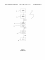
DATA
1O /
SOURCE
13 /
MEMORY
12
VERTEX
V(N+2)
V
TRANS
14 /
/
FORMATION
LIGHTING
CLIP
V(N+1
)
‘
---._-_.$§_T:HE_._--.,..
/ RENDERING
18
WW
\
/
20
DISPLAY
Figure 1
(PRIOR ART)
Patent Application Publication
Aug. 1, 2002 Sheet 2 0f 7
US 2002/0101425 A1
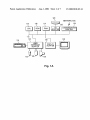
12o
110
\
116
\
CPU
ROM
é; NETWORK (135)
114
\
118
HO
RAM
ADAPTER
‘X
134
/
COMMUNICATION
ADAPTER
112
124
12%
13$
USER
'iBiii’é‘éE
132 126%
DISPLAY
128
Fig. 1A
13\8
E]
Patent Application Publication
Aug. 1, 2002 Sheet 3 0f 7
US 2002/0101425 A1
224
202
\
\
200
\‘ Shape
VGA Monitor
data on
\
ho tPC
s
x n m‘:
220
J
DAC 4
_
/
\-/
t
I
218
,>/
Co-ord
transform
-> Span
rendering
¢ Sync
generator
FPGA
X
210
K
21 6
204
Fig. 2
Patent Application Publication
Aug. 1, 2002 Sheet 4 0f 7
US 2002/0101425 A1
300
K‘
I
RECEIVING GRAPHICS DATA AND A COMMAND INDICATING A
TYPE OF OPERATIONTO BE CARRIED OUT ON THE GRAPHICS
DATA
INTEGER ALGORITHM
302
304
FLOATING POINT ALGORITHM
OR AN INTEGER ?
FLOATING POINT
ALGORITHM
V
EXECUTING THE OPERATION ON
THE GRAPHICS DATA UTILIZING A
SECOND CIRCUIT
308
EXECUTING THE OPERATIONON
THE GRAPHICS DATA UTILIZING A
FIRST CIRCUIT
Fig. 3
306
Patent Application Publication
Aug. 1, 2002 Sheet 5 0f 7
US 2002/0101425 A1
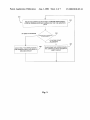
400
V
402
RECEIVING GRAPHICS DATA AND A COMMAND INDICATING A
TYPE OF OPERATIONTO BE CARRIED OUT ON THE GMPHICS
DATA
YES
404
HO CAPABILITIES
REQUIRED?
V
EXECUTING THE OPERATION ON
THE GRAPHICS DATA UTILIZING A
SECOND CIRCUIT
‘
408
EXECUT'NG THE OPERAT'ONON
THE GRAPH'CS DATA UT'L'Z'NG A
FIRST CIRCUIT
Fig. 4
406
J
Patent Application Publication
Aug. 1, 2002 Sheet 6 0f 7
US 2002/0101425 A1
macro expr HSync (x) = (x>=HSyncStartCol && x<HSyncEndCol) ;
macro expr VSync (y) = (y>=VSyncStartLine && y<VSyncEndLine) ,
interface bus_out () HSyncOut (HSync(ScanX) ) with {data = HSyncPin} ;
interface bus_out () VSyncOut (VSync(ScanY) ) with {data = VSyncPin};
while (1)
if (EndLine(ScanX) )
/*
* Reached the end of the line
* Reset x and increment y
*/
par
{
ScanX
(unsigned (log2c'ei1(TotalCols) ) ) O;
ScanY - EndScan(ScanY)
? (unsigned (log2cei1 (TotalLines) ) ) D :
ScanY-l-l;
else
{
ScanX = ScanX + 1;
}
Fig. 5
Patent Application Publication
Aug. 1, 2002 Sheet 7 0f 7
US 2002/0101425 A1
par
{
/~x
* Calculate colour
*/
whi1e(1)
{
if (ScanX>=NextStartX && ScanX[9] ==O)
/*
* Need to start the next span
*/
par
Colour = ColourBuff [SpanCount] @
(unsigned COLOUR_FRACTION_BITS) 0 ,
COlStep = ColourStep [SpanCounc] ,
NextStartX = StartX[SpanCount1 ,
SpanCount++;
}
}
else
{
[4:
* Continue with current span
*/
Colour += (unsigned)adjs ( (int) ColStep, width?iolour) ) ;
}
}
/*
* Output video
*/
while (1)
{
if (ScanY<48 i i ScanY>43l I | ScanX>5l1)
{
/~k
* Outside visible region — must be black
*/
Video = O;
}
else
{
/*
* Inside visible region - look up colour
*/
Video = ColourLUT [Colour \\ COLOUR_FRACTION_BITS1 ;
}
}
}
Aug. 1, 2002
US 2002/0101425 A1
SYSTEM, METHOD AND ARTICLE OF
MANUFACTURE FOR INCREASED I/O
CAPABILITIES IN A GRAPHICS PROCESSING
of a digital signal processor. Initially, graphics data and a
FRAMEWORK
FIELD OF THE INVENTION
Whether the operation requires I/O capabilities. If the opera
tion does not require I/O capabilities, the operation is
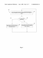
[0001] The present invention relates to graphics process
ing systems and more particularly to I/O capabilities of
operation is executed on the graphics data utiliZing a second
graphics processing systems.
BACKGROUND 0F THE INVENTION
[0002] Rendering
and displaying three-dimensional
graphics typically involves many calculations and compu
command are received indicating a type of operation to be
carried out on the graphics data. Next, it is determined
executed on the graphics data utiliZing a ?rst circuit. On the
other hand, if the operation requires I/O capabilities, the
circuit. In one embodiment, the second circuit includes a
programmable gate array.
BRIEF DESCRIPTION OF THE DRAWINGS
tations. For example, to render a three dimensional object, a
set of coordinate points or vertices that de?ne the object to
be rendered must be formed. Vertices can be joined to form
thereof Such description makes reference to the annexed
polygons that de?ne the surface of the object to be rendered
draWings Wherein:
and displayed. Once the vertices that de?ne an object are
formed, the vertices must be transformed from an object or
model frame of reference to a World frame of reference and
?nally to tWo-dimensional coordinates that can be displayed
on a ?at display device. Along the Way, vertices may be
[0007]
The invention Will be better understood When con
sideration is given to the folloWing detailed description
[0008]
FIG. 1 illustrates a prior art graphics pipeline;
[0009] FIG. 1A is a schematic diagram of a hardWare
implementation of one embodiment of the present invention;
rotated, scaled, eliminated or clipped because they fall
outside the vieWable area, lit by various lighting schemes,
[0010]
coloriZed, and so forth. Thus the process of rendering and
displaying a three-dimensional object can be computation
ally intensive and may involve a large number of vertices.
[0011] FIG. 3 illustrates a method for accelerating graph
ics operations during use of a digital signal processor;
[0003] A general system that implements a graphics pipe
modi?ed graphics pipeline of FIG. 2 improves graphics
line system is illustrated in Prior Art FIG. 1. In this system,
processing;
data source 10 generates a stream of expanded vertices
de?ning primitives. These vertices are passed one at a time,
through pipelined graphic system 12 via vertex memory 13
for storage purposes. Once the expanded vertices are
received from the vertex memory 13 into the pipelined
graphic system 12, the vertices are transformed and lit by a
transformation module 14 and a lighting module 16, respec
tively, and further clipped and set-up for rendering by a
rasteriZer 18, thus generating rendered primitives that are
FIG. 2 illustrates a modi?ed graphics pipeline, in
accordance With one embodiment of the present invention;
[0012]
FIG. 4 illustrates another method by Which the
[0013] FIG. 5 illustrates the code associated With the
synchroniZation pulse generator of the second circuit to
illustrate the simplicity of I/O management using Handel-C
and FPGAs; and
[0014] FIG. 6 illustrates the details of the core loop
associated With the span rendering module of the second
circuit.
stored in a frame buffer and then displayed on display device
20.
DETAILED DESCRIPTION OF THE
PREFERRED EMBODIMENTS
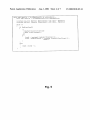
[0004] During operation, the transform module 14 may be
[0015] Apreferred embodiment of a system in accordance
With the present invention is preferably practiced in the
used to perform scaling, rotation, and projection of a set of
three dimensional vertices from their local or model coor
dinates to the tWo dimensional WindoW that Will be used to
context of a personal computer such as an IBM compatible
color and appearance of a vertex based on various lighting
personal computer, Apple Macintosh computer or UNIX
based Workstation. A representative hardWare environment
is depicted in FIG. 1A, Which illustrates a typical hardWare
schemes, light locations, ambient light levels, materials, and
con?guration of a Workstation in accordance With a pre
display the rendered object. The lighting module 16 sets the
so forth. The rasteriZation module 18 rasteriZes or renders
ferred embodiment having a central processing unit 110,
vertices that have previously been transformed and/or lit.
The rasteriZation module 18 renders the object to a rendering
such as a microprocessor, and a number of other units
interconnected via a system bus 112. The Workstation shoWn
target Which can be a display device or intermediate hard
in FIG. 1A includes a Random Access Memory (RAM) 114,
Ware or softWare structure that in turn moves the rendered
Read Only Memory (ROM) 116, an I/O adapter 118 for
data to a display device.
connecting peripheral devices such as disk storage units 120
to the bus 112, a user interface adapter 122 for connecting
[0005] Traditionally, each of the foregoing components is
implemented using application speci?c integrated circuits.
While such implementations afford increased speed, the
integrated circuits must still multi-task by performing
numerous different computations utiliZing the same hard
Ware. This may lead to sloWer processing rates, especially
When handling I/O.
SUMMARY OF THE INVENTION
a keyboard 124, a mouse 126, a speaker 128, a microphone
132, and/or other user interface devices such as a touch
screen (not shoWn) to the bus 112, communication adapter
134 for connecting the Workstation to a communication
netWork (e.g., a data processing netWork) and a display
adapter 136 for connecting the bus 112 to a display device
138. The Workstation typically has resident thereon an
operating system such as the Microsoft WindoWs NT or
A system, method and article of manufacture are
Windows/95 Operating System (OS), the IBM OS/2 oper
provided for affording enhanced I/O capabilities during use
ating system, the MAC OS, or UNIX operating system.
[0006]
Aug. 1, 2002
US 2002/0101425 A1
Those skilled in the art Will appreciate that the present
invention may also be implemented on platforms and oper
ating systems other than those mentioned.
[0016] Resident on the Workstation is a graphics pipeline
similar to that shoWn in FIG. 1. It should be noted that such
graphics pipeline may vary per the desires of the user. The
[0023] (2) Input/Output Blocks (IOB’s) are provided for
interconnecting other internal circuit components of the
FPGA device With external circuitry. The IOB’s‘ may have
?xed con?gurations or they may be con?gurable in accor
dance With user-provided con?guration instructions stored
in the con?guration-de?ning memory means.
present invention enhances such graphics pipeline for the
[0024] (3) Con?gurable Logic Blocks (CLB’s) are pro
purpose of further accelerating graphics processing during
vided for carrying out user-programmed logic functions as
de?ned by user-provided con?guration instructions stored in
use.
the con?guration-de?ning memory means.
[0017]
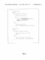
FIG. 2 illustrates a modi?ed graphics pipeline, in
accordance With one embodiment of the present invention.
As shoWn, the pipeline includes a ?rst circuit 200 that
receives graphics data 202. Such ?rst circuit 200 includes a
transform module 204, a span converter module 206, and
random access memory (RAM) 208. The operation of such
modules Will be set forth hereinafter in greater detail. In one
embodiment, the ?rst circuit 200 includes an Alex Computer
Systems Inc APAC509 SHARCPAC module. It should be
noted, hoWever, that other digital signal processors may be
utiliZed per the desires of the user.
[0018] Coupled to the ?rst circuit 200 is a second circuit
210 With a ?rst-in ?rst-out (FIFO) buffer 212 therebetWeen.
The second circuit 210 includes a span buffering module
214, a span rendering module 216, and a synchroniZation
generator 218. The operation of such modules Will be set
forth hereinafter in greater detail. The second circuit 210
feeds output to a digital to analog converter (DAC) 220
Which in turn drives a monitor 222.
[0019]
In operation, the second circuit 210 of?oads the
?rst circuit 200 and the rest of the graphics pipeline in a
manner that Will soon be set forth for the purpose of
accelerating graphics processing. In one embodiment, the
second circuit 210 includes a ?eld programmable gate array
(FPGA) device. Use of such device provides ?exibility in
[0025] Typically, each of the many CLB’s of an FPGA has
at least one lookup table (LUT) that is user-con?gurable to
de?ne any desired truth table,—to the extent alloWed by the
address space of the LUT. Each CLB may have other
resources such as LUT input signal pre-processing resources
and LUT output signal post-processing resources. Although
the term ‘CLB’ Was adopted by early pioneers of FPGA
technology, it is not uncommon to see other names being
given to the repeated portion of the FPGA that carries out
user-programmed logic functions. The term, ‘LAB’ is used
for example in US. Pat. No. 5,260,611 to refer to a repeated
unit having a 4-input LUT.
[0026] (4) An interconnect netWork is provided for carry
ing signal traffic Within the FPGA device betWeen various
CLB’s and/or betWeen various IOB’s and/or betWeen vari
ous IOB’s and CLB’s. At least part of the interconnect
netWork is typically con?gurable so as to alloW for pro
grammably-de?ned routing of signals betWeen various
CLB’s and/or IOB’s in accordance With user-de?ned routing
instructions stored in the con?guration-de?ning memory
means.
[0027] In some instances, FPGA devices may additionally
include embedded volatile memory for serving as scratchpad
memory for the CLB’s or as FIFO or LIFO circuitry. The
functionality, While maintaining high processing speeds.
embedded volatile memory may be fairly siZable and can
have 1 million or more storage bits in addition to the storage
[0020]
bits of the device’s con?guration memory.
Examples of such FPGA devices include the
XC2000TM and XC3000TM families of FPGA devices intro
duced by Xilinx, Inc. of San Jose, Calif. The architectures of
these devices are exempli?ed in US. Pat. Nos. 4,642,487;
4,706,216; 4,713,557; and 4,758,985; each of Which is
originally assigned to Xilinx, Inc. and Which are herein
incorporated by reference for all purposes. It should be
noted, hoWever, that FPGA’s of any type may be employed
in the context of the present invention.
[0021]
An FPGA device can be characteriZed as an inte
grated circuit that has four major features as folloWs.
[0022] (1) A user-accessible, con?guration-de?ning
memory means, such as SRAM, PROM, EPROM,
EEPROM, anti-fused, fused, or other, is provided in the
FPGA device so as to be at least once-programmable by
device users for de?ning user-provided con?guration
instructions. Static Random Access Memory or SRAM is of
course, a form of reprogrammable memory that can be
differently programmed many times. Electrically Erasable
and reProgrammable ROM or EEPROM is an example of
[0028] Modern FPGA’s tend to be fairly complex. They
typically offer a large spectrum of user-con?gurable options
With respect to hoW each of many CLB’s should be con?g
ured, hoW each of many interconnect resources should be
con?gured, and/or hoW each of many IOB’s should be
con?gured. This means that there can be thousands or
millions of con?gurable bits that may need to be individu
ally set or cleared during con?guration of each FPGA
device.
[0029] Rather than determining With pencil and paper hoW
each of the con?gurable resources of an FPGA device
should be programmed, it is common practice to employ a
computer and appropriate FPGA-con?guring softWare to
automatically generate the con?guration instruction signals
that Will be supplied to, and that Will ultimately cause an
unprogrammed FPGA to implement a speci?c design. (The
con?guration instruction signals may also de?ne an initial
state for the implemented design, that is, initial set and reset
states for embedded ?ip ?ops and/or embedded scratchpad
nonvolatile reprogrammable memory. The con?guration
memory cells.)
de?ning memory of an FPGA device can be formed of
mixture of different kinds of memory elements if desired
[0030] The number of logic bits that are used for de?ning
the con?guration instructions of a given FPGA device tends
(e.g., SRAM and EEPROM) although this is not a popular
to be fairly large (e.g., 1 Megabits or more) and usually
approach.
groWs With the siZe and complexity of the target FPGA.
Aug. 1, 2002
US 2002/0101425 A1
Time spent in loading con?guration instructions and veri
and/or of loading con?guration instructions from such an
fying that the instructions have been correctly loaded can
optical/magnetic form of nonvolatile memory can be toler
ated—then the optical/magnetic memory device can be used
become signi?cant, particularly When such loading is carried
out in the ?eld.
as a nonvolatile con?guration restoration means that redun
[0031]
dantly stores the con?guration data and is used to reload the
same into the system’s FPGA device(s) during poWer-up
For many reasons, it is often desirable to have
in-system reprogramming capabilities so that recon?gura
tion of FPGA’s can be carried out in the ?eld.
[0032] FPGA devices that have con?guration memories of
the reprogrammable kind are, at least in theory, ‘in-system
operations (and/or other restoration cycles).
[0039] On the other hand, if the FPGA device(s) resides in
a relatively small system that does not have such optical/
magnetic devices, and/or if the latency of loading con?gu
possibility eXists for changing the con?guration instructions
ration memory data from such an optical/magnetic device is
not tolerable, then a smaller and/or faster con?guration
Within the FPGA device While the FPGA device is ‘in
restoration means may be called for.
system’ because the con?guration memory is inherently
reprogrammable. The term, ‘in-system’ as used herein indi
[0040] Many end-use systems such as cable-TV set tops,
satellite receiver boXes, and communications sWitching
cates that the FPGA device remains connected to an appli
boXes are constrained by prespeci?ed design limitations on
programmable’ (ISP). This means no more than that a
cation-speci?c printed circuit board or to another form of
end-use system during reprogramming. The end-use system
is of course, one Which contains the FPGA device and for
Which the FPGA device is to be at least once con?gured to
operate Within in accordance With prede?ned, end-use or ‘in
the ?eld’ application speci?cations.
[0033] The possibility of recon?guring such inherently
reprogrammable FPGA’s does not mean that con?guration
changes can alWays be made With any end-use system. Nor
does it mean that, Where in-system reprogramming is pos
sible, that recon?guration of the FPGA can be made in
timely fashion or convenient fashion from the perspective of
the end-use system or its users. (Users of the end-use system
can be located either locally or remotely relative to the
end-use system.)
[0034] Although there may be many instances in Which it
is desirable to alter a pre-eXisting con?guration of an ‘in the
?eld’ FPGA (With the alteration commands coming either
from a remote site or from the local site of the FPGA), there
are certain practical considerations that may make such
in-system reprogrammability of FPGA’s more dif?cult than
?rst apparent (that is, When conventional techniques for
FPGA recon?guration are folloWed).
[0035] A popular class of FPGA integrated circuits (IC’s)
relies on volatile memory technologies such as SRAM
(static random access memory) for implementing on-chip
con?guration memory cells. The popularity of such volatile
memory technologies is oWed primarily to the inherent
reprogrammability of the memory over a device lifetime that
can include an essentially unlimited number of reprogram
ming cycles.
[0036] There is a price to be paid for these advantageous
features, hoWever. The price is the inherent volatility of the
con?guration data as stored in the FPGA device. Each time
poWer to the FPGA device is shut off, the volatile con?gu
ration memory cells lose their con?guration data. Other
events may also cause corruption or loss of data from
volatile memory cells Within the FPGA device.
physical siZe and/or poWer-up timing and/or security provi
sions and/or other provisions such that they cannot rely on
magnetic or optical technologies (or on netWork/satellite
doWnloads) for performing con?guration restoration. Their
designs instead call for a relatively small and fast acting,
non-volatile memory device (such as a securely-packaged
EPROM IC), for performing the con?guration restoration
function. The small/fast device is eXpected to satisfy appli
cation-speci?c criteria such as: (1) being securely retained
Within the end-use system; (2) being able to store FPGA
con?guration data during prolonged poWer outage periods;
and (3) being able to quickly and automatically re-load the
con?guration instructions back into the volatile con?gura
tion memory (SRAM) of the FPGA device each time poWer
is turned back on or another event calls for con?guration
restoration.
[0041] The term ‘CROP device’ Will be used herein to
refer in a general Way to this form of compact, nonvolatile,
and fast-acting device that performs ‘Con?guration-Restor
ing On PoWer-up’ services for an associated FPGA device.
[0042] Unlike its supported, volatilely reprogrammable
FPGA device, the corresponding CROP device is not vola
tile, and it is generally not ‘in-system programmable’.
Instead, the CROP device is generally of a completely
nonprogrammable type such as exempli?ed by mask-pro
grammed ROM IC’s or by once-only programmable, fuse
based PROM IC’s. Examples of such CROP devices include
a product family that the XilinX company provides under the
designation ‘Serial Con?guration PROMs’ and under the
trade name, XC1700D. TM. These serial CROP devices
employ one-time programmable PROM (Programmable
Read Only Memory) cells for storing con?guration instruc
tions in nonvolatile fashion.
[0043] Apreferred embodiment is Written using Handel-C.
Handel-C is a programming language marketed by CeloXica
Limited. Handel-C is a programming language that enables
a softWare or hardWare engineer to target directly FPGAs
(Field Programmable Gate Arrays) in a similar fashion to
classical microprocessor cross-compiler development tools,
Without recourse to a HardWare Description Language.
[0037]
Some form of con?guration restoration means is
needed to restore the lost data When poWer is shut off and
then re-applied to the FPGA or When another like event calls
for con?guration restoration (e.g., corruption of state data
Within scratchpad memory).
[0038] The con?guration restoration means can take many
forms. If the FPGA device resides in a relatively large
system that has a magnetic or optical or opto-magnetic form
of nonvolatile memory (e.g., a hard magnetic disk)—and the
latency of poWering up such a optical/magnetic device
Thereby alloWing the designer to directly realiZe the raW
real-time computing capability of the FPGA.
[0044] Handel-C is designed to enable the compilation of
programs into synchronous hardWare; it is aimed at com
piling high level algorithms directly into gate level hard
Ware.
[0045] The Handel-C syntaX is based on that of conven
tional C so programmers familiar With conventional C Will
recogniZe almost all the constructs in the Handel-C lan
guage.
Aug. 1, 2002
US 2002/0101425 A1
[0046] Sequential programs can be Written in Handel-C
just as in conventional C but to gain the most bene?t in
dimensional scenes. Such an application is an ideal example
of Where FPGAs can help out conventional DSPs since there
performance from the target hardware its inherent parallel
are sections Which require both intensive ?oating point and
ism must be exploited.
fast ?xed point operations.
[0047] Handel-C includes parallel constructs that provide
[0055]
the means for the programmer to exploit this bene?t in his
SHARC processor) is ideally suited to ?oating point, irregu
applications. The compiler compiles and optimiZes Han
The conventional DSP (in one embodiment a
lar algorithms such as the calculation of 3D coordinates of
del-C source code into a ?le suitable for simulation or a net
solid objects. FPGAs on the other hand are suited to narroW
list Which can be placed and routed on a real FPGA.
Width data paths in integer, regular algorithms such as
rendering of tWo technologies pixels. Thus, the Work can be
split betWeen the tWo technologies exploiting the strengths
[0048] More information regarding the Handel-C pro
gramming language may be found in “EMBEDDED SOLU
TIONS Handel-C Language Reference Manual: Version
3,”“EMBEDDED SOLUTIONS Handel-C User Manual:
Version 3.0,”“EMBEDDED SOLUTIONS Handel-C Inter
facing to other language code blocks: Version 3.0,” and
“EMBEDDED SOLUTIONS Handel-C Preprocessor Ref
erence Manual: Version 2.1,” each authored by Rachel GanZ,
and published by Embedded Solutions Limited, and Which
are each incorporated herein by reference in their entirety.
Additional information may be found in a co-pending appli
cation entitled “SYSTEM, METHOD AND ARTICLE OF
MANUFACTURE FOR INTERFACE CONSTRUCTS IN
A PROGRAMMING LANGUAGE CAPABLE OF PRO
GRAMMING HARDWARE ARCHITECTURES” Which
Was ?led under attorney docket number EMB1P041, and
Which is incorporated herein by reference in its entirety.
[0049]
FIG. 3 illustrates a method 300 for accelerating
graphics operations during use of a digital signal processor.
Initially, graphics data and a command are received indicat
ing a type of operation to be carried out on the graphics data.
Note operation 302.
[0050] Thereafter, it is determined in decision 304 as to
Whether the operation is a ?oating point algorithm or an
integer algorithm. As an option, the ?oating point algorithm
may include the calculation of three-dimensional coordi
nates. Moreover, the integer algorithm may include a ren
of each Within the same application.
[0056] With their I/O ?exibility, FPGAs are also ideally
suited to providing interaction With the outside World Which
is not provided directly by a speci?c module. This can be
usefull either because no module exists Which can handle the
required I/O format or to reduce the hardWare required by
combining multiple I/O formats into one FPGA. The 1/0
capabilities of the FPGA on a graphics system such as the
APAC509 may be illustrated by generating the VGA signals
for the graphics display directly from the pins of the FPGA.
All that is required externally is a simple DAC consisting of
an R-2R resistor ladder to drive the analogue RGB signals
of the monitor.
[0057] The processing associated With various modules of
the ?rst and second circuit 200 and 210, respectively, of
FIG. 2 Will noW be set forth in greater detail.
[0058] DSP Processing (First Circuit 200)
[0059] The data 202 consisting of vertices and faces is
taken from a host PC hard disk or any other similar source
using standard APEX parallel development environment I/O
functions from Alex Computer Systems, Inc. It should be
understood that other functions may be employed in other
types of environments.
dering algorithm, the generation of synchroniZation pulses,
[0060]
and/or the generation of a video output signal.
formations and projects the 3D points into 2D space using
the coordinate transform module 204. Simple light shading
is also performed at this point by calculating the intensity at
[0051] If the operation is the ?oating point algorithm, the
operation is executed on the graphics data utiliZing the ?rst
circuit 200, as indicated in operation 306. On the other hand,
if it is decided in decision 304 that the operation is the
integer algorithm, the operation on the graphics data is
executed utiliZing the second circuit 210. Note operation
The ?rst circuit 200 then makes coordinate trans
each vertex given by a single point light source and a ?xed
ambient light.
programmable gate array.
[0061] The span converter module 206 of the ?rst circuit
200 then generates a list of depth sorted single line spans
consisting of a horiZontal starting point, a starting color and
a color gradient Which are then packed into the on-chip
[0052]
RAM 208 on the ?rst circuit 200.
308. As mentioned earlier, the second circuit 210 includes a
FIG. 4 illustrates another method 400 by Which the
modi?ed graphics pipeline of FIG. 2 improves graphics
processing. In particular, the present method 400 provides
enhanced I/O capabilities during graphics processing. Ini
tially, in operation 402, graphics data and a command is
received indicating a type of operation to be carried out on
the graphics data.
[0053] Next, it is determined Whether the operation
requires I/O capabilities in decision 404. If it is determined
that the operation does not require I/O capabilities in deci
sion 404, the operation is executed on the graphics data
utiliZing the ?rst circuit 200. Note operation 406. On the
other hand, if it is determined that the operation requires I/O
capabilities in decision 404, the operation is executed on the
graphics data utiliZing the second circuit 210. Again, the
second circuit includes a programmable gate array.
[0054]
The present invention thus provides an enhanced
real-time graphics rendering and display system for three
[0062] Simultaneously, a looped, chain DMA is used to ?ll
the FIFO 212 betWeen the ?rst circuit 200 and the second
circuit 210 from an on-chip span data buffer. The DMA
sequencer hardWare of the ?rst circuit 200 is used to ensure
that the FIFO 212 never over?oWs or becomes empty.
[0063] FPGA Processing (Second Circuit 210)
[0064] The Handel-C program on the second circuit 210
(FPGA) consists of a number of parallel tasks. This illus
trates the major advantage of using FPGAs for processing
hardWare is inherently parallel.
[0065]
One task is used to generate the VGA sync pulses
using synchroniZation pulse generator 218 of the second
circuit 210. This task consists of tWo counters—ScanX and
ScanY—and some comparisons to generate pulses at the
correct period. FIG. 5 illustrates the code associated With
Aug. 1, 2002
US 2002/0101425 Al
the synchronization pulse generator 218 of the second circuit
210 to illustrate the simplicity of I/O management using
I/O capabilities during use of a graphics processor, com
Handel-C and FPGAs.
prising:
[0066] A second task is used to read span data from the
?rst circuit 200 via the FIFO 212. This operation is per
formed during the video horiZontal blanking period so that
it does not disturb the video generation task. One scan line
of spans is buffered during one scan line of blanking
utiliZing the span buffering module 214 of the second circuit
210.
[0067] A third task generates the 18 bit per pixel video
output signal by reading the buffered spans and setting the
value on 18 FPGA pins to the correct color for the current
pixel using the ScanX and ScanY counters from the sync
generator task. FIG. 6 illustrates the details of the core loop
associated With the span rendering module 216 of the second
circuit 210.
[0068] To provide a comparison for performance measure
ment, the span rendering module 216 of the second circuit
210 has also been implemented on a single SHARC DSP
using the host PC screen to display the results. Performance
improvements depend on the shape being rendered but over
a selection of 5 shapes the FPGA gives an approximate
speed increase of 2.5 times. Coupled With this is the absence
of speci?c video hardWare or video frame buffer Which
translates into loWer component count and system cost.
[0069] While various embodiments have been described
above, it should be understood that they have been presented
by Way of example only, and not limitation. Thus, the
breadth and scope of a preferred embodiment should not be
limited by any of the above described exemplary embodi
ments, but should be de?ned only in accordance With the
folloWing claims and their equivalents.
What is claimed is:
1. A method for providing enhanced I/O capabilities
during use of a graphics processor, comprising the steps of:
(a) receiving graphics data and a command indicating a
type of operation to be carried out on the graphics data;
(b) determining Whether the operation requires I/O capa
bilities;
(c) executing the operation on the graphics data utiliZing
a ?rst circuit if the operation does not require I/O
capabilities; and
(d) executing the operation on the graphics data utiliZing
a second circuit if the operation requires I/O capabili
ties;
(e) Wherein the second circuit includes a programmable
gate array.
2. Amethod as recited in claim 1, Wherein the ?rst circuit
includes a digital signal processor.
3. A method as recited in claim 1, Wherein the program
7. A computer program product for providing enhanced
(a) computer code for receiving graphics data and a
command indicating a type of operation to be carried
out on the graphics data;
(b) computer code for determining Whether the operation
requires I/O capabilities;
(c) computer code for executing the operation on the
graphics data utiliZing a ?rst circuit if the operation
does not require I/O capabilities; and
(d) computer code for executing the operation on the
graphics data utiliZing a second circuit if the operation
requires I/O capabilities;
(e) Wherein the second circuit includes a programmable
gate array.
8. A computer program product as recited in claim 7,
Wherein the ?rst circuit includes a digital signal processor.
9. A computer program product as recited in claim 7,
Wherein the programmable gate array is programmed using
Handel-C.
10. A computer program product as recited in claim 7,
Wherein the ?rst circuit is coupled to the second circuit With
a ?rst-in-?rst-out (FIFO) buffer coupled therebetWeen.
11. A computer program product as recited in claim 7,
Wherein the programmable gate array is capable of handling
multiple I/O formats.
12. A computer program product as recited in claim 7,
Wherein the programmable gate array is coupled to a digital
to-analog converter.
13. A system for providing enhanced I/O capabilities
during use of a graphics processor, comprising:
(a) logic for receiving graphics data and a command
indicating a type of operation to be carried out on the
graphics data;
(b) logic for determining Whether the operation requires
I/O capabilities;
(c) logic for executing the operation on the graphics data
utiliZing a ?rst circuit if the operation does not require
I/O capabilities; and
(d) logic for executing the operation on the graphics data
utiliZing a second circuit if the operation requires I/O
capabilities;
(e) Wherein the second circuit includes a programmable
gate array.
14. A system as recited in claim 13, Wherein the ?rst
circuit includes a digital signal processor.
15. Asystem as recited in claim 13, Wherein the program
mable gate array is programmed using Handel-C.
mable gate array is programmed using Handel-C.
16. A system as recited in claim 13, Wherein the ?rst
circuit is coupled to the second circuit With a ?rst-in-?rst-out
4. Amethod as recited in claim 1, Wherein the ?rst circuit
is coupled to the second circuit With a ?rst-in-?rst-out
(FIFO) buffer coupled therebetWeen.
(FIFO) buffer coupled therebetWeen.
mable gate array is capable of handling multiple I/O formats.
5. A method as recited in claim 1, Wherein the program
mable gate array is capable of handling multiple I/O formats.
6. A method as recited in claim 1, Wherein the program
mable gate array is coupled to a digital-to-analog converter.
17. Asystem as recited in claim 13, Wherein the program
18. Asystem as recited in claim 13, Wherein the program
mable gate array is coupled to a digital-to-analog converter.
*
*
*
*
*