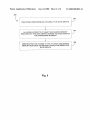
1
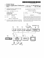
US 20020010825A1
(19) United States
(12) Patent Application Publication (10) Pub. No.: US 2002/0010825 A1
(43) Pub. Date:
Wilson
(54)
Jan. 24, 2002
MEMORY RESOURCE ARBITRATOR FOR
is a non-provisional of provisional application No.
MULTIPLE GATE ARRAYS
60/219,808, ?led on Jul. 20, 2000.
Publication Classi?cation
(76) Inventor: Alex Wilson, Oxford (GB)
Correspondence Address:
(51)
Int. Cl? ........................ .. G06F 12/00; G06F 13/14;
KEVIN J. ZILKA
PO. BOX 721120
(52)
Us. 01. ............................................................ ..710/240
G06F 13/38
SAN JOSE, CA 95172-1120 (US)
(57)
(21) Appl. No.:
(22)
Filed:
09/841,701
ABSTRACT
A system, method and computer program product for arbi
trating access to a shared memory resource by a plurality of
Apr. 23, 2001
gate arrays. During use, operations are executed on a plu
Related US. Application Data
rality of gate arrays. Further, the gate arrays are alloWed
(63) Continuation-in-part of application No. 09/687,481,
execution of the operations thereon. Such access to the at
least one shared memory resource is arbritrated to prevent
access to at least one shared memory resource during the
?led on Oct. 12, 2000. Continuation-in-part of appli
cation No. 09/687,012, ?led on Oct. 12, 2000, Which
con?ict betWeen the gate arrays.
120
NETWORK (135)
110
124
116
114
\
\
CPU ROM
RAM-l ADAPTER
112
122
\
HO
13\6
USER
111114? I
132 126
[8128
DISPLAY
118
134
/
/
COMMUNICATION
ADAPTER
138
\
Patent Application Publication
Jan. 24, 2002 Sheet 1 0f 4
US 2002/0010825 A1
120
110\
116\
@ NETWORK(135)
‘X 1/34
114\
118
/
1/0
COMMUNICATION
CFLI Roi] RAM-l ADAPTERI ADAPTER
136
\
USER
111111? |
DISPLAY
132$ 126% [8128
Fig. 1
138
P [:l
Patent Application Publication
Jan. 24, 2002 Sheet 2 0f 4
US 2002/0010825 A1
200
CPU
/
.
PARALLEL PORT
______._.__.___.__
FPGA
204
206
Fig. 2
2°8
Patent Application Publication
Jan. 24, 2002 Sheet 3 0f 4
US 2002/0010825 A1
300
K
302
EXECUTING OPERATIONS ON A PLURALITY OF GATE ARRAYS
V
304
ALLOWING ACCESS TO AT LEAST ONE SHARED MEMORY
RESOURCE BY THE GATE ARRAYS DURING THE EXECUTION OF
THE OPERATIONS THEREON
ARBIRTRATING THE ACCESS TO THE AT LEAST ONE SHARED
MEMORY RESOURCE TO PREVENT CONFLICT BETWEEN THE
GATE ARRAYS
Fig. 3
K
Patent Application Publication
Jan. 24, 2002 Sheet 4 0f 4
US 2002/0010825 A1
400
/
Filename
Purpose
Blizzard - h
MMT2000 header ?le
Fig. 4
500
Filename
Tvne
Macro Name
Purpose
Fp0server.h
Resource server
FpOserverO
Resource sewer for FPO for the
Audiorequesc.h
Audio Server
AudioRequest ()
Audio server for allowing sharing of
Flashrequest.h
Data server
FlashRequestO
Mp3request.h
MP3 server
MP3Request ()
MMT2000 lPPhone/MP3 project
sound hardware
Sewer for allowing FP1 access to the
FLASH memory
Sewer to control the MP3 application
and feed it MP3 bitstream data when
requested.
Reccnfigurerequest: .h
Fpgacomms.h
Reconfiguration
Reconfigurereq
Allows FP1 to request to be
hardware
nest ()
recon?gured, at an application exit.
Implements two unidirectional 16 bit
Communications
hardware
channels for communicating between
the two FPGAs
Fig. 5
Jan. 24, 2002
US 2002/0010825 A1
MEMORY RESOURCE ARBITRATOR FOR
MULTIPLE GATE ARRAYS
RELATED APPLICATION(S)
[0001] The present application is a continuation-in-part of
a parent application ?led Oct. 12, 2000 under Ser. No.
09/687,481, and is further a continuation-in-part of a parent
[0007] Finally, in systems having a relatively large number
of requestor lines, it is highly probable that one or more of
the requestor lines Will not be used by any of the requesters.
It has been found that under certain conditions a requestor
line Which is not connected to a requestor may temporarily
be mistaken as a requesting processor. Acknowledgement of
such “spurious” requests results in Wasted memory time and
overhead.
application ?led Oct. 12, 2000 under Ser. No. 09/687,012
Which in turn claims priority of a provisional application
?led Jul. 20, 2000 under Ser. No. 60/219,808.
[0008] It is Well knoWn that softWare-controlled machines
provide great ?exibility in that they can be adapted to many
FIELD OF THE INVENTION
different desired purposes by the use of suitable softWare. As
Well as being used in the familiar general purpose comput
[0002]
The present invention relates to resource arbitra
ers, softWare-controlled processors are noW used in many
tion and more particularly to alloWing multiple hardWare
products such as cars, telephones and other domestic prod
modules, i.e. gate arrays, to access shared resources.
ucts, Where they are knoWn as embedded systems.
BACKGROUND OF THE INVENTION
[0003] Multiprocessing techniques have become Widely
used in computing systems. Essentially, multiprocessing
systems employ a plurality of processing devices operated
[0009] HoWever, for a given a function, a softWare-con
trolled processor is usually sloWer than hardWare dedicated
to that function. AWay of overcoming this problem is to use
a special softWare-controlled processor such as a RISC
processor Which can be made to function more quickly for
substantially independent from one another to thereby
limited purposes by having its parameters (for instance siZe,
enable the computing system to simultaneously accomplish
instruction set etc.) tailored to the desired functionality.
a variety of different tasks.
[0004] Rather than provide each of the processers With a
separate mass storage memory, multiprocessing systems
generally employ a single mass storage device, such as core
memory. Each of the processors in the multiprocessing
system must therefore communicate With the single mass
storage device When a memory instruction is to be per
formed by the associated processing system. Since a single
memory may be accessed by a single requestor at any one
time, a technique must be devised for choosing betWeen tWo
or more processors Which desire to access the central
memory at the same time.
[0005] Prior art techniques for selecting the processor
have generally involved the use of discrete combinatorial
and sequential logic elements and have therefore been
highly complex and cumbersome in use. Further, such prior
art techniques are relatively in?exable in operation, thus
limiting the ability of such system to accommodate for
particular contingency. For example, in many systems, the
routine priority scheme may be upset by special memory
requests, such as a multi-cycle request Where the requesting
processor requires a memory access involving more than a
single memory cycle. Other special priority requests include
“super priority” requests such as memory refresh cycles
Which must be performed to the exclusion of all other
memory accesses. The prior art techniques employing dis
crete components cannot easily accommodate such non
routine memory requests Without involving highly complex
circuitry.
[0006] Additionally, it is important that priority assign
ments not be static in nature. That is, priorities should be
rotated on a predetermined basis such that all requesters Will
be given an equal opportunity to access memory, assuming
[0010] Where hardWare is used, though, although it
increases the speed of operation, it lacks ?exibility and, for
instance, although it may be suitable for the task for Which
it Was designed it may not be suitable for a modi?ed version
of that task Which is desired later. It is noW possible to form
the hardWare on recon?gurable logic circuits, such as Field
Programmable Gate Arrays (FPGA’s) Which are logic cir
cuits Which can be repeatedly recon?gured in different Ways.
Thus they provide the speed advantages of dedicated hard
Ware, With some degree of ?exibility for later updating or
multiple functionality.
[0011]
Varoius computer boards, such as the MMT2000®
board, are designed in such a Way that tWo FPGAs are
connected to each physical device on the board. Thus each
is individually able to drive all of the devices on the board.
HoWever, tWo main problems arise When trying to access a
resource from both FPGAs.
[0012]
In particular, the ?rst problem is related to external
memory and arises because Handel-C, a programming lan
guage for programming FPGAs, is not able to tristate the
control and address lines to external RAMs. Thus, each
RAM bank (and the FLASH memory Which shares address
pins With one of the RAM banks) can only be accessed from
one FPGA.
[0013] The second problem arises When trying to transfer
control of a device from one FPGA to the other, both
because most existing device drivers are not designed to exit
cleanly and because even if they did, most devices Would
require resetting and reinitialising every time control Was
transferred (an unnecessarily time-consuming procedure).
SUMMARY OF THE INVENTION
that such is desired. For example, if requestor 1 has priority
over requestor 2 at all times, requestor 2 Will clearly be given
less opportunity With access memory compared to requestor
[0014] A system, method and computer program product
1. The priorities must therefore be rotated over time to effect
plurality of gate arrays. During use, operations are executed
an equal distribution among the requesters. This requires
on a plurality of gate arrays. Further, the gate arrays are
for arbitrating access to a shared memory resource by a
complex sequential logic When implemented in discrete
alloWed access to at least one shared memory resource
form leading to a complex and cumbersome system.
during the execution of the operations thereon. Such access
Jan. 24, 2002
US 2002/0010825 A1
to the at least one shared memory resource is arbritrated to
parallel port 204. In one embodiment, the gate arrays are
prevent con?ict betWeen the gate arrays.
positioned on a MMT2000® dual Vertex board.
[0015] In one embodiment of the present invention, the
arbitration step avoids reinitialiZation of the device drivers
on the gate arrays. To accomplish this, the arbitration step
XC2000® and XC3000TM families of FPGA devices intro
may include locking the at least one shared memory
resource While communications are in progress With the gate
[0023]
Examples of such FPGA devices include the
duced by Xilinx, Inc. of San Jose, Calif. The architectures of
these devices are exempli?ed in US. Pat. Nos. 4,642,487;
arrays, preventing server data from being interleaved With
other data, preventing a sound driver from locking access to
the at least one shared memory, and/or controlling a graphi
4,706,216; 4,713,557; and 4,758,985; each of Which is
originally assigned to Xilinx, Inc. and Which are herein
incorporated by reference for all purposes. It should be
noted, hoWever, that FPGA’s of any type may be employed
cal user interface.
in the context of the present invention.
BRIEF DESCRIPTION OF THE DRAWINGS
[0016]
The invention Will be better understood When con
sideration is given to the folloWing detailed description
thereof. Such description makes reference to the annexed
[0024]
An FPGA device can be characteriZed as an inte
grated circuit that has four major features as folloWs.
[0025] (1) A user-accessible, con?guration-de?ning
memory means, such as SRAM, PROM, EPROM,
EEPROM, anti-fused, fused, or other, is provided in the
draWings Wherein:
FPGA device so as to be at least once-programmable by
[0017] FIG. 1 is a schematic diagram of a hardWare
implementation of one embodiment of the present invention;
device users for de?ning user-provided con?guration
[0018]
FIG. 2 is a schematic diagram of one embodiment
of the present invention Where the central processing unit
interfaces With a pair of gate arrays via a parallel port;
[0019] FIG. 3 illustrates a method for arbitrating access to
a shared memory resource by a plurality of gate arrays; and
[0020] FIGS. 4 and 5 illustrate various external depen
dencies and Handel-C Macros, respectively, in accordance
With one embodiment of the present invention.
DETAILED DESCRIPTION OF THE
PREFERRED EMBODIMENTS
[0021] Apreferred embodiment of a system in accordance
With the present invention is preferably practiced in the
context of a personal computer such as an IBM compatible
personal computer, Apple Macintosh computer or UNIX
based Workstation. A representative hardWare environment
is depicted in FIG. 1, Which illustrates a typical hardWare
instructions. Static Random Access Memory or SRAM
is of course, a form of reprogrammable memory that
can be differently programmed many times. Electri
cally Erasable and reProgrammable ROM or EEPROM
is an example of nonvolatile reprogrammable memory.
The con?guration-de?ning memory of an FPGA device
can be formed of mixture of different kinds of memory
elements if desired (e.g., SRAM and EEPROM)
although this is not a popular approach.
[0026] (2) Input/Output Blocks (IOB’s) are provided
for interconnecting other internal circuit components of
the FPGA device With external circuitry. The IOB’s’
may have ?xed con?gurations or they may be con?g
urable in accordance With user-provided con?guration
instructions stored in the con?guration-de?ning
memory means.
[0027] (3) Con?gurable Logic Blocks (CLB’s) are pro
vided for carrying out user-programmed logic functions
as de?ned by user-provided con?guration instructions
stored in the con?guration-de?ning memory means.
con?guration of a Workstation in accordance With a pre
ferred embodiment having a central processing unit 110,
such as a microprocessor, and a number of other units
interconnected via a system bus 112. The Workstation shoWn
in FIG. 1 includes a Random Access Memory (RAM) 114,
Read Only Memory (ROM) 116, an I/O adapter 118 for
[0028] Typically, each of the many CLB’s of an FPGA has
at least one lookup table (LUT) that is user-con?gurable to
de?ne any desired truth table,—to the extent alloWed by the
address space of the LUT. Each CLB may have other
resources such as LUT input signal pre-processing resources
connecting peripheral devices such as disk storage units 120
to the bus 112, a user interface adapter 122 for connecting
and LUT output signal post-processing resources. Although
the term ‘CLB’ Was adopted by early pioneers of FPGA
a keyboard 124, a mouse 126, a speaker 128, a microphone
technology, it is not uncommon to see other names being
132, and/or other user interface devices such as a touch
screen (not shoWn) to the bus 112, communication adapter
134 for connecting the Workstation to a communication
netWork (e.g., a data processing netWork) and a display
adapter 136 for connecting the bus 112 to a display device
138. The Workstation typically has resident thereon an
operating system such as the Microsoft WindoWs NT or
Windows/95 Operating System (OS), the IBM OS/2 oper
ating system, the MAC OS, or UNIX operating system.
Those skilled in the art Will appreciate that the present
invention may also be implemented on platforms and oper
ating systems other than those mentioned.
[0022]
FIG. 2 is a schematic diagram of one embodiment
200 of the present invention Where the central processing
unit 110 interfaces With a pair of gate arrays 206 via a
given to the repeated portion of the FPGA that carries out
user-programmed logic functions. The term, ‘LAB’ is used
for example in US. Pat. No. 5,260,611 to refer to a repeated
unit having a 4-input LUT.
[0029] (4) An interconnect netWork is provided for
carrying signal traf?c Within the FPGA device betWeen
various CLB’s and/or betWeen various IOB’s and/or
betWeen various IOB’s and CLB’s. At least part of the
interconnect netWork is typically con?gurable so as to
alloW for programmably-de?ned routing of signals
betWeen various CLB’s and/or IOB’s in accordance
With user-de?ned routing instructions stored in the
con?guration-de?ning memory means.
[0030] In some instances, FPGA devices may additionally
include embedded volatile memory for serving as scratchpad
US 2002/0010825 A1
memory for the CLB’s or as FIFO or LIFO circuitry. The
embedded volatile memory may be fairly sizable and can
have 1 million or more storage bits in addition to the storage
J an. 24, 2002
from a remote site or from the local site of the FPGA), there
are certain practical considerations that may make such
in-system reprogrammability of FPGA’s more dif?cult than
bits of the device’s con?guration memory.
?rst apparent (that is, When conventional techniques for
[0031] Modern FPGA’s tend to be fairly complex. They
typically offer a large spectrum of user-con?gurable options
FPGA recon?guration are folloWed).
With respect to hoW each of many CLB’s should be con?g
ured, hoW each of many interconnect resources should be
con?gured, and/or hoW each of many IOB’s should be
con?gured. This means that there can be thousands or
[0038] A popular class of FPGA integrated circuits (IC’s)
relies on volatile memory technologies such as SRAM
(static random access memory) for implementing on-chip
con?guration memory cells. The popularity of such volatile
memory technologies is oWed primarily to the inherent
millions of con?gurable bits that may need to be individu
ally set or cleared during con?guration of each FPGA
device.
reprogrammability of the memory over a device lifetime that
can include an essentially unlimited number of reprogram
[0032] Rather than determining With pencil and paper hoW
[0039] There is a price to be paid for these advantageous
features, hoWever. The price is the inherent volatility of the
each of the con?gurable resources of an FPGA device
should be programmed, it is common practice to employ a
computer and appropriate FPGA-con?guring softWare to
automatically generate the con?guration instruction signals
that Will be supplied to, and that Will ultimately cause an
unprogrammed FPGA to implement a speci?c design. (The
con?guration instruction signals may also de?ne an initial
state for the implemented design, that is, initial set and reset
states for embedded ?ip ?ops and/or embedded scratchpad
memory cells.)
[0033] The number of logic bits that are used for de?ning
the con?guration instructions of a given FPGA device tends
to be fairly large (e.g., 1 Megabits or more) and usually
groWs With the siZe and complexity of the target FPGA.
Time spent in loading con?guration instructions and veri
fying that the instructions have been correctly loaded can
become signi?cant, particularly When such loading is carried
out in the ?eld.
[0034]
For many reasons, it is often desirable to have
ming cycles.
con?guration data as stored in the FPGA device. Each time
poWer to the FPGA device is shut off, the volatile con?gu
ration memory cells lose their con?guration data. Other
events may also cause corruption or loss of data from
volatile memory cells Within the FPGA device.
[0040]
Some form of con?guration restoration means is
needed to restore the lost data When poWer is shut off and
then re-applied to the FPGA or When another like event calls
for con?guration restoration (e.g., corruption of state data
Within scratchpad memory).
[0041] The con?guration restoration means can take many
forms. If the FPGA device resides in a relatively large
system that has a magnetic or optical or opto-magnetic form
of nonvolatile memory (e.g., a hard magnetic disk)—and the
latency of poWering up such a optical/magnetic device
and/or of loading con?guration instructions from such an
optical/magnetic form of nonvolatile memory can be toler
ated—then the optical/magnetic memory device can be used
in-system reprogramming capabilities so that recon?gura
as a nonvolatile con?guration restoration means that redun
tion of FPGA’s can be carried out in the ?eld.
dantly stores the con?guration data and is used to reload the
same into the system’s FPGA device(s) during poWer-up
[0035] FPGA devices that have con?guration memories of
the reprogrammable kind are, at least in theory, ‘in-system
programmable’ (ISP). This means no more than that a
possibility eXists for changing the con?guration instructions
operations (and/or other restoration cycles).
[0042] On the other hand, if the FPGA device(s) resides in
a relatively small system that does not have such optical/
Within the FPGA device While the FPGA device is ‘in
magnetic devices, and/or if the latency of loading con?gu
system’ because the con?guration memory is inherently
reprogrammable. The term, ‘in-system’ as used herein indi
ration memory data from such an optical/magnetic device is
not tolerable, then a smaller and/or faster con?guration
cates that the FPGA device remains connected to an appli
restoration means may be called for.
cation-speci?c printed circuit board or to another form of
end-use system during reprogramming. The end-use system
[0043] Many end-use systems such as cable-TV set tops,
satellite receiver boXes, and communications sWitching
is of course, one Which contains the FPGA device and for
Which the FPGA device is to be at least once con?gured to
boXes are constrained by prespeci?ed design limitations on
operate Within in accordance With prede?ned, end-use or ‘in
the ?eld’ application speci?cations.
sions and/or other provisions such that they cannot rely on
magnetic or optical technologies (or on netWork/satellite
[0036] The possibility of recon?guring such inherently
doWnloads) for performing con?guration restoration. Their
reprogrammable FPGA’s does not mean that con?guration
changes can alWays be made With any end-use system. Nor
does it mean that, Where in-system reprogramming is pos
sible, that recon?guration of the FPGA can be made in
timely fashion or convenient fashion from the perspective of
the end-use system or its users. (Users of the end-use system
can be located either locally or remotely relative to the
end-use system.)
physical siZe and/or poWer-up timing and/or security provi
designs instead call for a relatively small and fast acting,
non-volatile memory device (such as a securely-packaged
EPROM IC), for performing the con?guration restoration
function. The small/fast device is eXpected to satisfy appli
cation-speci?c criteria such as: (1) being securely retained
Within the end-use system; (2) being able to store FPGA
con?guration data during prolonged poWer outage periods;
and (3) being able to quickly and automatically re-load the
con?guration instructions back into the volatile con?gura
[0037] Although there may be many instances in Which it
tion memory (SRAM) of the FPGA device each time poWer
is desirable to alter a pre-eXisting con?guration of an ‘in the
is turned back on or another event calls for con?guration
?eld’ FPGA (With the alteration commands coming either
restoration.
Jan. 24, 2002
US 2002/0010825 A1
[0044] The term ‘CROP device’ Will be used herein to
refer in a general Way to this form of compact, nonvolatile,
and fast-acting device that performs ‘Con?guration-Restor
ing On PoWer-up’ services for an associated FPGA device.
Jan. 29, 2001 under Ser. No. 09/772,555, and Which is
incorporated herein by reference in its entirety.
[0052]
FIG. 3 illustrates a method 300 for arbitrating
access to a shared memory resource by a plurality of gate
tile, and it is generally not ‘in-system programmable’.
arrays. During use, operations are executed on a plurality of
gate arrays, as indicated in step 302. In one embodiment, the
gate arrays included FPGA’s.
Instead, the CROP device is generally of a completely
[0053] Further, in operation 304, the gate arrays are
[0045] Unlike its supported, volatilely reprogrammable
FPGA device, the corresponding CROP device is not vola
nonprogrammable type such as exempli?ed by mask-pro
grammed ROM IC’s or by once-only programmable, fuse
based PROM IC’s. Examples of such CROP devices include
a product family that the Xilinx company provides under the
designation ‘Serial Con?guration PROMs’ and under the
trade name, XC1700D.TM. These serial CROP devices
employ one-time programmable PROM (Programmable
Read Only Memory) cells for storing con?guration instruc
tions in nonvolatile fashion.
alloWed access to at least one shared memory resource
during the execution of the operations thereon. Such access
to the at least one shared memory resource is arbritrated to
prevent con?ict betWeen the gate arrays. See operation 306.
[0054] The present invention alloWs access to external
memory and FLASH from both gate arrays Whilst using the
RAM construct. Further, it provides arbitration thus prevent
ing con?icts When both FPGAs are accessing the same
resource. Also, the present invention removes the need to
[0046] Apreferred embodiment is Written using Handel-C.
stop and reinitialiZe drivers and hardWare When passing
Handel-C is a programming language marketed by Celoxica
Limited. Handel-C is a programming language that enables
from one FPGA to the other.
a softWare or hardWare engineer to target directly FPGAs
(Field Programmable Gate Arrays) in a similar fashion to
classical microprocessor cross-compiler development tools,
Without recourse to a HardWare Description Language.
Thereby alloWing the designer to directly realiZe the raW
real-time computing capability of the FPGA.
[0047] Handel-C is designed to enable the compilation of
programs into synchronous hardWare; it is aimed at com
piling high level algorithms directly into gate level hard
Ware.
[0048] The Handel-C syntax is based on that of conven
tional C so programmers familiar With conventional C Will
recogniZe almost all the constructs in the Handel-C lan
guage.
[0055] One of the key features of the MMT2000® board
includes the ability to recon?gure itself both from Flash and
over the Ethernet. It is apparent that there is a natural
division of the roles of the tWo FPGAs. One (the server, or
FPO) has access to the Flash and the NetWork and includes
the recon?guration device driver. The other (the client
application or FP1) has control over the display, touchscreen
and the audio chip.
[0056] The present invention encapsulates a bi-directional
16 bit communications driver for alloWing the tWo FPGAs
to talk to each other. Every message from one FPGA to the
other is preceded by a 16 bit ID, the high eight bits of Which
identify the type of message (AUDIO, FLASH, RECON
FIGURATION etc . . . ) and the loW identify the particular
request for that hardWare (FLASH_READ etc . . .
The
identi?er codes are processed in a header ?le (e.g.
[0049] Sequential programs can be Written in Handel-C
just as in conventional C but to gain the most bene?t in
performance from the target hardWare its inherent parallel
ism must be exploited.
[0050] Handel-C includes parallel constructs that provide
the means for the programmer to exploit this bene?t in his
applications. The compiler compiles and optimiZes Han
del-C source code into a ?le suitable for simulation or a net
“fp0server.h” in the context of the Handel-C programming
language), and then an appropriate macro procedure is called
for each type of message (eg for AUDIOQAudioRequest)
Which then receives and processes the main body of the
communication.
[0057] The server process requires a number of parameters
to be passed to it. Such parameters Will noW be set forth.
list Which can be placed and routed on a real FPGA.
[0058] PID: Used for locking shared resources (such as
the FLASH) from other processes While communica
[0051] More information regarding the Handel-C pro
gramming language may be found in “EMBEDDED SOLU
TIONS Handel-C Language Reference Manual: Version
[0059] usendCommand, uSendLock: A channel alloW
3,”“EMBEDDED SOLUTIONS Handel-C User Manual:
Version 3.0,”“EMBEDDED SOLUTIONS Handel-C Inter
facing to other language code blocks: Version 3.0,” each
authored by Rachel GanZ, and published by Celoxica Lim
ited in the year of 2001; and “EMBEDDED SOLUTIONS
Handel-C Preprocessor Reference Manual: Version 2.1,”
also authored by Rachel GanZ and published by Embedded
Solutions Limited in the year of 2000; and Which are each
incorporated herein by reference in their entirety. Additional
information may also be found in a co-pending application
entitled “SYSTEM, METHOD AND ARTICLE OF MANU
FACTURE FOR INTERFACE CONSTRUCTS IN A PRO
GRAMMING LANGUAGE CAPABLE OF PROGRAM
MING HARDWARE ARCHITECTURES” Which Was ?led
tions are in progress.
ing applications on FPO to send commands to applica
tions on FP1 and a one-bit locking variable to ensure
the data is not interleaved With server-sent data.
[0060] uSoundOut, uSoundIn: TWo channels mirroring
the function of the audio driver. Data sent to uSound
Out Will be played (assuming the correct code in FP1)
out of the MMT2000® speakers, and data read from
uSoundIn is the input to the MMT2000® microphone.
The channels are implemented in such a Way that When
the sound driver blocks, the communication channel
betWeen FPGAs is not held up.
[0061]
MP3Run: A one bit variable controlling the MP3
GUI. The server Will activate or deactivate the MP3
GUI on receipt of commands from FP1.
Jan. 24, 2002
US 2002/0010825 A1
[0062] Con?gAddr: A 23 bit channel controlling the
(b) computer code for alloWing access to at least one
recon?guration process. When the ?ash address of a
valid FPGA bit?le is sent to this channel, the server
shared memory resource by the gate arrays during the
execution of the operations thereon; and
recon?gures FP1 With the bitmap speci?ed.
[0063] During use, the data transfer rate betWeen the tWo
FPGAs in either direction is 16 bits per 5 clock cycles (in the
clock domain of the sloWest FPGA). This is the maximum
possible reliable rate for communicating betWeen FPGAs
that may be running at different clock rates. FIGS. 4 and 5
illustrate various external dependencies 400 and Handel-C
Macros 500, respectively, in accordance With one embodi
ment of the present invention. Note Appendix A.
[0064] While various embodiments have been described
above, it should be understood that they have been presented
by Way of example only, and not limitation. Thus, the
breadth and scope of a preferred embodiment should not be
limited by any of the above described exemplary embodi
ments, but should be de?ned only in accordance With the
folloWing claims and their equivalents.
What is claimed is:
1. A method for arbitrating access to a shared memory
resource by a plurality of gate arrays, comprising the steps
of:
(a) executing operations on a plurality of gate arrays;
(b) alloWing access to at least one shared memory
resource by the gate arrays during the execution of the
operations thereon; and
(c) arbirtrating the access to the at least one shared
memory resource to prevent con?ict betWeen the gate
arrays.
2. A method as recited in claim 1, Wherein arbitration step
avoids reinitialiZation of the device drivers on the gate
arrays.
3. A method as recited in claim 1, Wherein the arbitration
step includes locking the at least one shared memory
resource While communications are in progress With the gate
arrays.
4. A method as recited in claim 1, Wherein the arbitration
step includes preventing server data from being interleaved
With other data.
5. A method as recited in claim 1, Wherein the arbitration
step includes preventing a sound driver from locking access
to the at least one shared memory resource.
6. A method as recited in claim 1, Wherein the arbitration
step includes controlling a graphical user interface.
7. A computer program product for arbitrating access to a
shared memory resource by a plurality of gate arrays,
comprising:
(a) computer code for executing operations on a plurality
of gate arrays;
(c) computer code for arbirtrating the access to the at least
one shared memory resource to prevent con?ict
betWeen the gate arrays.
8. A computer program product as recited in claim 7,
Wherein arbitration step avoids reinitialiZation of the device
drivers on the gate arrays.
9. A computer program product as recited in claim 7,
Wherein the arbitration step includes locking the at least one
shared memory resource While communications are in
progress With the gate arrays.
10. A computer program product as recited in claim 7,
Wherein the arbitration step includes preventing server data
from being interleaved With other data.
11. A computer program product as recited in claim 7,
Wherein the arbitration step includes preventing a sound
driver from locking access to the at least one shared memory
resource.
12. A computer program product as recited in claim 7,
Wherein the arbitration step includes controlling a graphical
user interface.
13. A system for arbitrating access to a shared memory
resource by a plurality of gate arrays, comprising:
(a) logic for executing operations on a plurality of gate
arrays;
(b) logic for alloWing access to at least one shared
memory resource by the gate arrays during the execu
tion of the operations thereon; and
(c) logic for arbirtrating the access to the at least one
shared memory resource to prevent con?ict betWeen
the gate arrays.
14. A system as recited in claim 13, Wherein arbitration
step avoids reinitialiZation of the device drivers on the gate
arrays.
15. A system as recited in claim 13, Wherein the arbitra
tion step includes locking the at least one shared memory
resource While communications are in progress With the gate
arrays.
16. A system as recited in claim 13, Wherein the arbitra
tion step includes preventing server data from being inter
leaved With other data.
17. A system as recited in claim 13, Wherein the arbitra
tion step includes preventing a sound driver from locking
access to the at least one shared memory resource.
18. A system as recited in claim 13, Wherein the arbitra
tion step includes controlling a graphical user interface.