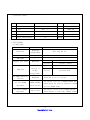
1
SERVICE
MANUAL
Model
1. PMCP642(NP-42H4B9)
2. PMCP650(NP-50H4D9)
3. PMCP660(NP-60H4G9)
CONFIDENTIALITY
All material contained within this document is proprietary information and the
sole
property of WoosungNextier Corp. #821~3, Byucksan Digital ValleyⅡ, 481-10,
gasan-dong, Geumcheon-Gu, Seoul-city, Korea.
No part of this document may be copied, reproduced, or transmitted by any
means, for any purpose without prior written permission from WoosungNextier
Corp.
Service Manual Revision
Date
Description
By
Approved
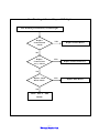
CONTENTS
◆ SPECIFICATION
◆ ENGINEERING SPECIFICATION
◆ BLOCK DIAGRAM
◆ CIRCUIT
◆ EXPLODED VIEW
◆ CALIBRATION METHODS
◆ INSPECTION METHODS
◆ FIRMWARE UPGRADE METHOD
◆ SERIAL CONTROL PROTOCOLS
◆ TROUBLE SHOOTING
◆ PDP MODULE SERVICE MANUAL
Specifications for PDP Monitor(9-BNC)
Model : PMCP642(NP-42H4B9)
PMCP650(NP-50H4D9)
PMCP660(NP-60H4G9)
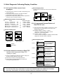
Main Features
● Pixelworks DNX™ (Digital Natural Expression) technology including
Pixelworks DNX™ (Digital Natural Expression) technology
dramatically enhances the quality of video images
by combining multiple Pixelworks video processing technologies
to deliver clear,natural-looking standard and high-definition video images.
DNX technology combines sophisticated digital video processing techniques,
advanced scaling,motion-adaptive deinterlacing,noise reduction,
dynamic edge enhancement,and smoothing of moving lines to deliver a lifelike picture.
●
●
●
●
●
●
●
●
●
●
●
•
•
•
•
•
•
•
•
•
•
•
•
•
•
High Brightness and High Contrast Ratio
DVI(Digital Visual Interface) Support Up to 720p , 1080i , 1280x1024 / 60 Hz(SXGA),
HDCP(High-bandwidth Digital Content Protection) Supported
Multi-Standard RGB(PC) Monitor Support Up to 720p , 1080i , 1280x1024 / 60 Hz (SXGA),
Multi-Standard Component Signal Compatibility : 480i , 576i , 480p , 576p , 720p , 1080i
Multi-Standard Video System Supported : NTSC , PAL , SECAM
Multi-screen display : Normal , PiP, PBP
Variable Image size : Auto,Fill All(16:9),Fill Aspect,Zoom,Anamorphic,Wide
Variable Picture control : Brightness , Contrast , Sharpness , Color , Tint
Variable Audio control : Volume , Mute , Bass , Treble , Balance
Video Enhancement features including
DCTI(Digital Chroma Transient) / DLTI(Digital Luminance Transient Improvement)
Digital luminance peaking and Horizontal Peaking
Enhanced sharpness controls
Advanced Noise Reduction including progressive sources
Flesh Tone Correction (FTC)
Chroma Upsampling Error (CUE) correction
Improved White and Black-level expansion
Digital 3D Comb-filter
Digital brightness, contrast, hue, and saturation control
PixelBoost™(Pixelworks) overdrive technology for video format
Improved scaler and filters for sharper images
Improved multi-region, anamorphic scaling for 4:3<->16:9 aspect ratio conversion
Independent vertical and horizontal scalers
True 10-bit(1 billion color) processing (Option)
● Deinterlacing features including
•
•
•
•
Improved deinterlacer, supporting SDTV and HDTV, for standard NTSC/PAL/SECAM,1080i
Per-pixel motion-compensated deinterlacing
Improved Low-Angle Interpolation
Film mode for 3:2/2:2 pull-down materials, including 1080i sources
● Audio Enhancement features including
•
•
•
•
●
●
●
●
●
●
Automatic Volume Correction (AVC)
Audio Delay for "Lip Sync" (Option)
Spatial Effects
Pseudo Stereo
Multi-Language On Screen Display (OSD)
Still image function
Image Sticking Minimum Function
Sleep Timer
Close Caption support
Ultra slim & light design
1/3
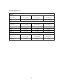
PDP Monitor
Specifications
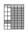
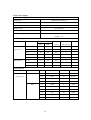
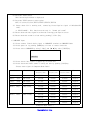
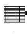
Item
Display
PMCP642
(NP-42H4B9)
Screen Size(Active Area)
Aspect ratio
Number of Pixels
Pixel Pitch
Displayable Colors
Brightness
Contrast Ratio
Color Temperature
RS-232C
DVI
Input
RGB
Input
In / Out
Terminals
Component
Input
Over 160 degrees
10W(L) + 10W(R) [RMS] / 8 Ω
2 Way 2 Speaker
Internal Speaker
10W(L) + 10W(R) [RMS] / 8 Ω
2 Way 4 Speaker System
Digital RGB : TMDS
MAX : 720p , 1080i , 1280 x 1024 / 60 Hz (SXGA)
RCA Jack x 1
Audio : 0.5V[rms](Normal) / 2 Channel (L+R)
D-Sub Jack x 1
(15 pin)
Analog RGB : 0.7V[p-p](75Ω), H/CS/V : TTL (2.2 kΩ), SOG : 1V[p-p](75Ω)
MAX : 720p , 1080i , 1280 x 1024 / 60 Hz (SXGA)
RCA Jack x 1
Audio : 0.5V[rms](Normal) / 2 Channel (L+R)
RCA Jack x 1
Y:1V[p-p](75Ω) , Pb/Cb:0.7V[p-p](75Ω) , Pr/Cr:0.7V[p-p](75Ω)
480i , 576i , 480p , 576p , 720p , 1080i
Audio : 0.5V[rms](Normal) / 2 Channel (L+R)
TXD + RXD (1:1)
Monitor
Output
BNC Jack x 1
Video : 1V[p-p] ( 75 Ω)
RCA Jack x 1
Audio : 0.5V[rms](Normal) / 2 Channel (L + R)
S-Video
Input
Mini DIN Jack x1 Y: 1V[p-p] ( 75 Ω) , C: 0.286V[p-p] ( 75 Ω) [NTSC]
(4 pin)
Y: 1V[p-p] ( 75 Ω) , C: 0.300V[p-p] ( 75 Ω) [PAL / SECAM]
Video
Input
BNC Jack x 1
Video : 1V[p-p] ( 75 Ω) [ NTSC / PAL / SECAM]
RCA Jack x 1
Audio : 0.5V[rms](Normal) / 2 Channel (L + R)
Video 1 , 2
RCA Jack x 2
Video : 1V[p-p] ( 75 Ω)
Audio : 0.5V[rms](Normal) / 2 Channel (L+R)
AC 100V ~ 240V, 50/60Hz
Power Consumption (Typical)
Dimensions (Without Stand)
[ W mm x H mm x D mm ]
350W
450W
610W
1028 x 625 x 107.4
1206.7 x 721 x117.3
1454 x 876 x 94.1
30 kg
42 kg
0 ~ 40 ℃
-20 ~ 60 ℃
20 ~ 80% RH (No condensation)
10 ~ 90% RH (NO condensation)
800 ~ 1100 hPa (Altitude : 0 ~ 2,000 m)
700 ~ 1100 hPa (Altitude : 0 ~ 3,000 m)
67.3 kg
Weight (Without Stand)
Environmen
t
Condition
10W(L) + 10W(R) [RMS] / 8 Ω
2 Way 6 Speaker System
External Speaker
(Option)
D-Sub Jack x 1
(9 pin)
DVI Jack x 1
(24 pin)
Power Supply
General
PMCP660
(NP-60H4G9)
42" (920.1(H) x 518.4(V)±0.5mm)50" (1106.5(H) x 622.1(V)±0.5mm)60" (1319.6(H) x 741.9(V)±0.5mm
16:9
1366 (H) x 768 (V)
1024 (H) x 768 (V)
1366 (H) x 768 (V)
0.966(H) x 0.966(V) [mm]
0.900(H) x 0.676(V) [mm]
0.810(H) x 0.810(V) [mm]
1 billion (Option)
1000 cd/㎡
1200 cd/㎡
1200 cd/㎡
8000:1
8000:1
7000:1
9500 K
Viewing Angle
Speaker
Output
PMCP650
(NP-50H4D9)
Operational
Temperature
Storage
Operational
Humidity
Storage
Operational
Pressure
Storage
* The specifications are subject to change without notice
2/3
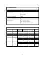
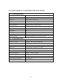
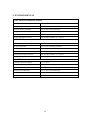
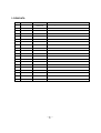
External Speaker (Option)
Specifications
Item
Dimensions (W x H x D)
Weight
Type
Input
Impedence
Output Sound Pressure
Frequency Response
42"
50"
113 mm x 626.6 mm x 82.2 mm
90 mm x 721 mm x 68 mm
5 kg ( L + R )
3 kg ( L + R )
2 Way 4 Speaker System
10 W ( RMS)
8Ω
87 dB/W/M
60"
1452mm x 123mm x 86.8mm
5 kg ( L + R )
2 Way 6 Speaker System
45 Hz ~ 20 KHz
* The specifications are subject to change without notice
Internal Speaker
Item
Specifications
42"
Type
Input
Impedence
Output Sound Pressure
Frequency Response
50"
60"
2 Way 2 Speaker
10 W ( RMS)
8Ω
88 dB/W/M
170 Hz ~20 KHz
* The specifications are subject to change without notice
Accessories
Standard
Owner's Instruction , Remote Controller/AAA Batteries , Power Cord
Foot Stand , Table-Top stand , Wall-Mount Bracket , Ceiling-Mount Bracket ,
Internal Speaker System , External Speaker System ,
Option
DVI Cable , VGA(D-SUB) Cable , Audio Cable , Component Cable ,
RCA Video Cable , RCA Audio Cable , S-Video Cable ,
* The specifications are subject to change without notice
3/3
Woosung Nextier Corp.
------------------------------------------------------------------------------------------------------------
Engineering Products Specification
MODEL
1. PMCP642(NP-42H4B9)
2. PMCP650(NP-50H4D9)
3. PMCP660(NP-60H4G9)
PDP MONITORs
■Preliminary
□Approved
Woosung Nextier Corp.
DATE :
DATE :
PELCO
Ver.1.2
11/24/06
By Tommy Shin
CONFIDENTIALITY
All material contained within this document is proprietary information and the sole
property of Woosung Nextier Corp. 481-10 Gasan-dong, Byeoksan Digital Valley II #821,
Geumcheon-gu, Seoul, Korea. No part of this document may be copied, reproduced, or
transmitted by any means, for any purpose without prior written permission from
Woosung Nextier Corp..
2
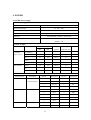
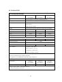
TABLE OF CONTENTS
1.
SCOPE
1.1 Introduction
2.
1.2
Product Definition
1.3
Mass Production Release
1.4
Change Control
1.5
Service
GENERAL SPECIFICATION
2.1
General Specification
2.2 Input/Output Terminal
3.
4.
INPUT SIGNAL INTERFACE
3.1
DVI Interface
3.2
RGB Interface
3.3
DVI / RGB Mode Table
3.4
Component Interface
3.5
Component Mode Table
3.6
S-Video Interface
3.7
Video Interface
POWER
4.1 42”HD Power Supply
4.1.1 Power Supply(SMPS)
4.1.2 DC Output
4.1.3 Connector
4.2 50”HD Power Supply
4.2.1 Power Supply(SMPS)
4.2.2 DC Output
4.2.3 Connector
4.3 60”HD Power Supply
4.3.1 Power Supply(SMPS)
4.3.2 DC Output
4.3.3 Connector
3
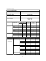
5.
6.
7.
8.
9.
CONTROLS AND INDICATORS
5.1
Hardware Control
5.2
Remote Control
5.3
Menu Control
PLASMA DISPLAY PANEL(PDP) SPECIFICATIONS
6.1
42”HD Specification
6.2
50”HD Specification
6.3
60”HD Specification
DISPLAY CELL DEFECT SPECIFICATIONS
7.1
42”HD Cell Defect Specification
7.2
50”HD Cell Defect Specification
7.3
60”HD Cell Defect Specification
MECHANICAL
8.1
Fan
8.2
Dimension(without stand)
8.3
Weight
ENVIRONMENTAL
9.1
42”HD Environmental Condition
9.2
50”HD Environmental Condition
9.3
60”HD Environmental Condition
10. PACKAGING
10.1
Packaging Specifications
10.2
Vibration
10.3
Drop
11. AUDIO SYSTEM
11.1
Internal Speaker System
12. WARRANTY
12.1
Parts and Labor
4
1. SCOPE
1.1 Introduction
Product configuration
This specification defines the configuration and performance
requirements for the following Plasma Displays.
Product Name : PDP monitors
Display Type : 42” HD / 50” HD / 60” HD
Plasma Displays
Model Name
: PMCP642 (NP-42H4B9),
PMCP650 (NP-50H4D9),
PMCP660 (NP-60H4G9)
1.2 Product Definition
The top level assembly shall contain :
1. Plasma Display : PMCP642 (NP-42H4B9),
PMCP650 (NP-50H4D9),
PMCP660 (NP-60H4G9)
2. Power Cord(USA & Europe)
3. RGB Cable
4. DVI Cable
3. Remote Control Unit
Top Level Assembly
4. “AAA” Batteries n=2
5. Installation/Operation Manual
6. Foot Stand
Optional Accessories
1. S-Video Cable
2. PC Audio Cable
3. Wall Mount Bracket
4. Wall Mount Bracket(Tilt Capable)
5
1.3 Mass Production Release
Mass Production Approval
Mass Production shall not begin until Woosung
Nextier Corp. has issued a Mass Production Release.
All exterior plastic components, screen printed components,
Component Approvals
labels, shipping cartons, protective foam, and printed
materials require approval by Woosung Nextier Corp. prior
to Mass Production Release.
1.4 Change Control
All Engineering changes to the product shall be made in
ECR/ECN
accordance with the Woosung Nextier Corp. ECR/ECN
Procedure.
1.5 Service
Complete Spare Parts List, Schematic, Service Manual, and
Documentation / Service Manual
Assembly Drawings shall be provided within one month of
Mass Production Release.
6
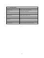
2. GENERAL SPECIFICATION
2.1 General Specification
Display Type
Model Name
Native Resolution & Frequency
42”HD
50”HD
60”HD
PMCP642
PMCP650
PMCP660
(NP-42H4B9)
(NP-50H4D9)
(NP-60H4G9)
1024 X 768 @ 60Hz
1366 X 768 @ 60Hz
1366 X 768 @ 60Hz
AC100V ~ 240V,
AC100V ~ 240V,
AC100V ~ 240V,
50/60Hz
50/60Hz
50/60Hz
Input Voltage
2.2 Input/Output Terminal
DVI Input
RGB Input
Component Input
S-Video Input
Video Input
Video1, 2 Input
Monitor Output
RS-232C
DVI-D 24-pin Jack × 1
RCA Jack(L+R) × 1
D-Sub 15-pin Jack ×1
RCA Jack(L+R) × 1
RCA(YPbPr/YCbCr) Jack × 1
RCA(L+R) Jack × 1
Mini DIN S-terminal × 1
BNC Jack × 1
RCA Jack(L+R) × 1
RCA Jack × 2
BNC Jack × 1
RCA Jack(L+R)× 1
D-Sub 9-pin Jack × 1
7
3. INPUT SIGNAL INTERFACE
3.1 DVI Interface
DVI Input Connector
DVI
Female Contacts
Audio Input Connector
RCA (L+R) Jack
DVI Video Cable Connector Pin out
Pin 1
TMDS Data 2-
Pin 2
TMDS Data 2+
Pin 3
TMDS Data 2/4 Shield
Pin 4
NC
Pin 5
NC
Pin 6
DDC Clock
Pin 7
DDC Data
Pin 8
NC
Pin 9
TMDS Data 1-
Pin 10
TMDS Data 1+
Pin 11
TMDS Data 1/3 Shield
Pin 12
NC-
Pin 13
NC
Pin 14
+5V Power
Pin 15
Ground (+5V)
Pin 16
Hot Plug Detect
Pin 17
TMDS Data 0-
Pin 18
TMDS Data 0+
Pin 19
TMDS Data 0/5 Shield
Pin 20
NC
Pin 21
NC
Pin 22
TMDS Clock Shield
Pin 23
TMDS Clock -
Pin 24
TMDS Clock +
Sync Signals
Digital, Differential type (TMDS)
DVI Audio Input Level
0.5V[rms] (L+R)
DDC 1/2B
Ver. 1.2
8
3.2 RGB Interface
RGB Input Connector
D-Sub 15-Pin Jack (Female)
Audio Input Connector
RCA (L+R) Jack
D-Sub 15-Pin Cable Connector Pin out
Pin 1
Red analog Signal
Pin 2
Green analog Signal
Pin 3
Blue analog Signal
Pin 4
GND
Pin 5
GND
Pin 6
GND for Red signal
Pin 7
GND for Green signal
Pin 8
GND for Blue signal
Pin 9
NC
Pin 10
GND
Pin 11
GND
Pin 12
SDA (Input only)
Pin 13
H-Sync or composited H/V Sync Signal
Pin 14
V-Sync
Pin 15
SCL (Input only)
RGB Signals
700 mV full scale
RGB Signal Impedance
75 Ohms
RGB Audio Input Level
0.5V[rms] (L+R)
RGB Sync Signals
TTL 2.2k ohm internal pull-up resistors.
DDC 1/2B
Ver 1.1
9
3.3 DVI / RGB Mode Table
Mode
VGA
SVGA
XGA
Resolution
Remark
Horizontal
Vertical
Pixel Clock
Frequency (kHz)
Frequency (Hz)
Frequency (MHz)
720 x 400
31.469
70.000
28.320
Support
640 x 480
31.460
50.000
25.170
Support
31.500
60.000
25.175
Support
37.700
72.000
31.500
Support
37.500
75.000
31.500
Support
43.300
85.000
36.000
Support
35.100
56.000
36.000
Support
37.900
60.000
40.000
Support
48.100
72.000
50.000
Support
46.900
75.000
49.500
Support
53.700
85.000
56.250
Support
48.400
60.000
65.000
Support
56.500
70.000
75.000
Support
60.000
75.000
78.750
Support
64.000
80.000
85.500
Support
68.300
85.000
94.500
Support
800 x 600
1024 x 768
SXGA
1280 x 1024
64.000
60.000
108.000
Support
WXGA
1366 x 768
50.000
60.000
84.400
Support
SDTV
480p
720 x 480
31.470
59.940
27.000
Support
SDTV
575p
720 x 576
31.250
50.000
27.000
Support
HDTV
720p
1280 x 720
45.000
60.000
74.250
Support
44.960
59.940
74.180
Support
37.500
50.000
74.250
Support
33.750
30.000
74.250
Support
33.720
29.970
74.180
Support
31.250
25.000
74.250
Support
28.125
25.000
74.250
Support
HDTV 1080i
1920 x 1080
10
3.4 Component Interface
Component Input Connector
RCA(YPbPr/YCbCr) Jack
Audio Input Connector
RCA(L+R) Jack
Component Signal
Y : 1V[p-p]
Pb/Cb : 0.7V[p-p]
Pr/Cr : 0.7V[p-p]
Component Signal Impedance
75 Ohms
Audio Input
0.5[rms] (L+R)
Audio Input Impedance
470K Ohms
Component Signal Type
EDTV : 525i(480i), 625i(576i)
SDTV : 625p(576p), 525p(480p)
HDTV : 750p(720p), 1125i(1035i, 1080i)
3.5 Component Mode Table
Mode
Resolution
Horizontal
Vertical
Pixel Clock
Frequency (kHz)
Frequency (Hz)
Frequency (MHz)
Remark
EDTV
480i
720 x 480
15.730
29.970
13.5000
Support
EDTV
576i
720 x 576
15.630
25.000
13.5000
Support
SDTV
480p
720 x 480
31.470
59.940
27.000
Support
SDTV
576p
720 x 576
31.250
50.000
27.000
Support
1280 x 720
45.000
60.000
74.250
Support
44.960
59.940
74.180
Support
37.500
50.000
74.250
Support
33.750
30.000
74.250
Support
33.720
29.970
74.180
Support
31.250
25.000
74.250
Support
28.125
25.000
74.250
Support
HDTV
HDTV
720p
1080i
1920 x 1080
11
3.6 S-Video Interface
S-Video Input Connector
Mini DIN4-pin
S-Video Signal
Y : 1V[p-p]
C : 0.286V[p-p] (NTSC)
C : 0.3V[p-p] (PAL/SECAM)
S-Video Signal Impedance
75 Ohms
3.7 Video Interface
Video
Video Input
BNC Jack
Input Connector
Video 1, 2 Input
RCA(Video) Jack
Monitor Output Connector
BNC Jack
Audio Input Connector
RCA(L+R) Jack
Audio Output Connector
RCA(L+R) Jack
Video Input Signal
V : 1V[p-p]
Video Output Signal
V : 1V[p-p]
Audio Input Level
0.5[rms] (L+R)
Audio Output Level
0.5[rms] (L+R)
Video Input Signal Impedance
75 Ohms
Video Output Signal Impedance
75 Ohms
Audio Input Impedance
470K Ohms
Audio Output Impedance
220K Ohms
12
4. POWER
4.1 42”HD Power Supply
4.1.1 Power Supply(SMPS)
Model Name
PMCP642 (NP-42H4B9)
Input Voltage Range
AC 100 ~ 240V
Input Frequency Range
50/60 Hz(±3Hz)
Inrush Current
40A peak Max
Efficiency
83% Minimum ,AC220V ,At Full load
Power Consumption
Typical : 350W
Standby : 7 W
4.1.2 DC Output
Output Name
Output Current(A)
Output
Voltage
Min.
Max.
Typical
Tolerance (%)
Vsc Board
5V Stand_by
0.03A
1.0A
5.0V DC
±5
(Signal Interface)
5Vsc
0.5A
4.5A
5.0V DC
±5
9Vsc
0A
2.0A
9.0V DC
±5
12Vsc
0A
1.0A
12.0V DC
±5
24V(audio-amp)
0A
2.5A
24.0V DC
±12
0.5A
4.5A
5.0V DC
±5
Va
0.005A
2.0A
60V DC
±1
Vs
0.1A
1.5A
180V DC
±1
PDP Module
5Vctrl
Remark
4.1.3 Connector
Connector No.
Description
Pin No.
Description
Pin No.
Description
CN801
VSC Board
1
ACD
5
Vs ON
(Control Power)
2
RLY ON
6
5VD
3
5Vst_by
7
NC
4
GND (DET)
1
9Vsc
6
5Vsc
2
9Vsc
7
GND
3
GND
8
GND
4
5Vsc
9
GND
5
5Vsc
1
30V or 24V
3
GND
2
30V or 24V
4
GND
CN804
CN802
AMP POWER
13
4.2 50” Power Supply
4.2.1 Power Supply(SMPS)
Model Name
PMCP650 (NP-50H4D9)
Input Voltage Range
AC 100 ~ 240V
Input Frequency Range
50/60 Hz(±3Hz)
Inrush Current
40A peak Max
Efficiency
83% Minimum ,AC220V ,At Full load
Power Consumption
Typical : 450W
Standby : 7 W
4.2.2 DC Output
Output Name
Output Current(A)
Output
Voltage
Min.
Max.
Typical
Tolerance (%)
Vsc Board
5V Stand_by
0.03A
1.0A
5.0V DC
±5
(Signal Interface)
5Vsc
0.5A
4.5A
5.0V DC
±5
9Vsc
0A
2.0A
9.0V DC
±5
12Vsc
0A
1.0A
12.0V DC
±5
12Vfan
0A
0.6A
12.0V DC
±5
24V(audio-amp)
0A
1.75A
24.0V DC
±12
2.0A
5.0A
5.0V DC
±5
Va
0.005A
2.4A
60V DC
±1
Vs
0.1A
2.2A
195V DC
±1
PDP Module
5Vctrl
Remark
4.2.3 Connector
Description
Connector No.
Pin No.
Description
Pin No.
Description
Vsc Board
CN801
1
ACD
5
Vs ON
2
RLY ON
6
5VD
3
5Vst_by
7
NC
4
GND (DET)
1
9Vsc
6
5Vsc
2
9Vsc
7
GND
3
GND
8
GND
4
5Vsc
9
GND
5
5Vsc
1
30V or 24V
3
GND
2
30V or 24V
4
GND
(Signal Interface)
CN804
CN802
14
4.3 60” Power Supply
4.3.1 Power Supply(SMPS)
Model Name
PMCP660 (NP-60H4G9)
Input Voltage Range
AC 100 ~ 240V
Input Frequency Range
50/60 Hz(±3Hz)
Inrush Current
50A peak Max
Efficiency
85% Minimum ,AC220V ,At max load
Power Consumption
Typical : 610W
Standby : 7 W
4.3.2 DC Output
Output Name
Output Current(A)
Output
Voltage
Min.
Max.
Typical
Tolerance (%)
0.03A
1.0A
5.0V DC
±5
Vsc Board
5V Stand_by
(Signal Interface)
5Vsc
0A
4.5A
5.0V DC
±5
9Vsc
0A
2.0A
9.0V DC
±5
12Vsc
0A
2.0A
12.0V DC
±5
24V(audio-amp)
0A
1.5A
24.0V DC
±12
5Vctrl
4.5A
8.0A
5.0V DC
±5
Va
0.05A
2.7A
60V DC
±1
Vs
0.1A
3.0A
190V DC
±1
PDP Module
Remark
4.3.3 Connctor
Description
Connector No.
Pin No.
Description
Pin No.
Description
VSC Board
P801
1
GND
5
STBY-5V
2
5VD
6
RL-ON
3
VS-ON
7
ACD
4
AUTO-ON(DET)
1
GND
7
5Vsc
2
GND
8
5Vsc
3
12V
9
GND
4
12V
10
GND
5
GND
11
9Vsc
6
GND
12
9Vsc
(Signal Interface)
P803
15
Description
Connector No.
Pin No.
Description
Pin No.
Description
VSC Board
C806
1
24V
5
9Vsc
2
24V
6
9Vsc
3
GND
7
GND
4
GND
8
GND
1
GND
6
5Vsc
2
12V
7
GND
3
GND
8
GND
4
9Vsc
9
24V
5
GND
10
24V
(Signal Interface)
FAN
P802
16
5. CONTROLS AND INDICATORS
5.1 Hardware Controls
Main Power Switch
None
LED
Power / Standby : Red
Operation Lamp : Green
No signal condition : LED is blinking
Controls Switch
Input
Menu
VOL-
VOL+
▼
▲
Power
Infrared Receiver
Arrival Distance : Min. 7m
Resonance Frequency : 38 KHz
5.2 Remote Control
Distance
7m
Angle
30 degrees angle on each side of the sensor
5.3 Menu Controls
Component/
Image
Brightness, Contrast, Phase, Sharpness, Color, Tint, Video Defaults
Video /
Screen
Size, Freeze, Pixel Shift
S-Video
Setup
Language, Sleep Timer, OSD Setting(Menu Transparency, Menu Timeout) ,
Input
Color Temp.
Audio
Volume, Treble, Bass, Balance, Mute, Audio Defaults
RGB
Image
Brightness, Contrast, Phase, Frequency, Sharpness, Video Defaults
Input
Screen
Size, H Position, V Position, Auto Positioning, Freeze, Pixel Shift
Setup
Same above
Audio
Same above
DVI
Image
Brightness, Contrast, Sharpness, Video Defaults
Input
Screen
Size, Freeze, Pixel Shift
Setup
Same above
Audio
Same above
17
6. PLASMA DISPLAY PANEL(PDP) SPECIFICATIONS
6.1 42” HD Specification
Panel Type
42X3
Number of Pixels
1024(H) × 768(V) (1pixel=3 RGB cells)
Pixel Pitch
0.900 mm (H) × 0.676 mm (V)
Cell Pitch
0.300 mm (H) × 0.676 mm (V)(Green Cell basis)
Display Area
921.5mm (H) × 519.0mm (V) ± 0.5mm
Outline Dimension
1005(H) × 597(V) × 60.7(D) ± 1mm
Pixel Type
RGB Closed type
Number of Gradations
(R)1024 × (G)1024 × (B)1024
Aspect Ratio
16:9
Peak Brightness
Typical 1,200cd/㎡
Contrast Ratio(in Dark Room)
Typical 8,000:1
Expected Life-time
More than 60,000 Hours of continuous operation
6.2 50” HD Specification
Panel Type
50X3
Number of Pixels
1366(H) × 768(V) (1pixel=3 RGB cells)
Pixel Pitch
0.810 mm (H) × 0.810 mm (V)
Cell Pitch
0.270 mm (H) × 0.810 mm (V)(Green Cell basis)
Display Area
1106.5mm (H) × 622.1mm (V) ± 0.5mm
Outline Dimension
1190(H) × 700(V) × 58(D) ± 1mm
Pixel Type
RGB Closed (Well)type
Number of Gradations
(R)1024 × (G)1024 × (B)1024
Aspect Ratio
16:9
Peak Brightness
Typical 1,000cd/㎡
Contrast Ratio(in Dark Room)
Typical 8,000:1
Expected Life-time
More than 60,000 Hours of continuous operation
18
6.3 60” HD Specification
Panel Type
60X6
Number of Pixels
1366(H) × 768(V) (1pixel=3 RGB cells)
Pixel Pitch
0.966 mm (H) × 0.966 mm (V)
Cell Pitch
0.322 mm (H) × 0.966 mm (V)(Green Cell basis)
Display Area
1319.6mm (H) × 741.9mm (V) ± 0.5mm
Outline Dimension
1408(H) × 828(V) × 60(D) ± 1mm
Pixel Type
RGB Closed (Well)type
Number of Gradations
(R)256 × (G)256 × (B)256
Aspect Ratio
16:9
Peak Brightness
Typical 1,000cd/㎡
Contrast Ratio(in Dark Room)
Typical 6,000:1
Expected Life-time
More than 45,000 Hours of continuous operation
19
7. Display Cell Defect Specifications
7.1
42” HD Cell Defect Specification
☞1) Non-Ignition Dot(Dark Defect) is defined as “A cell of which more than 50% area is not ignited”
☞2) Unstable Dot (Flickering) is defined as “A cell which repeats On and Off”
☞3) Uncontrollable Dot is defined as “A cell which is distinctly brighter or darker than other cells around it” and/or
“A cell of which color is distinctly different from that of other cells around it”
☞4) Non-Extinguishing Dot (brightness defect) is defined as “A cell of which more than 50% area is always ON”
* The decision distance is 3H away from the panel, intensity of illumination is between 100 Lux and 200 Lux.
20
7.2 50” HD Cell Defect Specification
☞1) Non-Ignition Dot(Dark Defect) is defined as “A cell of which more than 50% area is not ignited”
☞2) Unstable Dot (Flickering) is defined as “A cell which repeats On and Off”
☞3) Uncontrollable Dot is defined as “A cell which is distinctly brighter or darker than other cells around it” and/or
“A cell of which color is distinctly different from that of other cells around it”
☞4) Non-Extinguishing Dot (brightness defect) is defined as “A cell of which more than 50% area is always ON”
☞5) Stain is defined as “A blob due to local color contamination in white or simple color pattern”
21
7.3 60” HD Cell Defect Specification
22
8. MECHANICAL
8.1 Fan
Model Name
PMCP642
PMCP650
PMCP660
(NP-42H4B9)
(NP-50H4D9),
(NP-60H4G9)
Fans
N/A (No Fans are used in the unit)
3EA(2400RPM)
8.2 Dimensions(without stand)
PMCP642
PMCP650
PMCP660
(NP-42H4B9)
(NP-50H4D9),
(NP-60H4G9)
Width
1028mm
1206.7mm
1454mm
Height
625mm
721mm
876mm
Depth
107.4mm
117.3mm
94.1mm
PMCP642
PMCP650
PMCP660
(NP-42H4B9)
(NP-50H4D9),
(NP-60H4G9)
30Kg
42Kg
67.3Kg
Model Name
8.3 Weight(without stand)
Model Name
Net Weight
23
9. ENVIRONMENTAL
9.1 42”HD Environmental Condition
Operating Temperature Range
0°C to +40°C
Storage Temperature
-20°C to 60°C (Packing condition)
Operating Relative Humidity
20% to 80% (Non-Condensing)
Storage Relative Humidity
10% to 90% (Non-Condensing)
Operating Atmospheric Pressure
800~1100hpa (Altitude : 0 ~ 2,000 m)
Storage Atmospheric Pressure
700~1100hpa (Altitude : 0 ~ 3,000 m)
9.2 50”HD Environmental Condition
Operating Temperature Range
0°C to +40°C
Storage Temperature
-20°C to 60°C (Packing condition)
Operating Relative Humidity
20% to 80% (Non-Condensing)
Storage Relative Humidity
10% to 90% (Non-Condensing)
Operating Atmospheric Pressure
800~1100hpa (Altitude : 0 ~ 2,000 m)
Storage Atmospheric Pressure
700~1100hpa (Altitude : 0 ~ 3,000 m)
9.3 60”HD Environmental Condition
Operating Temperature Range
0°C to +40°C
Storage Temperature
-20°C to 60°C (Packing condition)
Operating Relative Humidity
20% to 80% (Non-Condensing)
Storage Relative Humidity
10% to 90% (Non-Condensing)
Operating Atmospheric Pressure
800~1100hpa (Altitude : 0 ~ 2,000 m)
Storage Atmospheric Pressure
700~1100hpa (Altitude : 0 ~ 3,000 m)
24
10. PACKAGING
10.1 Package Specifications
Model Name
PMCP642
PMCP650
PMCP660
(NP-42H4B9)
(NP-50H4D9),
(NP-60H4G9)
Ink
The ink shall not rub off after a suitable drying time.
Shipping Carton Type
One Piece Construction
Carton Material
Double Wall
Vertical Flute
16kg/cm2 burst strength.
Handle
Cartons shall incorporate four holes on sides sides for handling.
Width
1140mm
1380mm
1620mm
Height
715mm
880mm
1140mm
Depth
365mm
365mm
472mm
36Kg
49Kg
78.3Kg
X
Y
Z
Gross Weight
10.2 Vibration
Vibration Frequency
5 ~ 100Hz
Acceleration
Test Time
Test Condition
2.0G
30minutes
30minutes
60minutes
1.Frquence : 5Hz~100Hz
2.Axis of the Test : X, Y, Z
3.Check time : After the test
4.Product Condition : Package
-Interior Check : Breakaway or break in wire. Damage in parts. Crack in PCB pattern or cold solder,
unscrew, movement of power related components
- No operation error in RGB mode, DVI mode, audio out after test.
10.3 Drop
Model Name
Height
PMCP642
PMCP650
PMCP660
(NP-42H4B9)
(NP-50H4D9),
(NP-60H4G9)
20cm(40kg~50kg)
15cm(50kg~100kg)
25cm(30kg~40kg)
1 angle 3 edge 6 surface—total 10time Drop test
※ With packing and Non-Operation
25
11. AUDIO SYSTEM
11.1 Internal Speaker
Type
2Way 2Speaker System
Maximum Input
10W(RMS)
Impedance
8ohm
Output Sound Pressure
88dB/W/M
Frequency Response
170Hz ~ 20KHz
26
12. WARRANTY
12.1 Parts and Labor
Parts
One year after the date of shipment
Labor
One year after the date of shipment
27
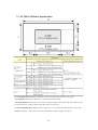
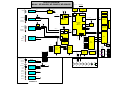
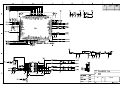
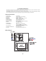
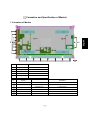
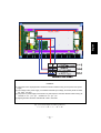
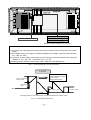
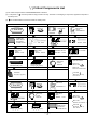
BLOCK DIAGRAM
Model : NP-42H4B9, NP-50H4D9, NP-60H4G9
RXD_u
TXD_u
YC_out2
EEPROM
1K Byte
DVI-D Input
DVI Input
Audio_DVI
Address Driver
Scan Driver
Display
Timing
Generator
&
Display
Port
CTRL Board
V33S
A5V
A5V
Pixelworks
Scaler
PW218-10
V33PW33
74ACT08A
RGB
V18PW33
KPD[0:6],LED
HV
RGB Input
UART
Audio RGB_ L
HV
Y
Pr/Cr
Sync
Processing
Output
Formatting
Pixelworks
Video Signal
Processor
PW3300-10L
RGB
Input Port1
Sync
Decoder
Auto
Image
Optimizer
Vs ON
Video
Decoder(2D,3D)
Audio C_ L
YC_out1
YC_out2
Audio_C1
A9V
SV1
SC1[V,L,R]
V1
Video BNC_ In
MM1031XM
S-Video Input
Video Input
SV1
Audio L
L1,R1
Audio R
Video2_ In
Audio 2_ L
SC2[V,L,R]
Video 2
Audio 2_ R
Video1_ In
Audio 1_ L
Video 1
SC1[V,L,R]
Audio 1_ R
Sub Board
A5V
Audio_RGB
External
Speaker
Output
(Option)
R
Internal
Speaker
Output
5VS
Micronas
Sound
Processor
MSP4450K
R
Rext
Rmain
Lmain
Lext
Phone JACK
Rint
Menu
L
Lint
ADD12V
V33S
V33S
- VOL +
Rext
Rint
Lint
IRRCVR0
KPD[0:6], LED
Tripath
Audio AMP
TA2024B
IRRCVR0
KPD[0:6], LED
A5V, V8AUD
A9V
5VS
FAN(60" Only)
V1.8PW33
Input
V_out1
24V
V1.8PW23
5VS
SC1[V,L,R]
SC2[V,L,R]
SC1[V,L,R]
SC2[V,L,R]
L1,R1
SV1
SV1
V1
L1,R1
V1
S-Video_In
24V
V33PW33
L1,R1
5VS
Audio Out L
Audio Out R
V_out1
Monitor
Output
9Vsc
5Vsc
Power
Regulator
V33PW23
SC2[V,L,R]
Monitor BNC_ Out
9Vsc
5Vsc
V33S
SDRAM
HY57V161610ETP-6
16Mbit
Audio_DVI
Toshiba
A/V Switch IC
TA8851
5Vst_by
V25S
LR_out2
L1,R1
5Vst_by
SMPS
V18S
LR_out1
V1
RLY ON
ADD12V
MBD[00:15],
MBA[00:10]
Audio C_ R
Vs ON
RLY ON
ADC
Audio_C1
TXD_u
IR
Decoders
YPbPr1
YPbPr1
Componet
Input
IN1R[2:9]
IN1G[0:9]
IN1R[0:9]
V18S, V25S, V33S
AudioRGB_ R
110Msps
TMDS&HDCP1.0
IRRCVR0
TMDS_DVI
Color Plasma
Display Panel
RXD_u
Audio_RGB
Pb/Cb
EEPROM
32K Byte
GPIO
Common Sustain Driver
EEPROM
1K Byte
RGB Input
LVDS
Channel1
LVDS Channel1
Audio DVI_ L
Audio DVI_R
PDP Module
MA(12:0),
MD(31:0),
MDQS(3:0)
Input Port0
Sync
Decoder
Auto
Image
Optimizer
Pixelworks
Video Signal
Processor
PW2250-10L
TMDS_DVI
Main Board
Frame Buffer Memory
Controller DDR
SDRAM
ROM
Interface
IN0R[2:9]
IN0G[0:9]
IN0R[0:9]
Output
Formatting
ADC
DDR SDRAM
HY50U573222-FP33
256Mbit
A[01:20],
D[00:15]
V18PW23
V33PW23
MAX232
Transmitter
/Receiver
2006.09.18
Flash ROM
A29L800ATV-70F
8M Bit
5VS
RS-232C
RXD
TXD
A5V
RS-232C
Revision 0.1
Control Board
LED
IR
L
Lext
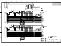
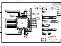
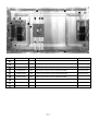
NP-42S4-Main-04(06.04.04).sch-1 - Thu Oct 12 16:22:02 2006
NP-42S4-Main-04(06.04.04).sch-2 - Thu Oct 12 16:22:02 2006
NP-42S4-Main-04(06.04.04).sch-3 - Thu Oct 12 16:22:07 2006
NP-42S4-Main-04(06.04.04).sch-4 - Thu Oct 12 16:22:13 2006
NP-42S4-Main-04(06.04.04).sch-5 - Thu Oct 12 16:22:17 2006
NP-42S4-Main-04(06.04.04).sch-6 - Thu Oct 12 16:22:27 2006
NP-42S4-Main-04(06.04.04).sch-7 - Thu Oct 12 16:22:52 2006
NP-42S4-Main-04(06.04.04).sch-8 - Thu Oct 12 16:22:55 2006
NP-42S4-Main-04(06.04.04).sch-9 - Thu Oct 12 16:23:07 2006
NP-42S4-Main-04(06.04.04).sch-10 - Thu Oct 12 16:23:09 2006
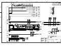
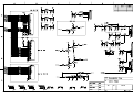
NP-42S4-SUB BNC-04(20060706).sch-1 - Thu Oct 12 16:34:29 2006
NP-42S4-SUB BNC-04(20060706).sch-2 - Thu Oct 12 16:34:29 2006
NP-42S4-Control-03.sch-2 - Sat Aug 05 14:50:54 2006
NP-42S4-Control-03.sch-1 - Sat Aug 05 14:50:53 2006
NP-60H4-Control_Key-01.sch-2 - Wed Oct 18 16:56:14 2006
NP-60H4-Control_Key-01.sch-1 - Wed Oct 18 16:56:13 2006
NP-60H4-Control_IR-01.sch-2 - Wed Oct 18 16:52:43 2006
NP-60H4-Control_IR-01.sch-1 - Wed Oct 18 16:52:42 2006
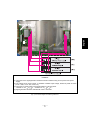
Image Board Inspection Methods
Revision 1.0
1. Application Limits
This instruction is applied to the inspection of PDP Products.
2. Application Model: PMCP642(NP-42H4), PMCP650(NP-50H4), PMCP660(NP-60H4)
3. The General
3.1 This test of Inspection is applied to set which is adjusted accurately according to the
Inspection of PMCP642(NP-42H4), PMCP650(NP-50H4), PMCP660(NP-60H4)
3.2 This test of Inspection can be modified according to transition of production Team and R&D
department.
4. The Conditional :
This inspection is tested in 20℃ standard temperature, 65% standard humidity.
5. The additional :
This inspection can be tested in normal temperature and normal humidity.(15~35℃, 45~85%)
The Registered date
(
• No distributing
Distributor
Whole words
• Cover distributor
WoosungNextier Corp.
-1WoosungNextier Corp.
)team Opinion
-2WoosungNextier Corp.
TABLE OF CONTENTS
1. General Specification
1) In/Out Terminals Spec.
2) Speaker Output Spec.
2. Inspection of Standardization
1) Pattern
2) Speaker Output
3) Input/Output
3. Inspection of the function of electric circuit
1) LED On/Off Test
2) KEY PAD / REMOTE CONTROLER Test
3) VIDEO 1,2 Input
4) VIDEO Input
5) Monitor Output
6) S-VIDEO Input
7) COMPONENT Input
8) RGB Input
9) DVI Input
10) RS232C Control TEST
11) Image Menu
12) Screen Menu
13) Setup Menu
14) Sound Menu
15) Remote controller Function Key Test :
Mute, Locate, SIZE, SWAP(Swap), A.SWAP(Audio Swap),
Split Screen, S.SELECT, Input (Input choice),
Auto(Auto default), I.SIZE(choice of screen size),
FREEZE(Screen), Recall(Input),Sleep(Reservation of Sleep)
4. Out Going Specification
1) Menu Mode Selection.
1. General Specification
-3WoosungNextier Corp.
1) In/Out Terminals Spec.
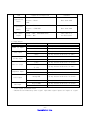
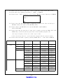
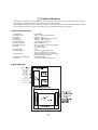
NO.
1
2
ITEM
RS-232C
DVI
D-Sub 9-pin x 1
TXD/RXD(1:1)
DVI Jack x 1
Digital RGB : TMDS
(24 Pin)
MAX : 720p, 1080i, 1280 x 1024 / 60 Hz (SXGA)
RCA Jack(L+R) x 1
Audio : 0.5V[rms](Normal)/2 Channel (L+R)
Input
3
Analog RGB : 0.7V[p-p](75Ω), H/CS/V:TTL(2.2 kΩ),
RGB
Input
D-Sub Jack x 1
(15 Pin)
RCA Jack(L+R) x 1
4
Audio : 0.5V[rms](Normal)/2 Channel (L+R)
S-Video Input
RCA Jack(L+R) x 1
Audio : 0.5V[rms](Normal)/2 Channel (L+R)
BNC Jack x 1
Video : 1V[p-p] (75 Ω)
RCA Jack(L+R) x 1
Audio : 0.5V[rms](Normal)/2 Channel (L+R)
Mini DIN Jack x 1
Y: 1V[p-p] (75 Ω), C: 0.286V[p-p] (75 Ω)[NTSC]
(4 pin)
Y: 1V[p-p] (75 Ω), C: 0.300V[p-p] (75 Ω)[PAL/SECAM]
BNC Jack x 1
Video : 1V[p-p] (75 Ω)[NTSC/PAL/SECAM]
RCA Jack(L+R) x 1
Audio : 0.5V[rms](Normal)/2 Channel (L+R)
RCA Jack x 1
Video : 1V[p-p] (75 Ω)[NTSC/PAL/SECAM]
Video Input
VIDEO 1 Input
Pr/Cr:0.7V[p-p](75Ω)
EDTV : 480i, 576i, 576p, 480p, 720p, 1080i
Monitor Output
7
8
MAX : 720p, 1080i, 1280 x 1024 / 60 Hz (SXGA)
Pb/Cb:0.7V[p-p](75Ω),
RCA Jack x 1
Input
6
SOG:1V[p-p](75Ω)
Y:1V[p-p](75Ω)
Component
5
SPECIFICATION
Audio : 0.5V[rms](Normal)/2 Channel (L+R)
9
VIDEO 2 Input
RCA Jack x 1
Video : 1V[p-p] (75 Ω)[NTSC/PAL/SECAM]
Audio : 0.5V[rms](Normal)/2 Channel (L+R)
2) Speaker Output Spec.
-4WoosungNextier Corp.
(1)Internal speaker
NO.
ITEM
SPECIFICATION
UNIT
REMARK
1
Freq. Response
0.17 ~ 20
KHz
2
T.H.D
Max. : 5
%
400Hz 10W
3
Output
10 + 10
W
RMS
4
Impedance
8 + 8
Ω
5
Output sound pressure
88
Speaker Output
dB/W/M
2. Inspection of Standardization
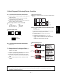
1) TEST PATTERN
(1) MONO SCOPE
Item
Resolution
Condition
Standard Value
MONOSCOPE
More than 400 (H)
Standard Mode
OVER SHOOT
Same as above
Can be recognized
PRE SHOOT
″
″
Frequency Sync. Range
MONOSCOPE
MONOSCOPE
OVER SCAN
Horizontal
±120lines ~ ±480lines
Vertical
- 15lines - 9lines
Horizontal
Less than +10%
Vertical
Less than +10%
The half of
Bright.
Contrast Max.
ON SCREEN Remarking
Position
MONOSCOPE
Vertical CENTER
RETMA PATTERN
Adjustment
(Clear Screen)
Horizontal CENTER
Adjustment
Same as above
Should not be cut in a picture
The central cross line of RETMA PATTERN PDP
Should match the Panel of mechanical CENTER
Vertical CENTER ±5mm
The Central vertical line of RETMA PATTER
Should balance in left/right. CENTER ±10mm
-5WoosungNextier Corp.
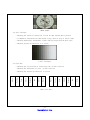
<MONO SCOPE>
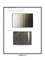
(2) Stair 10-Steps
- Checking the extent of saturation of left & right black & white pattern
- It Should be saturated less than black 2 step, white 2 step in left & right
- Checking unnecessary chrominance signal came up except black & white sync.
- Checking distortion and noise in a screen
< Stair 10-Steps>
(3) Color Bar
- Checking the reiterations of contacting side in each color bar
- Checking the difference of color in each color bar
<PAL, PAL-M, PAL-N>
<NTSC,NTSC-4.43MHz>
<Full Color Bar>
-6WoosungNextier Corp.
blue
Red
Magenta
Green
Cyan
Yellow
White
Black
Green
Red
Magenta
Green
Cyan
Yellow
White
- Checking the distortion and noise in screen
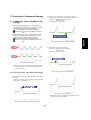
(4) Multi Burst
- Checking the range of Frequency Response
- Checking the distortion and noise in screen
< Multi burst>
Color System
Multi-Burst
NTSC, NTSC-4.43MHz
PAL, PAL-M, PAL-N, SECAM
0.5-1.0-2.0-3.0-3.58-4.2MHz
0.5-1.0-2.0-3.0-4.0-4.8MHz
Within 1.0dB
Within 1.0dB
Frequency
Frequency
characteristic
Setup
0%
7.5%NTSC only
0%
White REF Signal
714.3mV
714.3mV
700.0mV
Multi-Burst
357.2mV
384.0mV
385.0mV
0mV
53.6mV
0mV
pedestal
Black level
-7WoosungNextier Corp.
(5) Cross Pattern
- Checking something dropped out of horizontal, vertical line
- Checking the same interval between Crosshatch
- Checking the distortion and Noise
< Cross Pattern 16:9>
Aspect ratio
4:3
16:9
White Level 0%setup
525
625
525
625
White Level 0%setup
714.3mV
700.0mV
714.3mV
700.0mV
NTSC only
714.3mV
Black Level 0%setup
0 mV
Black Level 0%setup NTSC only
53.6 mV
Line
system
714.3mV
0 mV
0 mV
0 mV
53.6mV
NO. of horizontal crosshatch
17
23
No. of vertical crosshatch
13
13
296ns±100ns
296ns±100ns
2 lines
2 lines
2.96us±0.3us
2.22us±0.3us
525system
36 lines
36 lines
625system
44 lines
44 lines
Pulse width
Horizontal
Vertical
Crosshatch width
Horizontal
Vertical
-8WoosungNextier Corp.
(6) 64-gradation block gray
- Checking the saturation of between splinter
- Seeing the difference of Brightness/Contrast
- Checking the distortion and noise in screen
<64-Gradation Block Gray>
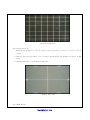
(7) Crosshatch & circle & gray
<Crosshatch & Circle & Gray>
-9WoosungNextier Corp.
- Checking that it is something dropped out of in horizontal, vertical line of
crosshatch
- Checking that the interval between crosshatch line is equal
- Checking that printing-out of exact circle shape is right
- Checking brightness, contrast through gray pattern
- Checking that the distortion and noise is in screen
(8) Crosstalk
- Checking that Burst line is clear
- Checking that there is no distortion and noise
< Crosstalk>
(9) 8-black Crosshatch
- Checking that it is something dropped out of in horizontal, vertical line of
crosshatch
- Checking that the interval between line is equal
- Checking that there is no distortion and noise
-10WoosungNextier Corp.
<8-black Crosshatch>
(10) Display Position
- Checking the balance of left & right & top & bottom in a base of vertical line of
center.
- Checking that the horizontal line of center should match the mechanical center of PDP
Panel.
- Checking that there is no distortion and noise
< Display position>
(11) SMPTE RP-133
-11WoosungNextier Corp.
- Checking that it is something dropped out of in horizontal, vertical line of
crosshatch
- Checking that there is no problem of handling high frequency Sync.
- Checking Multi-bust Signal Frequency
- Checking that there is no distortion and noise
]
< SMPTE RP-133>
(12) 256Gray+RGBW Color Bar
- Checking the reiterations of contacting side In each color bar
- Checking that the printing-out of color is right
- Checking the range if Saturation
- Checking that there is no distortion and noise
<256gray+RGBW color bar>
※(1)~(5) Pattern is the standard of ShibaSoku (TG-19CC) Signal
and (1) ~(5) Pattern is applied to VIDEO, S-VIDEO and VIDEO1,2 Input.
※(6)~(12) Pattern is the standard of ASTRODESIGN(VG-848) Signal
and (6) ~ (12) Pattern is applied to RGB, DVI, Component Input.
2) Speaker Output
-12WoosungNextier Corp.
Item
Signal/Noise
Ratio
Signal/Buzz
Ratio
Max. Audio
output
Condition of Inspection
Standard
Sound : 1KHz, more than 30% MODULATION
Picture : Black
More than 37dB
50mW
Sound : 1KHz, more than 30% MODULATION
Picture : COLOR BAR
More than 35dB
50mW
Sound : 1KHz, 100% MODULATION
More than 9 W
Volume : Max.
8Ω Resistance
3) Input/Output
Input
VIDEO 1,2 Input
Video Input
S-Video Input
Monitor Output
Condition
Video
No any distortion & noise in Screen
Audio
No any distortion & noise in Audio
Video
No any distortion & noise in Screen
Audio
No any distortion & noise in Audio
Y,C
No any distortion & noise in Screen
Audio
No any distortion & noise in Audio
Video
No any distortion & noise in Screen
Audio
(L + R)
Component Input
R,G,B Input
DVI Input
standard
No any distortion & noise in Audio
Y, Pb(Cb), Pr(Cr)
No any distortion & noise in Screen
Audio
No any distortion & noise in Audio
Analog RGB
No any distortion & noise in Screen
Audio
No any distortion & noise in Audio
Digital RGB
No any distortion & noise in Screen
Audio
No any distortion & noise in Audio
※ Video Signal Cross-Talk Level
- Should not be hindered by other signal input when signal inputs all inputs of signal
-13WoosungNextier Corp.
3. Test of function of electric circuit
1) LED 0n/Off Test
(1) Checking that the stand-by signal –red- is lighting on
(2) Checking that working condition(power on) –green- is lighting on
(3) Checking that no signal condition LED is blinking
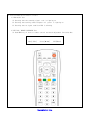
2) KEY PAD / REMOTE CONTROLER Test
(1) Push MENU key of front or remote control and check adjustment like below Box.
MENU
Move[-VOL+]
Select[▼ ▲]
-14WoosungNextier Corp.
EXIT[Menu]
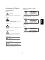
3) VIDEO 1,2 Input
(1) Please connect the signal of VIDEO Input to VIDEO Input as RCA Cable
(2) Please power on by pushing [POWER]key of front or remote controller
(3) Please select VEDEO Input by using [-VOL+] and [▼ ▲]key after pushing [INPUT]key
INPUT
VIDEO1
VIDEO2
.
(4) Press the TEXT button
(The Closed Caption Menu is displayed)
(5) Press the TEXT button to select option
(OFF,CC1,CC2,CC3,CC4,TEXT1,TEXT2,TEXT3,TEXT4)
(6) Please check CC1 is working well, connecting Closed Caption signal of ShibaSoku(TG19CC) or VCR(SV-7000W) : This function works only in ‘Normal split mode’
(7) Please check that the video signal in each mode is working well
(8) Please check that Sound is working well by pushing [-VOL+]key of front or remote
controller
4) VIDEO Input
(1) Please connect the signal of VIDEO Input to VIDEO Input as BNC Cable
(2) Please power on by pushing [POWER]key of front or remote controller
(3) Please select VEDEO Input by using [-VOL+] and [▼ ▲]key after pushing [INPUT]key
INPUT
VIDEO1
VIDEO2
VIDEO
.
(4) Press the TEXT button
(The Closed Caption Menu is displayed)
(5) Press the TEXT button to select option
(OFF,CC1,CC2,CC3,CC4,TEXT1,TEXT2,TEXT3,TEXT4)
(6) Please check CC1 is working well, connecting Closed Caption signal of ShibaSoku(TG19CC)or VCR(SV-7000W) : This function works only in ‘Normal split mode’
-15WoosungNextier Corp.
(7) Please check that the video signal in each mode is working well
(8) Please check that Sound is working well by pushing [-VOL+]key of front or remote
controller
5) Monitor Output
(1) Please connect VIDEO Input signal to VIDEO Input as BNC Cable
(2) Please connect the output of test installation to Monitor output as BNC Cable
(3) After connecting 8 Ω dummy resistance to speaker output in left, right please connect
Multi-Meter to in each edge of dummy resistance
(4) Please power on by pushing [POWER]key of front or remote controller
(5) Please select VIDEO through [-VOL+] and [▼ ▲]key after pushing [INPUT]key
INPUT
VIDEO1
VIDEO2
VIDEO
.
(6) Please check that All in-coming video signal is working well
(7) Please check that Video signal is appearing in Monitor Output
(8) Please adjust Audio sound with max through [–VOL+]key of owner’s remote controller
(9) Please check that the maximum of incoming Audio signal is more than 8.8V[rms]
(10) Please check 8 Ω in left & right of speaker output and Multi-Meter
(11) Please check that audio sound is good by pushing [-VOL+]key
(12) Please check that Video signal(V) and Audio signal(R+L) is having right output
(13) Please power OFF by pushing [POWER]key of front or remote controller
(14) Please check that Video signal(V) and Audio signal(R+L) is having right output
6) S-VIDEO Input
(1) Please connect S-VIDEO terminal as S-Video Cable to S-VIDEO output
(2) Please connect Audio input terminal as RCA Audio Cable to Audio output
(3) Please power on by pushing [POWER]key of front or remote controller
(4) Please select S-VIDEO by pushing [-VOL+] and [▼ ▲]key after [INPUT]key
INPUT
.
S-VIDEO
.
-16WoosungNextier Corp.
(5) Press the TEXT button
(The Closed Caption Menu is displayed)
(6) Press the TEXT button to select option
(OFF, CC1,CC2,CC3,CC4,TEXT1,TEXT2,TEXT3,TEXT4)
(7) Please check CC1 is working well, connecting Closed Caption signal of ShibaSoku(TG19CC)
or VCR(SV-7000W) : This function works only in ‘Normal split mode’
(8) Please check all video signal in each mode is having good input in screen
(9) Please check the sound is voiced well by pushing [-VOL+]key
7) COMPONENT Input
(1) Please connect Video & Audio signal to COMPONENT terminal as COMPONENT Cable
(2) Please power on by pushing [POWER]key of front or remote controller
(3) Please select COMPONENT by using [-VOL+] and [▼ ▲]key after [INPUT]key
INPUT
.
COMPONENT
.
(4) Please check video signal is appearing in screen well
(5) Please check that Audio sound is coming out well by pushing [-VOL+]key
(Please check signal of Component Mode Table)
Mode
Resolution
Horizontal
Vertical
Pixel Clock
Frequency (kHz)
Frequency (Hz)
Frequency (MHz)
Remark
EDTV
480i
720 x 480
15.730
29.970
13.5000
Support
EDTV
576i
720 x 576
15.630
25.000
13.5000
Support
SDTV
480p
720 x 480
31.470
59.940
27.000
Support
SDTV
576p
720 x 576
31.250
50.000
27.000
Support
1280 x 720
45.000
60.000
74.250
Support
44.960
59.940
74.180
Support
37.500
50.000
74.250
Support
33.750
30.000
74.250
Support
33.720
29.970
74.180
Support
31.250
25.000
74.250
Support
28.125
25.000
74.250
Support
HDTV
HDTV
720p
1080i
1920 x 1080
<Component Mode Table >
-17WoosungNextier Corp.
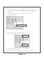
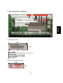
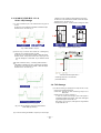
8) RGB Input(DDC DATA WRITE is optional per Buyer)
(1) Please connect the Parallel Port of DDC WRITER and the Parallel Port of PC to Cable.
(2) Please connect the ANALOG Port of DDC WRITER and the RGB Port of MAIN BOARD
to RGB Cable.
(3) Please send for RGB DDC FILE by pushing LOAD FILE after excelling the
DDC WRITE PROGRAM of PC.
DDC DATA File Load
(4) Write Please choose Write Port(DSUB 15(Analog))
(5) Please change DDC DATA to Write format by pushing "Write" button.
WRITE PORT
White Button
(6) Please check DDC DATA by reading.
(7) Connect the out-coming of RGB Video signal to RGB input as 15 Pin D-Sub
-18WoosungNextier Corp.
(8) Connect the out-coming of RGB Audio signal to RGB Audio input as RCA Audio Cable
(9) Please power on by pushing front KEY or “POWER” of REMOCON
(10) Please select “RGB”terminal by using [-VOL+],[▼ ▲]key after Input key of REMOCON
INPUT
VIDEO 1
.
RGB
(11) Please check that RGB Video signal is appearing in screen well after switching to
RGB Mode (Check the signal of DVI/RGB Mode Table)
(12) Please connect the RGB PORT of PC and the RGB PORT of MAIN BOARD to
15Pin D-SUB CABLE.
(13) Please check that the function of frame lock is normal by using the SCROLL KEY in KEY
BOARD and by controlling moving speed after excelling BLIT program of PC.
(The range of Frequency o Frame lock is 57Hz < Vsync < 61Hz)
* Frame lock working condition : Screen should not disappear when the screen be movable.
(14) Please check the Sound is good by pushing CONTROL KEY or “-VOL+”KEY of REMOCON
Mode
VGA
SVGA
Resolution
Remark
Horizontal
Vertical
Pixel Clock
Frequency (kHz)
Frequency (Hz)
Frequency (MHz)
640 x 350
31.460
70.000
25.170
Support
640 x 400
37.861
85.000
31.500
Support
720 x 400
31.469
70.000
28.320
Support
640 x 480
31.460
50.000
25.170
Support
31.500
60.000
25.175
Support
37.700
72.000
31.500
Support
37.500
75.000
31.500
Support
43.300
85.000
36.000
Support
35.100
56.000
36.000
Support
37.900
60.000
40.000
Support
48.100
72.000
50.000
Support
46.900
75.000
49.500
Support
53.700
85.000
56.250
Support
49.720
75.000
57.280
Support
800 x 600
832 x 624
< DVI/RGB Mode Table(1/2) >
-19WoosungNextier Corp.
Mode
Resolution
Remark
Horizontal
Vertical
Pixel Clock
Frequency (kHz)
Frequency (Hz)
Frequency (MHz)
48.400
60.000
65.000
Support
56.500
70.000
75.000
Support
60.000
75.000
78.750
Support
64.000
80.000
85.500
Support
68.300
85.000
94.500
Support
870
68.680
75.000
100.000
Support
SXGA
1280 x 1024
64.000
60.000
108.000
Support
WXGA
1366 x 768
60.000
84.400
Support
SDTV 480p
720 x 480
31.470
59.940
27.000
Support
SDTV 575p
720 x 576
31.250
50.000
27.000
Support
HDTV
1280 x 720
45.000
60.000
74.250
Support
44.960
59.940
74.180
Support
37.500
50.000
74.250
Support
33.750
30.000
74.250
Support
33.720
29.970
74.180
Support
31.250
25.000
74.250
Support
28.125
25.000
74.250
Support
XGA
1024 x 768
1152 x
HDTV
720p
1080i
1920 x 1080
50.000
< DVI/RGB Mode Table(2/2) >
-20WoosungNextier Corp.
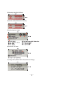
9) DVI Input
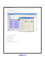
(1) Please connect the Parallel Port of DDC WRITER and the Parallel Port of PC to Cable.
(2) Please connect the DVI Port1 of DDC WRITER and the DVI Port of MAIN BOARD to DVI
Cable.
(3) Please send for DVI DDC FILE by pushing LOAD FILE after excelling
the DDC WRITE PROGRAM of PC.
DDC DATA File Load
(4) Please choose Write Port(DVI(Digital)) or DVI2(Digital))
(5) Please change DDC DATA to Write format by pushing "Write" button.
WRITE PORT
White Button
(6) Please check DDC DATA by reading.
(7) Connect ASTRO VG-848H of DVI output to DVI Video input
(8) Connect Audio out- coming of ASTRO VG-848H of DVI to DVI audio input
(9) Please power on PDP TV by pushing front key or “POWER” KEY of REMOCON
-21WoosungNextier Corp.
(10)Please select DVI Input by using [-VOL+], [▼ ▲ ]key after pushing front KEY or
INPUT of REMOCON
INPUT
.
RGB
DVI
(11) Check DVI video signal is appearing well in screen after moving to DVI Input
(Check the signal of DVI/RGB Mode Table)
(12) Please connect the DVI PORT of PC and the DVI PORT of MAIN BOARD to DVI CABLE.
(13) Please check that the function of frame lock is normal by using the SCROLL KEY in KEY
BOARD and by controlling moving speed after excelling BLIT program of PC.
(The range of Frequency o Frame lock is 57Hz < Vsync < 61Hz)
* Frame lock working condition : Screen should not disappear when the screen be movable.
(14) Check the sound is good after pushing the front key or “-VOL+”KEY of REMOCON
(15) Please connect the Serial Port of PC and the RS232C Port of Main Board to 9 Pin D-SUB
Cable
(16) Please execute the PWKeyLoader program
(17) Please click Setup tap and check the configuration of PWKeyLoader
(18) Please click Load. Then the HDCP key would be written
(19) Please connect the DVI output(with HDCP) of DVD Player and DVI input of Main Board
to DVI Cable
(20) Please check that video signal of HDCP is appearing rightly in screen
(21) Please check that Sound is good by pushing [-VOL+]key of front or remote control
-22WoosungNextier Corp.
10)RS232C Control TEST
(1) Please connect the Serial Port of PC and the RS232C Port of Main Board
to 9 Pin D-SUB Cable
(2) Please execute the Docklight.exe
(3) Please choose Hardware Protocol as below.
- Baud rate : 19,200 bps
- Data bits : 8 bit
- Parity bits : NONE
- Stop bits : 1 bit
- Parity Error Character : Don’t care
-23WoosungNextier Corp.
(4) Please check that RS232C CONTROL works well by putting the HEX MODE in program of
Serial Test through referring to Serial Control Protocols Manual.
ex) MUTE ON/OFF TEST (PDP ID : 01)
Mute : m (0x6d)
▶ To Control Mute On/Off
(1) Transmission
[0x57][m][ ][Display ID][ ][Data][CR][LF]
Data = 0(00h) : Off
-----Æ57 6D 20 01 20 00 0D 0A
Data = 1(01h) : On
-----Æ57 6D 20 01 20 01 0D 0A
(2) OK Ack
[0x06]
(3) Error Ack
[0x15]
▶ Read Mute Status
(1) Transmission
[0x57][m][ ][PDP ID][ ][0xFF][CR]
-----Æ57 6D 20 01 20 FF 0D 0A
(2) OK Ack
[Data]
Data = 0(00h) : Off Status
Data = 1(01h) : On Status
(3) Error Ack
[0x15]
(5) Please check Command for [Operation Time] and [Reversal Image]
(Working at only RS232C CONTROL mode)
- [Operation Time] : Check operation time of PDP
- [Reversal Image] – ON : Check image is reversed
- OFF : Check image is defaulted
-24WoosungNextier Corp.
11) Image Menu
(1) Please enter into Image MENU by pushing front key or MENU of REMOCON
Image
Brightness
Contrast
Sharpness
Color
Tint
Video Defaults
(2) Checking that adjustment can be possible for whatever user want to adjust by pushing
front key or [▼ ▲],[-VOL+]KEY of REMOCON
- Brightness : Resolution
- Contrast : Contrast
- Sharpness : Clearance
- Color : the tone of color
- Tint : the depth of color
- Video Defaults: Image Mode first default
12) Screen
(1) enter into Screen MENU by pushing front key or MENU of REMOCON
Screen
Size
Freeze
Pixel Shift
(2) Please check following function can be working after selecting what function you want
by
Pushing front KEY or [- VOL +],[▼ ▲]key of REMOCON
- Size : AUTO,FILL ALL, FILL ASPECT, ZOOM, ANAMORPHIC, WIDE,
- Freeze: Screen still
- Pixel Shift : Panel Burn-in Protection
(When it is on the working Sticking Minimum function prevents Panel Burn-in
by moving screen as the left, the right or Up and down in a interval.)
-25WoosungNextier Corp.
13) Setup Menu
(1) Please enter into Image MENU by pushing front key or MENU of REMOCON
Setup
Language
Sleep Timer
OSD Setting
Menu Transparency
Menu Timeout
Color Temp.
(2) Check that adjustment can be possible for whatever user want to adjust by pushing
[▼ ▲] and [-VOL+]key
- Language : Each country language (This is optional by buyer)
- Sleep Timer : Reservation of sleep time
- OSD Setting
* Menu Transparency : OSD the degree of clearness adjustment
* Menu Timeout : OSD Time adjustment
- Color Temp. : Choice color temperature(WARM/NORMAL/COOL)
14) Sound Menu
(1) Please check the volume of sound is adjustable by pushing front key or “-VOL+”KEY
of REMOCON
(2) Please enter into Sound MENU by pushing front KEY or MENU KEY of REMOCON
Sound
Volume
Treble
Bass
Balance
Mute
Audio Defaults
(3) Checking that adjustment can be possible for whatever user want to adjust by
pushing front key or [▼ ▲],[-VOL+]KEY of REMOCON
-26WoosungNextier Corp.
- Treble : High sound of Volume
- Bass : Low sound of Volume
- Balance : Sound balance
- Mute : Quiet
- Audio Defaults: returning to Audio first Mode
15) Remote controller Function Key Test
(1) Checking following details by pushing function key of REMOCON
- Mute(Quietly) : Once pushed at one time sound is dead. Once pushed again return to
the originated mode.
- Input : It help you see the input mode
-
Auto(Auto
setting)
:
It
can
help
H.V
position/Phase/Frequency
searching
automatically in RGB Input
- I.SIZE(Screen size) : It can help screen size change like AUTO,FILL ALL, FILL
ASPECT, ZOOM, ANAMORPHIC, WIDE
- FREEZE(Screen freeze) : Once a time screen is freezed and Once pushed again it
return to default
- Recall(Input expression) : It help viewing in present input signal
- Sleep(sleep timer) : It can reserve the sleeper time whenever you push button
( OFF -> 30Minute -> 60Minute -> 90 Minute -> 120 Minute -> 150 Minute -> 180 Minute)
-
Split Screen : Picture is changed like below when user push Split key of Remocon
Main
PIP
PBP
< Normal -> PIP -> PBP >
-27WoosungNextier Corp.
■ PIP Settings
Sub Input
VIDEO 1
VIDEO 1
VIDEO
S-VIDEO
VIDEO 1
X
O
O
O
VIDEO 2
O
X
O
O
VIDEO
O
O
X
O
S-VIDEO
O
O
O
X
COMPONENT ◆
O
O
O
O
RGB ◆
O
O
O
O
DVI ◆
O
O
O
O
Main Input
“◆”Max : 480p, 576p,1366 X 768/60Hz
In the PIP mode, the sub input source is differently defined for
the default value(video1 or video2) depending on your PDP model
- Locate(Screen Position) : Please move PIP Position from PIP Mode
- SIZE : PIP SCREEN Size is changing in PIP Mode
- SWAP(Swap) : This function has main screen switch off sub screen
- A.SWAP(Audio Swap) : This function has sound of main screen switch off sub screen
- S.SELECT : This function help selecting the each screen from Split Screen
-28WoosungNextier Corp.
4. Out Going Specification
1) Menu Mode설정.
(1) Video1/2, Video, S-Video and Component Input
NO.
Menu
Function
Default
1
Image
Brightness
050
Contrast
050
Sharpness
002
Color
050
Tint
050
Video Defaults
[-VOL+] TO Restore Defaults
Size
AUTO
Freeze
OFF
Pixel Shift
OFF
Language
English
Sleep Timer
000
2
3
Screen
Setup
REMARK
OSD Setting
4
Audio
Menu Transparency
000
Menu Timeout
020
Color Temp.
NORMAL
Volume
30
Treble
050
Bass
050
Balance
050
Mute
OFF
Audio Defaults
[-VOL+] TO Restore Defaults
<
Table 1
>
※ Image, Screen, Setup, Audio Menu is the same as < Table 1>
-29WoosungNextier Corp.
(2) RGB Input
NO.
Menu
Function
Default
1
Image
Brightness
050
Contrast
050
REMARK
Phase
Frequency
2
Screen
Sharpness
002
Video Defaults
[-VOL+] TO Restore Defaults
Size
AUTO
H Position
V Position
Auto Positioning
3
Setup
Freeze
OFF
Pixel Shift
OFF
Language
English
Sleep Timer
000
OSD Setting
4
Audio
Menu Transparency
000
Menu Timeout
020
Color Temp.
NORMAL
Volume
30
Treble
050
Bass
050
Balance
050
Mute
OFF
Audio Defaults
[-VOL+] TO Restore Defaults
<
Table 2
>
-30WoosungNextier Corp.
(3) DVI Input
NO.
Menu
Function
Default
1
Image
Brightness
050
Contrast
050
Sharpness
002
Video Defaults
[-VOL+] TO Restore Defaults
Size
AUTO
Freeze
OFF
Pixel Shift
OFF
Language
English
Sleep Timer
000
2
3
Screen
Setup
REMARK
OSD Setting
4
Audio
Menu Transparency
000
Menu Timeout
020
Color Temp.
NORMAL
Volume
30
Treble
050
Bass
050
Balance
050
Mute
OFF
Audio Defaults
[-VOL+] TO Restore Defaults
<
Table 3
>
-31WoosungNextier Corp.
9-BNC Firmware Upgrade Manual
Revision 0.1
(1) Connect PC and PDP with RS-232C Cable (1:1 Serial cable).
(2) Remove AC Power Cord from PDP for Power off.
(2) Run "C:\......\FlashUpgrader.exe".
(3) Click "Flash" button.
(4) Connect AC Power Cord of PDP.
(5) Right after connecting AC Power Cord, automatically up-grading.
(6)
After finishing Up-grade, click " Close " button to end program.
(7)
Remove RS-232C Cable ( 1:1 Serial Cable).
(8)
Remove and reconnect AC Power Cord of PDP.
(9)
Turn on PDP and Check the Panel Selection.(Default : 42” SD)
(10) If Panel Selection not corrected, Change the Panel selection.
(11) Value of Panel Selection can be changed as like below through.
Pushing [VOL+], [▼] and [▲] then [Panel Select] OSD is shown.
(12) Push [VOL-] or [VOL+] button to select panel.
000 : 42”SD(Default) panel is selected.
001 : 42”HD panel is selected.
002 : 50”HD or 60”HD panel is selected.
003 : LCD panel is selected.
(13) Pease push power button off and power button on after OSD menu is placed
In the middle of screen by pushing [MENU] button – That means panel choice
Is selected in right
(14) If OSD Menu is not placed in the middle of screen return to No.(11) as
Pushing [VOL+], [▼] and [▲] button at the same time.
(15) Please check the correct panel by viewing OSD Menu after Power On.
- End -
-1Woosung Nextier Corp.
● Purpose
This document describes how to operate the 9-Model Series, using the RS-232 Serial Communication
Interface. This document defines all the command and messages exchanged between the Master (a
PC or the other controller) and the Slave (the displays). It also describes the ways to send or read the
commands or the messages.
● Protocol definition
SICP stands for “Serial Interface Communication Protocol”.
The protocol is specifically designed to allow data communication in half duplex multi-point environments,
but it can also be used for half duplex point-to-point RS-232 communication.
● Communication characteristics
A half duplex communication is implemented starting from the concept of a master-slave structure, where
the display is supposed to be the slave.
The first action is always taken by the master, which can be either a PC or any controlling device (acting
as server) interfaced to the monitor. After sending a command or a request in the appropriate format the
master receives from the slave an acknowledgement, which tells the transmitter whether the command is
not valid (or not executable, anyway) or it is accepted.
In case of a request, the requested information is sent back and it becomes the acknowledgement by
itself.
● How to connect a external equipment
Connect COM Port (9Pin D-Sub Port) of PC and RS-232C of Display with
RS-232C Cable(1:1 Serial cable)
● Hardware Protocol
Baud rate : 19,200 bps
Data bits : 8 bit
Parity bits : NONE
Stop bits : 1 bit
Handshake : NONE
● Transmission Formats
This is the format that the computer will send to the display to execute commands (such as Mute on,
Mute off, etc.). The format for this command transmission is as follows:
[Manufacturer ID ][Command][ ][Display ID][ ][Data][CR][LF]
Name
Manufacturer ID
Command
[]
Display ID
[]
Data
CR
LF
Description
The ID of the Manufacturer
The command to control the Display
Space
The ID of the Display, from [001~254]
Space
The data to be transmitted with the command
Carriage Return
Line Feed
ACSII code
0x57
0x20
0x01~ 0xFE
0x20
0x0D
0x0A
● OK Acknowledgement
The acknowledgement will be sent by the display to the computer to verify that the command has been
successfully received and executed. This format for this acknowledgement is as follows:
[0x06]
● Error Acknowledgement
The Error Values will be sent by the display to the computer to verify that the command has been
successfully received and executed. This format for this Error Values is as follows:
[0x15]
● ASCII code
(American Standard Code for Information Interchange)
*
0
1
2
3
4
5
6
7
8
0 NUL SOH STX ETX EOT ENQ ACK BEL BS
9
A
TAB LF
B
C
D
E
F
VT
FF CR SO SI
1 DLE DC1 DC2 DC3 DC4 NAK SYN ETB CAN EM
SUB ESC FS GS RS US
2
!
"
#
$
%
&
'
(
)
*
+
,
-
.
/
3 0
1
2
3
4
5
6
7
8
9
:
;
<
=
>
?
4 @
A
B
C
D
E
F
G
H
I
J
K
L
M
N
O
5 P
Q
R
S
T
U
V
W
X
Y
Z
[
\
]
^
_
6 `
a
b
c
d
e
f
g
h
i
j
k
l
m
n
o
7 p
q
r
s
t
u
v
w
x
y
z
{
|
}
~
Example 1: ‘A’ character = 4th row, 1st column => Hex : 0x41 , Decimal : 65
● HOW to Choose Display ID number.
The adjustment range of Set ID is 001 ~ 254.
▶ To Choose Display ID number
(1) Transmission
[0x57][?][ ][0x00][ ][Data][CR][LF]
Data = 001(01h)
.
.
Data = 128(80h)
.
.
Data = 254(FEh)
(2) OK Ack
[0x06]
(3) Error Ack
[0x15]
▶ Read Display ID number
(1) Transmission
[0x57][?][ ][0x00][ ][0xFF][CR][LF]
(2) OK Ack
[Data]
Data = 001(01h)
.
.
Data = 128(80h)
.
.
Data = 254(FEh)
(3) Error Ack
[0x15]
● Command List
Name
Command
Data(HEX)
Name
Command
Data(HEX)
1. Mute
3. Remote Control
Lock
5. Keypad Lock
7. Reversal Image
9. Split (PIP/PBP)
m (0x6d)
r (0x72)
00h ~ 01h
00h ~ 01h
2. Power
4. Input (Main)
p (0x70)
i (0x69)
00h ~ 01h
01h ~ 0Eh
k (0x6b)
b (0x62)
s (0x73)
00h ~ 01h
00h ~ 01h
00h ~ 02h
6. Operation Time
8. Volume
10. Input (Sub)
O (0x6f)
v (0x76)
I (0x49)
01h
28h ~ 64h
01h ~ 0Ch
1. Mute : m (0x6d)
2. Power : p (0x70)
▶ To Control Mute On/Off
(1) Transmission
[0x57][m][ ][Display ID][ ][Data][CR][LF]
Data = 0(00h) : Off
Data = 1(01h) : On
(2) OK Ack
[0x06]
(3) Error Ack
[0x15]
▶ Read Mute Status
(1) Transmission
[0x57][m][ ][ Display ID][ ][0xFF][CR][LF]
(2) OK Ack
[Data]
Data = 0(00h) : Off Status
Data = 1(01h) : On Status
(3) Error Ack
[0x15]
▶ To Control Power On/Off of the Display
(1) Transmission
[0x57][p][ ][ Display ID][ ][Data][CR][LF]
Data = 0(00h) : Off
Data = 1(01h) : On (Display ID=[0x00] Fix)
(2) OK Ack
[0x06]:Off , [0xBE..,0xBF..,0xEF..]:On
(3) Error Ack
[0x15]:Off , [X]:On
▶ Read Power Status
(1) Transmission
[0x57][p][ ][ Display ID][ ][0xFF][CR][LF]
(2) OK Ack
[Data]
Data = X(Don’t care) : Off Status
Data = 1(01h)
: On Status
(3) Error Ack
[0x15]
3. Remote Control Lock : r (0x72)
4. Input(Main) : i (0x69)
▶ To Control Remote Control Lock On/Off
(1) Transmission
[0x57][r][ ][ Display ID][ ][Data][CR][LF]
Data = 0(00h) : Off
Data = 1(01h) : On
(2) OK Ack
[0x06]
(3) Error Ack
[0x15]
▶ Read Remote Control Lock Status
(1) Transmission
[0x57][r][ ][ Display ID][ ][0xFF][CR][LF]
(2) OK Ack
[Data]
Data = 0(00h) : Off Status
Data = 1(01h) : On Status
(3) Error Ack
[0x15]
▶ To Select Input(Main) of the Display
(1) Transmission
[0x57][i][ ][ Display ID][ ][Data][CR][LF]
Data = 08(08h) : TV (Option)
Data = 11(0Bh) : SCART 1 or VIDEO 1
Data = 12(0Ch) : SCART 2 or VIDEO 2
Data = 01(01h) : VIDEO
Data = 02(02h) : S-VIDEO
Data = 07(07h) : COMPONENT
Data = 14(0Eh) : RGB
Data = 05(05h) : DVI
Data = 03(03h) : HDMI 1 (Option)
Data = 04(04h) : HDMI 2 (Option)
(2) OK Ack
[0x06]
(3) Error Ack
[0x15]
▶ Read Input(Main) Status
(1) Transmission
[0x57][i][ ][ Display ID][ ][0xFF][CR][LF]
(2) OK Ack
[Data]
Data = 08(08h) : TV (Option)
Status
Data = 11(0Bh) : SCART 1 or VIDEO 1 Status
Data = 12(0Ch) : SCART 2 or VIDEO 2 Status
Data = 01(01h) : VIDEO
Status
Data = 02(02h) : S-VIDEO
Status
Data = 07(07h) : COMPONENT
Status
Data = 14(0Eh) : RGB
Status
Data = 05(05h) : DVI
Status
Data = 03(03h) : HDMI 1 (Option)
Status
Data = 04(04h) : HDMI 2 (Option)
Status
(3) Error Ack
[0x15]
5. Keypad Lock : k (0x6b)
6. Operation Time : o (0x6f)
▶ To Control Keypad Lock On/Off
(1) Transmission
[0x57][k][ ][ Display ID][ ][Data][CR][LF]
Data = 0(00h) : Off
Data = 1(01h) : On
(2) OK Ack
[0x06]
(3) Error Ack
[0x15]
▶ Read Keypad Lock Status
(1) Transmission
[0x57][k][ ][ Display ID][ ][0xFF][CR][LF]
(2) OK Ack
[Data]
Data = 0(00h) : Off Status
Data = 1(01h) : On Status
(3) Error Ack
[0x15]
▶ To Read Operation Time of the Display
(1) Transmission
[0x57][o][ ][ Display ID][ ][Data][CR][LF]
Data = 1(01h) : On (OSD Menu)
(2) OK Ack
[0x06]
(3) Error Ack
[0x15]
7. Reversal Image : b (0x62) **Only PDP
8. Volume : v (0x76)
▶ To Control Reversal Image On/Off
(1) Transmission
[0x57][b][ ][Display ID][ ][Data][CR][LF]
Data = 0(00h) : Off
Data = 1(01h) : On
(2) OK Ack
[0x06]
(3) Error Ack
[0x15]
▶ Read Reversal Image Status
(1) Transmission
[0x57][b][ ][ Display ID][ ][0xFF][CR][LF]
(2) OK Ack
[Data]
Data = 0(00h) : Off Status
Data = 1(01h) : On Status
(3) Error Ack
[0x15]
▶ To Control Volume
(1) Transmission
[0x57][v][ ][ Display ID][ ][Data][CR][LF]
Data = 040(28h) : Volume 00
Data = 041(29h) : Volume 01
.
Data = 055(37h) : Volume 15
Data = 056(38h) : Volume 16
.
Data = 070(46h) : Volume 30
Data = 071(47h) : Volume 31
.
Data = 085(55h) : Volume 45
Data = 086(56h) : Volume 46
.
Data = 100(64h) : Volume 60
(2) OK Ack
[0x06]
(3) Error Ack
[0x15]
▶ Read Volume Status
(1) Transmission
[0x57][v][ ][ Display ID][ ][0xFF][CR][LF]
(2) OK Ack
[Data]
Data = 040(28h) : Volume 00 Status
Data = 041(29h) : Volume 01 Status
.
Data = 055(37h) : Volume 15 Status
Data = 056(38h) : Volume 16 Status
.
Data = 070(46h) : Volume 30 Status
Data = 071(47h) : Volume 31 Status
.
Data = 085(55h) : Volume 45 Status
Data = 086(56h) : Volume 46 Status
.
Data = 100(64h) : Volume 60 Status
(3) Error Ack
[0x15]
9. Split(PIP/PBP) : s (0x73) **Option
10. Input(Sub) : I (0x49) **Option
▶ To Select Split(PIP/PBP)
(1) Transmission
[0x57][s][ ][ Display ID][ ][Data][CR][LF]
Data = 00(00h) : NORMAL
Data = 01(01h) : PIP (Option)
Data = 02(02h) : PBP (Option)
(2) OK Ack
[0x06]
(3) Error Ack
[0x15]
▶ Read Split(PIP/PBP) Status
(1) Transmission
[0x57][s][ ][ Display ID][ ][0xFF][CR][LF]
(2) OK Ack
[Data]
Data = 00(00h) : NORMAL
Status
Data = 01(01h) : PIP (Option) Status
Data = 02(02h) : PBP (Option) Status
(3) Error Ack
[0x15]
▶ To Select Input(Sub) of the Display
(1) Transmission
[0x57][I][ ][ Display ID][ ][Data][CR][LF]
Data = 08(08h) : TV (Option)
Data = 11(0Bh) : SCART 1 or VIDEO 1
Data = 12(0Ch) : SCART 2 or VIDEO 2
Data = 01(01h) : VIDEO
Data = 02(02h) : S-VIDEO
(2) OK Ack
[0x06]
(3) Error Ack
[0x15]
▶ Read Input(Sub) Status
(1) Transmission
[0x57][I][ ][ Display ID][ ][0xFF][CR][LF]
(2) OK Ack
[Data]
Data = 08(08h) : TV (Option)
Status
Data = 11(0Bh) : SCART 1 or VIDEO 1 Status
Data = 12(0Ch) : SCART 2 or VIDEO 2 Status
Data = 01(01h) : VIDEO
Status
Data = 02(02h) : S-VIDEO
Status
(3) Error Ack
[0x15]
● Few examples of the commands:
Choose PDP ID on 001 ->
Choose PDP ID on 002 ->
Read PDP ID ->
57 3F 20 00 20 01 0D 0A
57 3F 20 00 20 02 0D 0A
57 3F 20 00 20 FF 0D 0A
Power On (ID: 000) ->
Power Off (ID: 001) ->
Power Read (ID: 001) ->
57 70 20 00 20 01 0D 0A
57 70 20 01 20 00 0D 0A
57 70 20 01 20 FF 0D 0A
Remote Control unlock (ID: 001) ->
Remote Control lock (ID: 001) ->
Remote Control Read (ID: 001) ->
57 72 20 01 20 00 0D 0A
57 72 20 01 20 01 0D 0A
57 72 20 01 20 FF 0D 0A
Input Scart 1 (ID: 001) ->
Input DVI (ID: 001) ->
Input Read (ID: 001) ->
57 69 20 01 20 0B 0D 0A
57 69 20 01 20 05 0D 0A
57 69 20 01 20 FF 0D 0A
Trouble Shooting
-1Woosung Nextier Corp.
< Abnormal VIDEO / S-VIDEO Signal>
Abnormal VIDEO / S-VIDEO Signal
Replace External Device
YES
or Signal Cable
Replace External Device
or Signal Cable
/ Check
NO
Replace Sub Board
YES
/ Check
Replace Sub Board
NO
Replace Main Board
YES
/ Check
NO
Check Y-SUS / Z-SUS
of PDP Module
-2Woosung Nextier Corp.
Replace Main Board
< Abnormal COMPONENT / RGB / DVI Signal >
Abnormal COMPONENT / RGB / DVI Signal
Replace External Device
YES
Replace External Device
or Signal Cable
or Signal Cable
/ Check
NO
Replace Main Board
YES
Replace Main Board
/ Check
NO
Replace Sub Board
YES
/ Check
NO
Check Y-SUS / Z-SUS
of PDP Module
-3Woosung Nextier Corp.
Replace Sub Board
< Power On Failure >(Continued)
Power On Failure
Replace DC Power
YES
Connector Ass’y
Replace DC Power Connector Ass’y
/ Check
NO
Replace Control Board
YES
or Control Conn Ass’y
Replace Control Board
or Control Conn Ass’y
/ Check
NO
Replace Main Board
YES
Replace Main Board
/ Check
NO
Replace Sub Board
YES
/ Check
NO
-4Woosung Nextier Corp.
Replace Sub Board
< Power On Failure >
NO
Replace PSU of
YES
PDP Module
/ Check
NO
Check
Y-SUS / Z-SUS
of
PDP Module
-5Woosung Nextier Corp.
Replace PSU of PDP Module
<
Non Display of OSD or Abnormal Starting Display >
Non Display of OSD or Abnormal Start Display
Replace LVDS
YES
Connector Ass’y
Replace LVDS Connector Ass’y
/ Check
NO
Replace Main
Board/Check
YES
Replace Main Board
NO
Replace Sub
Board/Check
YES
Replace Sub Board
NO
Replace
Control
Board / Check
YES
NO
Check Y-SUS / Z-SUS of PDP Module
-6Woosung Nextier Corp.
Replace Control Board
<Non Working of Control Key or LED Light>
Non Working of Control Key or LED Light
Replace
Control Board
/ Check
YES
Replace Control Board
NO
Replace
Control Conn
Ass’y / Check
YES
Replace Control Conn Ass’y
NO
Replace Main
Board/ Check
YES
NO
Check PSU of PDP
Module
-7Woosung Nextier Corp.
Replace Main Board
<Non Working of RS-232 Control or Firmware Up-Grade>
Non Working of RS-232 Control or Firmware Up-Grade
Replace PC
or RS-232 Cable
YES
Replace PC or RS-232 Cable
/ Check
NO
Replace Main
Board / Check
YES
Replace Main Board
NO
Replace Sub
Board / Check
YES
NO
Check PSU of PDP
Module
-8Woosung Nextier Corp.
Replace Sub Board
PDP MODULE SERVICE MANUAL
1. PDP42X3####
2. PDP50X3####
3. PDP60X6####
CAUTION
1. BEFORE SERVICING THE PDP MODULE,
READ THE SAFETY PRECAUTIONS IN THIS MANUAL.
2. WHEN REPLACEMENT PARTS ARE REQUIRED, BE SURE TO USE
REPLACEMENT PARTS SPECIFIED BY THE MANUFACTURER.
1. PDP42X3#### Module
CONTENTS
Safety Precautions
Technical Feature
Formation and Specification of Module
1. Formation of Module
2. Information of Boards
3. Label information of Module
Adjustment
Trouble Shooting
1. Checking for No Picture
2. Hitch Diagnosis Following Display Condition
2-1. 1/2 of the screen doesn’t be shown
2-2. 1/4 of the screen doesn’t be shown
2-3. Screen doesn’t be shown as Data TCP
2-4. It is generated unusual pattern of Data TCP IC unit
2-5. Screen doesn’t be shown at all as Scan FPC
2-6. Regular stripe is generated at regular internal on the whole screen
2-7. Data copy is generated to stripe direction
2-8. The screen has one several vertical line
2-9. The screen has one or several horizontal line
2-10. Lightness of screen is wholly darken though there is input-signal-pattern
2-11. The screen displays other color partially on full white screen or happens Mis-discharge partially
on full black screen.
2-12. It doesn’t display a specified brightness at specified color
3. Checking for component damage
3-1. Y IPM(IC18) or Z IPM(IC2) damage
3-2. FET Ass’y(Y B/D : HS2) damage
3-3. SCAN IC(Y DRV B/D : IC1~10) damage
3-4. TCP damage
3-5. Crystal(CTRL B/D : X1) damage
Critical Components List
Records of Revision for Boards, Components and ROM DATA
* Annexing : Schematic Diagram
. Safety Precautions
When servicing of PDP Module, it should be not enforced
into another way aside next rule, or a unaccustomed person
should not repairing.
When using/handling this PDP Module, pay attention to the
below warning and cautions.
(9) If the power cable is damaged, or if the connector is loose,
do not use the product : otherwise, this can lead to fire or
electric shock.
(10) If the power connector or the connector of the power
cable becomes dirty or dusty, wipe it with a dry cloth.
Otherwise, this can lead to fire.
Indicates a hazard that may lead to death or injury if the
warning is ignored and the product is handled incorrectly.
Caution
Indicates a hazard that can lead to injury or damage to
property if the caution is ignored and the product is handled
incorrectly.
(11) PDP Module uses a high voltage (Max.450V dc). Keep
the cautions concerning electric shock and do not touch
the Device circuitry when handling the PDP Unit. And
because the capacitor of the Device circuitry may remain
charged at the moment of Power OFF, standing by for
1 minute is required in order to touch the Device circuitry.
2. CAUTIONS
1. WARNING
(1) Do not touch Signal and Power Connector while this
product operates.
Do not touch EMI ground part and Heat Sink of Film Filter.
(2) Do not supply a voltage higher than that specified to this
product. This may damage the product and may cause a
fire.
(3) Do not use this product in locations where the humidity is
extremely high, where it may be splashed with water, or
where flammable materials surround it.
Do not install or use the product in a location that does no
satisfy the specified environmental conditions. This may
damage the product and may cause a fire.
(4) If a foreign substance (such as water, metal, or liquid) gets
inside the product, immediately turn off the power.
Continuing to use the product, it is may cause fire or
electric shock.
(5) If the product emits smoke, and abnormal smell, or makes
an abnormal sound, immediately turn off the power.
Continuing to use the product, it may cause fire or electric
shock.
(6) Do not disconnect or connect the connector while power to
the product is on. It takes some time for the voltage to drop
to a sufficiently low level after the power has been turned
off.
Confirm that the voltage has dropped to a safe level before
disconnecting or connecting the connector.
(7) Do not pull out or insert the power cable from/to an outlet
with wet hands. It may cause electric shock.
(8) Do not damage or modify the power cable. It may cause
fire or electric shock.
(1) Do not place this product in a location that is subject to
heavy vibration, or on an unstable surface such as an
inclined surface. The product may fall off or fall over,
causing injuries.
(2) Before disconnecting cable from the product, be sure to
turn off the power. Be sure to hold the connector when
disconnecting cables. Pulling a cable with excessive force
may cause the core of the cable to be exposed or break
the cable, and this can lead to fire or electric shock.
(3) This product should be moved by two or more persons. If
one person attempts to carry this product alone, he/she
may be injured.
(4) This product contains glass. The glass may break, causing
injuries, if shock, vibration, heat, or distortion is applied to
the product.
(5) The temperature of the glass of the display may rise to
80°C or more depending on the conditions of use.
If you touch the glass inadvertently, you may be burned.
(6) If glass surface of the display breaks or is scratched, do
not touch the broken pieces or the scratches with bare
hands. You may be injured.
(7) PDP Module requires to be handled with care not to be
touched with metal or hard materials, and must not be
stressed by heat or mechanical impact.
(8) There are some exposed components on the rear panel of
this product. Touching these components may cause an
electric shock.
(9) When moving the product, be sure to turn off the power
and disconnect all the cables. While moving the product,
watch your step. The product may be dropped or all,
leading to injuries of electric shock.
English
Warning
(10) In order to protect static electricity due to C-MOS circuitry of
the Drive part, wear a wrist band to protect static electricity
when handling.
(11) If cleaning the Panel, wipe it with a soft cloth moistened with
water or a neutral detergent and squeezed, being careful not
to touch the connector part of the Panel. And don’t use
chemical materials like thinner or benzene.
(12) If this product is used as a display board to display a static
image, “image sticking” occurs. This means that the
luminance of areas of the display that remain lit for a long
time drops compared with luminance of areas that are lit for
a shorter time, causing uneven luminance across the
display.
The degree to which this occurs is in proportion to the
luminance at which the display is used. To prevent this
phenomenon, therefore, avoid static images as much as
possible and design your system so that it is used at a low
luminance, by reducing signal level difference between
bright area and less bright area through signal processing.
(13) Because PDP Module emits heat from the Glass Panel part
and the Drive circuitry, the environmental temperature must
not be over 40°C.
The temperature of the Glass Panel part is especially high
owing to heat from internal Drive circuitry. And because the
PDP Module is driven by high voltage, it must avoid
conductive materials.
(14) If inserting components or circuit board in order to repair, be
sure to fix a lead line to the connector before soldering.
(15) If inserting high-power resistor(metal-oxide film resistor or
metal film resistor) in order to repair, insert it as 10mm away
as from a board.
(16) During repairs, high voltage or high temperature components
must be put away from a lead line.
(17) This is a Cold Chassis but you had better use a cold
transformer for safety during repairs. If repairing electricity
source part, you must use the cold transformer.
(18) Do not place an object on the glass surface of the display.
The glass may break or be scratched.
(19) This product may be damaged if it is subject to excessive
stresses (such as excessive voltage, current, or
temperature). The absolute maximum ratings specify the
limits of these stresses.
(20) The recommended operating conditions are conditions in
which the normal operation of this product is guaranteed. All
the rated values of the electrical specifications are
guaranteed within these conditions.
Always use the product within the range of the
recommended operating conditions. Otherwise, the reliability
of the product may be degraded.
(21) This product has a glass display surface. Design your
system so that excessive shock and load are not applied to
the glass. Exercise care that the vent at the corner of the
glass panel is not damaged.
If the glass panel or vent is damaged, the product is
inoperable.
(22) Do not cover or wrap the product with a cloth or other
covering while power is supplied to the product.
(23) Before turning on power to the product, check the wiring of
the product and confirm that the supply voltage is within the
rated voltage range. If the wiring is wrong or if a voltage
outside the rated range is applied, the product may
malfunction or be damaged.
(24) Do not store this product in a location where temperature
and humidity are high. This may cause the product to
malfunction. Because this product uses a discharge
phenomenon, it may take time to light (operation may be
delayed) when the product is used after it has been stored
for a long time. In this case, it is recommended to light all
cells for about 2 hours (aging).
(25) This product is made from various materials such as glass,
metal, and plastic. When discarding it, be sure to contact a
professional waste disposal operator.
(26) If faults occur due to arbitrary modification or disassembly,
LG Electronics is not responsible for function, quality or other
items.
(27) Use of the product with a combination of parameters,
conditions, or logic not specified in the specifications of this
product is not guaranteed. If intending to use the product in
such a way, be sure to consult LGE in advance.
(28) Within the warranty period, general faults that occur due to
defects in components such as ICs will be rectified by LGE
without charge. However, IMAGE STICKING due to
misapplying the above (12) provision is not included in the
warranty. Repairs due to the other faults may be charged for
depending on responsibility for the faults.
(29) In assembling Module into SET, in case Film Filter and as a
protective film is bared, static electricity of exfoliated
protective film which is bared from beginning X-Board down
ward getting TCP to no getting TCP should not influence on
TCP. Also Filter after protective film is bared or in the
storage can be charged with electricity, so the EMI ground
part of Film Filter should be used after Grounding.
3. Warning label for PDP Module
2) Safety precautions on Module
(1)High Voltage
1) PCB Warning label
WARNING
(1)Warning
WARNING
Warning against any dangers under certain circumstance.
HIGH
HAZARD VOLTAGE.
VOLTAGE DO NOT TOUCH ELECTRIC POINT.
Warning against the danger of electric shock when touching
due to dangerous high voltage.
(2)Hot surface
Warning against any possibilities of injury or burn due to high
temperature under certain circumstance.
WARNING
HOT
HOT PART CAN BURN.
SURFACE DO NOT TOUCH ELECTRIC POINT.
Warning against the danger of burn when touching due to high
temperature parts.
(3)Dangerous voltage
(3)Wound
Warning against the possibility of electric shock under certain
circumstance.
(4)Electrostatic sensitive devices
CAUTION
WOUND
MECHANICAL HAZARD.
DO NOT TOUCH POINTED PART.
Caution against the danger of mechanical injuries.
Warning against any possibilities of electric shock/high
temperature by touching under certain circumstance
(5)Caution sentence
High Voltage
Warning against high voltage under certain position.
(6) Fuse Caution sentence
The fuse should be replaced with the same type and rating to
prevent fire under certain circumstance
English
(2)Hot Surface
Technical Feature
PDP Module is a display device to be divided into a Panel part and a Drive part. The Panel part consists of Electrodes, Phosphor,
various dielectrics and gas, and the Drive part includes electronic circuitry and PCB.
PDP42X3#### model produced in the LG electronics is 42inches color Plasma display module of Wide XGA(1024(H) x 768(V)),
and it is a display device giving concrete to bright image by using AC Plasma technology of LG electronics.
1) General Specification
(1) Model Name
(2) Number of Pixel
(3) Pixel Pitch
(4) Cell Pitch
(5) Display area
(6) Outline dimension
(7) Color arrangement
(8) Number of COLRO
(9) Weight
(10) Aspect Ratio
(11) Peak Brightness
(12) Contrast Ratio
(13) POWER CONSUMPTION
(14) Lifetime
2) Block Diagram
:
:
:
:
:
:
:
:
:
:
:
:
:
:
PDP42X3####
1024(H) 768(V) (1pixel=3 RGB cells)
900 m(H) 676 m(V)
300 m(H) 676 m(V) (Base : Green Cell)
921.6(H) 519.2(V) 0.5(mm)
1005(H) 597(V)x 61.2(D) 1(mm)
RGB Closed(Well) type
(R)1024 (G)1024 (B)1024(10,737,400,000)
15.3 0.5(Kg) : Net
113.5 5(Kg) : 5EA/1BOX
16:9
Typical 1200cd/ (1% White Window)
Typical 140:1(Light room 100 Lx at center)
Typical 10,000:1(Dark room 1% White Window)
(White Window Pattern at Center)
: Max 330 W(Full White)
: Over 60,000 Hrs (Initial brightness 1/2)
Formation and Specification of Module
English
1. Formation of Module
No
Connector
Input Voltage & Signal
(1)
P1 [Y SUS B/D]
5V, Va, Vs
(2)
P152 [Y SUS B/D]
5V, Va
(3)
P1 [Z SUS B/D]
5V, Va, Vs
(4)
P7 [CTRL B/D]
5V
(5)
P4 [CTRL B/D]
Video Signal
No
Part No
Description
6871QCH077A
PWB(PCB) ASS Y
CTRL B/D ASS Y
6871QDH117A
PWB(PCB) ASS Y
Y DRV B/D ASS Y
6871QYH053A
PWB(PCB) ASS Y
Y SUS B/D ASS Y
6871QZH056A
PWB(PCB) ASS Y
Z SUS B/D ASS Y
6871QLH059A
PWB(PCB) ASS Y
XL B/D ASS Y
6871QRH068A
PWB(PCB) ASS Y
XR B/D ASS Y
No
Part No.
EA
SPECIPICATION
1
6850QV0006A
1EA
Y B/D<-->CTRL B/D P=0.5MM 50PIN L180MM AU PLATING
2
6850QX0014P
1EA
X B/D <-->CTRL B/D P=0.5MM 60PIN L60MM AU
3
6631Q12005N
1EA
1.25MM PITCH 12PIN L360MM UL1061-28AWG YEON-HO
4
6631Q15003F
2EA
1.5MM PITCH 7PIN L150MM UL1061-26AWG YEON-HO
Note
2. Information of Boards
English
1) 42X3 PDP Module
2) CTRL B/D
3) Y SUS B/D
4) Z SUS B/D
5) Y DRV B/D
6) XL, XR B/D
XL
XR
English
3. Label Information of Module
1) Identification Label
2) Warning & Caution Label (High Voltage, Hot Surface, Mechanical Hazard)
3) Safety Approval Label
4) Serial No. of Frame
5) Voltage Label (Model Name & Operational Voltage)
7 cm
2. 5 cm
. Adjustment
This standard is applied to the PDP42X3#### PDP Module
which is manufactured of PDP promotion department or
elsewhere.
2. Notes
(1) Without any special specification, the Module should be at
the condition of preliminaries more than 10minutes before
adjusting.
Service signal : 100% Full White signal
Service DC voltage : Vcc : 5V, Va : 60V, Vs : 180V
DC/DC Pack voltage : Vsc : 120V, Vzb : 100V, -Vy : -200V
Preliminaries environment : Temp (25 5°C), Relative
humidity (65 10%)
(2) Aging shall be performed of module in order for
characteristics stabilization after completion of assembling
adjustment. Conditions of aging are as follows.
Service signal : 100% Full White, Red, Green, Blue pattern
signal(Service time of each pattern : within 5minutes/cycle)
Service DC voltage : Match the voltage with the set up
voltage in the first adjustment.
Aging time : More than 4Hrs
Aging environment : Temp (25 2°C), Relative humidityLess than 75%
(3) Module adjustment should be followed by below sequence.
Initial voltage setting.(Vs : 180V, Va : 60V, Vcc : 5V)
Vscan Voltage adjustment (120V)
-Vy Voltage adjustment (200V)
Y set_up Waveform adjustment.
Y set_down Waveform adjustment.
Vzb Voltage adjustment (100V)
But the above item may be altered by consideration of
mass productivity.
(There shall be consultation and agreement of Research
Office / Development Office / QA / Production
Department in case when altering sequence order.)
(4) Without any special specification, you should adjust the
Module in the environment of Temp (25 5°C) and
Relative humidity (65 10%)
Caution) If you let the still image more than 10 minutes(especially
The Digital pattern or Cross Hatch Pattern which has
clear gradation), after image can be presented in the
black level part of screen.
3. Adjustment after Assembling
3-1. Using Tools
Conditions of aging are as follows.
(1) Digital oscilloscope : More than 200MHz
(2) DVM(Digital Multimeter) : Fluke 187 or similar one
(3) Signal generator : VG-828 or similar one
(4) DC power supply
- DC power supply for Vs (1) : Should be changeable
between 0V to 200V/ more than 10A
- DC power supply for Va (1) : Should be changeable
between 0V to 100V/ more than 5A
- DC power supply for 5V (1) : Should be changeable
between 0V to 10V/ more than 10A
- DC-DC Convertor Jig(1) : Vs, Va, 5V Jig with
corresponding output to each voltage Pin arrangement of
PDP42X3#### Module after the input of voltage.
- Voltage stability of power supply : Within 1% for Vs/Va,
within 3% for 5V
3-2. Connection diagram of measuring
instrument and setting up the initial
voltage
(1) The Connection diagram
Refer to (Fig.1) Connection diagram of measuring instrument.
(2) Setting up the initial voltage : Refer to Voltage Label
Vcc : 5V, Va : 60V, Vs : 180V
But, Initially setting up voltage can be changed by the set
up range according to the Module’s characteristic.
3-3. How to Adjust
1. Connect the measuring instrument to be (Fig.1).
2. How to adjust Y SUS( Adjustment should be done
after setting Vs/Va to the set voltage)
(1) -Vy Voltage adjustment
Measure and adjust the voltage between -Vy TP on top
of the DD_pack on theY SUS B/D .
Turn the variable resistor of -Vy DD_pack(PS101) on
Y SUS B/D to set to (-200 ±0.5V).
(2) Vscan Voltage adjustment
Measure and adjust the voltage between Vsc TP on
right of the P4 on the Y SUS B/D .
Turn the variable resistor of Vscan DD_pack(PS102) on
Y SUS B/D to set to (120 ±0.5V).
(3) Connect the oscilloscope probe Waveform
point on Y DRV B/D and the GND.
English
1. Application Object
(4) Y set-up voltage waveform adjustment.
Turn the VR3 on Y SUS B/D so that Vsp voltage A of
(Fig. 2) be 150 1V.
(5) Y set-down voltage waveform adjustment.
Turn the VR2(Set _dn_Vy)on Y SUS B/D so that
waveform A of (Fig. 2) be 10 5 .
3. How to adjust Z SUS (Adjustment should be done
after setting Vs/Va to the set voltage)
(1) Vzb(Z bias) voltage adjustment.
For the Vzb voltage, measure and adjust the voltage
between the frame GND and Vzbias point(Q18 Drain)
in left side on Z SUS B/D.
Turn the variable resistor of Vzb DD_Pack(PS101) on
Z SUS B/D to set to 100 ±0.5V.
(Fig. 2) Y set-up Waveform
English
<Caution>
(1) The power of the signal generator should be turned on before turning on the power of DC power
supply.
(2) The voltage of DC power supply, in standard of Module input voltage, should be preset as below.
(Vs dc : 180V, Va dc : 60V, 5V dc :5V)
(3) The power of power supply must turned ON/OFF by this sequence.
* Module on : 5V Va Vs, * Module off : Vs Va 5V
(4) Signal generator should be selected with 1024 x 768 mode.
(Fig. 1) Connection diagram of measuring instrument
. Trouble Shooting
1. Checking for No Picture
A screen doesn’t display at all and condition of black pattern or power off.
(1) Check whether the CTRL B/D LED(D12, D13, D14) is turned on or not.
(2) Check the power and signal cable of CTRL B/D.
(3) X B/D, Y B/D, Z B/D is well plugged in.
(4) Check the connection of X B/D, Y B/D and Z B/D to CTRL B/D.
(5) Measure the output wave of X, Y, Z B/D with oscilloscope(more than 200MHz)
and find the trouble of B/D by comparing the output wave with below figure.
- Measure Point fo Y B/D : TP(Waveform on Y DRV B/D)
- Measure Point fo Z B/D : TP(Bead B28)
(6) Check the SCAN(Y side) IC
(7) Check the DATA(X side) TCP IC
(8) Replace the CTRL B/D.
2. Hitch Diagnosis Following Display Condition
(1) Check the power connector of X B/D, corresponding to the
screen failure part.
(2) Check the connector between CTRL B/D and X B/D,
corresponding to the screen failure part.
(3) Replace the corresponding X B/D. For X B/D replacement,
check the TCP is correctly connected .
Screen display form
(Anything of the 16 Data TCP can be shown beside below
pictures)
All
Partial
Relationship between screen and X B/D
Screen
X B/D
Left of the Screen 1/2
Right of the Screen 1/2
Screen Display Form
i) Left of the Screen(1/2)
Not at all
Right X B/D
Left X B/D
ii) Right of the Screen(1/2)
Display
Not Display
2-2. 1/4 of the screen doesn’t be shown
Identical to 2-1
2-4. It is generated Unusual Pattern of Data
TCP IC unit
(1) If it happens as line shape or dot shape, screw the X B/D
again, and if no change, replace the X B/D.
(2) In case of <case 1>
- Check the connection of Data TCP connector
- Replace the corresponding X B/D or CTRL B/D.
(3) In case of <case 2>, <case 3>
- Check connector connecting the CTRL B/D to relevant
X B/D.
- Replace the relevant X B/D or CTRL B/D.
Screen Display Form
case1
2-3. Screen doesn’t be shown as Data
TCP(Include not be shown part of Data TCP
quantity or a part)
(1) If there is no change after replacement of cable between
CTRL B/D and X B/D, replace CTRL B/D.
(2) Check Data TCP failures, corresponding part to screen
failure, and if no defects, connect the corresponding TCP
again.
(3) If the corresponding Data TCP fails, Module should be
replaced.
case2
case3
After separating TCP HEAT SINK, replace Silicon tape when the TCP IC marks in Silicon tape of H/S
feel hard.(silicon tape, 7250SC0010A, TP-2460 DOW CORNING 8.0MM T0.75 NON GRAY (L 218.4)
THERMAL PAD FOR 42X3 H/S)
English
2-1. 1/2 of the screen doesn’t be shown
2-5. Screen doesn’t be shown at all as
Scan FPC.
(1) It’s may be a problem between Scan FPC and Y DRV B/D.
(2) Check the connection of Y DRV B/D and Scan FPC.
(3) If the Scan IC is failed, replace the Y DRV B/D.
2-6. Regular stripe is generated at regular
internal on the whole screen.
(A vertical stripe flash at especial
color)
(1) This is a problem about CTRL B/D.
(2) Replace the CTRL B/D.
Screen Display Form
one ten of
screen
Screen Display Form
The screen display is very good
The screen display is poor
Check a method of SCAN IC
The screen has a vertical line
with regular gap
2-7. Data copy is generated to stripe
direction.
(1) In this case, it’s due to incorrect marking of scan wave.
(2) Replace the Y DRV B/D or Y B/D.
Screen Display Form
Change the Vpp Pin into ANODE and GND Pin into CATHOD
and then test the Diode with forward or reverse direction.
<Display Pattern>
<Case 2 : Top Copy>
<Case 1 : Entire Copy>
<Case 3 : Bottom Copy>
<Case 2 : Entire Copy>
2-8. The screen has one several vertical
line.
(1) In this case, It isn’t a problem about CTRL B/D or X B/D.
(2) It may cause followings.
- It’s out of order a panel
- Open or short of DATA TCP attached panel
- It’s out of order a DATA TCP IC attached panel
(3) Replace Module.
Screen Display Form
(1) Check the declination of Y B/D set up, set down wave.
(2) Measure each output wave with oscilloscope(more than
200MHz) and compare the data with below figure data. The
slope of set_up in B/D is VR3, The slope of set_down is
VR2, The voltage of -Vy and Vscan is respectively PS101
and PS 102. for these, Vzd of Z B/D adjust as indicated in
Label by making Z B/D of Waveform variable.
- Measuring Point of Y B/D : Waveform on Y DRV B/D
- Measuring Point of Z B/D : B28
English
It may show several vertical lines
in a quarter or other division part
of screen including left case.
2-11. The screen displays other color
partially on full white screen or
happens Mis-discharge partially on
full black screen.
2-9. The screen has one or several
horizontal line.
(1) In this case, it isn’t a problem about CTRL B/D or Y B/D.
(2) It may cause followings.
- It’s out of order a panel
- Open or short of SCAN FPC attached panel
- It’s out of order a SCAN IC attached panel
(3) Replace Module.
Screen Display Form
It may show several horizontal lines
including left case.
The set value of above A and B can be adjusted with in the
variable range considering the mass production capability
because it is a Typ. Value.
2-12. It doesn’t display a specified
brightness at specified color
2-10. Lightness of screen is wholly darken
though there is input-signal-pattern
(1) In this case, Z B/D operation isn’t complete.
(2) Check the power cord of Z B/D.
(3) Check the connector of Z B/D and CTRL B/D.
(4) Replace the CTRL B/D or Z B/D.
(1) Check the connector of CTRL B/D input signal.
(2) Replace the CTRL B/D.
3. Checking for Component Damage
3-1. Y IPM(IC18) or Z IPM(IC2) Damage
(1) When the internal Sustain FET or ER FET of Y B/D
IPM(IC18) or Z B/D IPM(IC2) is damaged, screen doesn’t
be shown or Mis - discharge of partial screen is generated.
Test Point : Enlarge after measuring
GND ~ Waveform(Y DRV B/D),
GND ~ B28(Z B/D).
Wave format : Y DRV B/D in Waveform or B28(Z B/D)
has no output wave.
(2) When Set_Down FET/Pass_Top FET(1st, 3rd, 4th, 5th
FFT of HS2 ) is damaged, Mis - discharge of entire screen
is generated.
O Test Point : Enlarge after measuring
GND ~ Waveform(Y DRV B/D)
O Wave format : As shown fig. 3
Set up waveform
does not come out
<Fig. 3 When the Set_Down FET is damaged>
<Fig. 1 IPM Normal Output Wave>
3-2. FET Ass’y(Y B/D : HS2) Damage
(1) When Set_Up FET(2nd FFT of HS2 ) is damaged, screen
doesn’t be shown.
O Test Point : Enlarge after measuring
GND ~ Waveform(Y DRV B/D)
O Wave format : As shown fig. 2
Set up waveform
does not come out
<Fig. 2 When the Set_Up FET is damaged>
3-3. SCAN IC(Y DRV B/D : IC1~10) Damage
<Fig. 4 When SCAN IC is poor>
(2) Screen may not shown when SCAN IC is damaged by
SCAN IC poor, external electricity or spark.
O Test Point : Enlarge after measuring
GND ~ Output ICT on Y DRV B/D
O Wave format : Output wave format isn’t output
(You can see the damage for Y DRV B/D’s
SCAN IC)
(3) In case of shorting the SCAN IC output by a dust, foreign
substance, it may overlap two horizontal lines on screen.
O Test Point : Enlarge after measuring
GND ~ Output ICT on Y DRV B/D
O Wave format : As shown fig. 5
7us
<Fig. 6 SCAN IC Normal Output Wave >
3-4. TCP Damage
(1) In case of shorting or opening the IC output of TCP, it may
show one or several vertical lines.
O Test Point : Enlarge after measuring
Output TP of GND ~ TCP
O Wave format : As shown output fig. 7
In case of normal wave output, when STB signal is
generated, maintain High output. And when STB signal
is generated again must be fall Low.
But when IC of TCP is poor, STB signal is not generated
Output falls with Low.
60V
<Fig. 5 When SCAN IC output is short>
<Fig. 7 When IC output of COF is poor>
Remove SR before measuring because the output TP of TCP
is covered with SR. Insulate again with insulating tape after
measuring.
English
(1) In case of SCAN IC poor, one horizontal line may open
at screen.
O Test Point: Enlarge after measuring
GND ~ Output ICT on Y DRV B/D
O Wave format : As shown fig. 4
(2) In case of IC damage, corresponding IC inside of TCP,
pictures by IC unit inside of TCP will not appear or Mis discharge. In most cases, the burnt mark can be seen
when IC failure occurs.
O
O
(2) In case of unusual launch of the Crystal, it may blink the
screen.
O Test Point : Enlarge after Measuring
3pin of GND ~ Crystal(CTRL B/D: X1)
O Wave format : As shown fig. 10
Test Point : Enlarge after measuring output of GND ~ TCP
Wave format : Output wave doesn’t come out
<Fig. 8 TCP Normal Output Wave >
3-5. Crystal(CTRL B/D : X1) Damage
(1) When Crystal is damage, the screen doesn’t be shown.
O Test Point : Enlarge after Measuring
3pin of GND ~ Crystal(CTRL B/D: X1)
O Wave format : Output wave doesn’t come out
<Fig. 9 Crystal Normal Output Wave >
<Fig. 10 When Crystal is poor>
Critical Components List
(1) The critical components list of PDP42X3#### Model is as below.
(2) A component of
mark is important to keep product’s security. Therefore in exchanging a component, appointed component is
necessary used.
is an abbreviated word which is instead of <Safety>mark.
English
(3)
Records of Revision for Boards, components and ROM DATA
Board
Part Number
Note
CTRL B/D ASSY(LVDS)
6871QCH077A
Initial Product
2005.09.27
Y DRV B/D ASSY
6871QDH117A
Initial Product
3
2005.09.27
Y SUS B/D ASSY
6871QYH053A
Initial Product
4
2005.09.28
Z SUS B/D ASSY
6871QZH056A
Initial Product
5
2005.09.28
X LEFT B/D ASSY
6871QLH059A
Initial Product
6
2005.09.28
X RIGHT B/D ASSY
6871QRH068A
Initial Product
No.
Date
1
2005.09.27
2
English
1. Boards
2. COMPONENTS
Board
Part Number
Note
Y SUS IPM(IC18)
4921QP1041A
Initial Product
2005.10.01
Z SUS IPM(IC2)
4921QP1041A
Initial Product
3
2005.10.01
Pass TOP/Reset heat-sink Ass y
4921QF5005A
Initial Product
4
2005.10.01
DDPACK (PS101)
6871QEH029A
Initial Product
5
2005.10.01
DDPACK (PS102)
6871QEH023G
Initial Product
6
2005.10.01
MCM LGPCMx05A
6001QV0007A
Initial Product
7
2005.10.01
CRYSTAL(X1)
6212AB4610A
Initial Product
8
2005.10.01
TCP
0ILNR00150A
Initial Product
9
2005.10.01
80ch scan IC
0ILMRFE001C
Initial Product
10
2005.10.01
98PIN CONNECTORYSUS IPM(IC18)
6630X60132A
Initial Product
No.
Date
1
2005.10.01
2
3. ROM DATA
Date
ROM Data Version
1
2005.05.01
50X3ST01B
Contents
External Type LVDS Initial ROM Data
English
No.
2. PDP50X3#### Module
CONTENTS
Safety Precautions
Technical Feature
Formation and Specification of Module
1. Formation of Module
2. Information of Boards
3. Label information of Module
Adjustment
Trouble Shooting
1. Checking for No Picture
2. Hitch Diagnosis Following Display Condition
2-1. 1/3 of the screen doesn’t be shown
2-2. 1/4 of the screen doesn’t be shown
2-3. Screen doesn’t be shown as Data TCP
2-4. It is generated unusual pattern of Data TCP IC unit
2-5. Screen doesn’t be shown at all as Scan FPC
2-6. Regular stripe is generated at regular internal on the whole screen
2-7. Data copy is generated to stripe direction
2-8. The screen has one several vertical line
2-9. The screen has one or several horizontal line
2-10. Lightness of screen is wholly darken though there is input-signal-pattern
2-11. The screen displays other color partially on full white screen or happens Mis-discharge partially
on full black screen.
2-12. It doesn’t display a specified brightness at specified color
3. Checking for component damage
3-1. Y IPM(IC201, IC202) or Z IPM(IC7, IC5) damage
3-2. FET Ass’y(Y B/D : HS1, HS2, HS3) damage
3-3. SCAN IC(Y DRV B/D : IC1~6, IC101~IC106) damage
3-4. TCP damage
3-5. Crystal(CTRL B/D : X2) damage
4. Shift breakdown component compatibility consideration
4-1. Scan IC follows in application, compatibility of Y DRV Top, Bottom B/D
Safety Components List
Records of Revision for Boards, Components and ROM DATA
* Annexing : Schematic Diagram
. Safety Precautions
When servicing of PDP Module, it should be not enforced
into another way aside next rule, or a unaccustomed person
should not repairing.
When using/handling this PDP Module, pay attention to the
below warning and cautions.
(9) If the power cable is damaged, or if the connector is loose,
do not use the product : otherwise, this can lead to fire or
electric shock.
(10) If the power connector or the connector of the power
cable becomes dirty or dusty, wipe it with a dry cloth.
Otherwise, this can lead to fire.
Indicates a hazard that may lead to death or injury if the
warning is ignored and the product is handled incorrectly.
Caution
Indicates a hazard that can lead to injury or damage to
property if the caution is ignored and the product is handled
incorrectly.
(11) PDP Module uses a high voltage (Max.450V dc). Keep
the cautions concerning electric shock and do not touch
the Device circuitry when handling the PDP Unit. And
because the capacitor of the Device circuitry may remain
charged at the moment of Power OFF, standing by for 1
minute is required in order to touch the Device circuitry.
2) CAUTIONS
1) WARNING
(1) Do not touch Signal and Power Connector while this
product operates.
(2) Do not supply a voltage higher than that specified to this
product. This may damage the product and may cause a
fire.
(3) Do not use this product in locations where the humidity is
extremely high, where it may be splashed with water, or
where flammable materials surround it.
Do not install or use the product in a location that does no
satisfy the specified environmental conditions. This may
damage the product and may cause a fire.
(4) If a foreign substance (such as water, metal, or liquid) gets
inside the product, immediately turn off the power.
Continuing to use the product, it is may cause fire or
electric shock.
(5) If the product emits smoke, and abnormal smell, or makes
an abnormal sound, immediately turn off the power.
Continuing to use the product, it may cause fire or electric
shock.
(6) Do not disconnect or connect the connector while power to
the product is on. It takes some time for the voltage to drop
to a sufficiently low level after the power has been turned
off.
Confirm that the voltage has dropped to a safe level before
disconnecting or connecting the connector.
(7) Do not pull out or insert the power cable from/to an outlet
with wet hands. It may cause electric shock.
(8) Do not damage or modify the power cable. It may cause
fire or electric shock.
(1) Do not place this product in a location that is subject to
heavy vibration, or on an unstable surface such as an
inclined surface. The product may fall off or fall over,
causing injuries.
(2) Before disconnecting cable from the product, be sure to
turn off the power. Be sure to hold the connector when
disconnecting cables. Pulling a cable with excessive force
may cause the core of the cable to be exposed or break
the cable, and this can lead to fire or electric shock.
(3) This product should be moved by two or more persons. If
one person attempts to carry this product alone, he/she
may be injured.
(4) This product contains glass. The glass may break, causing
injuries, if shock, vibration, heat, or distortion is applied to
the product.
(5) The temperature of the glass of the display may rise to
80°C or more depending on the conditions of use.
If you touch the glass inadvertently, you may be burned.
(6) If glass surface of the display breaks or is scratched, do
not touch the broken pieces or the scratches with bare
hands. You may be injured.
(7) PDP Module requires to be handled with care not to be
touched with metal or hard materials, and must not be
stressed by heat or mechanical impact.
(8) There are some exposed components on the rear panel of
this product. Touching these components may cause an
electric shock.
(9) When moving the product, be sure to turn off the power
and disconnect all the cables. While moving the product,
watch your step. The product may be dropped or all,
leading to injuries of electric shock.
English
Warning
(10) In order to protect static electricity due to C-MOS circuitry of
the Drive part, wear a wrist band to protect static electricity
when handling.
(11) If cleaning the Panel, wipe it with a soft cloth moistened with
water or a neutral detergent and squeezed, being careful not
to touch the connector part of the Panel. And don’t use
chemical materials like thinner or benzene.
(12) If this product is used as a display board to display a static
image, “image sticking” occurs. This means that the
luminance of areas of the display that remain lit for a long
time drops compared with luminance of areas that are lit for
a shorter time, causing uneven luminance across the
display.
The degree to which this occurs is in proportion to the
luminance at which the display is used. To prevent this
phenomenon, therefore, avoid static images as much as
possible and design your system so that it is used at a low
luminance, by reducing signal level difference between
bright area and less bright area through signal processing.
(13) Because PDP Module emits heat from the Glass Panel part
and the Drive circuitry, the environmental temperature must
not be over 40°C.
The temperature of the Glass Panel part is especially high
owing to heat from internal Drive circuitry. And because the
PDP Module is driven by high voltage, it must avoid
conductive materials.
(14) If inserting components or circuit board in order to repair, be
sure to fix a lead line to the connector before soldering.
(15) If inserting high-power resistor(metal-oxide film resistor or
metal film resistor) in order to repair, insert it as 10mm away
as from a board.
(16) During repairs, high voltage or high temperature components
must be put away from a lead line.
(17) This is a Cold Chassis but you had better use a cold
transformer for safety during repairs. If repairing electricity
source part, you must use the cold transformer.
(18) Do not place an object on the glass surface of the display.
The glass may break or be scratched.
(19) This product may be damaged if it is subject to excessive
stresses (such as excessive voltage, current, or
temperature). The absolute maximum ratings specify the
limits of these stresses.
(20) The recommended operating conditions are conditions in
which the normal operation of this product is guaranteed. All
the rated values of the electrical specifications are
guaranteed within these conditions.
Always use the product within the range of the
recommended operating conditions. Otherwise, the reliability
of the product may be degraded.
(21) This product has a glass display surface. Design your
system so that excessive shock and load are not applied to
the glass. Exercise care that the vent at the corner of the
glass panel is not damaged.
If the glass panel or vent is damaged, the product is
inoperable.
(22) Do not cover or wrap the product with a cloth or other
covering while power is supplied to the product.
(23) Before turning on power to the product, check the wiring of
the product and confirm that the supply voltage is within the
rated voltage range. If the wiring is wrong or if a voltage
outside the rated range is applied, the product may
malfunction or be damaged.
(24) Do not store this product in a location where temperature
and humidity are high. This may cause the product to
malfunction. Because this product uses a discharge
phenomenon, it may take time to light (operation may be
delayed) when the product is used after it has been stored
for a long time. In this case, it is recommended to light all
cells for about 2 hours (aging).
(25) This product is made from various materials such as glass,
metal, and plastic. When discarding it, be sure to contact a
professional waste disposal operator.
(26) If faults occur due to arbitrary modification or disassembly, LG
Electronics is not responsible for function, quality or other items.
(27) Use of the product with a combination of parameters,
conditions, or logic not specified in the specifications of this
product is not guaranteed. If intending to use the product in
such a way, be sure to consult LGE in advance.
(28) Within the warranty period, general faults that occur due to
defects in components such as ICs will be rectified by LGE
without charge. However, IMAGE STICKING due to
misapplying the above (12) provision is not included in the
warranty. Repairs due to the other faults may be charged for
depending on responsibility for the faults.
3. Warning label for PDP Module
2) Safety precautions on Module
(1)High Voltage
1) PCB Warning label
WARNING
(1)Warning
Warning against any dangers under certain circumstance.
(2)Hot surface
Warning against the danger of electric shock when touching
due to dangerous high voltage.
(2)Hot Surface
WARNING
Warning against any possibilities of injury or burn due to high
temperature under certain circumstance.
(3)Dangerous voltage
HOT
HOT PART CAN BURN.
SURFACE DO NOT TOUCH ELECTRIC POINT.
Warning against the danger of burn when touching due to high
temperature parts.
(3)Wound
Warning against the possibility of electric shock under certain
circumstance.
(4)Electrostatic sensitive devices
CAUTION
WOUND
MECHANICAL HAZARD.
DO NOT TOUCH POINTED PART.
Caution against the danger of mechanical injuries.
Warning against any possibilities of electric shock/high
temperature by touching under certain circumstance
(5)Caution sentence
Careful touching before inspection.
(6) Fuse Caution sentence
The fuse should be replaced with the same type and rating to
prevent fire under certain circumstance
English
WARNING
HIGH
HAZARD VOLTAGE.
VOLTAGE DO NOT TOUCH ELECTRIC POINT.
Technical Feature
PDP Module is a display device to be divided into a Panel part and a Drive part. The Panel part consists of Electrodes, Phosphor,
various dielectrics and gas, and the Drive part includes electronic circuitry and PCB.
PDP50X3#### model produced in the LG electronics is 50inches color Plasma display module of Wide XGA(1366(H) x 768(V)),
and it is a display device giving concrete to bright image by using AC Plasma technology of LG electronics.
1) General Specification
(1) Model Name
(2) Number of Pixel
(3) Pixel Pitch
(4) Cell Pitch
(5) Display area
(6) Outline dimension
(7) Color arrangement
(8) Number of COLRO
(9) Weight
(10) Aspect Ratio
(11) Peak Brightness
(12) Contrast Ratio
(13) POWER CONSUMPTION
(14) Lifetime
:
:
:
:
:
:
:
:
:
:
:
:
:
:
PDP50X3####
1366(H) 768(V) (1pixel=3 RGB cells)
810 m(H) 810 m(V)
270 m(H) 810 m(V) (Base : Green Cell)
1106.5(H) 622.1(V) 0.5(mm)
1190(H) 700(V)x 58(D) 1(mm)
RGB Closed(Well) type
(R)1024 (G)1024 (B)1024(10,737,000,000)
22.0 0.5(Kg) : Net
127 5(Kg) : 5EA/1BOX
16:9
Typical 1000cd/ (1% White Window)
Typical 90:1(Light room 100 Lx at center)
Typical 10,000:1(Dark room 1% White Window)
(White Window Pattern at Center)
: Max 400 W(Full White)
: Over 60,000 Hrs (Initial brightness 1/2)
2) Block Diagram
LVDS
RA1+/RA1RB1+/RB1RC1+/RC1RD1+/RD1RCLK1+/RCLK1-
RE1+/RE1DIPEN
12C Interface
Ext APL Interface
APL Data
1366
768
Formation and Specification of Module
English
1. Formation of Module
No
Connector
Input Voltage & Signal
(1)
P1[Y SUS B/D]
Va, Vs
(2)
P11[Y SUS B/D]
5V, Va, Vs
(3)
P5[Y SUS B/D]
5V
(4)
P6[Y SUS B/D]
5V
(5)
P151[Z SUS B/D]
5V, Va, Vs
(6)
P300[CTRL B/D]
5V
(7)
P2[CTRL B/D]
Video Signal
No
Part No.
Description
6871QCH059A
PWB(PCB) ASS’Y
LVDS CTRL B/D ASS’Y
6871QDH088A
PWB(PCB) ASS’Y
Y DRV UPPER B/D ASS’Y
6871QDH089A
PWB(PCB) ASS’Y
Y DRV LOWER B/D ASS’Y
6871QYH039A
PWB(PCB) ASS’Y
Y SUS B/D ASS’Y
6871QZH044A
PWB(PCB) ASS’Y
Z SUS B/D ASS’Y
6871QLH049A
PWB(PCB) ASS’Y
X LEFT B/D ASS’Y
6871QXH030A
PWB(PCB) ASS’Y
X CENTER B/D ASS’Y
6871QRH057A
PWB(PCB) ASS’Y
X RIGHT B/D ASS’Y
No
Part No.
EA
SPECIFICATION
1
6850QV0001D
1EA
LG CABLE 30PIN 1.0MM PITCH 80MM
2
6850QX0017B
1EA
0.5PITCH 60PIN 100MM FFC NON GROUND SHIELD TYPE
3
6850QX0020A
1EA
LG CABLE 60PIN 0.5MM PITCH 100MM
4
6850QX0014D
1EA
X B/D <--> CTRL B/D P=0.5MM 60PIN 530MM LG CABLE
5
6630B00024A
3EA
SUS CONNECTOR FINE ALTEC NON NONE FOR V7,SHORT
6
6631Q12008A
1EA
1.25MM 12PIN L50MM UL1061-28AWG YEON HO
7
6631Q12005Q
1EA
1.25MM PITCH L40MM UL1061-28AWG, TAPPING
8
6631Q15003E
1EA
1.5MM PITCH 7PIN L90MM UL1061-26AWG YEON-HO
9
6631Q15003B
1EA
1.5MM PITCH 7PIN L340MM UL1061-24AWG
10
6631Q15003C
1EA
1.5MM PITCH 7PIN L130MM UL1061-26AWG YEON-HO
11
6631Q12005P
1EA
1.25MM L520MM UL1061-28AWG YEON-HO
12
6631Q20002A
1EA
2.0MM 8PIN L40MM UL1007-24AWG LG CABLE
13
6631Q25027B
1EA
2.5MM 12PIN L900MM UL1007-24AWG YEON HO
14
4930Q00003A
3EA
CABLE HOLDER FOR 60X5(DONGABESTECH,DAAQC-02)
15
7250QE0001A
0.25M
SINGLE FIXING COM. 10MMX33M
Note
2. Information of Boards
English
1) 50X3 PDP Module
2) CTRL B/D
3) YSUS B/D
4) ZSUS B/D
5) YDRV TOP, BTM B/D
6) XL, XC, XR B/D
English
3. Label Information of Module
1) Identification Label
2) Warning Label (High Voltage)
3) Warning Label (Hot Surface)
4) Caution Label (Mechanical Hazard)
5) Safety Approval Label
6) Serial No. of Frame
7) Voltage Label (Model Name & Operational Voltage)
. Adjustment
This standard is applied to the PDP50X3#### PDP Module
which is manufactured of PDP promotion department or
elsewhere.
2. Notes
(1) Without any special specification, the Module should be at
the condition of preliminaries more than 10minutes before
adjusting.
Service signal : 100% Full White signal
Service DC voltage : Vcc: 5V, Va: 60V, Vs: 195V
DC/DC Pack voltage : Vsc: 115V, Vzb = 100V, -Vy : -200V
Preliminaries environment : Temp (25 5°C), Relative
humidity (65 10%)
(2) Aging shall be performed of module in order for
characteristics stabilization after completion of assembling
/adjustment. Conditions of aging are as follows.
Service signal : 100% Full White, Red, Green, Blue pattern
signal(Service time of each pattern : within 5minutes/cycle)
Service DC voltage : Match the voltage with the set up
voltage in the first adjustment.
Aging time : More than 4Hrs
Aging environment : Temp (25 2°C), Relative humidityLess than 75%
(3) Module adjustment should be followed by below sequence.
Initial voltage setting.(Vs=195V, Va=60V, Vcc=5V)
-Vy Voltage adjustment (200V)
Vscan Voltage adjustment (115V)
Y ramp Waveform adjustment.
Y set_up Waveform adjustment.
Y set_down Waveform adjustment.
Vzb Voltage adjustment (100V)
But the above item may be altered by consideration of
mass productivity.
(There shall be consultation and agreement of Research
Office / Development Office / QA / Production
Department in case when altering sequence order.)
(4) Without any special specification, you should adjust the
Module in the environment of Temp (25 5°C) and
Relative humidity (65 10%)
Caution) If you let the still image more than 10 minutes(especially
The Digital pattern or Cross Hatch Pattern which has
clear gradation), after image can be presented in the
black level part of screen.
3. Adjustment after Assembling
3-1. Using Tools
Conditions of aging are as follows.
(1) Digital oscilloscope : More than 200MHz
(2) DVM(Digital Multimeter) : Fluke 187 or similar one
(3) Signal generator : VG-828 or similar one
(4) DC power supply
- DC power supply for Vs (1) : Should be changeable
between 0V to 200V/ more than 10A
- DC power supply for Va (1) : Should be changeable
between 0V to 100V/ more than 5A
- DC power supply for 5V (1) : Should be changeable
between 0V to 10V/ more than 10A
- DC-DC Convertor Jig(1) : Vs, Va, 5V Jig with
corresponding output to each voltage Pin arrangement of
PDP50X3#### Module after the input of voltage.
- Voltage stability of power supply : Within 1% for Vs/Va,
within 3% for 5V
3-2. Connection diagram of measuring
instrument and setting up the initial
voltage
(1) For connection diagram of measuring instrument,
refer to (Fig.1) Connection diagram of measuring
instrument
(2) Setting up the initial voltage
Vcc: 5V, Va: 60V, Vs: 195V
But, Initially setting up voltage can be changed by the set
up range according to the Module’s characteristic.
3-3. How to Adjust
1. Connect the measuring instrument to be (Fig.1).
2. How to adjust Y SUS( Adjustment should be done
after setting Vs/Va to the set voltage)
(1) -Vy Voltage adjustment
Measure the voltage between -Vy TP in the lower part
D7 and in the upper part Q4 of Y SUS B/D, and adjust
it.
Turn the variable resistor of -Vy DD_pack(PS101) on Y
SUS B/D to set to (-200 ±0.5V).
(2) Vscan Voltage adjustment
Measure the voltage between the left Vsc TP and the
Drain part of G2 on Y SUS B/D, and adjust.
Turn the variable resistor of V scan DD_pack(PS102)
on Y SUS B/D to set to (115 ±0.5V).
(3) Connect oscilloscope probe B1 and GND on Y
sus B/D.
English
1. Application Object
(4) Y ramp voltage waveform adjustment.
Turn the VR51 on Y SUS B/D so that waveform A of
(Fig. 2) be 10 5 .
(5) Y set-up voltage waveform adjustment.
Turn VR22 on Y SUS B/D so that waveform B of Figure(2) be
20 5 .
(6) Y set-down voltage waveform adjustment.
Turn the variable resistor VR2(Set _dn_Vy)on Y SUS
B/D so that waveform C of (Fig. 2) be 10 5 .
3. How to adjust ZSUS (Adjustment should be done
after setting Vs/Va to the set voltage)
(1) Vzb(Z bias) voltage adjustment.
For Vzb voltage, measure and adjust the voltage by
applying each of (-) terminal and (+) terminal in DMM to
the both terminals in R111.
Turn the variable resistance of VR3 on Z SUS B/D to set
to 100 ±0.5V.
Vsetup voltage is automatically
adjusted when adjusting vsc voltage.
Waveform
Voltage
Voltage
Voltage
(Fig. 2) Y set-up Waveform
English
<Caution>
(1) The power of the signal generator should be turned on before turning on the power of DC power
supply.
(2) The voltage of DC power supply, in standard of Module input voltage, should be preset as below.
(Vs: 195V, Va: 60V)
(3) The power of power supply must turned on by this sequence. Reverse direction When turning off.
* Module on : 5V Va Vs, * Module off : Va Vs 5V
(4) Signal generator should be selected with 1366 x 768 mode.
(Fig. 1) Connection diagram of measuring instrument
. Trouble Shooting
1. Checking for No Picture
A screen doesn’t display at all and condition of black pattern or power off.
(1) Check whether the CTRL B/D LED[D1,D15] is turned on or not.
(2) Check the power and signal cable of CTRL B/D.
(3) X B/D, Y B/D, Z B/D is well plugged in.
(4) Check the connection of X B/D, Y B/D and Z B/D to CTRL B/D.
(5) Measure the output wave of X, Y, Z B/D with oscilloscope(more than 200MHz)
and find the trouble of B/D by comparing the output wave with below figure.
- Measure Point fo Y B/D : TP(Bead B1)
- Measure Point fo Z B/D : TP(Bead B10)
(6) Check the SCAN(Y side) IC
(7) Check the DATA(X side) TCP IC
(8) Replace the CTRL B/D.
< A: Y B/D Output wave - 1 FRAME >
< B: Y B/D Output wave -1 SF >
< A: Y B/D Output wave - 1 FRAME >
< B: Y B/D Output wave - Last Sustain >
< A: Z B/D Output wave - 1 FRAME >
English
< B: Z B/D Output wave - 1~2 SF >
< A: Z B/D Output wave - 1 FRAME >
< B: Z B/D Output wave - 3~11SF >
< X B/D Output wave - 1 FRAME >
< X B/D Output wave - 1 SF >
< X B/D Output wave - Extension >
2. Hitch Diagnosis Following Display Condition
2-1. 1/3 of the screen doesn’t be shown
1) Check the power connector of X B/D, corresponding to the
screen failure part.
2) Check the connector between CTRL B/D and X B/D,
corresponding to the screen failure part.
3) Replace the corresponding X B/D. For X B/D replacement,
check the TCP is correctly connected .
The screen display form
(Anything of the 22 Data TCP can be shown beside below
pictures)
All
Partial
Relationship between screen and X B/D
Screen
X B/D
Left of the Screen 1/3
Center of the Screen 1/3
Right of the Screen 1/3
Right X B/D
Center X B/D
Left X B/D
Screen Display Form
i) Left of the Screen(1/3) ii) Center of the Screen(1/3) iii) Right of the Screen(1/3)
Display
Not at all
2-4. It is generated Unusual Pattern of Data
TCP IC unit
1) If it happens as line shape or dot shape, screw the X B/D
again, and if no change, replace the X B/D.
2) For <case 1>
- Check the connection of Data TCP connector
- Replace the corresponding X B/D or CTRL B/D.
3) In case of <case 2>, <case 3>
- Check connector connecting the CTRL B/D to relevant
X B/D.
Replace the relevant X B/D or CTRL B/D.
Not Display
2-2. 1/4 of the screen doesn’t be shown
Identical to 2-1
Screen Display Form
case1
2-3. Screen doesn’t be shown as Data
TCP(Include not be shown part of Data TCP
quantity or a part)
1) If there is no change after replacement of cable between
CTRL B/D and X B/D, replace CTRL B/D.
2) Check Data TCP failures, corresponding part to screen
failure, and if no defects, connect the corresponding TCP
again.
3) If the corresponding Data TCP fails, Module should be
replaced.
case2
case3
After separating TCP HEAT SINK, replace Silicon tape when the TCP IC marks in Silicon tape of H/S
feel hard.(silicon tape, 7250SC0006C, TP-2460 DOW CORNING 8.0MM T0.50 NON
GRAY,50X3(L363)
2-5. Screen doesn’t be shown at all as
Scan FPC.
(1) It’s may be a problem between Scan FPC and Y DRV B/D.
(2) Check the connection of Y DRV B/D and Scan FPC.
(3) If the Scan IC is failed, replace the Y DRV B/D.
2-6. Regular stripe is generated at regular
internal on the whole screen.
(A vertical stripe flash at especial
color)
(1) This is a problem about CTRL B/D.
(2) Replace the CTRL B/D.
Screen Display Form
Screen Display Form
English
one twelve of
screen
The screen display is very good
The screen display is poor
Check a method of SCAN IC
The screen has a vertical line
with regular gap
2-7. Data copy is generated to stripe
direction.
(1) In this case, it’s due to incorrect marking of scan wave.
(2) Replace the Y DRV B/D or Y B/D.
Screen Display Form
Change the Vpp Pin into ANODE and GND Pin into CATHOD
and then test the Diode with forward or reverse direction.
<Display Pattern>
<Case 2 : Top Copy>
<Case 1 : Entire Copy>
<Case 3 : Bottom Copy>
<Case 2 : Entire Copy>
2-8. The screen has one several vertical
line.
(1) In this case, It isn’t a problem about CTRL B/D or X B/D.
(2) It may cause followings.
- It’s out of order a panel
- Open or short of DATA TCP attached panel
- It’s out of order a DATA TCP IC attached panel
(3) Replace Module.
Screen Display Form
2-11. The screen displays other color
partially on full white screen or
happens Mis-discharge partially on
full black screen.
(1) Check the declination of Y B/D set up, set down wave.
(2) Measure each output wave with oscilloscope(more than
200MHz) and compare the data with below figure data. The
slope of ramp in B/D is VR51, The slope of set_up is VR22,
The slope of set_down is VR2, The voltage of -Vy and
Vscan is respectively PS101 and PS 102. for these, Vzd of
Z B/D adjust as indicated in Label by making VR3 variable.
- Measuring Point of Y B/D : B1
- Measuring Point of Z B/D : B10
It may show several vertical lines
in a quarter or other division part
of screen including left case.
2- 9. The screen has one or several
horizontal line.
(1) In this case, it isn’t a problem about CTRL B/D or Y B/D.
(2) It may cause followings.
- It’s out of order a panel
- Open or short of SCAN FPC attached panel
- It’s out of order a SCAN IC attached panel
(3) Replace Module.
Screen Display Form
It may show several horizontal lines
including left case.
2-10. Lightness of screen is wholly darken
though there is input-signal-pattern
(1) In this case, Z B/D operation isn’t complete.
(2) Check the power cord of Z B/D.
(3) Check the connector of Z B/D and CTRL B/D.
(4) Replace the CTRL B/D or Z B/D.
12. It doesn’t display a specified
brightness at specified color
(1) Check the connector of CTRL B/D input signal.
(2) Replace the CTRL B/D.
3-1. Y IPM(IC201, IC202) or Z IPM(IC7, IC5)
Damage
(2) When Set_Down FET/Pass_Top FET(HS1, HS3) is
damaged, Mis - discharge of entire screen is generated.
O Test Point : Enlarge the after measuring
GND~B1(Y B/D)
O Wave format : As shown fig. 3
(1) When the internal Sustain FET or Z SUS IPM(IC7) of Y
SUS IPM(IC 202) is damaged, screen doesn’t be shown or
Mis - discharge of partial screen is generated.
Test Point : GND~B1(Y B/D), GND~B10(Z B/D).
Wave format : B1(Y B/D) or B10(Z B/D) has no output
wave.
(2) When the internal ER_FET or Z ER IPM(IC5) of Y ER
IPM(IC 201) is damaged, screen doesn’t be shown or
lectric discharge of entire screen is generated.
Test Point : GND~B1(Y B/D), GND~B10(Z B/D).
Wave format : B1(Y B/D) or B10(Z B/D) has no output
wave.
<Fig. 3 When the Set_Down FET is damaged>
(3) When Ramp FET(HS2) is damaged.
O Test Point : Enlarge the after measuring
GND~B1(Y B/D)
O Wave format : As shown fig. 4
<IPM Normal Output Wave>
O
Measurance position : Sustain section enlarge the after
measuring B1 wave of Y B/D and B10 wave of Z B/D.
(Full White Pattern)
<Fig. 4 When the Ramp FET is damaged>
3-2. FET Ass’y(Y B/D : HS1, HS2, HS3) Damage
(1) When Pass Set_Up FET(Q10) is damaged, screen doesn’t
be shown.
O Test Point : Enlarge the after measuring GND~B1(Y B/D)
O Wave format : As shown fig. 2
<FET Ass’y normal output wave>
O
<Fig. 2 When the Pass Set_Up FET is damaged>
Measurance position : Reset section enlargement wave
of B1(Y B/D) (Full White Pattern)
English
3. Checking for Component Damage
3-3. SCAN IC(Y DRV B/D : IC1~6,
IC101~106) Damage
(1) In case of SCAN IC poor, one horizontal line may open at
screen.
O Test Point: ICT measurance of GND~Y DRV B/D output
O Wave format : As shown fig. 4
substance, it may overlap two horizontal lines on screen.
Test Point : ICT measurance of GND~Y DRV B/D output
O Wave format : As shown fig. 6
O Measurance position : SCAN section enlarge the after
O
<Fig. 6 When SCAN IC output is short>
<Fig. 3 When SCAN IC is poor>
(2) Screen may not shown when SCAN IC is damaged by
SCAN IC poor, external electricity or spark.
O Test Point : ICT measurance of GND~Y DRV B/D output
O Wave format : Output wave format isn’t output (You can
see the damage for Y DRV B/D Top or Bottom’s SCAN
IC)
) In case of defects in Ass y, connecting cable between Y
DRV B/D(Top, Bottom) and Ysus, pictures will not appear.
O Test Point : ICT measurance of GND~Y DRV B/D output
O Wave format : As shown fig. 5
<SCAN IC Normal Output Wave >
measuring output ICT of Y DRV B/D.
(Full White Pattern)
3-4. TCP Damage
(1) In case of shorting or opening the IC output of TCP, it may
show one or several vertical lines.
O Test Point : Enlarge the after measuring output TP of
GND~TCP
O Wave format : As shown output fig. 7
In case of normal wave output, when STB signal is
generated, maintain High output. And when STB signal
is generated again must be fall Low.
But when IC of TCP is poor, STB signal is not generated
Output falls with Low.
<Fig. 5 In case of defective connection cable between
Y DRV B/D(Top, Bottom).>
(4) In case of shorting the SCAN IC output by a dust, foreign
<Fig. 8 When Crystal is poor>
English
<Fig. 7 When IC output of COF is poor>
Remove SR before measuring because the output TP of TCP
is covered with SR. Insulate again with insulating tape after
measuring.
(2) In case of IC damage, corresponding IC inside of TCP,
pictures by IC unit inside of TCP will not appear or Mis discharge. In most cases, the burnt mark can be seen
when IC failure occurs.
Test Point : Measure the output of GND~TCP before
expanding.
O Wave format : Output wave doesn’t come out
O
<Crystal Normal Output Wave >
O
Measurance position : Measuring output 3pin of
Crystal(X2 : 100MHz) on CTRL B/D (Full White Pattern)
4. Shift breakdown component
compatibility consideration
4-1. Scan IC follows in application,
compatibility of Y DRV Top, Bottom B/D
(1) When B/D applicated SN755866 is breakdown, you must
mutually only replace Top B/D and Bottom B/D applicated
SN755866.
(2) When IC of B/D applicated SN755866 IC is breakdown,
you must only replace SN755866 IC.
Different IC application being not right
<TCP Normal Output Wave >
O
SN755866
applicated B/D
TOP: 6871QDH088A
BTM: 6871QDH089A
When B/D is
breakdown
Only use B/D applicated
SN755866
TOP: 6871QDH088A
BTM: 6871QDH089A
Measurance position : Enlarge the after measuring output
TP of TCP (Full White Pattern)
3-5. Crystal(CTRL B/D : X2) Damage
(1) When Crystal is damage, the screen doesn’t be shown.
O Test Point : Measuring 3pin of
GND~Crystal(CTRL B/D: X2)
O Wave format : Output wave doesn’t come out
SN755866
applicated B/D
TOP: 6871QDH088A
BTM: 6871QDH089A
When IC is
breakdown
IC : 0ILNRTI020A
When replacing the IC, notice
To prevent dust, fix the same IC after removing the silicon
and then it again stick the IC.
Silicon Part No. : 7254Q00002A (Tube Type)
(2) In case of unusual launch of the Crystal, it may blink the
screen.
O Wave format : As shown fig. 8
Only use SN755866 IC
7254Q00002B (Can Type)
Safety Components List
(1) The safety components list of PDP50X3#### Model is as below.
(2) A component of
S
mark is important to keep product’s security. Therefore in exchanging a component, appointed component is
necessary used.
(3)
S
is an abbreviated word which is instead of <Safety>mark.
English
Records of Revision for Boards, components and ROM DATA
1. Boards
Board
Part Number
Note
CTRL B/D ASS’Y(LVDS)
6871QCH059A
Initial Product
2005.05.01
YDRV UPPERB/D ASS’Y
6871QDH088A
Initial Product
3
2005.05.01
YDRV LOWER B/D ASS’Y
6871QDH089A
Initial Product
4
2005.05.01
Y SUS B/D ASS’Y
6871QYH039A
Initial Product
5
2005.05.01
Z B/D ASS’Y
6871QZH044A
Initial Product
6
2005.05.01
X LEFT B/D ASS’Y
6871QLH049A
Initial Product
7
2005.05.01
X CENTER B/D ASS’Y
6871QXH030A
Initial Product
8
2005.05.01
X RIGHT B/D ASS’Y
6871QRH057A
Initial Product
No.
Date
1
2005.05.01
2
Board
Part Number
Note
YSUSIPM(IC201,IC202)
4921QP1038A
Initial Product
2005.05.01
ZSUS IPM(IC7,IC5)
4921QP1033A
Initial Product
3
2005.05.01
Y Path FET Ass’y(HS1)
4921QF5004A
Initial Product
4
2005.05.01
DDPACK_D2(PS101)
6871QEH022A
Initial Product
5
2005.05.01
DDPACK_D3(PS102)
6871QEH023A
Initial Product
6
2005.05.01
MCM LGPCMx1224
6001QX0004A
Initial Product
7
2005.05.01
CRYSTAL(X2)
6212AB4004A
Initial Product
8
2005.05.01
TCP
0ILNR00018A
Initial Product
No.
Date
1
2005.05.01
2
English
2. COMPONENTS
3. ROM DATA
No.
Date
ROM Data Version
1
2005.05.01
50X3ST01B
Contents
External Type LVDS Initial ROM Data
3. PDP60X6#### Module
CONTENTS
Safety Precautions
Technical Feature
Formation and Specification of Module
1. Formation of Module
2. Information of Boards
3. Label information of Module
Adjustment
Trouble Shooting
1. Checking for No Picture
2. Hitch Diagnosis Following Display Condition
2-1. 3/11 or 4/11 of the screen is not displayed.
2-2. Screen doesn’t be shown as Data TCP.
2-3. It is generated unusual pattern of Data TCP IC unit.
2-4. Regular vertical lines are shown for area of one Data TCP IC or more.
2-5. Screen doesn’t be shown at all as Scan FPC.
2-6. Regular stripe is generated at regular internal on the whole screen.
2-7. Data copy is generated to stripe direction.
2-8. The screen has one several vertical line.
2-9. The screen has one or several horizontal line.
2-10. Lightness of screen is wholly darken though there is input-signal-pattern.
2-11. The screen displays other color partially on Full White screen or happens Mis-discharge partially
on Full Black screen.
2-12. During the Full White pattern display, it gets darker toward the center.
2-13. It doesn’t display a specified brightness at specified color.
3. Checking for component damage
3-1. Y IPM(IC2, IC7) or Z IPM(IC3, IC7) damage
3-2. FET Ass’y(Y SUS B/D : HS2, Z SUS B/D : HS1) damage
3-3. SCAN IC damage (Y DRV B/D Top : IC21, IC20, IC17, IC18, IC26, IC29
Y DRV B/D Btm : IC11, IC14, IC12, IC25, IC13, IC27)
3-4. TCP damage
3-5. Crystal(CTRL B/D : X2) damage
4. Shift breakdown component precautions
4-1. Replacement the Scan DRV IC
Critical Components List
Records of Revision for Boards, Components and ROM DATA
* Annexing : Schematic Diagram
. Safety Precautions
When servicing of PDP Module, it should be not enforced
into another way aside next rule, or a unaccustomed person
should not repairing.
When using/handling this PDP Module, pay attention to the
below warning and cautions.
(9) If the power cable is damaged, or if the connector is loose,
do not use the product : otherwise, this can lead to fire or
electric shock.
(10) If the power connector or the connector of the power
cable becomes dirty or dusty, wipe it with a dry cloth.
Otherwise, this can lead to fire.
Indicates a hazard that may lead to death or injury if the
warning is ignored and the product is handled incorrectly.
Caution
Indicates a hazard that can lead to injury or damage to
property if the caution is ignored and the product is handled
incorrectly.
(11) PDP Module uses a high voltage (Max.450V dc). Keep
the cautions concerning electric shock and do not touch
the Device circuitry when handling the PDP Unit. And
because the capacitor of the Device circuitry may remain
charged at the moment of Power OFF, standing by for
1 minute is required in order to touch the Device circuitry.
2. CAUTIONS
1. WARNING
(1) Do not touch Signal and Power Connector while this
product operates.
(2) Do not supply a voltage higher than that specified to this
product. This may damage the product and may cause
a fire.
(3) Do not use this product in locations where the humidity is
extremely high, where it may be splashed with water, or
where flammable materials surround it.
Do not install or use the product in a location that does not
satisfy the specified environmental conditions. This may
damage the product and may cause a fire.
(4) If a foreign substance (such as water, metal, or liquid) gets
inside the product, immediately turn off the power.
Continuing to use the product, it is may cause fire or
electric shock.
(5) If the product emits smoke, and abnormal smell, or makes
an abnormal sound, immediately turn off the power.
Continuing to use the product, it may cause fire or electric
shock.
(6) Do not disconnect or connect the connector while power to
the product is on. It takes some time for the voltage to drop
to a sufficiently low level after the power has been turned
off.
Confirm that the voltage has dropped to a safe level before
disconnecting or connecting the connector.
(7) Do not pull out or insert the power cable from/to an outlet
with wet hands. It may cause electric shock.
(8) Do not damage or modify the power cable. It may cause
fire or electric shock.
(1) Do not place this product in a location that is subject to
heavy vibration, or on an unstable surface such as an
inclined surface. The product may fall off or fall over,
causing injuries.
(2) Before disconnecting cable from the product, be sure to
turn off the power. Be sure to hold the connector when
disconnecting cables. Pulling a cable with excessive force
may cause the core of the cable to be exposed or break
the cable, and this can lead to fire or electric shock.
(3) This product should be moved by two or more persons.
If one person attempts to carry this product alone, he/she
may be injured.
(4) This product contains glass. The glass may break, causing
injuries, if shock, vibration, heat, or distortion is applied to
the product.
(5) The temperature of the glass of the display may rise to
80°C or more depending on the conditions of use.
If you touch the glass inadvertently, you may be burned.
(6) If glass surface of the display breaks or is scratched, do
not touch the broken pieces or the scratches with bare
hands. You may be injured.
(7) PDP Module requires to be handled with care not to be
touched with metal or hard materials, and must not be
stressed by heat or mechanical impact.
(8) There are some exposed components on the rear panel of
this product. Touching these components may cause an
electric shock.
(9) When moving the product, be sure to turn off the power
and disconnect all the cables. While moving the product,
watch your step. The product may be dropped or all,
leading to injuries of electric shock.
English
Warning
(10) In order to protect static electricity due to C-MOS circuitry of
the Drive part, wear a wrist band to protect static electricity
when handling.
(11) If cleaning the Panel, wipe it with a soft cloth moistened with
water or a neutral detergent and squeezed, being careful not
to touch the connector part of the Panel. And don’t use
chemical materials like thinner or benzene.
(12) If this product is used as a display board to display a static
image, “image sticking” occurs. This means that the
luminance of areas of the display that remain lit for a long
time drops compared with luminance of areas that are lit for
a shorter time, causing uneven luminance across the
display.
The degree to which this occurs is in proportion to the
luminance at which the display is used. To prevent this
phenomenon, therefore, avoid static images as much as
possible and design your system so that it is used at a low
luminance, by reducing signal level difference between
bright area and less bright area through signal processing.
(13) Because PDP Module emits heat from the Glass Panel part
and the Drive circuitry, the environmental temperature must
not be over 40°C.
The temperature of the Glass Panel part is especially high
owing to heat from internal Drive circuitry. And because the
PDP Module is driven by high voltage, it must avoid
conductive materials.
(14) If inserting components or circuit board in order to repair, be
sure to fix a lead line to the connector before soldering.
(15) If inserting high-power resistor(metal-oxide film resistor or
metal film resistor) in order to repair, insert it as 10mm away
as from a board.
(16) During repairs, high voltage or high temperature components
must be put away from a lead line.
(17) This is a Cold Chassis but you had better use a cold
transformer for safety during repairs. If repairing electricity
source part, you must use the cold transformer.
(18) Do not place an object on the glass surface of the display.
The glass may break or be scratched.
(19) This product may be damaged if it is subject to excessive
stresses (such as excessive voltage, current, or
temperature). The absolute maximum ratings specify the
limits of these stresses.
(20) The recommended operating conditions are conditions in
which the normal operation of this product is guaranteed. All
the rated values of the electrical specifications are
guaranteed within these conditions.
Always use the product within the range of the
recommended operating conditions. Otherwise, the reliability
of the product may be degraded.
(21) This product has a glass display surface. Design your
system so that excessive shock and load are not applied to
the glass. Exercise care that the vent at the corner of the
glass panel is not damaged.
If the glass panel or vent is damaged, the product is
inoperable.
(22) Do not cover or wrap the product with a cloth or other
covering while power is supplied to the product.
(23) Before turning on power to the product, check the wiring of
the product and confirm that the supply voltage is within the
rated voltage range. If the wiring is wrong or if a voltage
outside the rated range is applied, the product may
malfunction or be damaged.
(24) Do not store this product in a location where temperature
and humidity are high. This may cause the product to
malfunction. Because this product uses a discharge
phenomenon, it may take time to light (operation may be
delayed) when the product is used after it has been stored
for a long time. In this case, it is recommended to light all
cells for about 2 hours (aging).
(25) This product is made from various materials such as glass,
metal, and plastic. When discarding it, be sure to contact a
professional waste disposal operator.
(26) If faults occur due to arbitrary modification or disassembly,
LG Electronics is not responsible for function, quality or other
items.
(27) Use of the product with a combination of parameters,
conditions, or logic not specified in the specifications of this
product is not guaranteed. If intending to use the product in
such a way, be sure to consult LG Electronics in advance.
(28) With in the warranty period, general faults that occur due to
defects in components such as ICs will be rectified by
LG Electronics with out charge. However, IMAGE STICKING
due to misapplying the above (12) provision is not included
in the warranty. Repairs due to the other faults may be
charged for depending on responsibility for the faults.
3. Warning label for PDP Module
2) Safety precautions on Module
(1) High Voltage
1) PCB Warning label
WARNING
(1) Warning
Warning against any dangers under certain circumstance.
(2) Hot surface
Warning against the danger of electric shock when touching
due to dangerous high voltage.
(2) Hot Surface
WARNING
Warning against any possibilities of injury or burn due to high
temperature under certain circumstance.
(3) Dangerous voltage
HOT
HOT PART CAN BURN.
SURFACE DO NOT TOUCH ELECTRIC POINT.
Warning against the danger of burn when touching due to high
temperature parts.
(3) Wound
CAUTION
Warning against the possibility of electric shock under certain
circumstance.
WOUND
(4) Electrostatic sensitive devices
MECHANICAL HAZARD.
DO NOT TOUCH POINTED PART.
Caution against the danger of mechanical injuries.
Warning against any possibilities of electric shock/high
temperature by touching under certain circumstance.
(5) Caution sentence
CAUTION : HIGH VOLTAGE
Warning against the danger of electric shock when touching.
(6) Fuse Caution sentence
The fuse should be replaced with the same type and rating to
prevent fire under certain circumstance.
English
WARNING
HIGH
HAZARD VOLTAGE.
VOLTAGE DO NOT TOUCH ELECTRIC POINT.
Technical Feature
PDP Module is a display device to be divided into a Panel part and a Drive part.The Panel part consists of Electrodes, Phosphor,
various dielectrics and gas, and the Drive part includes electronic circuitry and PCB.
PDP60X6#### model produced in the LG Electronics is 60inches color Plasma display module of Wide XGA(1366(H) x 768(V)),
and it is a display device giving concrete to bright image by using AC Plasma technology of LG Electronics.
1) General Specification
(1) Model Name
(2) Number of Pixel
(3) Pixel Pitch
(4) Cell Pitch
(5) Display area
(6) Outline dimension
(7) Color arrangement
(8) Number of COLOR
(9) Weight
(10) Aspect Ratio
(11) Peak Brightness
(12) Contrast Ratio
(13) POWER CONSUMPTION
(14) Lifetime
:
:
:
:
:
:
:
:
:
:
:
:
:
:
PDP60X6####(60X6 Model)
1366(H) 768(V) (1pixel=3 RGB cells)
966 m(H) 966 m(V)
322 m(H) 966 m(V) (Base : Green Cell)
1319.6(H) 741.9(V) 0.5(mm)
1408(H) 828(V) 60(D) 1(mm)
RGB Closed(Well) type
(R)256 (G)256 (B)256 (16,700,000)
33.0 1(Kg) : Net
123 1(Kg) : 3EA/1BOX
16 : 9
Typical 1200cd/ (1% White Window)
60 : 1(Light room 150 Lx at center)
7,000 : 1(Dark room 1% White Window)
(White Window Pattern at Center)
: Max 570W(Full White)
: Over 45,000 Hrs (Initial brightness 1/2)
2) Block Diagram
(LVDS Input)
Controller
RA1+ / RA1RB1+ / RB1RC1+ / RC1RD1+ / RD1RCLK1+ / RCLK1RE2+ / RE2-
Memory
Controller
Input
Interface
Controller
DIPEN
I2C Interface
Driver
Timing
Controller
Display data, Driver timing
(External Power)
Vs(180V ~ 195V)
Address Driver
Color PDP
1366 X 768 pixels
Address Driver
Common sustain driver
Scan Driver
Va(55V ~ 66V)
Vcc(5V)
*Mentioned voltage
follows a standard of
each Board input voltage
*Full White standard
Formation and Specification of Module
1. Formation of Module
P111
P212
XCT
XRT
P308
P309
P6 P5
P1
P2
P2
Y SUS P 3
P300
English
XLT
Y DRV P 1 1 0
TOP
P1
P12
CTRL
P3
Z SUS
P7
P9
Y DRV
BTM
P 4 1 0 XLB
P409
XRB
XCB
P512
P608
No
Connector
Input Voltage & Signal
No
ITEM
Part Number
(1)
P1[Y SUS B/D]
Va, Vs
1
CTRL B/D ASS’Y(4-layer)
6871QCH080A
(2)
P2[Y SUS B/D]
5V
2
Y DRV TOP B/D ASS’Y
6871QDH123A
(3)
P3[Y SUS B/D] to [CTRL B/D]P300
5V
3
Y DRV BOTTOM B/D ASS’Y
6871QDH124A
(4)
P5[Y SUS B/D] to [Z SUS B/D]P12
5V, Va, Vs
4
Y SUS B/D ASS’Y
6871QYH057A
(5)
P6[Y SUS B/D] to [XLT B/D]P110
5V, Va
5
Z SUS B/D ASS’Y
6871QZH060A
(6)
P410[Y SUS B/D] to [XLB B/D]P410
5V, Va
6
X RIGHT TOP B/D ASS’Y
6871QRH062A
(7)
P111[XLT B/D] to [XCT B/D]P212
5V, Va
7
X RIGHT BTM B/D ASS’Y
6871QRH063A
(8)
P409[XLB B/D] to [XCB B/D]P512
5V, Va
8
X LEFT TOP B/D ASS’Y
6871QLH053A
(9)
P2[Z SUS B/D] to [XRT B/D]P308
Zbias Signal
9
X LEFT BTM B/D ASS’Y
6871QLH054A
(10)
P1[Z SUS B/D] to [XRT B/D]P309
5V, Va
10
X CENTER TOP B/D ASS’Y
6871QXH031A
(11)
P9[Z SUS B/D] to [XRT B/D]P608
5V, Va
11
X CENTER BTM B/D ASS’Y
6871QXH032A
(12)
P3[CTRL B/D]
LVDS Signal
SPECIFICATION
ITEM
No
Part No.
EA
1
6631Q15001L
4EA
1.5mm pitch 5pin L200mm UL1061-24AWG
Connector Ass’y
2
6631Q15001J
3EA
1.5mm 5pin L40mm UL1061-26AWG YEON-HO
Connector Ass’y
3
6631Q25027D
1EA
2.5mm 12pin L1340mm UL1007-24AWG YEON-HO
Connector Ass’y
4
6631Q25029A
1EA
2.5mm 8pin L170mm UL1007-24AWG LG CABLE
Connector Ass’y
5
6631Q12005B
1EA
1.25mm 12pin 230mm UL1061-28AWG YEON-HO
Connector Ass’y
6
6631Q12005Q
2EA
1.25mm pitch L40mm UL1061-28AWG TAPPING
Connector Ass’y
7
6850QX0124A
6EA
X B/D <--> Ctrl B/D P=0.5mm 60pin 255mm AU 105C
Cable, Flat
8
6850QX0005P
2EA
X B/D <--> Ctrl B/D P=0.5mm 50pin L60mm AU
Cable, Flat
9
6850QV0001F
1EA
LG CABLE 1.0pitch 30pin L190mm 105C
Cable, Flat
2. Information of Boards
1) 60X6 PDP Module
XRT B/D
XCT B/D
XLT B/D
Y SUS B/D
Z SUS B/D
CTRL B/D
Serial No. Position and Information
-Serial No. of Boards
-Board Name
-Serial No. of Assembly company
Y DRV
BTM
B/D
XLB B/D
XCB B/D
XRB B/D
2) CTRL B/D
Assembly Information
-Serial No. of Boards Assembly
-Board Name
-Serial No. of Assembly company
PCB(PWB) Information
-Revision date of PCB(PWB)
-Model Name
-Serial No. of PCB(PWB)
-Location No.
3) Y SUS B/D
Assembly Information
-Serial No. of Boards Assembly
-Board Name
-Serial No. of Assembly company
PCB(PWB) Information
-Revision date of PCB(PWB)
-Model Name
-Serial No. of PCB(PWB)
-Location No.
English
Y DRV
TOP
B/D
4) Z SUS B/D
Assembly Information
-Serial No. of Boards Assembly
-Board Name
-Serial No. of Assembly company
PCB(PWB) Information
-Revision date of PCB(PWB)
-Model Name
-Serial No. of PCB(PWB)
-Location No.
5) Y DRV TOP, BTM B/D
Y DRV TOP
Assembly Information
-Serial No. of Boards Assembly
-Board Name
-Serial No. of Assembly company
Y DRV BTM
PCB(PWB) Information
-Revision date of PCB(PWB)
-Model Name
-Serial No. of PCB(PWB)
-Location No.
6) XL, XC, XR (TOP/BOTTOM) B/D
XLT
XCT
XRT
XLB
XCB
XRB
Assembly Information
-Serial No. of Boards Assembly
-Board Name
-Serial No. of Assembly company
PCB(PWB) Information
-Revision date of PCB(PWB)
-Model Name
-Serial No. of PCB(PWB)
-Location No.
Identification Label
Warning Label (High Voltage)
Warning Label (Hot Surface)
Caution Label (Mechanical Hazard)
Safety Approval Label
Serial No. of Frame
Voltage Label
(Model Name & Operational Voltage)
1) Identification Label
Model Name
Bar Code(Code 128, Contains the manufacture No.)
Manufacture No.
The Trade Name of LG Electronics
Manufactured date(Year & Month)
The place Origin
Model Suffix
2) Warning Label (High Voltage)
English
3. Label Information of Module
3) Warning Label (Hot Surface)
4) Caution Label (Mechanical Hazard)
5) Safety Approval Label
Model Name
Max. Watt(Full White)
Max. Volts
Max. Amps
The Trade Name of LG Electronics
TUV Approval Mark
UL Approval Mark
UL Approval No.
6) Serial No. of Frame
Serial No. of Frame Ass’y
7) Voltage Label (Model Name & Operational Voltage)
. Adjustment
This standard is applied to the PDP60X6#### PDP Module
which is manufactured of PDP promotion department or
elsewhere.
2. Notes
(1) Without any special specification, the Module should be at
the condition of preliminaries more than 10minutes before
adjusting.
Service signal : 100% Full White signal
Service DC voltage : Vcc : 5V, Va : 60V, Vs : 190V
DC/DC Pack voltage : Vsc : 100V, Vzb : 165V, -Vy : -65V
Preliminaries environment : Temp (25 5°C), Relative
humidity (65 10%)
(2) Aging shall be performed of module in order for
characteristics stabilization after completion of assembling
/adjustment. Conditions of aging are as follows.
Service signal : 100% Full White, Red, Green, Blue pattern
signal(Service time of each pattern : within 5minutes/cycle)
Service DC voltage : Match the voltage with the set up
voltage in the first adjustment.
Aging time : More than 4Hrs
Aging environment : Temp (25 2°C), Relative humidityLess than 75%
(3) Module adjustment should be followed by below sequence.
Initial Voltage setting (Vcc : 5V, Va : 60V, Vs : 190V)
-Vy Voltage adjustment (-65V)
Vscan Voltage adjustment (100V)
V ramp (Y ramp) Voltage adjustment
V set_up (Y set_up) Voltage waveform adjustment
V set_down (Y set_down) Voltage waveform adjustment
Vzb Voltage adjustment (165V)
But the above item may be altered by consideration of
mass productivity.
(There shall be consultation and agreement of Research
Office / Development Office / QA Gr. / Production
Department Gr. in case when altering sequence order.)
(4) Without any special specification, you should adjust the
Module in the environment of Temp (25 5°C) and
Relative humidity.(65 10%)
Caution) If you let the still image more than 10 minutes(especially
The Digital pattern or Cross Hatch Pattern which has
clear gradation), after image can be presented in the
black level part of screen.
3. Adjustment after Assembling
3-1. Using Tools
Conditions of aging are as follows.
(1) Digital oscilloscope : More than 200MHz
(2) DMM(Digital Multimeter) : Fluke 187 or similar one
(3) Signal generator : VG-828 or similar one
(4) DC power supply
- DC power supply for Vs (1) : Should be changeable
between 0V to 200V/ more than 10A
- DC power supply for Va (1) : Should be changeable
between 0V to 100V/ more than 5A
- DC power supply for 5V (1) : Should be changeable
between 0V to 10V/ more than 10A
- DC-DC Convertor Jig(1) : Vs, Va, 5V Jig with
corresponding output to each voltage Pin arrangement of
PDP60X6#### Module after the input of voltage
- Voltage stability of power supply : Within 1% for Vs/Va,
within 3% for 5V
3-2. Connection diagram of measuring
instrument and setting up the initial voltage
(1) For connection diagram of measuring instrument,
refer to (Fig. 1) Connection diagram of measuring instrument
(2) Setting up the initial voltage : Voltage Label
Vcc : 5V, Va : 60V, Vs : 190V
But, Initially setting up voltage can be changed by the set
up range according to the Module’s characteristic.
3-3. How to Adjust
1. Connect the measuring instrument to be (Fig.1).
2. How to adjust Y SUS( Adjustment should be done
after setting Vs/Va to the set voltage)
(1) -Vy Voltage adjustment
Connect the (-) and (+) terminals of DMM to both terminals
of R168 of Y PCB to measure and adjust the voltage.
Turn the variable resistor VR4 of -Vy on Y PCB to set to
(-65 1V).
(2) Vscan Voltage adjustment
Connect the (-) and (+) terminals of DMM to both terminals
of R60 of Y PCB to measure and adjust the voltage.
Turn the variable resistor VR3 of Vscan on Y PCB to
set to (100 1V).
(3) V ramp (Y ramp) Voltage adjustment
Connect the (-) and (+) terminals of DMM to both
terminals of Set_Up Test point of Y PCB to measure
and adjust the voltage.
Turn the variable resistor of Set_Up DD Pack on
Y SUS PCB to set to (260 1V).
(4) V set_up (Y set_up) Voltage waveform adjustment
Connect oscilloscope probe B41 and GND on Y SUS PCB.
Turn the VR1 on Y SUS PCB so that setup voltage in
waveform Y setup of (Fig. 2) be ( 240 5V).
(5) V set_down (Y set_down) Voltage waveform adjustment
Turn the variable resistor VR2(Set-dn Vy)
on Y SUS PCB so that waveform Y set_down
be (180 5 .
3. How to adjust Z SUS (Adjustment should be done
after setting Vs/Va to the set voltage)
(1) Vzb(Z bias) Voltage adjustment
Turn the variable resistor of VR3 set to (165 ±1V) by
Applying (-) terminal of DMM to GND and (+) terminal
of DMM to Vzb Test Point.
English
1. Application Object
+5V Power Supply (Vcc)
LVDS (Signal Input)
Va Power Supply
Vs Power Supply
External Power Supply (5V, Va, Vs)
<Caution>
(1) The power of the signal generator should be turned on before turning on the power of DC power
supply.
(2) The voltage of DC power supply, in standard of Module input voltage, should be preset as below.
(Vs : 190V, Va : 60V)
(3) The power of power supply must turned on by this sequence. Reverse direction When turning off.
* Module on : 5V Va Vs, * Module off : Va Vs 5V
(4) Signal generator should be selected with 1366 x 768(Fall in with 60X5A)mode.
(Fig. 1) Connection diagram of measuring instrument
1'st SF
The V set_up setup voltage
and the Waveform voltage
never coincide
(Setup voltage 260V)
V set_up Waveform
Voltage : 240V
Vs Voltage :
190V
GND
-Vy voltage : -65V
180 sec
The voltage waveform of the above figure must be adjusted in the Full White screen.
(Fig. 2) Y SUS Adjustment Waveform
Vscvoltage : 100V
. Trouble Shooting
1. Checking for No Picture
(1) Check whether the CTRL B/D LED(D1,D15) is turned on or not.
(2) Check the power and signal cable of CTRL B/D.
(3) X B/D, Y B/D, Z B/D is well plugged in.
(4) Check the connection of X B/D, Y B/D and Z B/D to CTRL B/D.
(5) Measure the output wave of X, Y, Z B/D with oscilloscope(more than 200MHz)
and find the trouble of B/D by comparing the output wave with below figure.
- Measure Point of Y B/D : TP(Bead B41)
- Measure Point of Z B/D : TP(Bead B11)
(6) Check the SCAN(Y side) IC.
(7) Check the DATA(X side) TCP IC.
(8) Replace the CTRL B/D.
< A : Y B/D Output waveform 1 FRAME >
< A : Y B/D Output waveform 1 FRAME >
< B : Y B/D Output waveform 1 SF >
< B : Y B/D Output waveform Last SF >
< A : Z B/D Output waveform 1 FRAME >
< A : Z B/D Output waveform 1 FRAME >
< B : Z B/D Output waveform 1 SF >
< B : Z B/D Output waveform Last SF >
< X B/D Output waveform 1 FRAME >
< X B/D Output waveform - 1 SF >
< X B/D Output waveform - Extension >
English
A screen doesn’t display at all and condition of black pattern or power off.
2. Hitch Diagnosis Following Display Condition
2-1. 3/11 or 4/11 of the screen is not
displayed.
Screen Display Form
(Anything of the 44 Data TCP can be shown beside below
pictures)
(1) Check the power connector of X B/D, corresponding to the
screen failure part.
(2) Check the connector between CTRL B/D and X B/D,
corresponding to the screen failure part.
(3) Replace the corresponding X B/D. For X B/D replacement,
check the TCP is correctly connected.
All
Partial
Relationship between screen and X B/D
Screen
Not at all
Relationship X B/D
Top Left
of the Screen
3/11
Top Center of the Screen
4/11
Top Right of the Screen
4/11
Bottom Left
of the Screen 3/11
Bottom Center of the Screen 4/11
Bottom Right of the Screen 4/11
X Right Top B/D
X Center Top B/D
X Left
Top B/D
X Right Btm B/D
X Center Btm B/D
X Left
Btm B/D
Screen Display Form
2-3. It is generated Unusual Pattern of
Data TCP IC unit.
(1) If there are issues with the pattern of Data TCP IC unit as
shown below, it is caused from the issue of the clock
entered to Data TCP IC.
(2) In case of <case 1>, <case 2>, <case 3>
- Check the connection of Data TCP connector
- Replace the corresponding X B/D.
(3) In case of <case 4>, <case 5>
- Check connector connecting the CTRL B/D to relevant X B/D.
- Replace the relevant X B/D or CTRL B/D.
Screen Display Form
1) Top of the Screen
(4/11 or 3/11)
2) Bottom of the Screen
(4/11 or 3/11)
Display
<case 1>
When abnormal image
screen is displayed for
1 IC amount within
a TCP.
<case 2>
This is when signal for
two IC is displayed
while skipping one IC
within one TCP.
<case 3>
This is when there is
an issue with four IC’s
within one TCP.
<case 4>
When an abnormal
image screen is
displayed per Data TCP
IC throughout an X B/D
<case 5>
This is when there is
an issue across the
Top or Bottom screen
by Data TCP IC.
Not Display
2-2. Screen doesn’t be shown as Data TCP.
(Include not be shown part of Data TCP
quantity or a part)
(1) Screen not displaying by Data TCP could be mainly from
problems between Data TCP and X B/D.
(2) Check the connection of X B/D and Data TCP.
(3) Check whether the applicable Data TCP failed and
exchange the applicable X B/D.
After separating TCP HEAT SINK, replace Silicon tape when the TCP IC marks in Silicon tape of
H/S feel hard.(silicon tape, 7250SC0008C, TP-2460 DOW CORNING 8.0MM T0.50 290MM GRAY FOR 60X6)
(silicon tape, 7250SC0008D, TP-2460 DOW CORNING 8.0MM T0.50 344MM GRAY FOR 60X6)
2-4. Regular vertical lines are shown for
area of one Data TCP IC or more.
(1) When regular vertical lines are displayed for one
Data TCP IC, it means that there is a problem with the
X B/D data entry. When there are regular vertical lines
for two Data TCP ICs, it means that the data is not
properly transmitted from Ctrl B/D to X B/D.
(2) Check if the connector of the X B/D with the problem is
correctly connected.
(3) Replace the relevant X B/D or CTRL B/D.
2-6. Regular stripe is generated at regular
internal on the whole screen.
(A vertical stripe flash at especial
color)
(1) This is a problem about CTRL B/D.
(2) Replace the CTRL B/D.
Screen Display Form
English
Screen Display Form
Partial problems in screen
for one or more ICs are
shown or it can appear with
other screens.
The screen has a vertical line
with regular gap
2-5. Screen doesn’t be shown at all as
Scan FPC.
(1) It’s may be a problem between Scan FPC and Y DRV B/D.
(2) Check the connection of Y DRV B/D and Scan FPC.
(3) If the Scan IC is failed, replace the Y DRV B/D.
Screen Display Form
(one twelve of screen)
The screen display is very good
2-7. Data copy is generated to stripe
direction.
(1) In this case, it’s due to incorrect marking of Scan wave.
(2) Replace the Y DRV B/D or Y B/D.
Screen Display Form
<Display Pattern>
<Case 1 : Entire Copy>
The screen display is poor
Check a method of SCAN IC
<Case 2 : Top Copy>
Change the Vpp Pin into ANODE and GND Pin into CATHOD
and then test the Diode with forward or reverse direction.
<Case 3 : Bottom Copy>
<Case 4 : Entire Copy>
2-8. The screen has one several vertical line.
(1) In this case, It isn’t a problem about CTRL B/D or X B/D.
(2) It may cause followings.
- It’s out of order a panel
- Open or short of DATA TCP attached panel
- It’s out of order a DATA TCP attached panel
(3) Replace Module.
Screen Display Form
2-11. The screen displays other color
partially on Full White screen or
happens Mis-discharge partially on
Full Black screen.
(1) Check the declination of Y B/D Set_up, Set_down wave.
(2) Check the declination of Z B/D ramp.
(3) Measure each output wave with oscilloscope(more than
200MHz) and compare the data with below figure data.
(For measuring TP and adjusting waveform, refer to the
IV. Adjustment)
It may show several vertical lines
in a quarter or other division part
of screen including left case.
1'st SF
The V set_up setup voltage
and the Waveform voltage
never coincide
(Setup voltage 260V)
Y Waveform
V set_up waveform
voltage : 240V
Vs voltage :
190V
2-9. The screen has one or several
horizontal line.
GND
-Vy voltage : -65V
Vsc voltage : 100V
180 sec
Z Waveform
(1) In this case, it isn’t a problem about CTRL B/D or Y B/D.
(2) It may cause followings.
- It’s out of order a panel
- Open or short of SCAN FPC attached panel
- It’s out of order a SCAN IC attached panel
(3) Replace the Y DRV B/D.
Screen Display Form
It may show several horizontal lines
including left case.
Vs voltage
Vzb voltage : 165V
GND
2-12. During the Full White pattern display,
it gets darker toward the center.
(1) The reason for the brightness being darker toward the
center during Full White pattern is related to the ramp
wave form generation part of Z B/D.
(2) Check if the connecting cable between the Ctrl B/D and
Z B/D is correctly connected.
(3) Replace the Z B/D.
Screen Display Form
2-10. Lightness of screen is wholly darken
though there is input-signal-pattern.
(1) In this case, Z B/D operation isn’t complete.
(2) Check the power cord of Z B/D.
(3) Check the signal connector of Z B/D.
(4) Replace the CTRL B/D or Z B/D.
2-13. It doesn’t display a specified
brightness at specified color.
(1) Check the connector of CTRL B/D input signal.
(2) Replace the CTRL B/D.
3-1. Y IPM(IC2, IC7) or Z IPM(IC3, IC7)
Damage
(1) When the internal Sustain FET or Z IPM of Y IPM is
damaged, screen doesn’t be shown or Mis - discharge of
partial screen is generated.
O Test Point : GND~B41(Y B/D), GND~B11(Z B/D)
O Wave format : B41(Y B/D) or B11(Z B/D) has no output
waveform.
3-2. FET Ass’y(Y SUS B/D : HS2,
Z SUS B/D : HS1) Damage
(1) When Pass Set_Up FET is damaged, screen doesn’t be
shown.
O Test Point : Enlarge the after measuring GND~B41(Y B/D)
O Wave format : Refer to waveform Fig. 2
(2) When the internal ER_FET of Y IPM or Z IPM is damaged,
the heating of Y IPM or Z IPM will increase.
O Test Point : GND~B41(Y B/D), GND~B11(Z B/D)
O Wave format : Refer to waveform Fig 1
Set Up waveform
does not come out
<Fig. 2 When the Set_UP FET is damaged>
Normal waveform
(2) When Set_Down FET is damaged, Mis - discharge of
entire screen is generated.
O Test Point : Enlarge the after measuring GND~B41(Y B/D)
O Wave format : Refer to waveform Fig. 3
Poor waveform
Set Down waveform
does not come out
Distorted Pulse outbreak
<Fig. 1 When the Pass ER_FET is damaged>
<Fig. 3 When the Set_Down FET is damaged>
Y IPM
Set Up
Z IPM
<IPM Normal Output Wave>
O
Measurance position : Y B/D(B41), Z B/D(B11)
Enlarge the after Sustain section
(Full White Pattern)
Set Down
< normal output wave>
O
Measurance position : Reset section enlargement wave of
B41(Y B/D) (Full White Pattern)
English
3. Checking for Component Damage
3-3. SCAN IC Damage
(Y DRV B/D Top : IC21, IC20, IC17,
IC18, IC26, IC29
Y DRV B/D Btm : IC11, IC14, IC12,
IC25, IC13, IC27)
(4) In case of shorting the SCAN IC output by a dust, foreign
substance, it may overlap two horizontal lines on screen.
O Test Point : Enlarge the after measuring
ICT of Y DRV B/D output~GND
O Wave format : Refer to waveform Fig. 6
Widen the Pulse width
(1) In case of SCAN IC poor, one horizontal line may open at
screen.
O Test Point : Enlarge the after measuring
ICT of Y DRV B/D output~GND
O Wave format : Refer to waveform Fig. 4
7us
60V
100V
Break the
SCAN Pulse
Normal waveform
Decrease in voltage of
SCAN Pulse
<Fig. 6 When SCAN IC output is short>
SCAN Pulse does
not come out
When the internal output FET
of IC is damaged
<Fig. 4 When SCAN IC is poor>
SCAN Section
(2) Screen may not shown when SCAN IC is damaged,
external electricity or spark.
O Test Point : Enlarge the after measuring
ICT of Y DRV B/D output~GND
O Wave format : Output wave format isn’t output
(You can see the damage for SCAN IC)
SCAN PULSE
(3) If there is a problem with the assembly contact of the
connecting cable for the top and bottom of Y DRV B/D,
the screen will vibrate horizontally.
O Test Point : Enlarge the after measuring
ICT of Y DRV B/D output~GND
O Wave format : Refer to waveform Fig. 5
1.4 ~ 2us
100V
Normal SCAN Pulse
<SCAN IC Normal Output Wave >
O
SCAN Section Noise outbreak
<Fig. 5 Scan Noise outbreak waveform>
Measurance position : SCAN section enlarge the
after measuring output ICT of
Y DRV B/D. (Full White Pattern)
3-5. Crystal(CTRL B/D : X2) Damage
(1) In case of shorting or opening the IC output of TCP,
it may show one or several vertical lines.
O Test Point : Enlarge the after measuring
Output TP of GND~TCP
O Wave format : As shown output fig. 7
In case of normal wave output, when STB signal is
generated, maintain High output. And when STB signal is
generated again must be fall Low.
But when IC of TCP is poor, STB signal is not generated
Output falls with Low.
(1) When Crystal is damage, the screen doesn’t be shown.
O Test Point : GND~3pin of crystal(CTRL B/D : X2)
O Wave format : Output wave doesn’t come out
(2) In case of unusual launch of the Crystal, it may blink the
screen.
O Wave format : Refer to waveform Fig. 8
1.5V ~ 2V
Output voltage of the signal is low
It’s out of order
output
It’s may change the oscillation period
In case of Normal output
<Fig. 8 When Crystal is poor>
<Fig. 7 When IC output of TCP is poor>
(2) When the applicable IC or power resistance is damaged
within TCP, the screen will not show up in IC units within
TCP or will be discharged.
O Test Point : Enlarge the after measuring
Output TP of GND~TCP
O Wave format : Output wave doesn’t come out
3.3V
<Crystal Normal Output Wave >
O
<TCP Normal Output Wave >
O
Measurance position : Enlarge the after measuring
output TP of TCP
(Full White Pattern)
Measurance position : Measuring 3pin
of Crystal(X2 : 100MHz)
(Full White Pattern)
4. Shift breakdown component
precautions
4-1. Replacement the Scan DRV IC
To prevent dust, fix the same IC after removing the silicon
and then it again stick the IC.
Silicon Part No. : 7254Q00002A (Tube Type)
7254Q00002B (Can Type)
English
3-4. TCP Damage
Critical Components List
(1) The critical components list of PDP60X6#### Model is as below.
(2) A component of
mark is important to keep product’s security. Therefore in exchanging a component, appointed component is
necessary used.
(3)
is an abbreviated word which is instead of <Safety>mark.
IC200
C1,3,83,128,133,135~140
NATIONAL
Samwha
Y Sus B/D
FL1
GET Plus
60uH
6200JB8011J
LM2585S
C12,13,47,98,143,144
SUNG HO
MPE Series
Panasonic
ECQE Series
T1
GET Plus
10pin
W007A, 15uH
Fuse holder(FS2,3)
FS1
10A, 300V
10A, 125V
T3,T4
GET Plus
6pin
W014A, 940uH
T20 on DD1G
FS2,3
T6.3AH, 250V
PS1(DD1G)
SamWha Tecom.
0047Q-F, 1.0mH
LG Innotek
YPCD-J001G
HS2
Heatsink(FET)
220 30 33 1(mm)
IC2,7
Heatsink(IPM)
120 81 24 1(mm)
L2,L4,L6
GET Plus
0.6uH
D0013A
C2,4,24,27,30,41,60,62~68
Samwha
FL5
L1,L2,L3
GET Plus
0.6uH
D0013A
T3
GET Plus
6pin
W026A, 1.3uH
10A, 300V
Heatsink(IPM)
120 81 24 1(mm)
HS1
Heatsink
68 21 30 1(mm)
FS1
GET Plus
6200JB8011J
IC3,7
Auk Corp.
SPC717M
LITE-ON
Technology Corp.
LTV-357T
Heatsink
22 16 11 1(mm)
Fuse holder(FS1)
Optical Isolator
NEC LTD
PS2701 or PS2701-1
IC201
Z Sus B/D
IC11,IC21 P20 on PS1
C5,7,23,36,38~40,50,52,53,72~76
SUNG HO
MPE Series
Panasonic
ECQE Series
T6.3AH, 250V
IC11
Optical Isolator
Auk Corp.
SPC717M
NEC LTD
PS2701 or PS2701-1
LITE-ON
Technology Corp.
LTV-357T
TCP
FS101,201,301,401,501,601
UBE Industries
(C)S(I)
Dow Corning TP 2460
Flammability : VTM-0
IC1
Heatsink(ASIC)
30 30 4 2(mm)
60"Frame
60"Glass
Asahi
glass
Front : 1380 780 2.8(mm)
Back : 1360 800 2.8(mm)
1408 828 1.5(mm)
FPC
Flammability : 94V-0
YoungPoong : YO’Serise
Daeduck GDS : F1-0
ACT Co.,Ltd. : A1,A2,A3
Yeu Hwan Technology
Co.,Ltd. : D1,M1, N1, T1, mm4, mm5
PCB on Y SUS, Z SUS, X, Y DRV, CTRL B/D
LGE DMC
HUNIX
PCB
M01,M02,M02C,MP01,M03,M04,M05
M05A,M06,2302,2112S,2112AS,2113S,2113AS
SH-D1,SH-E1
DO Co. DO A,B,C
ChinPoon CPCp G3,M4,MG
DaeRyun DR 7,6
LEEJU
1,2,3
DAEDUCK
DD3,DD4,DD5,DD7,D2,DD1,DD6
ACCURIS
2-V-0,4-V-0,4-V-0-1,5-V-0,6-V-0,9-V-0
11-V-0,2,3,5,C,7,102-V-0,4,101-V-0,101-V-0-1,1,6,8
Nanjing Elec & Eltek Electronic
CADAC ELECTRONIC CO LTD
Flammability : 94V-0
CTI : 0~4 Level
001,002
CMV-2,CMV-3
2.5A, 125V
English
Thermal Pad
Records of Revision for Boards, components and ROM DATA
1. Boards
Board
Part Number
Note
CTRL B/D ASS Y(4-layer)
6871QCH080A
Initial Product
2005.10.19
YDRV TOP B/D ASS Y
6871QDH123A
Initial Product
3
2005.10.19
YDRV BOTTOM B/D ASS Y
6871QDH124A
Initial Product
4
2005.10.19
Y SUS B/D ASS Y
6871QYH057A
Initial Product
5
2005.10.19
Z SUS B/D ASS Y
6871QZH060A
Initial Product
6
2005.10.19
X RIGHT TOP B/D ASS Y
6871QRH062A
Initial Product
7
2005.10.19
X RIGHT BTM B/D ASS Y
6871QRH063A
Initial Product
8
2005.10.19
X LEFT TOP B/D ASS Y
6871QLH053A
Initial Product
9
2005.10.19
X LEFT BTM B/D ASS Y
6871QLH054A
Initial Product
10
2005.10.19
X CENTER TOP B/D ASS Y
6871QXH031A
Initial Product
11
2005.10.19
X CENTER BTM B/D ASS Y
6871QXH032A
Initial Product
No.
Date
1
2005.10.19
2
Board
Part Number
Note
ER_IPM (IC2,IC7)
4921QP1033B
Initial Product
2005.10.19
SUS_IPM (IC9,IC11)
4921QP1038B
Initial Product
3
2005.10.19
Y Path FET Ass y(HS2)
4921QF8002A
Initial Product
4
2005.10.19
Scan IC (SN755870)
0ILNRTI020B
Initial Product
5
2005.10.19
Crystal (X2)
6212AB4004A
Initial Product
6
2005.10.19
Data TCP
0ILNR00150A
Initial Product
No.
Date
1
2005.10.19
2
English
2. COMPONENTS
3. ROM DATA
No.
Date
ROM Data Version
Contents
1
2005.10.19
60X6DN01A_Checksum9B16
The first ROM