1
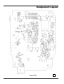
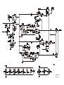
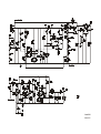
PSA1301T
1.3GHz Portable
Spectrum Analyzer
Service Manual
Manual Part Number 48511-1010 Issue 1
Table of Contents
Specifications
2
Frequency Measurement
2
Amplitude Measurement
2
Sweep
3
Signal Input
3
Demodulation (Zero Span mode)
3
Display
3
Memory Storage
4
Connectors
4
Power Sources
4
Mechanical
5
Environmental and Safety
5
Spectrum Analyzer
6
EMC
7
Spectrum Analyzer
7
Adaptor/Charger
7
Performance Definitions
7
General
8
Service Handling Precautions
8
Dismantling and Reassembling the Instrument
8
System Description
9
Control Board
9
RF Board
Servicing and Calibration
12
13
Control Board Test Mode
13
Charger Circuit Checks
13
Power Supply Checks and Adjustment
13
Microcontroller Flash EPROM Programming
13
Reference Oscillator Adjustment
14
Calibration Procedure
14
Parts List
16
Component Layout
20
Circuit Diagrams
21
1
Specifications
Frequency Measurement
Frequency Span
Frequency Range:
150 kHz to 1300 MHz (in one range)
Setting Modes:
Centre frequency plus Span, or Start frequency plus Stop frequency
Maximum Span:
1299.85 MHz (150 kHz to 1300 MHz)
Minimum Span:
320 kHz, or Zero Span with demodulation
Setting Resolution:
1 kHz at any frequency
Setting Accuracy:
Reference Frequency Accuracy for Start, Stop & Centre (Zero-Span) frequencies
Reference Frequency Accuracy
Initial Accuracy:
Better than ± 10 ppm at 20oC
Stability:
Better than ± 10 ppm over 10oC to 30oC
Ageing:
Better than ± 3 ppm per year
Phase Noise
Phase Noise:
Typically -100dBc/Hz at 100kHz offset at 500MHz
Resolution Bandwidth
RBW:
Selectable as 280 kHz or 15 kHz
Video Filtering:
Selectable independently of RBW setting
Frequency Markers
Number of Markers:
One, Two, or None
Marker Resolution:
0.1 kHz at all frequencies
Marker Accuracy:
1/320th of Frequency Span ± 0.1kHz + Reference Frequency Accuracy
Frequency Readout:
The frequencies at the marker points and frequency difference are displayed
simultaneously.
Amplitude Measurement
Amplitude Range
Display Range:
80 dB
Reference Level:
Selectable as -20 dBm or 0dBm
Amplitude Accuracy
Ref. Level Accuracy:
Better than ± 1 dB at 50MHz at 10dB below reference level (20oC ± 5oC)
Level Flatness:
Better than ± 1.5 dB relative to 50MHz over 500kHz to 1300MHz
Amplitude Linearity:
Better than ± 1 dB over 50dB range down from reference level
Noise Floor
Noise Floor:
2
Better than -90 dBm average displayed noise floor.
(reference level = –20 dBm, RBW = 15 kHz)
Distortion and Spurii
3rd Order Intermod.:
< –60dBc for two signals at 10dB below reference level (500MHz and 501MHz)
Harmonic:
< –60dBc at 10dB below reference level (100MHz)
1st & 2nd Image:
<– 55dBc, typically <– 60dBc
Residual Spurii:
Below noise floor
Amplitude Markers
Number of Markers:
One, Two, or None
Marker Resolution:
0.1 dB
Amplitude Readout:
The level at the marker points and level difference are displayed simultaneously.
Sweep
Sweep Method:
Peak detection for 320 points per sweep. The amplitude of the peak level found
within each sub-span is stored (sub-span = span/320).
Sweep Time:
Set automatically by Span and RBW.
Typically 200ms + 8ms/MHz of span (RBW = 280kHz)
Typically 200ms + 80ms/MHz of span (RBW = 15kHz)
Sweep Modes:
Normal (continuous), Single, Peak Hold, or Average (2 to 256 sweeps)
Sweep Control:
Separate buttons for Run and Stop. Peak Hold and Average are reset whenever
Run is pressed.
Signal Input
Input Connector:
SMA connector, 50 Ohms
VSWR:
1.5:1 typical
Absolute
Maximum
Input Level:
+ 20 dBm (2.2V rms) or 15V dc
Demodulation (Zero Span mode)
Demod. Modes:
AM or FM
Display:
Carrier amplitude only (horizontal line).
Audio Out:
30 mW into 32 Ohms mono or stereo headphones, adjustable volume, 3.5mm
jack socket
Display
Display Type:
3.7 inch (9.4 cm) transflective backlit TFT LCD, 480 x 320 pixels total, 16 bit
colour, touch screen.
Trace Area:
300 x 320 pixels (high resolution mode).
Graticule:
8 x 10 divisions light grey graticule. Selectable as fully on, horizontal lines only,
or off).
Displayed Points:
320 points per sweep (peak detected).
Live Trace:
Dot-joined trace from current or held sweep. Selectable on or off.
3
Reference Trace:
Stored trace either recalled from memory or copied directly from live trace.
Selectable on or off.
Resolution Modes:
Selectable as High Resolution or Low Resolution *
* In low resolution mode the trace area becomes 150 x 160 points where each point is a block of 4
pixels. Only 160 sweep points are displayed. This mode is useful in situations where the display
could otherwise be difficult to see - e.g. when the instrument cannot be viewed at an optimum
distance.
Memory Storage
Memory Type:
Non volatile Flash memory using removable SD or MMC memory cards.
Store Trace:
Any number of traces can be stored under either default file names or user
entered file names. Traces are stored as tables of amplitude versus frequency
and can be imported into other programs, as well as being recalled to the
screen.
Recall Trace:
Recalls any stored trace to the reference trace of the display.
Store Set-up:
Any number of instrument set-ups can be stored under either default file names
or user entered file names. All settings of the instrument are saved.
Recall Set-up:
Recalls any stored set-up, overwriting the existing settings of the instrument.
Store Screen:
This function copies the whole screen area to memory as a bit-map. Any
number of screens can be stored under either default file names or user entered
file names. Screen bit-maps can be viewed using the “Media” application of the
Palm T|X, or transferred to a PC for printing.
Connectors
RF Input Connector:
Standard SMA connector.
Power Connector:
1.3 mm dc power socket (centre positive) for 5.2V/1A external AC power
adaptor/charger as supplied by TTi.
USB Connector:
Mini USB connector (5 pin mini B) which provides direct access to the USB port
of the Palm T|X.
Audio Connector:
3.5 mm jack socket for demodulated audio out (accepts mono or stereo plugs).
Power Sources
AC Line Operation/Charging
The PSA1301T can be operated from mains power using the AC power adaptor provided by TTi. This
powers and recharges both the PSA1301 Spectrum Analyzer and the Palm T|X simultaneously.
AC Adaptor/Charger
Input Voltage Range:
100V to 240V nominal 50Hz/60Hz. Interchangeable plus for UK, Euro, USA and
Australia are supplied.
Battery Operation
The PSA1301 and the Palm T|X contain their own internal rechargeable battery packs. The PSA1301 is
turned off automatically whenever the PSAnalyzer program is exited, or when the Palm T|X is turned off.
4
PSA1301 Spectrum Analyzer
Battery Type:
Ni-Mh 3.6V 700mA-hr (3 x AAA cell)
Battery Life:
> 5 hours continuous operation
Recharge Time:
< 3 hours from fully discharged
Palm T|X
Battery Type:
Li-ion 3V 1050mA-hr
Battery Life:
Typically 4 hours continuous operation (depending on backlight brightness)
Recharge Time:
< 4 hours from fully discharged
Auto Sleep Mode
To conserve battery life, the system can be set to automatically switch into sleep mode after a defined
time from the last key press. This can be set between 5 mins and 60 mins (or never).
Mechanical
Size:
170mm high x 97mm wide x 47mm deep (including feet)
Weight:
495 grms total including Palm T|X.
Tilt Stand:
Built-in tilt stand for bench use which angles the unit at approximately 25
degrees to the horizontal and can alternatively be used as a hook mount.
Environmental and Safety
Operating Range:
+5oC to + 40oC, 20% to 80% RH.
Storage Range:
-10oC to +50oC
Environmental:
Indoor use at altitudes to 2000m, Pollution Degree 2.
Electrical Safety:
Complies with EN61010-1.
EMC:
Complies with EN61326.
5
Safety
Spectrum Analyzer
This instrument is Safety Class III according to IEC classification and has been designed to meet
the requirements of EN61010-1 (Safety Requirements for Electrical Equipment for Measurement,
Control and Laboratory Use).
This instrument has been tested in accordance with EN61010-1 and has been supplied in a safe
condition. This instruction manual contains some information and warnings which have to be
followed by the user to ensure safe operation and to retain the instrument in a safe condition.
This instrument has been designed for indoor use in a Pollution Degree 2 environment in the
temperature range 5°C to 40°C, 20% - 80% RH (non-condensing). It may occasionally be
subjected to temperatures between +5° and -10°C without degradation of its safety. Do not
operate while condensation is present.
Use of this instrument in a manner not specified by these instructions may impair the safety
protection provided.
WARNING!
All accessible parts will be at the same voltage as the outer body of the SMA input socket. In
particular, note that the shell of the mini-USB connector is galvanically connected to the body of
the SMA input which will therefore be at earth ground potential when the USB port is connected to
a desktop PC. To maintain user safety under all other circumstances it is essential that the input
is not connected to a voltage above 30Vdc or 30Vrms with respect to earth ground which is the
limit of Safe Extra Low Voltage (SELV) by IEC definition.
The instrument shall be disconnected from all voltage sources before it is opened for any
adjustment, replacement, maintenance or repair.
Any adjustment, maintenance and repair of the opened instrument under voltage shall be avoided
as far as possible and, if inevitable, shall be carried out only by a skilled person who is aware of
the hazard involved.
Do not wet the instrument when cleaning it.
The following symbols are used on the instrument and in this manual.
Direct Current
CAUTION – refer to accompanying documentation.
Damage to the instrument may occur if these precautions are ignored.
Adaptor/Charger
The adaptor/charger supplied has a universal input voltage rating of 100-240VAC, 50/60Hz. It is a
Class II (double insulated) device, fully approved to EN 60950-1 (2001), UL 60950 (UL listing
E138754) and AS/NZS CISPR:2002 (C-Tick).
6
EMC
Spectrum Analyzer
This instrument has been designed to meet the requirements of the EMC Directive 89/336/EEC.
Compliance was demonstrated by meeting the test limits of the following standards:
Emissions
EN61326 (1998) EMC product standard for Electrical Equipment for Measurement, Control and
Laboratory Use. Test limits used were:
a) Radiated: Class B
Immunity
EN61326 (1998) EMC product standard for Electrical Equipment for Measurement, Control and
Laboratory Use.
Test methods, limits and performance achieved were:
a)
b)
c)
EN61000-4-2 (1995) Electrostatic Discharge : 4kV air, 4kV contact, Performance A.
EN61000-4-3 (1997) Electromagnetic Field, 3V/m, 80% AM at 1kHz, Performance B.
EN61000-4-4 (1995) Fast Transient, 0.5kV peak (signal input), Performance B.
Adaptor/Charger
This AC adaptor/charger has been designed to meet the requirements of the EMC Directive
89/336/EEC.
Compliance was demonstrated by meeting the test limits of the following standards:
Emissions
EN55022, radiated and conducted Class B.
Immunity
Test methods, limits and performance achieved were:
a)
b)
c)
d)
e)
f)
EN61000-4-2 (1995) Electrostatic Discharge : 4kV air, 4kV contact, Performance B.
EN61000-4-3 (1997) Electromagnetic Field, 3V/m, 80% AM at 1kHz, Performance A.
EN61000-4-11 (1994) Voltage Interrupt, 30% reduction, 10ms, Performance B; 60%
reduction 100ms, Performance C.
EN61000-4-4 (1995) Fast Transient, 1kV peak (AC line), Performance B
EN61000-4-5 (1995) Surge, 1kV (line to line), 2kV (line to ground), Performance B.
EN61000-4-6 (1996) Conducted RF, 3V, 80% AM at 1kHz (AC line only; DC Output
connection <3m, therefore not tested), Performance A.
Performance Definitions
The definitions of performance criteria are:
Performance criterion A: ‘During test normal performance within the specification limits'.
Performance criterion B: ‘During test, temporary degradation, or loss of function or
performance which is self-recovering’.
Performance criterion C: ‘During test, temporary degradation, or loss of function or
performance which requires operator intervention or system reset occurs'.
7
General
Service Handling Precautions
Service work or calibration should only be carried out by skilled engineers.
Most of the integrated circuits are static sensitive and great care should be taken when handling
them to avoid damage due to static discharge. Also most devices are surface mounted
components with very fine leads on small pitches. These components must be removed and
replaced with great care to avoid damage to the PCB. It is essential that only the proper tools and
soldering equipment as recommended for surface mount components are used.
WARNING - Do not connect the power adaptor to the Control Board without the batteries being
connected first. Failure to observe this precaution might result in damage to the battery charging
circuit.
Dismantling and Reassembling the Instrument
WARNING – Disconnect the power adaptor from the instrument before dismantling the case and
unplug the lead from the battery assembly before removing any boards from the case. There are
no hazardous voltages inside the instrument.
The case consists of three main parts, the lower and middle sections, which are screwed together
and which house the spectrum analyzer hardware and the top section, which retains the PDA and
is clipped and possibly screwed onto the middle case section.
First remove the top section. This is achieved by pulling out the two recessed side levers that
hold it in place at the front (SMA connector) end of the case. If necessary, also remove the two
screws under the levers. Lift the top case section clear of the two location ribs on the back end of
the case.
Remove the PDA by pulling it off the connector that protrudes from the case mid-section, close to
the PDA buttons. Care should be taken to pull the PDA straight, without twisting, to minimise the
possibility of connector damage.
Remove the six screws that hold the case mid-section and lower section together. These are all
accessed from the top. Lift the mid-section off the lower section. The board assemblies can now
be lifted out of the case. Unplug the lead from the battery board and lift out the battery assembly
first. The Control Board, RF Board and PDA Connector Board assemblies are all screwed
together and are lifted out of the case together. Lift them upwards and backwards, releasing the
SMA connector from the front of the case and the USB connector from the side of the case. Note
that it might be necessary to bend the case wall slightly to clear the USB connector as it is moved
upwards.
The PDA Connector Board is attached to the back of the Control Board by soldered headers and
is only likely to need removing to replace the PDA connector. The RF Board and Control Board
assemblies are held together at one end by four screws and two hex spacers. At the other end
they are held together by a twenty way, single in line connector. The two assemblies may be
parted by removing the screws from one of the boards and then gently easing apart the twenty
way connector. This must be done without twisting to avoid bending the outer pins of the plug.
The RF Board circuitry is contained within screening boxes soldered onto the board and should
not be further dismantled except by the manufacturer. If a problem is suspected on this board,
the whole assembly should be returned to the manufacturer for repair or replacement.
When inserting the multi-board assembly into the case lower for re-assembly, first align the SMA
connector with the hole in the front of the case and then slide the assembly forward and down
into the case. The front of the RF Board has two slots which must be aligned with bosses in the
bottom of the case and the board made to sit on shoulders in these bosses. It might also be
necessary to bend the case side slightly to allow the USB connector to slide down.
8
System Description
PSA1301 is a frequency synthesised RF spectrum analyzer covering the range 0.15MHz to
1300MHz. The instrument has two selectable resolution bandwidths, 15kHz and 280kHz, two
input attenuator settings, 0dB and 20dB and two video bandwidth settings. Sweep times are set
automatically
The instrument consists internally of two main boards, an RF Board and a Control Board. These
two boards are connected together via a 20 way, pin and socket connector. This carries control
signals and power supplies from the Control Board to the RF Board and the RF detector output
signal from the RF Board to the Control Board. Attached to the back of the Control Board is the
PDA Interface Board, onto which is fixed the PDA connector. This link between the Control Board
and the PDA routes data and control communication, PDA charging supply and PDA USB signals.
A separate, rechargeable battery assembly is attached to the Control Board via a pluggable
two-wire lead. The battery assembly provides power for the spectrum analyzer hardware only. Its
status is indicated in the PSAnalyzer application by a battery icon alongside a similar battery icon
which shows the status of the PDA’s independent internal battery. The PSA1301 mains adaptor
charges both sets of batteries simultaneously via the PSA1301 power jack.
Circuit Descriptions
Control Board
Refer to control PCB circuit diagram.
The Control Board circuitry comprises a PIC® microcontroller†, post detection processing,
regulated power supplies and battery charging circuits. It also carries interfaces to the PDA and
RF Board and a flying lead for connection to the battery assembly.
Microcontroller and Associated Circuits
The microcontroller, IC1, contains all the code memory, data RAM and calibration EEPROM for
the spectrum analyzer firmware. It has several parallel I/O ports, which provide hardware control
outputs and hardware status inputs. In addition the microcontroller has three serial I/O ports.
These provide asynchronous communication with the PDA, serial control output to the RF
hardware and a serial data input port.
The microcontroller is capable of executing code to put itself to sleep, consuming very little
current until it is woken up again by serial communication from the PDA. The microcontroller will
go into low power sleep mode when there is no communication from the PDA. This will happen if
the PSAnalyzer application is not running on the PDA, or if the PDA is switched off or switches
itself off automatically whilst running the application, or if the PDA is disconnected. Before going
to sleep the microcontroller will put the rest of the Control Board into a low power mode by
switching off supplies and setting devices to low power mode.
The internal oscillator of the microcontroller provides a 4.608MHz system clock, which is used as
the reference frequency for the PLL ICs on the RF Board. IC2-A buffers the reference signal that
is passed to the RF Board. The 4.608MHz oscillator frequency is determined by crystal XTL1,
whose total load capacitance is provided by VC1, C6, C7 and IC8. VC1 provides coarse
mechanical adjustment of the oscillator frequency. IC8 is a digitally controlled variable
capacitance IC, which provides fine electronic adjustment of the oscillator frequency. It is
controlled via a serial interface comprising an enable signal driven by Port B bit 0 and a data line
driven by Port B bit 1. IC8 is programmed at power up and wake up by a series of data pulses
while the enable line driven high. The number of pulses determines the internal capacitance set.
9
PJ5 is the programming socket for the Flash EPROM within the microcontroller. It carries serial
programming data and clock lines on PJ5 pins 4 and 5 respectively and a +12V programming
voltage, supplied by an external PIC programmer, on pin 3. The I/O buffer circuits of the external
programming device are supplied from the Control Boards own +3V3 supply via pin 1.
The Control Board can be operated in a stand alone test mode by pulling PJ5 pin 5, and thus Port
B bit 6, to ground as the Control Board is powered up or reset (see Servicing and Calibration). In
test mode the microcontroller is inhibited from going into low power mode in the absence of serial
communication from the PDA and all Control Board circuits are kept powered up. This allows
Control Board measurements and adjustments to be made without the PDA being connected,
which can be difficult when working on the component side of the board without a special
extension cable between Control Board and PDA.
Pull up resistor R89 ensures that the Control Board does not enter test mode unintentionally at
power up.
R2, D1, R1 and C1 constitute a power on reset circuit.
IC7 is a DAC, which translates the analogue output signal from the peak detectors to serial digital
output. The interface to the microcontroller is via its SPI interface, which takes data in on IC1 pin
35 and provides a synchronous clock from IC1 pin 34 and a chip select from IC1 pin 58.
Q4 is the main power switch and switches power to all the measurement and RF circuits, via
+3V3S, under processor control. Q3 switches power to the FM detector on the RF Board when
FM demodulation is selected.
The signals PLL CLOCK1, PLL DATA1 and PLL STB1 bar constitute a serial control bus for the
1LO PLL on the RF Board, using one of the microcontroller’s USARTs in synchronous mode.
These signals are driven every time the centre frequency is changed.
PLL CLOCK2, PLL DATA2 and PLL STB2 bar constitute the serial control bus for the PLLs used
in the 2LO and 3LO on the RF Board. The signals are driven from bit ports and are driven at
power up, after a reset operation and when the spectrum analyzer wakes up.
POS PK SEL is a control signal, which selects the output from one of two hardware peak
detectors to be presented to the ADC for the measurement at the current display point. The
selection is based on a software display algorithm designed to render a more realistic noise floor
than can be obtained with a single positive peak detector. POS DET RES and NEG DET RES
control signals reset the positive and negative peak detectors respectively, as required by the
display algorithm, before the measurement is taken at every frequency across the sweep. BI-PK
is a logic signal driven by the peak detectors, which is used by the display algorithm for
determining which detector to select.
Audio Circuits
IC5-A, IC5-B select the output of the AM or FM detector as the demodulated signal to drive the
audio amplifiers. The AM detected signal is the RSSI signal from the RF detector on the RF
Board, buffered by IC10-A on the Control Board. The FM detector is a dedicated FM detector,
also on the RF Board. The selected audio signal is amplified by IC3-A and re-biased to centre rail
by IC3-B. The bias voltage is generated in the audio power amplifier, IC4. IC4 is put into low
power mode by a low level on the AUDIO SHDN bar signal when demodulation is turned off. The
gain of IC4 is adjusted to set the required audio volume. The gain is controlled via a two wire
interface consisting of AUDIO VOL CLK and AUDIO VOL DIRN. The gain is increased or
decreased by 3dB at each rising edge of AUDIO VOL CLK, depending on the state of AUDIO VOL
DIRN. If AUDIO VOL DIRN is high the gain is increased and vice versa.
The stereo jack PJ6 is wired to connect stereo headphone speakers in series. It will also connect
with a mono headphone plug.
10
PDA Interface
The PDA connects to the Control Board via a sub-board, called the Interconnection Board,
mounted on the back of the Control Board. The sub-board is electrically connected to the Control
Board by two six way headers, PJ2 and PJ3. PJ2 carries the asynchronous serial interface
signals between PDA and spectrum analyzer, TXD and RXD. D+ and D- on PJ2 and VBUS on
PJ3 are the USB interface signals of the PDA which are extended to the Mini-USB connector,
PJ1, on the Control Board. PDA_CHARGE is the supply to the PDA charging circuits from the
external power adaptor.
RSSI Signal and Peak Detectors
The RSSI signal is generated on the RF board as a continuous DC output from the logarithmic
RF detector. It is proportional to the instantaneous RF input signal level, in dBs, at the current
sweep frequency. The RSSI signal is low pass filtered on the RF Board by a series 1K resistor
and a 100pF capacitor to ground. On the Control board it is further filtered by C58, R77and C35
in parallel with C8. These components comprise the video filter. C8 is switched out of circuit by
IC13-B when WIDE VBW SEL is high, representing the video filter ‘OFF’ setting.
The RSSI signal is unity gain buffered by IC10-A. A DC voltage shift is also added by IC10-A to
optimise detector operation. The current through R23 determines the shift. Q1, Q2, IC11 and
associated components generate a constant current in R23 of approximately 1mA, which shifts
the RSSI signal by about +800mV.
IC20 and associated components form the positive peak detector. The peak value is stored on C2
and C3, which are charged via D6. Just prior to each measurement POS DET RES is pulsed high
and C2 and C3 are discharged to 0V by IC22-A. Simultaneously the input signal is disconnected
from IC20-A pin 3, which is then pulled low by R67. The detector starts to follow positive peaks
immediately after POS DET RES has gone low again. The voltage on C2 and C3 is unity gain
buffered by IC20B. This voltage is routed to the ADC, IC7, via IC19-A at the end of the
measurement period when POS PK SEL is high.
IC12-A compares the currently held peak voltage on C2 and C3, with the incoming signal. If the
incoming signal dips below the peak voltage then IC12-A pin 1 switches low. This is inverted in
IC9-A and is latched in cross-coupled gates, IC9-C and IC9-D. This latch is reset at the beginning
of the measurement period by the POS DET RES signal. Q11 and R21 form a constant current
source which generates a DC voltage in R3 to offset the detected peak voltage in order to reduce
noise sensitivity.
IC18 and associated components form the negative peak detector. Operation is the same as the
positive peak detector, except that the capacitors, C4 and C5 are initially charged to a +3V3 and
the detector records minimum signal amplitude after the reset pulse. IC18-B buffers the stored
negative peak voltage, which IC19-B routes to the ADC when POS PK SEL is low.
IC12-B detects if the signal rises above the stored negative peak signal. Current source Q10 and
R19 generate an offset in R18. IC21-A and IC21-C store the comparison result. If this logic latch
and the positive peak latch are both set then IC21-D switches the BI-PK signal high. This is read
at the end of the measurement period by the microcontroller. This informs the software algorithm
which peak detector reading to display at each point across the sweep.
Power Supply and Battery Charger
When the external power adaptor is disconnected or mains power is off, Q8 is turned on and
power is supplied to the instrument from the batteries. D9 and D11 are reversed biased. When
the power adaptor is plugged in and mains power applied, Q8 is switched off and D11 is switched
on, so that the analyzer is supplied directly from the power adaptor via D11. The batteries are
disconnected from the load and are charged by a constant current generator under the control of
IC6.
11
IC6 is a dedicated battery charge control IC. It senses the battery voltage via the resistor chain
R46, R47 and R48. The voltage at the junction of R47 and R48 represents one third of the total
battery pack voltage. The charge controller uses the ∆V method to determine when the batteries
are fully charged. LED1 is turned on when the batteries are being charged at the maximum rate.
Maximum rate charging is always enabled for approximately ten minutes when the power adaptor
is first connected and powered up. If the batteries are fully charged at the end of this time the
charge current is switched off else charging continues until they are fully charged. Fully charged
batteries are maintained by a pulse trickle charge, which turns on the full charge current for
286µsec every 8.86msec.
The constant current generator consists of pass transistor Q5, controlled by feedback amplifiers
IC30-A and IC30-B. A current sense voltage is generated across R38 which is differentially
amplified by IC30-A. The output of IC30-A is compared in IC30-B with a reference voltage
generated by R43 and D8. The comparator output drives the base of Q5 to maintain constant
current in R38. The ‘CC’ output from IC6 pin 8 is an open collector switch which IC6 uses to
control the charge process. The switch is connected to the comparator reference voltage at
IC30-B pin 6. All the time the switch is off the constant charge current is maintained. When the
batteries are fully charged the open collector switch closes and IC30-B pin 6 is pulled to 0V. This
turns Q5 fully off and the charge current is inhibited.
IC31 is a low dropout, linear regulator providing a +3V3 power rail. The reset button operates by
pulling the enable pin of this IC low, which switches off the supply, thereby causing a power on
reset when the button is released.
IC14 is a switched mode DC-DC converter designed to generate a negative rail equal in voltage
to the positive input rail. In this case the input rail is +3V3 and the resultant negative rail is
approximately –3V. The +3V3 supply is switched by Q9. When the Control Board is in low power
mode MASTER_PWR_UP bar is driven high and Q9 is switched off.
C44 and D12 steal some of the charge switched by IC14 and dump it into C45 which generates a
low power, nominally +5V, supply rail. D3 acts as a clamp to limit voltage surges on the +5V rail
during start up.
Q6, L3, D14, D13 and C47 form a flyback converter which generates a +15V varactor bias supply
for the RF oscillators. The +15V generator is supplied by the +3V3 rail, switched by Q9. A
relaxation oscillator consisting of IC15-A and associated components drives Q6. VR1 adjusts the
frequency of oscillation and thereby adjusts the +15V rail voltage up to the point where D13 starts
to limit the voltage.
† PIC® Microcontrollers are manufactured by Microchip Technology Inc.
RF Board
The RF board can only be repaired by the manufacturer. If a problem is suspected on this board,
the whole assembly should be returned to the manufacturer for repair or replacement.
12
Servicing and Calibration
Re-calibration of the instrument is required if the RF Board is repaired or replaced, or if any part
of the supply or measurement circuits on the Control board are repaired or the microcontroller,
IC1, is replaced.
Care must be taken when separating the RF Board and Control Board assemblies as the pins of
the twenty way header are easily bent if the connector is twisted as it is separated.
Control Board Test Mode
It is possible to operate the Control Board in a stand alone, Test Mode, without the PDA being
connected. Normally disconnecting the PDA will cause the Control Board to go into a low power
sleep mode with all supplies switched off except the microcontroller’s own supply. In Test Mode
this is inhibited and all Control Board circuits remain powered up. This allows basic DC
measurements and the oscillator adjustment to be made.
To place the Control Board in Test Mode a link must be connected between PJ5 pin 5 and 0V
when the Control Board powers up or is reset using SW1. 0V is conveniently found on pin 2 of
PJ5. The Control Board will remain permanently powered up until the power is cycled or SW1 is
pressed without the link in place.
Charger Circuit Checks
Operation of the battery charger can be checked in the following manner. Ensure that the battery
unit is connected to the Control Board before plugging the charger into the power jack. Switch on
the mains power. Regardless of the battery condition the charger LED should light for at least
10minutes (approximately), longer if the battery is not fully charged.
Measure the DC Voltage between TP4 and TP5 on the Control Board. When the LED is lit this
voltage should be 50.0 – 55.0mV, indicating a nominal 350mA charge current. Place a wire link
between PJ10 and PJ4 to force the charger into trickle charge mode. The Voltage between TP4
and TP5 should fall to a mean of 1 – 3mV, indicating that the mode has switched to trickle charge.
Note that this voltage reading might vary depending on the meter’s response to pulsed voltages.
Power Supply Checks and Adjustment
Check that the supply voltage at TP6 is +3.3V±70mV.
The following checks can only be made with the instrument in normal, powered up mode or in
Test Mode (see above):
The supply at TP8 should be +5V ±0.3V
The supply at TP7 should be –3V±0.2V
The +15V supply must be measured at TP9 under normal loading (nominally 1mA) and adjusted
using VR1 on the Control Board. The voltage at TP9 must be set to +14.6V±50mV.
Microcontroller Flash EPROM Programming
The operating firmware of the spectrum analyzer module is held in Flash memory within the PIC
microcontroller, which can be reprogrammed in situ. However, reprogramming requires the supply
to the PIC to be raised to +5V to overcome the code protection. To avoid damage to other
circuits, which normally run from a +3V3 rail, it is essential that the PDA, the RF Board and
the Battery Assembly are all disconnected from the Control Board BEFORE the external
+5V supply is applied. The external +5V is most conveniently applied to the wire leads of C15 ensure the correct polarity as there is no reverse voltage protection at this point.
Programming is done via socket PJ5, which is configured to conform to the standard
programming interface defined for the PIC. Refer to the relevant PIC information for details of the
programming interface signals and the Control Board circuit diagram to identify where the signals
are within the socket.
13
Reference Oscillator Adjustment
Final adjustment of the reference oscillator on the Control Board is normally done electronically,
on a completely assembled instrument, via the inbuilt software calibration procedure. However
after the repair of Control Board oscillator components or the replacement of IC1 it will be
necessary to make an initial adjustment using VC1 on the Control Board. This can only be done
with the Control Board out of the case and with the component side of the board exposed.
Operating the PSA1301 normally whilst having Control Board components exposed is not
possible without special interconnection cables. Therefore VC1 is most easily adjusted by directly
monitoring the reference oscillator frequency at TP12 on the Control Board using a frequency
meter, with the Control Board operating in Test Mode, as described above. Ideally the electronic
value should be previously stored as mid-range, using Step 1 of the calibration procedure (see
below). VC1 should be adjusted to set an oscillator frequency of 4.608000MHz.
Calibration Procedure
Equipment
TGR2050 RF Signal Generator - to provide 50MHz – 1300MHz, -50dBm - 0dBm, ten dB steps.
Spectrum Analyzer - 50MHz to 2GHz with frequency counter facility.
Alternatively:
Frequency Counter to adjust 4.608MHz reference oscillator as described above.
General
Calibration is performed via the instrument's built in calibration facility. The required input signal or
other brief instructions are displayed at each step of the procedure. The value of the internal
variable being adjusted is displayed with limit values displayed either side in brackets. To start the
calibration procedure, select the System menu and press Calib. The procedure operates on
temporary variables, which are set to the instrument’s current set of values on entry to the
procedure. The temporary values are adjusted throughout the procedure. Pressing the Set
Default key sets all temporary values to factory default values. When the Store Calib key is
pressed the temporary values are transferred to the instrument’s long term memory and become
the values used by the instrument during normal operation. Press the Exit Calib key to return to
normal operation.
Press the right navigator key to step forward through the procedure and press the left navigator
key to step back. Adjust variable values up and down using the navigator up and down keys. The
measured signal level is displayed in the M1 readout.
Step 1
This step provides an electronic adjustment of the internal reference frequency oscillator in a
closed case situation. Connect the test spectrum analyzer to the PSA1301 RF input socket and
adjust the value to set the leaked oscillator output to 2.000000GHz.
This step can be omitted if the alternative method of adjustment, using a frequency meter as
described in Reference Oscillator Adjustment above, was carried out successfully with sufficient
precision and care has been taken to ensure that the mechanical adjustment has not changed
since. In this case move straight to Step 2 without changing the value displayed in Step 1.
Step 2
Step 2, in conjunction with Step 3, performs an automatic gain adjustment. Input the signal
specified on the PDA display and wait for the displayed level to settle. Press the right navigator
key to move to Step 3 while the input signal is still present. If the input signal was found to be
outside acceptable limits then a warning message will be displayed. If Step 2 is exited with the
warning displayed, then the calculation for Step 2 will be abandoned and the temporary values
previously set up will be retained.
14
Step 3
This step completes the gain calibration started in step 2. Input the specified signal and wait for
the display to settle to approximately the specified level, this may take several seconds. Press the
right navigator key to move to Step 4 while the signal is still present. If the result of the internal
calculation is outside acceptable limits or Step 2 was not completed successfully then a warning
will be displayed. If Step 3 is exited with the warning displayed then the gain calculation will be
abandoned and the previously held temporary values will be retained.
Steps 4 to 9
These steps are all performed in essentially the same way. Input the specified signal at each step
and adjust the value until the displayed level in the M1 marker readout matches the level
specified. Move to the next or previous step when finished adjusting the value. Alternatively, store
the entire calibration at any point to permanently store the current temporary values from all
steps.
15
Parts List
PCB ASSEMBLY - CONTROL (44832-0300)
Part Number
Description
Position
22226-0170
KEYSWITCH - RIGHT ANGLE
SW1
22573-0322
HEADER/SPACER 20SIL 12MM
PJ10
22573-0323
HEADER 6W DIL 14MM 0.1P
PJ2-3
22574-0174
SKT 5 WAY SIL STRAIGHT
PJ5
22574-1030
SKT SM USB MINI-B
PJ1
22575-0077
SKT 2 WAY IDT
BATTERY PCB CONNECTOR
22581-0520
SKT JACK 1.3MM PCB
PJ4
22581-0530
SKT JACK 3.5MM STEREO
PJ6
23557-0686
CAP 470U 16V ELEC P5
C15
25061-0360
LIGHT PIPE LED RIGHT ANGLE
LED1
43187-1760
WIRE SET
PCB ASSEMBLY – CONTROL – SM STAGE (44832-0301)
Part Number
Description
Position
22156-3000
CHOKE SM2220A 220UHK 0.17A
L3
22315-1000
FUSE SM1206 500MA (F) 63V
F1
23101-1100
RES SM0603 100RF
R5, R20, R28-30, R32, R35-36, R43,
R65, R69, R105, R111-118
23101-2100
RES SM0603 1K00F
R11, R16, R22, R25-26, R39-40, R44-45,
R60, R71, R84, R86, R87, R106-110
23101-3100
RES SM0603 10K0F
R1, R9, R54-55, R61, R72, R76-77
23101-5100
RES SM0603 1M00F
R73, R81, R89
23104-0010
RES SM0805 0R15 W125
R38
23105-0012
RES SM0805 1R20F W1
R85, R88
23105-0470
RES SM0805 47R0F W1
R66, R70, R78-79
23105-1150
RES SM0805 150RF W1
R6, R37
23105-1240
RES SM0805 240RF W1
R24
23105-1470
RES SM0805 470RF W1
R3, R18
23105-1680
RES SM0805 680RF W1
R64
23105-1820
RES SM0805 820RF W1
R23
23105-2560
RES SM0805 5K60F W1
R19
23105-2620
RES SM0805 6K20F W1
R21, R57, R59
23105-3180
RES SM0805 18K0F W1
R50
23105-3270
RES SM0805 27K0F W1
R49
23105-3330
RES SM0805 33K0F W1
R2
23105-3390
RES SM0805 39K0F W1
R56
16
PCB ASSEMBLY – CONTROL – SM STAGE (44832-0301)/continued…
Part Number
Description
Position
23105-3470
RES SM0805 47K0F W1
R82
23105-3820
RES SM0805 82K0F W1
R41-42
23105-4100
RES SM0805 100KF W1
R4, R8, R12-14, R27, R31, R33-34,
R51-53, R58, R62-63, R67-68
23105-4270
RES SM0805 270KF W1
R46-48, R74-75, R80, R83
23105-4470
RES SM0805 470KF W1
R7
23384-2500
RES SM/PS/H 5K CERMET 4MM
VR1
23400-0100
CAP SM0603 10PJ 50V CER COG
C6, C7, C36, C139, C141-142
23400-0101
CAP SM0603 100PJ 50V COG
C24-29, C58-63, C65
23401-0104
CAP SM0603 100NK 25V CER X7R
C12, C17-23, C30-34, C51-54, C56-57,
C64, C67, C69, C70, C140
23405-0151
CAP SM0805 150P CER COG
C35
23410-0332
CAP SM1206 3N3J 50V CER COG
C2-5
23461-0015
CAP SM0805 10NK 50V CER X7R
C46
23461-0030
CAP SM0805 220NK 16V CER X7R
C48
23461-0040
CAP SM0805 1N0K 50V CER X7R
C49-50, C68
23461-0150
CAP SM0805 1N5 50V CER X7R
C8
23461-0500
CAP SM0805 4U7 6V3 CER X5R
C1, C9, C11, C13-14, C37, C41-45
23559-0010
CAP SM 100UF 6.3V AL ELEC
C38-40
23559-3470
CAP SM 47U 16V AL ELEC
C55
23595-0100
CAP SM-B 4U7M 16V TANT
C47
23985-0060
TRIMCAP SM 5-20P
VC1
25021-0010
DIO SM LL4148 SWITCHING
D1, D6-7, D10, D12
25031-1030
DIO SM ZHCS500
D9, D11, D14
25061-0304
LED SM0805 RED
LED1
25115-1010
DIO SM US1J 1A 600V 75ns
D15
25132-0220
DIO SM ZEN 4V3 W35
D8
25132-0280
DIO SM ZEN 15V W35
D13
25132-0310
DIO SM ZEN 5V6 W35
D3
25340-1000
TRAN SM PNP BC859C
Q7, Q10
25340-1020
TRAN SM PNP FZT751 60V 3A
Q5
25377-1000
TRAN SM NPN BC849C
Q1-2, Q11
25601-1010
TRAN SM FET P ZXM61P02F
Q3-4, Q8-9
25603-0220
TRAN SM FET N FDV303N 25V
Q6
27103-1040
IC SM LM393
IC15
27103-1100
IC SM MAX4232 R-R LV
IC3, IC10, IC12, IC18, IC20, IC30
27106-1480
IC SM LM4811MM AUD AMP
IC4
17
PCB ASSEMBLY – CONTROL – SM STAGE (44832-0301)/continued…
Part Number
Description
Position
27153-1120
IC SM MCP3201B 12 BIT ADC
IC7
27156-0170
IC SM MAX4643 DUAL SPST 8UMAX
IC5, IC13, IC19, IC22-23
27160-1050
IC SM V/REG 3V3 0.15A
IC31
27161-2040
IC SM V/REF LM385-1.2
IC11
27162-1060
IC SM TPS60401
IC14
27167-1000
IC SM BQ2002
IC6
27245-1474
IC SM MAX1474 DIG T/CAP
IC8
27246-0020
IC SM 74LCX02
IC9, IC21
27248-0040
IC SM 74VC2G04
IC2
27250-2160
IC SM PIC18LF6520
IC1
28500-2030
XTAL SM 4.608MHZ 10/10PPM
XTL1
35594-0170
PCB - CONTROL - PSA
PCB ASSEMBLY – RF (44832-0310)
Replaceable only as a complete module.
PCB ASSEMBLY – CONNECTOR (44832-0330)
Part Number
Description
20210-0100
NUT M2 ZPST
20234-0026
SCREW M2 X 5 PNHDPZ ZPST
22574-0810
CONNECTOR PALM TX
35555-4520
PCB - CONNECTOR - PSA
Position
PCB ASSEMBLY – BATTERY (44832-0320)
Part Number
Description
22010-0510
BATTERY 1.2V 700mAH NIMH AAA
22573-0247
HEADER 2 WAY STR .1P F/LOCK
35555-4630
PCB – BATTERY PACK
Position
MECHANICAL ITEMS
Part Number
Description
Position
20065-0020
SCREW M2.2 X 8 PLAS PNHDPZ
CASE UPPER/LOWER
20065-0170
SCREW M2.5 X 6 TORX PNHDST
20210-0104
NUT M2.5 ZPST
20234-0026
SCREW M2 X 5 PNHDPZ ZPST
20234-0026
SCREW M2 X 5 PNHDPZ ZPST
20234-0055
SCREW M2.5 X 6 PNHDPZ ZPST
20661-0291
SPACER Hex M2 x 8 NPBR
18
CASE UPPER/CONN PCB,
CONTROL PCB/M2 SPACERS,
RF PCB/SPACERS
MECHANICAL ITEMS/continued…
Part Number
Description
20661-0294
SPACER Hex M2 x 12 NPBR
20662-0550
FOOT - RUBBER 4280A
27740-1011
MEMORY CARD SD 64MB (MIN)
31547-0720
SCREEN SET
33143-0360
FOOT MOULDING
33143-0370
HOOK MOULDING
33143-0380
LATCH MOULDING
33536-4470
CASE - LOWER
33536-4480
CASE - UPPER
33536-4490
COVER TX PRINTED
37522-0160
LABEL SER NO - THURLBY-THANDAR
37541-1040
LABEL - CE
37541-1250
LABEL - WARNING - SMA
37541-1260
LABEL - MEM CARD
37541-1270
LABEL - DC INPUT
37541-1280
LABEL - SMA WASHER
43171-2580
CONN ASSY USB TYPE A/MINI B 2M
43171-2590
CONN ASSY USB A PLUG-A SKT
43912-0110
CARD READER SD READ/WRITE USB
48511-0870
INSTRUCTION MANUAL
48511-0880CD
CD - MANUAL/DRIVERS
48511-0950
LEAFLET READ FIRST
51151-0820
AC ADAPTOR PSA UNIV 5.2V/1A DC
61900-0010
PALM PDA TUNGSTEN TX
Position
19
Component Layout
Control PCB
20
4
Circuit Diagrams
21
Control PCB
Sheet 1 of 3
Control PCB
Sheet 2 of 3
Control PCB
Sheet 3 of 3