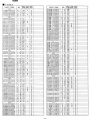
1
SHARP
SERVICE MANUAL
CODE: OOZMZ8OOIIIIE
PERSONAL COMPUTER
MODEL MZ-800
MZ-1P16
MZ-1E20
Table of contents
t,
2.
3.
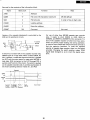
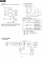
Specification ..
Parts identification ..
Systemdiegram ..
. .................................... 4
4.
Systemdescriplion ..
4·', Memorymep ..
................................................... 6
.. 9
4-2. CustomLSI .....
4-2-1.
Memoryconlroller ...
4-2-2.
4-2-3.
4-2-4.
4-2-5.
VOcontroller ..
Clock generator end timing generator ..
Display address generator ...
Scroll control circuit .....
9
9
. ....................... 12
.. ......... 12
.. ..... 13
. ......................................... 15
4·2·6. VRAMdeta inputloutpulcircuil ..
.............................................................. 20
4-2-7. Register functions ....
.. ........... 25
4-2-8. Pal1etcircuit .....
. ................................ 26
4-2-9. CRTC register map •.
4-2-10. ROMconfigufation ...
.. ............................................. 27
4-3. 8255 Programmable Peripheral Interface ...
......... ................................ 27
.. ...... 31
4-4. 8253 Programmable Interval Timer ..
. .................................................. 31
4-5. Printer interface ..
.................................................................. 34
4-6. Programmable sound generator .•
......... 35
4-7. Joystick ..
4-8.Systemswitchsetups ...
. ..................................................... 35
5.
Powersupply .....
MZ-1P16 .....
.. ......................................................... 35
. ................................................... 35
SHARP CORPORATION
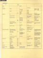
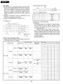
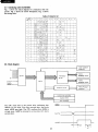
1 SpedfIution
-f-
t
IMl-700 - "'ItB
W.fJOO - 8ItB
CG
I;:' - :::....
Dicpl'vmethod
.CoIor
8'lm.p ..... thod
- Resolution
PCGmalhocl
... ,,..
320 >e 200
OP
320 >e 2OO
~~ >e 2OO
Colo< ..slgn .......1
Se'Mn.ndchl.KtIt
Se.Mn
~h'ndling
~_Ienc:oc*
M!~7~moo.only
~-
''''''''
10<121
10<121
180< '''', c:oIora
~0:010010
900'.ochltac:t...
~••• glnl"'ed-
---- ~of18co1ort;
_I---
- "'1t8
...,.
"'coIofl ChOHn out of
1ScaIO,.
~......tlon _+---+==",-~__ ~keOfI8caIO"
Cen"onlclinterl_
=:!.~-dtofd
~n~l~naISPllk"
~~
Cen"-Mitc:hldtaMl
interl_
P\o!point..
VI""'output
RF, VIDEO
C%rInCOderIPALI
'ThI1'lfmlna',oldd
,AnalagRG8woth
tI•• Ml-820FI
Joystick
~ -~
RS-232C
fO<IheRGBllrmlnl'
AlAR, compatibll
ijo'flitickdldlcatedl
I'ntlrlac.'
OP
----+TO':::._O"'"'
'- ......--,"'c----I'~""c:::"'2:::.:ii_
density
MZ-88,03
ATAAlcompat,bll
Joyllick
W-1E19,MZ·1Fl1
MZ.'0'lcomPl~
-o;;t;;;",,,ixp<lntlr
PlOt printer
:~'.:::",PI"~
Ml-1P18
St.ttu.SC£I011
_
~ilZ-800
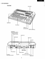
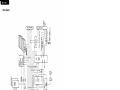
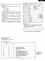
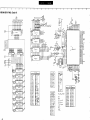
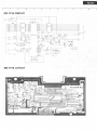
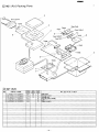
2. Parts identification
IFront view I
Data recorder
Definable keys
Main keyboard
POWER lamp
Cursor control keys
DELETE and INSERT keys
Channel knob
(home TV channel selection)
BW/color select switch
Composite connector
Expantion slot
RGB connector
RESET switch
Power input
External printer
output connector
EXT cassette jack
Joystick connector
Volum!! control
RF connector
(home TC cable connection)
Dip switch
MZ-1P16 power supply socket (+SV)
POWER switch
2
MZ-800
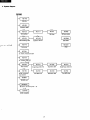
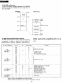
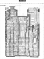
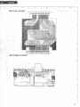
3. System diagram
MZ-1A18
AAMfile
MZ-1A25
Expansion RAM
MZ-1x17
MZ-1E19
MZ interface
MZ-1E20
MZ-1U06
1U06 interfacing PWB
Expansion VO box
MZ·1F11
MZ-6F03
MZ driver
MZ blank media
MZ-2Z046
DISK BASIC
MZ-1P16
MZ-2Z047
Plot printer
CP/M
MZ-1D04
12", 8-tone, monochrome CAT
MZ-1D19
14", 18-color, AGBI, CAT
/I~ 0,
'J).oh ,
MZ-1E05
MZ-1F19
MZ-1C30
MZ-1F19
M FD interface
Single floppy disk drive
Expansion cable
Single floppy disk drive
MZ-1T04
MZ-1F02
MZ-1C30
MZ-1F02
Expansion cable
Dual MFD drive
MZ-811 connection
tape recorder
Dual MFD drive
MZ-8BI03
AS-232C card
MZ-SOP5(K)
SO-column, dot matrix printer
25.
/1~
JOYSTICK
ATAAI compatible
3
MZ-800
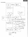
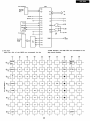
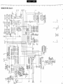
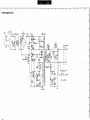
4. System description
16 KB
l
Basic RAM, 64KB
r---'
I
I
l.
r-
L _~
PPI
8255
-,
MZ-1P16
---
Plot printer
l
OP
I
,.--J
KEY
PlO
Z-80 PlO
CMT VF
MlSOP5K printer
Printer interface
CTC
8253
r----+----.J Joystick interface
(ATARI compatible)
PSG
RGBI
SN76489
CRTC
AMP
(Semi-cuslom)
MZ-1D19
o
VRAM
16 KB
rI
I
--,
MZ-1R18 slol
(dedicated)
I
I
r - -----,
I
Expansion slot-l
I
L
L ___ -.J
[2]'
MFD
_____
4
J
o
0
TV
HZ-1R25
)
--~
RS-232C
MZ-8BI03
MZ-1F02
I
VRAM
16 KB (OP)
Video
CJ1
1
OSCJ Cursor
556
Z-80A
GDG
·1
t...
LJ [
1
WE
&J
8253
DATA
RECORDER
AMP
II~~ ~
lci7Jt
PC21
~rl
CTC
Peripheral VO bus
CAS
RAS
CSROiI.1
I-
Option 16 KB
dn' ~
--c=
CONTROL BUS
DATA BUS
VRAS
OSC
556
VRAM DATA BUS
RESET
VRAM ADR. BUS
ADDRESS BUS
~CustomlC
t I~
cPU~
0= 3.547 MHz
RGBI
00
u
0"
u.,
~~~
'17.73 MHz
-~
Monitor,
SP
L--+_ _ _,
PA4
PA5
r
PAf
PBI
Z-80A
PlO
T
16KBROM
(27128
'I1L/"""'I
L\2-
fi
1""
w
c.
)(
0
."
'Cij
"
~
£
I
~
..)J
';~
~
System switch
(MZ +--+ Centronics)
~CTRLBUS
I~fl,--I~~--'-I
PRINTER DATA BUS
CTRLBUS
If
Bus driver
--ffi]
I
General purpose
input bus ' .~
J
JI
,I:'~::::::~i
External
printer
bus
,
iil
3
CD
Q.
.'
aJ
-
MZ-800
4-1. Memory map
The MZ-800 has a different memory map depending on
the mode. To have compatibility with the MZ-700, it has
two modes of the MZ-700 mode and MZ-800 mode.
o MZ-800 memory map
MZ-800 mode
MZ-700 mode
FFFF"
EOOO
~
~
0000
COOO
O[J D
AOOO
01000
--
MAIN
MAIN
o-RAM
o-RAM
64K.
64 KB
I
I
:
:
~
__ J
OVOR"';: __ , ,.--,
1
I
I
I
I n : lml: 1: IIV) II
L__ J 1 II
1
L __ oJ
~
640 )( 200 mode
320 x 200 mode
4000
NOTE:
,- __ .J
Item within dotted lin.
represents an option unit
~
O-RAM
1
:1 eX):1
~
1000
r--..,
1
r---,
2000
VRAM
ROM
VRAM
O-RAM
MZ·1R25
Memory map changes after initial program loading
® Power on
(resel)
MZ-800 mode
$0000
MON. ROM
SI 000
@ At start of monitor
© Wril. 10 PeG
MZ-700 mode
MZ-7oo mode
$0000 r - - - - - - ,
MON. ROM
$0000
$1000
$1000
CG.ROM
r-----;
from CG
MON. ROM
@ System operation
MZ-7oo & 800 modes
$0000
CG.ROM
$2000
$2000
DRAM
LD A, 08H
OUT (CE), A
$8000
V-RAM
(320x2oo mode)
=>
IN (EOH), A
DRAM
=>
D-RAM
D-RAM
IN (El H), A
~
SCOOO
DRAM
V-RAM (CG)
SDOOO
SDOOO
V-RAM
SEooo
MON. ROM
SFFFF
SEooo
SE010
I<.!'Y.
SEooo
SE010
nM~K
MON. ROM
V-RAM
MON. ROM
SFFFF
SFFFF
• Memory map at power on is in the MZ-800 mode as
in ®, but it changes to the MZ-700 mode by the
monitor ROM when the monitor program starts. After
transferring the CG data to the VRAM PCG area from
the CG ROM at @, the memory map then returns to
SFFFF L..._ _ _---'
• Depression of the manual reset switch assumes
memory map transition in order of ® ~ ® ~ @ ~
®, similar as in the case of power on.
• However, depression of the reset switch in conjunction with the I CTRL I key assumes the memory map of
@ after being changed once to the MZ-700 or MZ-800
mode depending on the state of the system switch. In
the case of the MZ-800 mode, it is set to the plane I.
IT (4-color mode) of the 320 x 200 mode.
®.
• When the system program is completed to load, the
memory map goes into the MZ-700 mode if the
system switch (SW1) is set to ON side. If set to OFF
side, it changes to the MZ-800 mode, then the
memory map as in @. During those changes, all
memory spaces are composed of RAM and isolated
from ROM and VRAM.
6
MZ-800
Memory Sank Control
~
port
MODE
Function
SEO
SEl
-
SE2
-
MZ-SOO mode
MZ-7oo mode
SE3
MZ-7oo mode
SE4
MZ-SOO mode
MZ-7oo mode
MZ-800 mode
o SOOOO - S7FFF o Soooo - SFFFF o SEooo - SFFFF o SOOOO - $OFFF o $0000 - SFFFF o SEooo - SFFFF o SOOOO - $OFFF o SOOOO - $OFFF
to DRAM.
to DRAM.
to DRAM.
to
monitor
to VRAM, key
monitor
monitor
monitor
to
to
to
ROM.
timer,
and
ROM.
ROM.
ROM.
monitor ROM.
o Slooo - $CFFF o Slooo - SlFFF
to DRAM
to CG ROM.
o Soooo - $FFFF o S2000 - $7FFF
to VRAM, key
and
timer,
and
$Cooo - SDFFF
monitor ROM.
to DRAM.
o $8000 - SBFFF
VRAM
to
(NOTE).
o SEooo - SFFFF
monitor
to
ROM.
i--l
0000
I
I
I
1000
2000
4000
I
I
I
I
I
5000
I
I
I
6000
I
I
I
I
I
I
I
I
I
I
I
I
I
I
I
I
I
I
DRAM
'--I 1--'
I
I I
I
I
I
I
I
I
MONITOR
ROM
I
I
3000
,---,
I
I
7000
8000
9000
Aooo
BOOO
COOO
Dooo
I
I
I
FFFF
I
I
I
I
DRAM
B
r-- - - (NOTE)
I
I
I
L __ ..J
V RAM
I
I
I
I
I
I
I
I
I
I
DRAM
I
I
I
Fooo
DRAM
I
I
I
I
I
I
I
I
I
I
EOOO
E070
I
I
I
I
MONITOR
ROM
CG
ROM
I
I
I
I
I
I
I
MONITOR
ROM
I
I
I
L __
DRAM
V RAM
V RAM
KEY, TIMER
DEY, nMER
MONITOR
ROM
MONITOR
ROM
MONITOR
ROM
J
Area within dotted line does not involve change.
(NOTE): In the case of 320 x 200 mode, contents of $8000 - $9FFF are transferred, instead,
and those after $Aooo are transferred to DRAM.
7
MONITOR
ROM
----1
Power on or RESET input
MZ-800
~rt
MZ-700 mode
MODE
Function
0000
1000
MZ-800 mode
MZ-700 mode
IN (SEO)
MZ-800 mode
MZ-700 mode
r--l I--l 1--' 1--, ,---,
I
I
I
I
I
I
I
I
I
I
I
I
3000
4000
5000
8000
I
I
I
I
MZ-800 mode
MZ-700 mode
9000
Aooo
I
I
I
I
I
I
I
I
I
I
MZ-800 mode
I
1
I
1
I
I
1
1
I
I
I
I
I
I
I
I
I
I
I
I
I
I
I
I
I
DRAM
(NOTE)
I
I
DOOO
1
I
Eooo
State before
prohibited
Prohibited
I I
I I
I
----
V RAM
(CGRAM)
Prohibited
I
V RAM
I
I
I
1
I
B B
I
I
I
r--,
I I
I
I
I
I
I
Booo
Cooo
ROM
1
,---,
I I
Q8
ROM
1
I
8000
R
1--,
I I
I
I
1
I
I
I
I
I
I
I
I
I
I
1
'1
Fooo
IN (SE1)
o SDOOO - S7FFF o SEOOO - SFFFF o SDOOO - SFFFF o SEOOO - SFFFF o S1000 - S1FFF o S1000 - S1 FFF o S1000 - S1FFF o S1000 - S1 FFF
returned
to
toCG ROM.
toCG ROM.
returned
prohibited.
prohibited.
returned
to
to
returned
to
the state be- o SCOOO - SCFFF o $8000 - SBFFF
the state bathe state bethe state bafore
prohifore
prohifore
CG
was
fore
CG
was
toVRAM (PCG
VRAM
to
bited.
bited.
set.
set.
RAM).
(NOTE).
o SCOOO - SCFFF o $8000 - SBFFF
to DRAM.
to DRAM.
2000
7000
OUT (SEe)
OUT (SE5)
1
State before
prohibited
I
1
I
L __ -.l
FFFF
8
I
I
I
I
~
I
1
I
I
I I
I I
I
I I
L __ -.lI IL __ .J
L __
I
I
J
MZ-800
4-2-2. 1/0 controller
In this I/O controller is created the select signal for
assignment of MZ-800 internal device.
See Table-2 for relation of internal device vs I/O
address.
4-2. Custom LSI
The custom LSI is a 100-pin single chip LSI on which the
MZ-800 memory controller (I/O controller) and CRT
controller, etc. are contained.
4-2-1. Memory controller
Used for the control of the memory bank. Addressing of
DRAM, ROM, and VRAM is conducted by selection I/O
address, $EO - $E6, using OUT or IN command.
I/O
address
Signal
name
Device (I/O)
Function
CPR
Z80A
PlO (I/O)
Port
Port
Port
Port
F2
PSG
PSG (0)
PSG output port
F1
FO
JOY
JOYSTICK (I)
Joystick-2 input port
Joystick-1 input port
FO
--
(0)
FF
FE
FD
FC
E6
1
--
--
(110)
B, printer data output
A, printer control and timer interrupt
B control (Mode 0)
A control (Mode 3)
Pallet write
Memory bank control
EO
D7
D6
D5
D4
D3
D2
D1
DO
C53
8253 (I/O)
Control port output
Counter-2
Counter-1
Counter-O
KEY
8255 (110)
Control
Port C, cassette, etc.
Port B, key input
Port A, key strobe output
CF
CE
CD
CC
--
--
0
I/O
0
0
$E008
--
--
I/O
(NOTE): Mapped to E007 - E004 in the
MZ-700 mode.
(NOTE): Mapped to E003 - EOOO in the
MZ-700 mode.
CRTC register
TEMP, HBLK input; and 8253 GO ON/OFF output for the MZ-700 mode only.
* When above I/O address is accessed, it makes 10WR active for OUT or lORD for IN command.
9
MZ-800
Pin
No.
1
2
3
4
Signal name
1/0
CPU
5V
GND
ADO
-
I
I
19
20
ADF
DTO
I
I
on
27
28
-----0--29
--30
GND
VCC
MREO
--
RD
31
WR
32
RFSH
33
IORQ
34
e----,.;----- I--Ml
35
---36- -SEL1
CASB
37
INH5
~8
f-----VBLN
39
1-- 40
GND
41
VRAS
42
IJCli:S
43
VADO
I
_._--50
51
52
53
54
55
Functional description
0
CPU clock (3.547 MHz)
Power supply
Ground
I
CPU address bus
1/0
CPU data bus
-
0
0
0
0
Ground
Power supply
CPU MREQ signal
CPU RD signal
CPU WR signal
CPU RFSH signal
CPU lORQ signal
CPU Ml signal
System RAM address multiplexer select signal
System RAM column address strobe signal
Inhibit bank (OUT $E5) select signal (uH" = Inhibit).
Vertical blanking signal
0
0
VRAM RAS control signal
VRAM CAS control signal
-
I
I
I
I
I
I
-
I
0
VRAM address signal (multiplexer output)
VAD7
VOE
VCC
GND
-
0
VRWR
0
VRAM output enable
Power supply
Ground
VRAM write signal
1/0
VRAM data bus (standard RAM)
1/0
VRAM data bus (option RAM)
0
0
0
0
0
0
0
Color sub-carrier wave
Video signal, red
Video signal, blue
Video signal, green
Brightness control signal
Vertical sync signal
Horizontal sync signal
Note
Negative logic
Negative logic
Negative logic
Negative logic
Negative logic
Negative logic
OPEN
Negative logic
Negative logic
Negative logic
Negative logic
Negative logic
VAO
I
I
62
VA7
VCO
I
I
--- 63--f-70
VC7
I----i ,-SBCR
--ii-- I---- RED
I----
--73--~---
BLUE
----GREN
1-----
75
76
YITN
77
f - - - -78
-----79
80
-_ .. _--81
HSYN
1-------
VSYN
-.
---
-8-2-
GND
VCC
CLKO
-
CROM
0
0
KEY
---a3- f------NTpL
-- --------f----
~~=p~SD~
86
-S7
lOWR
C---
lORD
-------aa-- --------cR S
89
90
f-- ----91
92
93
94
95
96
97
1------g8
99
100
SIO
RSTO
MNRT
---
PORT
I
I
I
0
0
0
0
0
I
I
C53
0
0
0
0
0
0
0
TEMP
I
WTGD
JOY
CPR
PSG
---
I
CKMS
53G
Negative logic
Negative logic
Clock input (17.7344 MHz)
ROM chip enable
8255 chip enable
NTSC/PAL selection (PAL - "L")
Test pin ("H" - test mode)
MZ-700/800 mode selection ("L" = MZ-700 mode)
Sum of CS and WR of 1/0 controlled by the custom IC
Sum of CS and RD of 1/0 controlled by the custom IC
1/0 $BO - $B4 chip enable
1/0 $F4
$F7 chip enable
Reset output
Manual reset input
Power on reset input
Wait signal to CPU
Joystick chip enable
PlO chip select
76489 chip select
8253 musical interval clock
8253 musical interval ONIOFF gate signal
8253 chip enable
MZ-700 mode, $E800 tempo input
* Term "OPEN" represents the signal not used on the board.
10
Negative logic
Negative logic
GND
GND
Negative logic
Negative logic
OPEN
OPEN
Negative logic
Negative logic
Negative logic
Open drain
Negative logic
Negative logic
Negative logic
Negative logic
I
MZ-800
Pin conflgur.tlon
m
TlM'
C&3
~G
CKMS
JOY
IIOIIT
IIISTO
CI"$
IOWR
TEST
KEY
CIJR
MOO MNIfT
SIC
lORD MOO'
Mm CJIIOM
.....
GNO
GNO
ADO
......
AOl
~TN
AD'
G"N
BlUE
•• 0
sac.
...
AD7
VC>
AOO
vet;
AOA
\IC4
VCI
ADO
VC,
ADC
VC2
AOO
VC.
AD'
VA7
\/CO
OTO
VAB
on
VAS
072
VM
073
VA3
0"
0"
VA2
VA1
.....
on
on
VAD
GNO
GNO
""IIJ
lO!SH
WJr
Custom LSI block diagram
lilT
~
~
SEll
VJIA!"
VI[R
[NHS
GND
VADO
~
VA02
VAD'
PORT MNRT
Clock generator &
timing generator
NTPL
--1
-
RD
WR
MREO
M1
10RO
RFSH
CROM
SEL1
CASB
INHS
VA07
I
CLKO
DTO -7
Vcc
2, 29, 52, 79,
pin
GND 3, 28, 40, 53, 78 pin
VAD6
VAOS
VSYN SBCR
HSYN VBlN CKMS
CPU
ADO - F
VA04
VADJ
•
RESET
-
CPU
DATA
.--
MOD7
~
8
CPU
VF
I
)~
R~iSplay contro
Input
BUFF
T
Rscroll
-
register~I--
Scroll circuit
~
I--
!
t
MPX
l
----
Pallet
circuit
CPR
KEY
C53
53G
JOY
PSG
CRS
SIO
lORD
10WR
110
RED
GREN
BLUE
YITN
VRAM address
controller
controller
1·
!
r
MPX
Shift
register
l
~
WTGD
TEMP
+
CONTROL
~
I
MPX
register
t--
Memory
controller
RSTO
Display address
generator
CPU address
,16
I
WAIT
controller
1 VRAM
-I Timing
control
1
1
VRAM data 110 circuit
8
VRAS
11
VCAS VRWR VADO-7
VROE
, 8
8
VAO-7
VCO-7
MZ-800
4-2-4. Display address generator
1) Display address generation
• Display address increments from left to right as
beginning from the home position at the upper left
corner of the CRT screen (address $000). The first
display line dominates address $000 through $027.
Because a screen frame consists of 200 rasters, the
address at the right side of the bottom corner is as
follows:
(200 x 40) - 1 = 7999 = $1 F3F
• The address counter stops counting for a horizontal
flyback line and stored in the address latch circuit.
When the horizontal flyback line terminates, the
address latch output is preset in the address counter
(display address generator).
• Address is generated even while the vertical flyback
line is active and it makes the counter reset before
termination of the vertical flyback line.
4-2-3. Clock generator and timing generator
Oscillation from the crystal oscillator is divided to create
the CPU clock, horizontal sync, vertical sync, and display address control signals.
Since the low state of signal is used for NTPL (NTSCI
PAL selection) with the MZ-800, the CPU clock of
3.547 MHz is derived from the crystal frequency of
17.734 MHz by dividing it 1/5.
NTPl
1>-----'
2) Display address generation in the MZ-700 mode
• Because characters are displayed under the PCG
method in the MZ-700 mode, address is generated
for each character and the same address is used for
displaying of one character. The 3-bit horizontal line
counter is provided to count horizontal lines to
generate the address (LCO - LC2) for selection of the
character front.
Display address increments from left to right having
the uppermost left corner of the screen for the home
position.
Since 25 lines are used to develop displaying of
characters composed of 8 x 8 dots, the address at
the right of the bottom lines becomes $3EF.
CK32 (112)
001 (114)
VSYN
To displ.-v .dd ..... generator
3) Display address multiplexed with CPU address
• Address used to write data to the VRAM is latched in
order to avoid CPU wait. Display modes of 640 dots
and 320 dots are assigned by the mode switch
(DMD2).
• Display address is multiplexed with the VRAM write
address in the timing of DISP which has the timing
that the display address and CPU address may
become a pseudo cycle steal.
Clock generator and timing generator circuits
OTO-7
ICPU dala)
IScroll regosted
,-----,
Scroll control
sw
SSA
IO,splay mode 'egoslll')
OM02
t>----+---'
Display address generator block diagram
12
I
MZ-800
4) Line scroll
SOF = $O~ $28
Programming "SOF = $28" makes the display screen
shifted eight lines up. Data on the highest line
therefore shifted to the bottom line.
Programming "$28 ~ $0" makes the display screen
shifted eight lines down, and the line on the bottom
moves to the highest line.
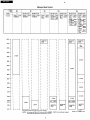
4-2-5. Scroll
1) Scrolling is possible for both horizontal and vertical
directions by means of software offset.
The following four registers are use~ for scroll
control.
a. Scroll start address register: SSA (7-bit)
b. Scroll end address register: SEA (7-bit)
c. Scroll width register: SW = SEA-SSA (7-bit)
d. Scroll offset register: SOF (10-bit)
5) Screen split
Appropriate deviation of SSA. SEA, and SW permits
to divide the screen into three sections of ®, ® and
I
(
©.
Though the section ® is permitted to scroll, sections
® and © are not permitted to scroll.
See the figure to explain with.
I
!
+--__
I
SEA
x y z
@
SSA-.
I
®
I
l,____
SEA-.
)
©
---
2) Control of scroll starts by the initialization of the
scroll control register.
SSA = $0
SEA = $7D
SW = $7D
SOF = $0
Assume now that the top of the section ® is on the
5th line (40 raster) and the top of the section © is on
the 18th line (144 raster). Attention must be paid to
the fact that values SSA and SEA are used for
assigning lines. Scroll registers are set with the
following values.
SSA = $19
SEA = $5A
SW = $41
SOF = $0
In this occasion, it needs to initialize the screen that
has been displayed. "SOF = $5" must be programmed to scroll ® one line. Then, only the section ® is
shifted up, and the highest line of ® moves to the
bottom line of ®. Programming "SOF = $A" makes it
scrolled one more line.
SOF ~ SW
Scroll offset (SOF) should necessarily be within a
range of the scroll width. Display is not assured with
SOF set greater than SW.
3) Way of smooth scrolling
SOF = $0 ~ $5
Programming "SOF = $5" makes the display screen
shifted one line up.
The highest line (address: $0 - $27) is then assigned
to the lowest line ($1 F18 -.: $1 F3F).
As normal scroll involves updating of the data for the
lowest line, the data of address $1 F18 - $1 F3F are
updated.
SOF = $5 ~ $0
By reducing the value of SOF by "5", it makes the
screen shifted one line down.
SEAL-____________________________
~
13
MZ-800
Scroll control register
SSA: Scroll start address
Increment of SSA: $5
Minimum value of SSA: $0
Maximum value of SSA: $78
Scroll and and control circuit hardware
• Block diagram
Scroll offset
Scroll width
Start address
MSB
LSB
N
6
3
4
5
2
SEA: Scroll end address
Increment of SEA: $5
Minimum value of SEA: $5
Maximum value of SEA: $70
SOF
LSB
MSB
N
c
SEA-SOF
10
DA(MA)
5
3
4
2
SW: Scroll width
Increment of SW: $5
Minimum value of SW: $5
Maximum value of SW: $70
Relation of SW. SEA. vs SSA
SW = SEA - SSA
SW> SSA
10
7
6
SEA
DA(MA)
7
MSB
LSB
N
6
5
3
4
S~ I
2
SOF: Scroll offset
Increment of SOF: $5
Minimum value of SOF: $0 (without offset)
Maximum value of SOF: $3E8
LSB
MSB
SOF 1
I
7
6
5
4
S~F I
2
3
LSB
MSB
SOF
21 __________
1
9
S~F
1
Relation of display address. SEA. SSA. vs SOF
Display address
m
SSA
6
SEA
6
SOF
9
SSA
SEA
SOF
j
I
k
SSA SSA SSA
4
3
5
SEA SEA SEA
4
3
5
SOF SOF SOF
7
8
6
i
h
SSA SSA
1
2
SEA SEA
2
1
SOF SOF
5
4
S~A
0
SEA
f
I
e
-
-
I
S~F IS~F
3
d
SOF
2
S~F
I
Screen left end address
o Line
1 Line
2 Line
3 Line
8
16
24
192
Line
Line
Line
Line
199 Line
0
0
0
0
0
0
0
0
0
0
0
0
0
0
0
0
0
0
0
0
0
0
0
0
0
0
0
0
0
0
0
1
0
1
0
0
1
1
1
0
0
0
0
0
0
0
0
0
0
Relation of SW vs SOF
SW> SOF
14
1
1
1
I
a
0
0
0
0
0
0
0
0
0
0
0
0
0
0
0
0
0
0
0
0
0
0
0
0
0
0
0
I
I
-
I
I
0
0
0
0
0
0
b
c
1
0
0
0
0
0
1
0
0
0
0
0
0
0
0
First line
Second line
Second line
Twenty fifth line
MZ-800
Concept of the scroll control circuit
Scroll method
• Scrolling by means of VRAM address conversion.
Execution of scrolling by address conversion
• Scroll offset (SOF) is the count of lines which the CPU
gives to the CRTC. For instance, the following must
be observed to perform scrolling.
3-line scroll: SOF3 = OF x 3
5-line scroll: SOF5 = OF x 5
And, to scroll one more line after 5-line scroll;
5-line scroll: SOF5' = SOF5 + OF = OF x 6
Range of scroll
• y-axis programmable.
BASIC console command compatible
• x-axis fixed
Scroll sequence
• The scroll start address is termed "SSA" and end
address "SEA".
• Execution of scroll, with offset given from the CPU.
• One line (line S) starting from SSA disappears from
the display screen.
• A new line (line S') is added to SEA. Line S' is the
same refresh memory as the line S. The contents of
the memory was erased (nullified by the CPU) before
the execution.
Display screen
000
SOF
SSA
t----''-------------i
A
Scroll screen
o
SW
SEA
1-----1
OB
IF400 (FAOO)
• Display address DA is the signal created in the CRTC
display address generation circuit and arranged in
their order from the upper left corner of the screen.
The bottom right address is 1F400 in the 640 x 200
mode.
• Display memory address DMA represents the VRAM
address corresponding to DA.
Since scroll is executed by means of address conversion, the order of DMA may not be the same as DA,
necessarily.
• CPU address MA is the VRAM address that obtained
from the CPU through the CRTC. To lighten burden
on the CPU, a circuit is added to make order of DA
identical to order of MA arrangement.
x
Fig-a Scroll area _ _ _ _ _ _ _ _ _ (640/320)
SS'/!
ABC
ABCDE
1234
1 23456
Line S
XYZ
~
VRAM
r--
~DMA
OPORSTU
9876543
Fig-b Screen before scroll
Fig-d Address conversion
-
SSA
ABCDE
4-2-6. VRAM data input/output circuit
1. Nothing intervenes for input and output of data in the
case of the MZ-700 mode.
2. MZ-800 mode
• Write
Read data (RD) from the VRAM and write data (WD)
from the CPU are subjected to logical operation
accordi'1~ to the direction from the write format
register (WF) and its result is written.
A BC
XYZ
OPORSTU
SEA
I-9876543
Line S'
Fig-c Line after scroll
15
MZ-800
• Read
For plane read data from the VRAM, data to be read
by the CPU are arranged in accordance with the
direction of the read format register (RF).
As the PCG method is adopted for the MZ-700 mode,
the text and ATB areas are actually mapped to $0000
- $OFFF. So, the VRAM address has the following
relation with the display character position.
1
2
3
40
:1:: 1 1-1
0001
11"'0 -1
~".n. t. 11 )
•.
======t=a
I
I
I
I
I
I
I
I
I
I
I
I
I
I
I
I
I
251
03CO
I I I -_-_~~~~
2) MZ-800 mode
As the bit map method is used for the MZ-800 mode,
it is possible to four screens of 320 x 200 dots and
two screens (maximum) of 640'x 200 data.
The cycle steal method is used for this mode.
i) 320 x 200 dots
See separate page for the timing chart duing
display and CPU read timing.
\/eo -1
tPlIMII.IJJ,IV!
* Logic circuit
Read data from the VRAM and write data from the
CPU are subjected to logical operation (OR, XOR,
RESET, etc.) and its result is used for the write data.
What i. p.eudo cycle steal
With the MZ-800, the pseudo cycle steal method is
adopted for VRAM accessing.
VRAM acee.. timing
1) MZ-700 mode
See separate page for display timing chart.
The VRAM is configured in the following manner in
this instance.
VA
LOAO~
x:~~.
I--
vc (option)
Not used
Not used
CG area
$3000
TEXT area
$3FFF
OISP. addr..s
OISP. clcle
X cpu address X OISP. add re..
I
CPU clcle
I
OISP. clcle
As shown in the figure, a next display data fetch and
CPU accessing are multiplexed during a display period.
Because accessing of the VRAM while characters are on
display causes the screen to blink with the MZ-700
mode, it awaits for blinking to complete before accessing of the VRAM. But, with the cycle steal method it
enhances faster screen processing as it enables to
access the VRAM during a display period. Because it is
not a complete cycle steal with the MZ-800 but timing is
taken using a wait in order to synchronize with the CPU
cycle for accessing from the CPU, it is therefore called
"pseudo cycle steal
$0000
$2000
===:x
u
ATB area
H
16
•
•
MZ-800
MZ-700 MODE DISPLAY TIMING
56.3ns
r=:
ClK
451ns
... 1
,'----
~--------------~,
VRAS
VCAS
VOE
,
''-_----'I
~
VAD 0-7
X
X'---'-'-'-''--''-'-----'
ATB. adr.
X 'ROW
X COL. X DUMMY adr. • X
X
---v----' '----------' __
ROW
COL.
'-----v-----'
~
-.J ' - - - -
CG. adr.
text adr.
------- --~C=>>----<C=>>--------<C=>>------<c=>>-----
VAO -7
'
lOAD
(shift register)
text DATA
CG.DATA
ATB. DATA
invalid DATA
,
...._ - - -
....
-----'
MZ-SOO MODE (320 X 200 dot)
ClK
\
VRAS
.
\
\
VOE
\
~
ROW
X
\
\
COL.
X
I (III) plane adr.
VCO -7
------
X
COL.
ROW
X
COL.
CPU adr. latch DATA
C=>>-------<C=>>-------<C=>>---------<
II plane DATA
CPU read DATA
---------C=>-----<C=>>-----<C=>~----------~
, ,
III plane DATA
lOAD
\
II (IV) plane adr.
I plane DATA
VAO - 7
CPU cycle
\
-.J
VCAS
VADO -7
.1 .
DISP. cycle
IV plane DATA
17
CPU read DATA
•
MZ-800
1) 320 x 200 dots
See the figure below for VRAM configuration and
CRT character display position.
VA
$0000
ve (option)
0
2
0
1
2
I
I
I
1
I
($1F3F )
Plane I
I
I
I
> Plane III
I
7999
Not used
$2000
0
2
0
1
2
I
I
1
I
I
I
I
I
I
I
Plane II
I
I
I
I
40
2
I
~
:I
I I
I
I
I
----hd
I
I
I
---"DJ
3
;I: I
I
40
I
I
I
I
I
2
I
I
2~ 17960
7999
----
(Raster)
eRT display position
Plane IV
I
I
I
7999
Not used
$3FFF
2) 640 X 200 dots
Because it operates in the cycle steal mode, two
bytes of display data are fetched during one byte
display cycle. (See the chart in separate page.)
See the figure below for VRAM configuration and
CRT character display position.
$0000
0
2
4
I
I
I
80
I
I
0
2
4
I
I
I
I
I
I ' I ' t'--l--H
I-~EJ
2
o
2
80
3
4
__
I
I
I
I
I
($1F3F )
$2000
I
15988
Not used
1---, --3
5
:
79
I
I
I
I
I
I
--,--3
:,
200 "'-159-20--1---+-1
I
I
~:::::::::::::::::: i' ' ' I
eRT display position
I
I
I
I
I
I
($3F3F)
80
15999
Not used
$3FFF
VA
ve (option)
(Plane I)
(Plane Ill)
18
•
MZ-800
800 MODE (640 X 200 dot)
DISP. cycle
-I·
,'---___----~I
VRAS
VA 0 - 7
0 - 7
~
ROW
X'____CO_L_.----'X'____C_O_L._~'C~'___ _ _ _ _ __:_--~X
'---;;~
'------C~
N+1th adr.
I plane N+l th DATA
X'-__--,--_
~===N=+=-2th~ad-r.~~
cPU read DATA
----------~~~----~~~----~<==>~---------------~
III plane Nth DATA
1II plane N+ 1th DATA
CPU read DATA
LJ
CPU and VRAM accessing
1. Accessing of the VRAM by the CPU is carried out in
the cycle steal mode (MZ-800 mode only) during the
flyback period of the display under the control of the
CRT controller.
2. Even when there is no accessing from the CPU in the
CPU cycle, such as VRAS, VCAS, VOE, etc. are
outputted in the timing of the read cycle at all times.
3. Write to the VRAM is carried out after logical operation of the read and write data by means of the
read-modify-write method. But, in the case of the 320
x 200, 16-color mode, data are written in two CPU
cycles as there is a need of writing to Plane IV.
See separate paper for timing chart.
4. CPU wait
1) Write
• As there is a one-byte buffer in the CRT controller,
write to the VRAM from the CPU is carried out
through the buffer. But, actual write to the VRAM is
~VRAS
-.J
VCAS
~
V OE
~
VADO-7 ~
cpu cycle
<D
done by the CRT controller. Therefore, there would
be no need of wait under almost any condition in the
MZ-800 mode.
• Even in the MZ-700 mode, wait is issued when there
are more than two writes in a display period.
Display period
HBLN
~r-.-----------1.l"'- ______
WAIT
------------4,,\'- _ _ _ _ _ _".)r.
)l"----J
~t..._J
2) Read
Wait is issued along with the CPU write action both
during displaying and flyback periods to perform
reading operation in synchronization with the CPU
cycle.
cpu cycle@
DISP. cycle
-I-
Flyback period
~:~~w:R-----LJ~<D~-----t-L----~®l--,~rl-,-:-----<D@
..- - - - - - . - - - - - - - -
- _ .r - '.~
I
- - - - - - - - - - - -
\
\
r
\~-----------
\
\
ROW
COL.
X~~~======~----x'--~~==x~====~x===~~~x
CPU adr. latch DATA I. III plane
DISP. adr.
ROW
X'--__C_O_L._ _ _ _ _ _ _ _ _X
11. IV plane
L-.J
VRWR
----~CJ:J___{
read DATA
VC 0,-7
,
-------~~~----~~~----~<==>~------------------~
LOAD
(sift register)
VA 0-7
\'-----
,'-------/
I plane N th DATA
vc
\'-----
\~-----------~
VOE
VAD 0 - 7
DISP. cycle
-I·
\~-- __----_~I
''---~
\'---~/
VCAS
CPU cycle
-----~
)>--------<c=::)>-----c=>-~
I plane
write DATA
1II plane
)>---------<c=::)>-----c=>>-----QD---(
19
DISP. DATA
IV plane } - -
MZ-800
4-2-7. Register functions
VRAM configuration
• One or two chips of 16 KB VRAM are used.
• In the case of a single 16 KB VRAM chip, it handles
320 x 200 dots, 4 colors, or 640 x 200 dots 1 color.
• In the case of two 16 KB VRAM chips, it handles 320
x 200 dots, 16 colors, 640 x 200 dots, 4 colors, 320 x
200 dots, 4 colors, 2 frames, or 640 x 200 dots, 1
color, two frames.
•
DMD 3, 2: Display method and resolution
DMD
2
3
o
o
I
o
1
-----~--
-i
next are about functions of the custom LSI.
There may be some restrictions because the standard
version of the MZ-800 incorporates only one 16 KB
RAM.
•
I
MZ-700 mode
----------------+------------------------~~-----
I
1
Prohibited
DMD 1, 0: Display screen designation
DMD DMD
1
0
Display mode register (OUT &HCE)
• It consists of four bits which are used to represent
display method, resolution, and display screen (color
plane) in combined way.
Bit map, 64~~ _____ _
I
1
0
1
* Discussed
Bit map, 320 x 200
I
320 x 200
640 x 200
Frame A, Plane I
Frame B, Plane ID (NOTE)
Planes I, m
0
0
1
0
1
0
Frame A, Planes I and n
Frame B, Planes ID and IV
Planes I, n, m, and IV
1
1
Prohibited
MZ-700
-~=
Normal
Prohibited
Prohibited
I
m, not Plane n.
NOTE: 640 x 200, Plane B
IS
Plane
• With the MZ-800, DMD 1
~
0, DMD 0 = O.
Display mode register (DMD)
Table-' VRAM configuration and display mode
VRAM
~:~~c~
VRAM configuration
Resolution
_________~___. ~_~______
_I : ItIVTI'
1
320 x 200
I
i
Display
Display
Color combination
0010'
'"me
(NOTEI
140010<5,
F"mJ I. n
DMD
__
'I
3
2
__
I0
0
1
0
0
I 0
16 KB
640 x 200
8000 H
f----
~ ~_B_F_F_F
___
-----llltl
""'" I
I 11
-=-~
H
32 KB _ _
8000
j
"
r-Ll
GGG
on
"
T'
vcr
0 G
t
I
BFFF
IF"me
-VA-0--7--vc-o-.,
III
320 x 200
140010<5
+;---1l~ -~o 1~+-;
l
n
~-i -~ +r~-
(eme B 1rn,
0
1'6 0010<5 IF"me ~I. ~~-f
r
-- ---
-t-------+--~t-
I _1_'
0
~010' l:am~-____f--~---1-l-~~---~I-~ame
640 x 200
i
I[
+.1.
!
B
I ill
11--------
i,l
I
4 colors Frame A I I. ill
+----:-
~-~-- --------------~~---------~ I ~0-2-c5-h-~r-nae-cs-te-r-s-t-II-8 0010<5 !"me A IAGB
(NOTE) Except for the MZ-700 mode, actual display colors are produced by the pallet.
20
I 0 i 1 I 0
1
i
I
!
i
I ---1---1-----+---I
I
I
i 1 i 1 i 0
I, fo T~ i;i
I
0
!
I
:
MZ-800
VRAM to CPU interface
• SRCH/S I NG
"0": Single color data read .....
Reads the data of the color plane, 1, IT, rn, or N,
specified by "1 ".
NOTE: Only one item should be "1" out of I, IT,
rn, and N. If it is "1" for more than two or
non-existence of the VRAM may not
assure the data read.
"1": Specified color search .....
"1" is retu rned for the bit of the color specified by
0/1 of I, IT, rn, and N.
NOTE: Depending on the display more, color
combination is permitted for the bit combination of L IT, ID, N; ID, N; I, IT; I; and
ID. Bit combination otherwise will be disregarded.
(ex. For the 640 x 200, 4-color mode,
combination becomes possible for I and
ID, and IT and N are disregarded.
• As the CRTC bus is completely separated from the
CPU bus, read and write of the VRAM is carried out
through the CRTC. Therefore, interfacing with the
CPU is done via the read register or write register in
the CRTC.
• VRAM access by the CRTC is done under the pseudo
cycle steal mode.
• Not only read and write are for the accessing with
the CPU, it permits to read multiple number of screen
data logical operational results and to write the
read-modify-write of the logical operational results
for the data already written. So, it has two registers
of the read format register and the write format
register.
• It permits CPU access to the non-display plane in the
display mode according to the BI A bit and it enables
selection of data buffer and two screens, when the
32 KB VRAM is used.
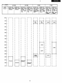
a) Read format register (RF) (OUT & CD)
LSB
MSB
SR~I:G r~",r'''~] ~A
I
• B/A
CPU access plane change
MZ-800 ---> "0": Frame A access .....
Accesses the frame A (planes I and IT for the 320
x 200, 4-color mode; plane I for the 640 x 200,
1-color mode).
"1": Frame B access .....
Accesses the (planes ID and N for the 320 x 200,
4-color mode; plane IT for the 640 x 200, 1-color
mode).
I
IV
!
11
III
* NOTE: Same as the bit B/A of the write format register.
• L IT, ID, N ..... Color plane designation.
21
I
f
I
!
MZ-800
Table-2 Display mode vs read format register
Display mode
SRCH/SING
B/A
IV
m
n
Function (NOTE)
--------------r---------------+--------+---------~----~----_+----_r----~--------------------__i
320 x 200.
4116 colors
Single color
data read
Frame A: "0"
o
o
o
o
o
Plane I data read
o
n data
Plane
read
~--~-----+-----+----~-----------------------
Frame B: "1"
640 x 200.
1/4 colors
o
o
o
m data read
o
o
Plane
o
o
o
Plane IV data read
-----------~--------------~---------~--------_+----_+----~----4_----+_--------------------~
x
x
o
x
x
o
x
x
x
x
o
o
o
320 x 200.
4 colors
o
o
Specified color
search
320 x 200.
16 colors
x
I,
o
n
dot search
dot search
T. n dot search
L
n dot search
x
x
m.W dot search
x
x
m. W
x
x
m. IV dot search
x
x
m. IV dot search
o
T.1f.
o
m. IVC dot search
L1f. m. IVC dot search
o
T. n. m. IV. dot search
I. n. m. IV. dot search
o T. n. m. IV. dot search
o
o
o
o
o
o
o
o
o
o
o
T. n
dot search
n. m. IV. dot search
1
1
1
1
L
x
x
x
0
T. dot search
x
x
x
1
I. dot search
x
0
x
x
m. dot search
x
1
x
x
m. dot search
x
0
x
0
T.
x
0
x
1
m. dot search
L m. dot search
x
1
x
0
T.
x
1
x
1
m. dot search
I. m. dot search
0
0
0
1
Data. ATB. CG area read
0
640 x 200.
1 color
1
1
c--640 x 200.
4 colors
-----
1
x
-~-.---
MZ-700
0
0
(*): Refer to the display frame of Table-1.
NOTES:
•
Read for the non-existing VRAM are not assured .
• The above parameter has to be set up for the MZ-700
mode.
B/A must be set to "0" for the standard MZ-800
(without MZ1 R25).
*
22
MZ-800
b) Write format register (WR) (OUT & CC)
• WMD 0 - 2 .....
Selects the logical operational mode for readmodify-write .
•
•
rn,
I, Il,
IV .....
Color plane designation
Write
mode
'2
-SINGLE-- . +- 0
WRITE
WMD
1
0
0
0
1
o r --tr0-
EXOR
----t-- -
OR
o I __
RESET
0-1
~
1-
B/",:
IV
0/1
(*)
~
Frame A: 0
11
---j
01 Frame
Color plane
ill
IT
-~
Function
0/1-
I o~T, ~/~ +,1,'~/01, ,--
t---r-
OIl
I
--;1
B: 1:_~/~ .j,_~l_i_ 0~~0/1:
I
1
B/A (NOTE)
Standard MZ-800 ---> "0": Frame A access .....
Frame A is accessed for the display mode.
"1": Frame B access .....
Frame B is accessed for the display mode.
[WD: Write data
VD : VRAM data
1
-----lc~~~I-;ne of;;1~WD, wri;---------
320 x 200,
i
4/16 colors
jcolor
,Color plane of "0": Fixed
640 x 200,
1/4 colors
Color plane of "0": Fixed
pl~~~--;:;-0Y-WD <:BVO-------I---~' ---------- -------.-------
ll~-:;~~;~~ ~:~~:::F~; VD ______ _
-,1 -~ -Iu=i=- ('F~:: i ;;;;:-;oo@, !:;;~~:~~';:f::~~,:::',:,O;--' ------I
'L
o
iColorplaneof"l":WD.VD
1
_
r-~--. 0/~_+0/-1_·1i _ x--~--~"li ~2~I:r~o~_~ (Character write to the graphic plane)
I
REPLACE
,I
x i_.
x
0 __
I,
0/1 i~ OIl
I
OIl i, OIl ,I.
.'
16 colors
II Color plane of "1": WD
---l+I---x-i--lI----~--t~ ! 0/~r~4~-=-;~ ®, 1Calor plane of "0": Writes "0".
J __><....t~~><_l_~l-~~olor ~ Calor plane of "X": Fixed
I ___~ __
i
I
x
I
x ,011 I x i OIl!
640
x 200,
!
to-~~_--- I ~-t-~~ i i 132: :o~:~s ®, -r-~rites
I
f-~ _9Q .<>'~J.-~-' -i-- ~<:<>Iors ~
1
0/
0/1
1
x
PSET
I
I
x
___
x
I
I
OIl
11
0/1
t'I OIl T;1
I
I
3~~ cox 1200
,
ors
only-bi.t "1
~:-~-;-~~ i;;~pecific
calor.
(Character write to graphic plane)
I Calor plane of "1": WD + VD
1
r- - "0-- -r -;-:--~- -;-1o~1 ~~~-;;-~®~-! Calor plane of "0": WD· VD
r- - - 1 - - ~ x OIl 1 x ! x 1 calor, ® ! Calor plane of "X": Fixed
I
--"'-r-- - ----r----t------I
,
I
MZ-700 1
0
o
I
x
i x : OIl
__+-_____ ! _ 1I
1I
o
I 0 I 1 I
0
I
0
I
0
I
x I OIl!
I I
(*) Refer to Table-l display frame
NOTES:
• Write for the non-existing VRAM are not assured.
• The above parameter has to be set up for the MZ-700
mode.
• BI A must be set to "0" for the standard version
MZ-800.
23
640 x 200,
4 ~?Iors
MZ-700
i
1
11
.
_____ _
' Writes WD into the DATA, ATB, and CG area.
MZ-800
CD REPLACE
c) Example of CPU read/write access
• Shown next are access examples of REPLACE write,
PS ET write, and SEARCH read in the 320 x 200,
16-color mode.
As for display colors, Plane I corresponds to 8, IT to
R, ill to G, and IV to I.
write
• To develop light yellow characters on the graphic
screen.
Plane I (B) data
Bo 01° 1'1'1'1' i COTo i '1' °R~
1
1
V
R
A
Plane III (G) data
M
Display before write
It develops the screen when a next CG patterns are
written after setting the REPLACE mode and the light
yellow color in the WF register.
Mode
WF register
Plane 11 (R) data
So, the bit "1" of the write data becomes the color
specified by WF and rest of others become RESET
(black).
BlA Calor designation
~-O--o=r!]
,
, --oJ:
Write data I
(CG pattern) ,~-----
°
Light yellow replace mode
V
R
°
Plane I
Plane 11
I ° 1°lolol~liEJ
10t'lol'[0] , ! ° I' I
Plane III
Plane IV
A
M
Display after write
°
1° I , 1° I' I ° 1' 1°liJ 1° I' 1° 1' 1° I' 1ON
® PSET write
• To overlay a light yellow hatching over the graphic
display screen of CD.
Mode
WF register
BlA Calor designation
'- 1_,___0-- '1_0-- -'-1_,_____0_1 :
G
Write data
~
°
R
Light yellow PSET mode
B
°
I (B)
V
Display after write
R
A
M
° 1° 1° 1° I' 1° 1' 1° I I ° 1' I' I' 1° I' I' I, 1
III (GI
1° I' I' I' I'
So, only the bit "1" of the write data becomes the
color specified by WF in this mode, and rest of other
colors do not change.
RF register
1° I' 1° 1' 1° I' 10 I' 1
1° ° ° 0' I:
I' 1° I'
L . -_ _ _ _ _ _ _ _ _ _--'
Only the bit of light yellow
becomes ",",
• When the above read data are read after setting the
red PSET mode in the WR register.
...
<J
" I 0~
en'" a:1= "a:
i~
BlA Calor designation
LI_,_IL-_----'-I_o_--'-I_,____o---'I :
IV(!)
Read data
@ SEARCH read + PS ET write
• To change light yellow in ® above to change to red
• The following data are set when the memory is read
after setting the light yellow search mode in the RF
register.
Mode
11 (RI
Light yellow search
24
Cl)
Cl)
'"co
'"
'"
::;;
'"
"a:
Cl)
~ 1a:~
1t
u
j
Now, a partial color change has been attained.
As in above, it enhances fast display change with less of
VRAM accessing by using various write modes.
MZ-800
<Pallet register write> (FO H )
4-2-8. Pallet
• As there are four 4-bit pallet registers provided inside
the unit, it permits choice of R, G, B, and I combinations, and it enables to make choice of any desired
two or four colors out of sixteen available colors.
However, in the 320 x 200, 16-color mode, choice of
colors permitted to four kinds of colors output of
sixteen.
• Only the conventional mode is applicable for the
MZ-700 mode without using pallet.
• Pallet is not applicable for the border color.
(FO H )
OUT FO H
DB;
SW;
Bo
B,
PLT2
B,
B,
SW,
Ro
R,
R,
R,
~
~
~
f
DB,
G;
G,
G,
G,
3
0
B output
:
R output
~~~~;~ut ---0 ~
~
Plane III
SA
output
DB,
Plane 1\-
01
~
G output
"-l.o-
I output
--0 I
I
SA output --0 :
So S,
A
Inpu! select Signal
B
320 )( 200,
Output select Signal
SWQ, 1
S,
So
Register No.
0
0
0
PLT 0
0
0
---
PLT'
PLT 2
0
,
,
- .01
1
PLT 3
1
0
0
SWo• SW,
.-
---
2) Bi, Ri, Gi, li: Pallet write data
3) SWo, SW,:
With these switches, it is possible to make combination of Planes ill and N data in the 320 x 200,
16-color mode. Switches are used to assign pallets to
four groups of colors.
(Plane ill data) = SWo, (Plane N data) = SW,
Only for the color information, the color information
set by the pallet register are available as B, R, G, and
I outputs. For color information other than that, data
in Plane I through Plane N are sent out as the B, R,
G, and I outputs.
(See example next.)
PLT3
~I~~:;PUI --0
0
DB,
S2
0
enable
PLTl
S2
x
-~-
Pallet
PLTO
I
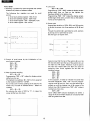
1) So - S2: Register section
<Configuration>
SWitch
LSB
MSB
Plane III 1\
SR output
<Pallet output and display mode>
• Shown next is the relation of the display mode, color
plane data vs R, G, G, I outputs.
Pallet output select
Display color
Display mode
Frame A
4 colors out of
16 colors
A
SWo• SW,
B
Plane n
data
Plane I
data
Output select
Pallet enable
x
Frame B
4 colors out of
16 colors
Plane ID
data
Plane IV
data
B
o
o
o
Bo
1
B3
o
o
Bo
o
1
B2
R2
G2
12
1
1
B3
R3
G3
13
0
0
Bo
Ro
Go
B,
10
R,
G,
I,
o
4 color
320 x 200
Output Output Output Output
A
x
Go
I
10
f----+-----+---4----- -----+-----1
SW =
o
(Ex.)
16 colors
16 colors out of
16 colors
Frame A
2 colors
I
I!
data
SW = Plane IV
'
(data
)
10
_+ __----1
I~~_~-~-ti-:-:-+--:-:-~-~-'~--::~
2
B3
R3
G3 I 13
~---------+--x-4-X-~-I--~-IT-+--ID---+-IV~
Plane I
II
x
x
! 1
I 1
Ir---0_
x
Bo
Ro
Go
10
~---~-1-6-co-l-or-s~-+_-d-a-t-a-+_---+I'~--------~~-_+-B-,_~-R-,_4-G-,-+--I-,~
O~i-x~--B-o_+-R-o-+_-G-o~~-lo~
I , x B,
R,
G,
I,
~-----4------+--------+--~-~-------+i------------+----~---+--~-~-------~----~
10
I
0
0 I Bo
Ro
Go
Frame B
640 x 200
2 colors out of
Plane IT
data
Plane I
data
(PI ane ill )
4 colors
-
2 colors out of
16 colors
4 colors out of
16 colors
Plane ID
data
Plane I
data
I
x
I
x
I
1I
Plane ID
data
1
x
!
25
1
0
I B,
R,
G-,-+--I-,---I
MZ-800
(Ex.)
c.
e'"
Cl
An example of the pallet in use in the 320 x 200,
16-color mode
• Assume that the pallet register has been set to the
following.
PLTO = Black
PLT1 = Cyan
PLT2 = Red
PLT3 = Magenta
• When SWo is set to "0" and SW, to "0", the pallet is
applied to four colors in group 1 (ill = 0, N = 0) and
it results in the color as shown in CD of the table right
(yellow to cyan).
• When SWo is set to "0" and SW, to "1", four colors
of group 3 (ill = 0, N = 1) becomes the display color
set by the pallet.
• Therefore, any color can be chosen out of 16 colors
against four colors of color group selected by SW1
and SW2.
• For group other than selected by SWo and SW" the
color that I - N outputted on B, R, G, I is displayed.
~
c.
e'"
Cl
l
N
c.
'"
0
l5
M
a.
e'"
Cl
.
c.
'"
0
l5
Plane data
I
II
ill
N
0
0
0
0
1
0
0
0
1
0
Display color of
1- N ..... RGBI
SWo = 0
SW, = 0
Black
PLTO = Bleck
0
Blue
PLT1 =Cyen
0
Red
PLT2
PLT3 = Magenta
SWo = 0
SW, = 1
Black
= Red
1
1
0
0
Magenta
0
0
1
0
Green
+-
+-
1
0
1
0
Cyan
+-
+-
0
1
1
0
Yellow
+-
+-
1
1
1
0
White
+-
0
0
0
1
Gray
+-
PLTO
1
0
0
1
Light blue
+-
PLT1
0
1
0
1
Light red
+-
PLT2
1
1
0
1
Light magenta
+-
PLT3 - light
0
0
1
1
Light green
+-
+-
Light cyan
+-
+-
+-
= Gray
= ~\~~t
= ~~ht
- magenta
1
0
1
1
0
1
1
1
Light yellow
+-
....
1
1
1
1
Light white
+-
+-
Border color
• As the CRTC has a 4-bit border color register, it
permit to use any border color out of 16 colors.
• Border register (OUT 06CFH )
MSB
LSB
BCOLI~ ~ X~~ ~ X~~
__X__
•
__
__X__
__
__-L__G
__
~ R~I~_B~
__
B, R, G, and I becomes "0" (black) when reset.
4-2-9. CRTC register map
• VRAM control
• Data display on the video screen
Control I/O address map
1/0 address
--
--
IN/OUT
H
(B)
l
(C, *)
---------
CC
CD
CE
CE
0
0
0
I
Write format register (WF)
Read format register (RF)
Display mode register (DMD)
Status read
CF
CF
CF
CF
CF
CF
CF
0
0
0
0
0
0
0
Scroll offset register l (SOF1), 8 bits
Scroll offset register R (SOF2), 2 bits
Scroll width register (SW), 7 bits
Scroll start address register (SSA), 7 bits
Scroll end address register (SEA), 7 bits
Border color register (BCOl), 4 bits
Superimpose bit (07) (CKSW), 1 bit
FD
0
Pallet register
---------
01
02
03
04
05
06
07
--~-
~
26
Written by indirect
OUT command.
B register <- 0-7
QUT(C),A
MZ-800
4-2-10. ROM configuration
The MZ-700 monitor, character generator (eG), MZ-800
monitor, and IPL are implemented on a single chip of
16k x 8-bit ROM.
ROM add....
soooo
Mapping address
,..-------. $0000
MZ-700
monitor
$1000 ~----~ $1000
CG
Not used
$2000
$Eooo
$E010
QD-IOCS
FD
$3000
$ESOO (start address)
MZ-800
IPL & monitor
IPL & monitor
QD command
$F400
$3FFF
BASIC 10CS
Version
pending on the mode. In the MZ-700 mode, it is {In
memory space, and in the MZ-800 mode, it is on lID
space.
4-3. 8255 Programmable Peripheral Interface
The 8255 has three pairs of 8-bit lID ports, each one can
be assigned to input or output port by means of
programming. A different mapping is established dePort name (address)
Pin No.
110
Active state
Function
I
PA
( 700 $EOOO )
800 $DO
I
PB
( 700 $EOOl )
800 $Dl
PAo
PA,
PA2
PA3
PA.
PAs
PA7
PBo
PB,
PB2
PB3
PB.
PBs
PB.
PB7
H
H
H
H
L
L
L
0
I
}Keyb~'d ~'"
Joystick-l strobe
Joystick-2 strobe
CRT cursor blink timer reset
I
Keyboard scan input
I
+-
L
J
PCo
PC,
PC2
PC3
Pc.
PCs
PC.
PC7
0
0
0
0
I
I
I
I
----
Prohibits sound output of the 8253
Cassette write data
Disables timer interrupt
Rotates the cassette motor
Checks the cassette motor
Cassette read data
CRT cursor blink timer input
Vertical blink signal
--
--
--
Control port
I
L
-L
~TE-21
H
-( 700 $E003 )
800 $D3
"mbe
L
1-------
INOTE-'I
PC
( 700 $E002 )
800 $D2
$FFFO
SFFFF
NOTE-l: Output data dependent on the bit set mode.
NOTE-2: Motor is controlled on and off by the rising edge of the signal.
27
MZ-800
8255
From keyboard
PBO
Key data
input pin
(a-p)
I
07
PB7
07
I
I
DO
DO
VBlNK
PC7
556 OUT
PC6
Al
Al
PC2
AO
AO
READ
PC5
MOTOR
PC4
RD
PC3
MOTOR
ON
WR
PCl
WRITE
PCO
KEY
To keyboard
PA7
PA3
Key data
strobe
(10-p)
RESET
55
RESET
PA2
lS
145
PAl
PAO
LS145 decoder, and PSD-PS7 are connected to the
key matrix directly.
a) Key scan
Ports PAD-PAa of the 8255 are connected via the
CD
@
@
@
@
@
Do
28
MZ-800
Key strobe is issued through PAo-PAl to ~can the key.
As it is supplied to the decoder, it makes one of outputs,
0-9, set low. It is then added to the key matrix to scan
the line of the key depressed (vertical key matrix scan).
The line is in the low state, if it is in depression
(horizontal key matrix scan).
NOTE: In the ready for command state, PAo-PAl are
normally repeats to be low state and the decoder outputs repeats to be high state. But, since
the decoder is of an open collector type, it
would not permit to check high and low state.
Example
8255 output
Because the connector (5) is in low
state, key scan is permitted only for
keys, A through H.
State of the 8255 input port B.
PB 7 PB. PBs PB. PB, PB2 PB, PBo
L H H H
L H H
L
Above stata shows that keys, A, E, or
H, is in depression.
lJ ~ey
switch
b) Cassette control
The 8255 issues the cassette write data from PC, and
read signal through PC5. The type of data (input,
output) and its format are as follows:
___~I
I I
~
.I'
LONG
CASE 1
SHORT
READ POINT
READ
POINT
READ
EDGE
PAo
L
Only the LS145 decoder output 4 (#5
pin) is in low state.
Decoder side
"H" Strobe signal
8255
PB side
PA, PA2 PA,
L
H
L
i
SHORT
(HIGH) 240,.S
(LOW) 278,.S
LONG
(HIGH) 470,.S
(LOW) 494,.S
READ POINT
379,.S
the signal rising edge. Data are recorded in repetition of
LONG and SHORT, and the same data are written twice.
LONG represents the bit value "'" and SHORT the bit
value "0". Data will be read at 368 microseconds after
(
SHORT
10 seconds
220CO
TAPE
MARK
LONG 40
SHORT 40
1-1. INFORMATION
BLOCK
128 bytes
1
Check
sum,
2 bytes
INFORMATION
BLOCK
128 bytes
Check
sum,
1
Check
sum
2 bytes
DATA BLOCK
LONG 20
SHORT 20
SHORT
5 seconds
LONG
1
LONG
29
1
2 bytes
LONG
LONG
TAPE
MARK
SHORT
256
bytes
1
SHORT
256
bytes
DATA
BLOCK
11000
Check
sum,
1
2 bytes
LONG
MZ-800
See next for the contents of the information block.
Byte count
Name
Function
Note
ATRB
1
Attribute
NAME
17
File name (16 characters maximum)
CR (OD) affixed
SIZE
2
File byte size
In order of low to high order
DTADR
2
Loading address
EXADR
2
Execution address
1----
104
COMNT
Comment
Not used
Rotation of the cassette (dedicated) is controlled by the
8255 and its peripheral circuits.
For use of other than MZ-800 cassette tape recorder
type, it needs to short SENCE to GND, READ to
EXREAD, and WRITE to EXWRITE of the connector T-5.
Use of the cassette recorder of other kind may sometimes not permit proper loading and saving operation.
In such an event, adjust the volume and tone controls to
find the optimum positions. To meet the opposite
polarity of cassette tape recorder, there is a dip switch
provided. Changing the switch position makes TPSW
signal state changed so as to invert the signal waveform.
To cassette
8255
r-~-~-----
PC.
r-~-+~~~-
PC3~--t.
ClR
MOTOR
SENCE
Q~
If switch has not been ON on the cassette recorder side,
SENCE signal is in high state. When a switch (REW, FF,
etc.) is pushed, it makes the signal turned low. It presets
the D-FF and the motor starts to rotate with MOTOR in
high state. With lock given to the D-FF through PC3, it
permits on/off control of the motor. If a switch is pushed
on the cassette recorder side, it permits examination of
the motor operating state by means of Land PC4.
SENCE
PC3
__
MOTO~
®
-
Repeated
1-1---------,1,..---
======:;::1rL
!
=====*==~~~====*=====~:'\
:L
.L
L...---'\\---t---""F:
Ur===i=1=
Execution No change ·PLA Y t "
of load
in MOTOR is
command signal (PC4) displayed.
PLAY
SW ON
End of load
30
MZ-800
4-4. 8253 Programmable Interval Timer
The 8253 makes sound generated with the counter #0
and internal timer is operated with the counters #1 and
#2.
• Counter mode
#0 ..... Square waveform generator MODE3
#1 ..... Rate generator MODE2
#2 ..... Interrupt on terminal counter
Ao
Do
D,
D,
Data bus
A,
A,
Aa
1r 8!
A.
As
Ds
Ds
D7
7
BlA
CID
PlO
control
GE.
78/'- p
,''0 A - c'
8253
DD
I
DTO
AD1
ADO
RD
WR
C53
D7 OUT 2
(8255) PC2
INT
fill
Ba
+5V
Bs
GND
Bs
B7
I
ClK 2
A1 OUT1
AO ClK 1
OUTO
RD
WR ClK 0
CE GATE 0
INT
IEI
Interrupt
{ IEO
control
(PSG) Audio· in
Pin configuration
(8255) PCO
CKMS (1.10 MHz)
53G
• The counter #0 counts input pulse of 1.1 MHz,
divided by the predetermined rate (musical score
data) to generate sound. It is connected with the
mixing audio amplifier through AUDIO-IN of the
sound IC (76489AN).
This counter output is gated by PC of the 8255 port C,
and the counter gate is controlled by 001 of $E008.
The counter #0 output is also used for interrupt
control INTO and connected to A4 of the Z-80A PlO
port A.
• The counter #1 counts pulse of 15.6 kHz and generated a pulse on OUT1 at every second. The counter
#2 counts pulses and makes OUT2 turned high.
OUT2 outputs becomes INT via the gate and is
connected to INT of the CPU.
4-5. Printer interface
The Z-80A PlO is used for the printer interface. It has a
pair of 8-bit 1/0 ports.
31
f
E!HDYJ
BSTB
DO
HSYN
(PlO) PA4
ARDY
ASTB
B,
B,
B3
B.
M1
{ 10Ra
pon A
~
Pon B
MZ-800
Signal name
Description
Pin No.
I/O
19,20,1
40,39,38
3,2
1/0
Z80-CPU Data Bus
Bidirectional, 3-state, Z-80 CPU bus.
Data and command transfer between the Z-80 CPU and the
PlO is carried out through this data bus. Do is the least
significant digit.
B/A
6
I
Port B or A Select
Port select signal.
Depending on the state of this signal, the port is specified
through which data or command is transferred between the
Z-80 CPU and the PlO.
}H : Port B
L : Port A
CID
5
I
Control or Date Select
Controlldata select signal.
Depending on the state of this signal, control port or data
port is selected for the port assigned with B/A.
Pin name
00-07
B/A
L
L
H
H
CID
L
H
L
H
Selected port
Port A data
Port A control
Port B data
Port B control
et
4
I
Chip Enable
Chip enable signal.
A low on this line enables the PlO. Normally connected with
the 1/0 address decoder output.
1/1
25
I
System Clock
System clock
CPU clock 1/1 is usually used.
M1
37
I
Machine Cycle One
Connection with CPU M1 signal (Iow active).
The PlO attains synchronization with the CPU interrupt
control logic by M1. The PlO will be reset when M1 is set
low at least for a period of two clock cycles after turning
iORQ and Fm high state.
'iORQ
36
I
Input Output Request
Connection with CPU iORQ signal (Iow active).
This signal perform data transfer between the CPU and the
PlO in connection with B/A, CID, cr, and RD. If cr, RJ), and
iORQ are low, the data on the port selected by B/A are
transferred to the CPU. If
iORQ are low, data or
command is written through the port selected by B/A.
cr,
Ri)
35
I
Read
Connection with CPU RD signal (Iow active).
This signal controls the direction of data transfer between
the CPU and the PlO in connection with B/A, CID, cr, and
iORQ.
IEI
24
I
Interrupt Enable in
Interrupt daisy chain signal. The PlO will respond to the
INTA cycle of the CPU only when this signal is high.
22
0
Interrupt Enable Out
Interrupt daisy chain signal. This signal is high only when
IEI is not high with the PlO having an interrupt request. It
goes low when IEI is low or PlO is having an interrupt
request.
I--------~---
IEO
-
32
MZ-800
Pin No.
1/0
23
0
Interrupt Request
Connection with CPU INT signal.
A low on this line causes the PlO to place an interrupt
request to the CPU. Because it is of an open drain type, it is
possible to make INT of several peripheral LSI wired OR
using the pullup resistance.
Ao-A,
15-12
10- 7
1/0
Port A Bus
Port A data bus.
Data transfer is carried out with the PlO and peripheral
device via this bus. AD is the least significant digit.
ASTB
16
I
Pin name
TNT
Signal name
Description
--
I
Port A Strobe
I
Port A strobe.
I Significance of this signal depends on the Port A operational mode.
1) Byte output mode
•
I 2) Byte input mode
I
!
I
I
3) Bidirectional mode
I
I
I
I
~tmode
: It indicates that the peripheral device has received data from the
PlO at a riding edge of this strobe.
: Peripheral device loads data in the
PlO port A input data register at a
rising edge of this strobe.
: The contents of the port A output
data register are outputted on
AO-A7 when the strobe is in low
state.
: Not used .
..
ARDY
Register A Ready
0
18
I
Bo-B,
27-34
1/0
BSiB
17
I
~~----------~
..
-~
- ._._-------
Register A ready.
I
I Significance of this signal depends ot! the state of the port A
operational mode.
1) Byte output mode
: Data are loaded in the port A data
I
output register when this signal
goes high, makes AO-A7 stable,
I
and it indicates that data can be
transferred to a peripheral device.
I
I 2) Byte input mode
: A high on this line indicates that
the port A data input register is
not occupied so as to be ready for
receiving of a next data into the
data register.
3) Bidirectional mode : This signal is used to indicate that
data has been ready in the port A
output data register. Data will not
be issued on AO-A7 in this mode,
unless ASTB turns low.
4) Bit mode
: Not used.
I
Port B Bus
Port B data bus.
Function of this bus is identical to AO-A7. But, it permits to
drive a Darlington transistor as the bus can supply 1.5 V, 1.5
mA. BD is the least significant digit.
Port B Strobe
Port B strobe.
Function of this signal is identical to ASTB, except for the
following:
This signal is used to load data from a peripheral device
into the port A input data register, when the port A is in the
bidirectional mode.
I
f----
BRDY
0
21
Register B Ready
I
I
I
For the MZ-800 the PlO located on the 1/0 space, and
address of ports performs the following:
$FC
Port A control
Register B ready.
Function of this signal is identical to ARDY, except for the
following:
This signal indicates that the port A input data register is
unoccupied and is ready for receiving of a next data, when
the port A is in the bidirectional mode.
$FD
$FE
$FF
33
Port B control
Port A data
Port B data
MZ-800
Pin name
1/0
Active
Signal name
PAD
PA,
PA2
PA3
PA.
PA5
PAs
PA,
IN
IN
IN
IN
IN
IN
OUT
OUT
L
L
-
RDA
STA
GND
GND
PB.
PB,
PB2
PB3
PB.
PB5
PB.
PB,
OUT
OUT
OUT
OUT
OUT
OUT
OUT
OUT
W
u.
~
<{
t:
e
a..
LL
U.
~
co
t:
e
a..
H
H
H
H
-
A low on this line indicates that the printer data is ready to receive.
A low on this line informs the personal a paper depletion during status check.
An 8253 output used for interrupt.
Horizontal blanking signal used for interrupt.
Used for printer initialization.
Indicates the printer to receive data.
IRT
RDP
RD.
RD,
RD2
RD3
RD.
RD5
RD.
RD,
-
-
-
Function
Printer data or control code to the printer.
Interfacing timing
NOTE: Though RDA is active low, it may be handled
~
@
CD
RDA
@
~~~~2~
XEff~ctive data
PBo - PB ,
RDP
I
I
I
Personal
computer.
confirms that
RDAis low.
Personal
computer sends
data to the
printer.
the same as high state of BUSY when considered in term of signal significance.
Direct the
printer to
receive data.
I
As shown in the figure above, it could be known that
RDP and IRT should be inverted in order to make
connection with the Centronics compatible printer.
It can be attained by changing PRSW to high using the
dip switch.
I
,
After conforming
high state of
RDA. it makes
RDP forced low.
NOTE: When the MZ-800 dedicated printer is used,
After the personal computer confirms that the printer is
ready to receive data at (<D), the data is then sent to $FF
port (PlO port B) at step (ID).
As reception of data is directed to the printer at step
(@), it makes RDP forced low at step (@) upon confirming that the printer received it (RDA=H). After this, it
awaits until RDA goes from high to low before transfer
of a next data. But, it is possible to transfer successive
data by interrupting the CPU at a falling edge of RDA,
since RDA is inputted to the RSTB input of the PlO,
when in the port B mode O.
It is also possible to interrupt the CPU referring to Port A
inputs. Though discussed above is the printer interface
methlod for the MZ compatible printer types, there is the
Centronics compatible method for parallel interfacing of
the printer. Since this method is basically the same as
the MZ mode, except that signal polarity is opposite.
MZ specification
c----
-------
-
Signal name
'------------------
RDA (NOTE)
RDP
IRT
l
Active
there may be such a case that proper operation
is not attained due to different printing characters and control codes. It must be also noted
that all MZ-800 characters can not be printed.
Besides, connection with a Centronics compatible printer may not be permitted hardware-wise,
sometimes.
4-6. Programmable sound generator
The SN76489N is used for the programmable sound
generator which is controlled by the I/O port $F2. It is
write only. In order to permit smooth sound generation,
timer interrupt is applied using the 8253. For the
interrupt timer, the count 0 of the 8253 is used. The
counter 0 is used for creation of sound steps in the
MZ-700 mode, but, it is used for the timer interrupt
source of the PSG in the MZ-800 mode. Interrupt is
controlled by PA5 of the PlO. it is, however, possible to
mask the counter 0 output by PCO of the 8255, in order
to prevent sound generation during interrupt.
Centronics specification
Signal name
Active
BUSY
STB
INPUT PRIME
"H"
-----,--,.
"L"
"H"
"H"
"L"
"L"
34
l
MZ-800
4-7. Joystick
It permits connection of two ATARI compatible joysticks.
ADO
JOY
~
,l
Gl
1---,
G2
,.. FWD
DT0
I
~--I---.
1
I
~
! BACK
"3 LEFT
4'
DT 1
-<1-
DT 2
DT 3
SW
'-------~~~--~I~
RIGHT
6
,..
DT4
'7
DT 5
2SW type only
TRG2
Configuration of ATARI compatible joystick
I
>>-_____....,I't-..
V
PA4
4tWM
4-8. System switch setup
System switches are assigned as follows:
+ 5V
~GND
SW No.
(Configuration of joystick-1)
1
Low active strobes are issued through PA4 (JOY1) of the
8255 and PA5 (JOY2) interrogate switch activation
through inputs to $FO (JOY1) and $F1 (JOY2).
2
3
i
I
Function
I
Setup method
I
+-----------L-----------I
I
I
.
iON: MZ-700 mode
! MZ-700/MZ-8~ ""ct~':.""'_800 mod,
I
!
i
I
MZJCentronics printer
selection
I
I
MZ printer with SW2
and SW3 at ON
iI Centronics printer with
I
I
SW2 and SW3 at OFF
I
---,-----------4
I
I Ch,"",d.o"
to ,"4
External cassette recor- I bl
d
th
I
.
.
der polarity selection
i
a e rea on e exterI
d
na cassette recor er.
* Switch setups at the factory
SW1
SW2
SW3
SW4
......
......
......
......
OFF
ON
ON
ON
(MZ-800 mode)
} (MZ dedicated printer)
5. Power supply
5-1. Block diagram
Switching transformer
F
ACIN
Noise
filter
Rectifierl
filter
I
L ___ .J
TRGl
LS365
8255
I
I
I
Pl
Power
switching
~ ~Sl ~---'
__
+5V
+5 V
- - - . rectifierl
filter
CCP
OV
Chassis
P2
Drive
High
voltage
circuit
L---------------l Control
35
MZ-800
<tMZ1P16~
5-2. Operational description
The block diagram of the power supply unit is shown
above. It adopts the self-excitation ON/ON control
method. First, the source supply is rectified through the
noise filter and converted into direct current. As the dc
current is applied to the switching transistor, it causes
the transistor to start repeating ON and OFF. After the
dc voltage is converted into high frequency pulse, it is
added to the primary side of the main transformer
which causes to induce voltage on the secondary side.
This high frequency pulse is then rectified and filtered to
obtain the dc voltage of +5 volts. For control of output
voltage, the output voltage is compared with the reference voltage and its error is detected in the control
section. While the switching transistor is in the OFF
cycle, it makes the photo cuppler PC1 active by the
detecting signal of the control section for given period.
By adjusting control current of the drive circuit, it makes
the out put stabilized.
1. SPECIFICATION
Outline
The MZ-1 P16 is the external installation 4-color plot
printer designed for use with the MZ-800 series personal computer. It can be fixed on the MZ-800 when the
table is used.
Specification
Type name
Print method
MZ1P16
1, Black; 2, Blue; 3,
Green; 4, Red
Print speed
10 characters average
(smallest letter)
80/40/26 digits
Printing size
(software assigned)
115
Character set
0.2 mm
Resolution
Power supply
+5 V supplied from the
MZ-800 via the DC jack
Power consumption: 11 W
Physical dimensions: 162(W) x 133(D) x 59(H),
excluding accessories.
Weight
1 kg (MZ-1P16)
Roll paper (1), ball point pen (one
Accessories
each of black, blue, green, red).
paper holder (one each on side),
paper shaft (1), paper guide (1)
Operating
temperaturd
0 to +35 centigrades
Storage
temperature
-20 to +70 centigrades
Operating humidity
80%RH, maximum
5-3. Maintenance
Cleaning
Dust deposit inside the power supply unit may becomes
the cause for overheat as it prevent heat dispersion,
which results in damage in component. Stains on the
fuse contact and connector contact may lead to contact
failure. So, it has to be cleaned using soft cloth dampened with alcohol or dry soft cloth.
5-4. Problem determination and sequence
Follow the next procedure to find the cause of trouble.
(1) Avoid removing the board to check. But visually
observe the board to check for open circuit line,
burnt resistor, fuse, and semiconductor chips in the
first place.
(2) If a defective item were found, it has to be replaced
with the new one. But. care must also taken as
there are possible defects in mUltiple number of
components.
36
MZ-800
2. INSTALLATION
(Fixing the printer)
1. Fix the printer unit on the table as shown in the
figure.
(Place the printer in the arrow direction (D, lightly
move in the arrow direction S, then secure it with
screws.)
~/
*
It is also possible to use the printer free on the table
without securing.
/
r=
=======lI
Screw for securing the printer
~
Connection procedure after the installation
(D Make sure that power is off to the MZ-800 and its
peripheral units.
<ID Remove the printer connector cover on the back side
of the MZ-800.
@ Connect the data cable and the power supply cable of
the unit with the printer connector and the 5 VDC jack
of the MZ-800.
@ For connection of the printer connector, use the
screws that had been at both ends of connector.
Rear side of the MZ-BOO
't la
\ ..) \
A~~~\-Dat~able \c ""0
onnector
cover
* When this unit is in use, set the MZ-800 printer dip
switch to the MZ side.
37
Power supply cable
MZ-800
3. OPERATION
3-1. Block diagram
H
\
,j
H
Connector
r--
I-- ~ V-axis
stepping
I-motor
J.
Drive array
I
I--
interfacing
Buffer
I---
,
Intelligent
-
,---
\
\
I--
~
X-axis
stepping
motor
~
Pen up!
down
magnet
,
J
LSI
~
1\
,
Magnet
drive circu it
........
,.
,
L_
,...
I
_J
Printer mechan ism
Control switches
{paper feed
Reset
Pen exchange
3-1-1. At power on
At power on, more than 5V of pen up current is applied
for a period of lOrns, plus 5 and minus Orns, to move the
carriage 556 steps backward on the X-axis in order to
initialize the colour position. As the carriage is held at the
left margin after disengagement of the motor, it is then
moved 30 steps forward on the X-axis, then stepped back
30 steps again to check if the colour position detector
has been made. If not, it continues to move the carriage
30 steps forward on the X-axis, then return 30 steps to
ensure the made condition.
3-1-2. Colour change_ operation
To change colour, the slider makes three reciprocating
movements of 6mm (30 steps) at the left end of the X-axis
to move the pen position one step. When the desired pen
position is attained, it then returns to the home position.
Since the pen rotor makes a unidirectional rotation at
the left end of the X-axis, and is locked within printable
range, care must be exerted not to touch the rotor and
the slider.
3-1-3. Pen exchange operation
A pen needs to be exchanged with a fresh one when it
runs out of ink. In such an event, the pen is moved 485
steps forward on the X-axis from the home position with
the used pen located on the top of the rotor, then take
out the used pen, by pressing the pen release lever and
exchange it with a fresh one.
3-1-4. Motor phase and rotating direction
The arrow head indicates the forward direction for both the
X-axis and Y-axis.
~
c
BC
AD
BD
38
MZ-800
3-2. Pen exchange method
It is more effective to save power to shut off current
while the X and Y axis motors are at a halt. But, there
may be a possible malfuction because of unsuppressed
vibration, if the current is turned off with a normal
pulse width. In order to prevent this, current is applied
excessively for more than the given hold time (tMH =
lms or more).
To remove pen, press the pen exchange button, when the
slider is at the right handside, push the pen release lever.
Motor
3-4. Colour position detector
The colour pOsition detector consists of a reed switch
and a permanent magnet and it may cause malfunction
owing to external vibration, and magnetic influence.
Especially, when deposit of alien matter or paper fragments is between the left end of the carriage and the
frame this may result in a failure of the colour detect
performance.
3-5. Character set
Push the pen release lever
Input of an undefmed code up to $20 is ignored. Other
undefmed codes are represented in hexadecimal notation
using the pen in a next color position.
Pin configuration (top view)
To install the pen, push the tip of the pen through the
ring of the return spring in the fIrst place, then push into
the holder. Upon completion, ensure that the tip of the
pen is engaged with the hole of the pen return spring.
If colour change is done when the pen is disengaged from
the hole, it may cause improper rotation of the rotary
holder as the slider makes contact with the pen. Do not
try to rotate the rotary holder by hand when installing
the pen during replacement of the pens.
TO
XTAL1
XTAL2
RESET
SS
INT
EA
RD
PSEN
WR
ALE
DBo
DB,
DB,
DB3
DB.
DBs
DB,
DB,
Vss
3-3. Stepping motor driving Signal
• The X-axis stepping motor and the Y-axis stepping
motor are driven by the two-phase magnet.
Stepping motor driving signal
Basic drive pulse
Phase A
n n n I I " :~,
~WW~
~il";
'
I
,
Phase B
Phase C
i
I
'
,
!
i
:
I
'
I
Pin Configuration
---[[Jr-!
-+--+--+-+-
Phase 0
Motor clock
f-----i
I
,
Hold period
i--tMH
Vcc
T1
P27
P26
P25
P24
P17
P16
P15
P14
P13
P12
P11
P10
Voo
PROG
P23
P22
P21
P20
--1
39
MZ-800
3-6. Colour plotter printer control LSI
Pin assignment
Name
Symbol
Function
In/out
Vss
Ground
Connected to OY.
Vcc
Main power
Connected to 5Y.
Voo
Power
Connected to 5Y.
PROG
Program
Plo
~P17
P2 0
~
P27
Do - D7
I
1
I
To
Tl
I
Not used.
Out
Port I
Used as printer control signals.
Port 2
Used for data input port from CPU.
Data bus
Used for stepper motor control signals.
Test pin 0
In
Test pin 1
In
1
Input from pen change switch.
I
Input from paper feed switch.
INT
iI Interrupt input
In
Data transfer strobe MZ- 700 ... MZ 1PO 1.
RD
I Read signal
In
Not used.
-
I Write signal
Out
Not used.
WR
RESET
ALE
PSEN
i
i
!
1
I
I
I
I
I
Address latch enable
Program store enable
Used to initialize the processor.
In
Reset
I
Out
II
Out
I Not used.
Not used.
Single step
In
Not used.
EA
External access
In
Active when EA = OY.
Xl, Xl
Crystal inputs
In
Pins used to attach the crystal oscillatQr or RC network to
generate internal clock. However, external clock signal may be
inputted through these pins.
SS
40
·
,vIZ-800
3·7. Interfacing with the MZ·800
Fig. 1 shows the block diagram for connection with the
printer. Fig. 2 shows its circuit description. Fig. 3 shows
the timing chart.
Table of character set
'~~
LSD
D
!
E
0
,
I
2
!
3
i
I
4
1
5
II
6
iw
Q! 1 A Q
I
i
i
!0
i
i
I
I
!G#3iC'S
I
El$4DT
I
l"lwlm
I !'V!sl
i
I
l[8]x5EU
[]8x6FUI
I
:u;
I
it::1
i
I
i
i
~--7i
7
C 8iHX
8
9
I
A
i
B
c
i
E
I
i
I
1'1
K
I'A-- I
I
'
*~IJ2! I ibif1oi:
!
! lA Xi viCi~ '~I-~~:-f--l
+ ; K [
I
r
i
D
i ihid!';
') 91 I Yj
, <L'~
1-
= NI JI
C
I
I
I
I
eli
I
I~
:'
Ir'iuiyi
I
I
F
I
II
3·8. Block diagram
Color position
detector
00---1
Buffer
ARDP---I
X.axis
stepping motor
Transistor
array
V.axls
MPU
stepPing motor
ARDA - - - I
PEN UP/Down
Solenoid
Solenoid driver
Functional Switches
PAPER FEED
PEN CHANGE
ARDA - - - . . . ,
The CPU sends data to the printer after confirming that
ARDA is in low state. Five micro seconds later, the strobe
signal ARDP goes high. The CPU confirms that ARDA is
in high state, ARDP is returned to a low state 14.5 micro
seconds later.
DATA _ _ _ _~><~
,
______
~------
L
ARDP--------~--~
I
I
I
--:-:- . ; . :... 51'S
41 .
I
I
I
I
14.5' :
I
I'S
MZ-800
4. COlOR PLOTTER-PRINTER CONTROL CODES
4-1. Control codes used in the text mode
• Text code ($01)
Places the printer in the text mode.
• Graphic code ($02) ................................................ Same as the BASIC PMOOE statement.
Places the printer in the graphics mode.
• Line up ($03) .......................................................... Same as the BASIC PSKIP statement.
Moves the paper one line in the reverse direction. The line counter is decremented by 1.
• Pen test ($04) ......................................................... Same as the BASIC PTEST statement.
Writes the following patterns to start ink flowing from the pens, then sets scale = 1 (40 chr/line),
colour =0.
Black
Blue
Green
Red
DODO
• Reduction scale ($09) + ($09) + ($09)
Reduces the scale from 1 to 0 (80 chr/line).
• Reduction cancel ($09) + ($09) + ($OB)
Enlarges the scale from 0 to 1 (40 chr/line).
• Line counter set ($09) + ($09) + (ASCIIh + (ASCIIh + (ASCII)o + ($00)
........................................................................... Same as the BASIC PTEST statement.
Specifies the number of lines per page as indicated by the 3 ASCII bytes code. The maximum number of lines per page is 255. Automatically set to 66 when the power is turned on or the system is reset.
• Line feed ($OA) ....................................................... Same as the BASIC PSKIP statement.
Moves the paper one line in the forward direction. The line counter is incremented by 1.
• Magnify scale ($OB)
Enlarges the scale from 2 to 1. (26 chr/line)
• Magnify scale ($OC)
Reduces the scale from 2 to 1.
• Carriage return ($00)
Moves the carriage to the left side of the print area.
• Back space ($OE)
Moves the carriage one column to the left. This code is ignored when the carriage is at the left sfde
of the print area.
• Form feed ($OF)
Moves the paper to the beginning of the next page and resets the line counter to O.
• Next colour ($10)
Changes the pen to the next colour.
4-2. Character scale
• The character scale is automatically set to 1 (40 chr/line) when the power is turned on. Afterwards,
it can be changed by the control codes and commands.
• In the graphics mode, the scale can be changed within the range 0 to 63.
• The scale is set to 1 when the mode is switched from graphics to text.
42
MZ-800
4-3. Graphic mode commands
4-3-1. Command type
In the graphics mode, the computer can control the printer with the following commands.
The words in parentheses are BASIC statements which have the same functions as the graphics mode
commands.
Command name
LINE TYPE
Format
Lp (p=O to 15)
ALL INITIALIZE
HOME (PHONE)
A
H
INITIALIZE (HSET)
I
DRAW (LINE)
Dx, y, ... , xn, yn
(- 999~x, y~999)
RE LATIVE DRAW
(RLINE)
J.:lx, .:ly, ... , .:lxn, .:lyn
( - 999 ~ .:lx, .:ly ~ 999)
MOVE (MOVE)
Mx, Y
Function
Specifies the type of line (solid or dotted) and the
dot pitch.
p = 0 : solid line, p = I to 15 : dotted line
Places the printer in the text mode.
Lifts the pen and returns it to the origin (home
position).
Sets the current pen location as the origin (x = 0,
y=O).
Draws lines from the current pen location to
coordinates (Xl. Yt), then to coordinates (X2, Y2),
and so forth.
Draws lines from the current pen location to reI ative coordinates (.:lxI. .:lYt), then to relative coordinates (.:lx2, .:lY2) and so forth.
Lifts the pen and moves it to coordinates (x, y).
(-999~x, y~999)
RELATIVE MOVE
(RMOVE)
COLOR CHANGE
(PCOLOR)
SCALE SET
ALPHA ROTATE
PRINT
AXIS (AXIS)
R.:lx, .:ly
( - 999 ~.:lx, .:ly ~ 999)
Cn (n=O to 3)
Lifts the pen and moves it to coordinates
(.:lx, .:ly).
Changes the pen colour to n.
Sn (n=O to 63)
Qn (n= 0 to 3)
Specifies the character scale.
Specifies the direction in which characters are
printed.
Prints characters.
Draws an X axis when p = I and a Y axis when
p = O. q specifies the scale pitch and r specifies the
number of scale marks to be drawn.
PCtC2C3 ... cn (n = 00)
Xp, q, r (p=O or I)
(q = - 999 to 999)
(r = I to 255)
4-3-2. Command format
There are 5 types of command formats as shown below.
1. Command character only (without parameters)
A, H, I
2. Command character plus one parameter
L, C, S, Q
3. Command character plus pairs of parameters
D, J, M, R
" , " is used to separater parameters, and a CR code is used to end the parameter list.
4. Command plus character string
p
The character string is terminated with a CR code.
5. Command plus three parameters
X
" , " is used to separate parameters.
43
MZ-800
1
2
3
4
5
,
MZ-800
7
•
•
10
n
12
CPU P.W.B. Lavout
o
E
F
G
H
46
MZ-800
2
3
Cassette Recorder
Caution of the Assembling
•
Be sure ® and ® must be in exact position.
Otherwise tape data will be destroyed when "play" is done.
47
4
5
6
MZ-800
10
9
8
7
11
12
Cassette Recorder Circuit
•
,r------- ---------- -- ----- ----------------- -- -----·---· ,
"," Ht., J
,
B
.
,
."
'[ ' 0
c
,,
,,
,
,,
I
I Cl
,
L __________ _____ _ ____ _________________ __ ___ __ _ _______ J
"' -
~
. TotIO"'
"""O.•.....
M,., .
,,, _____
~""
,~''''O.
~J'( ' ''OO<
"CO" "'",
al.' _____ ,,,"'.......,.., {
o '.U ____ '''''"''
G",
". "" ",.'RHV ....Q.f·' ."
".
''' '1C~
' ''' ,"". O"Ee' ",,,,,"'"
-----l:.-
.",,".," ,.,, '"''''
" ••• ____ " " " . " . ,. . ,OS . . , .. ' ' ' ' ' '
'''UO oM","",
NOT",
,
ALe """'A"':'
1
."
J
,
Ac'
VA l ~"
<.... ~CI,.~CI
."
V"~(S
.""'OR, AR, '"
," " , ,"""'_, " ,,,,",,,eo
A"
VOL T~G" "'''''';Uft,O '
'~,,~ . , V . . . , ' ' ' ' vC,U""
'.... 0''''''''01<, ' ND
'0. ' '''"Ov",,~''
'N . '
•
'0-'"
U'HSS O,,,,.w.,, ...<0,".0
"~Tf
" OM ""t~T '~D I~. TO"
C',""U,"
'" C" .....
G"""""
<,,"HO' ~'~I~U" ' " 0 ~O S<G •• L
'"."CT
'0
C""CI
o
wnHOO' ~{"'C,
Cassette Recorder Layout
E
F
G
H
MOTOR
ERASE fl EAD
RIP HEAO
MZ-800
I
I
1
3
2
I
I
4
5
6
MZ-1P16 CIRCUIT
"
-
c .. z ( ..
,"
M 5 1-' aO~OM -OS'lP
cm
,-----------
L
_
__
-,
_
MZ·1P16 LAYOUT
N I064AC
•
I
-800
MZ-800
,
1
9
10
"
12
MZ-1E20 LAYOUT
•
,
•
,
,
,
,
c
o
JOY STICK LAYOUT
E
-•
F
•
o
•
N1063R
JOY2L-_ __
•
o
•
G
JOY, L -_ __
H
-
48
•
2
1
5
4
3
6
7
B
10
9
12
11
Power Supply Circuit
8
•
•
SWI
SDI
FI
T~OOmA
01
A.
LI
L.l..l ZOOS I
RB1~1
1 J 481
or
.,
10/2W
r-
AC 240V
o
o
A.
L..!..l
e7
1.u"U.V
TI
Z 0110
.,
I ..
~CI
1
II
0"
C3
882-004
c
L21
IDOlS
CONNECTOR
--,
ISV
I
••
lOO
.' Lh.".I.
..
3300,F/400Y~ 2
et
I
I
I
I
I
I
I
I
I
I
I
I
1
o
1
IG
,
,
.,
.
. '. .
- j
A. PCI
L.ll PC-511
G
,
e
sv
Q3
DC .,lAC K
2SC1213D
F
c ,.
&800P
G
H
•
49
MZ800
rn CPU Unit Exteriors
NO.
1
2
3
4
5
6
7
8
9
10
11
12
13
14
15
16
17
18
19
20
21
22
23
24
25
26
27
28
29
30
31
32
33
34
35
36
37
PARTS CODE
CCOVH1002ACZB
OUNTG1412ACZZ
OUNTG1413ACZZ
OUNTK1418ACZZ
OUNTK1419ACZZ
OUNT
1409ACZZ
OUNT-1420ACZZ
DUNT-1421ACZZ
DUNT-1435ACZZ
GCOVH1002ACZZ
G F TAR 1019 AC Z Z
G F TAR 1025 AC Z Z
LCHSM1018ACZZ
PCUSS 1 0 0 2ACZ Z
QCNCW1008AC03
QSW-K1031ACZZ
QTANS1002ACZZ
QTANS1003ACZZ
608 N
VSP0080P
X B BSC 3 0 PlO 000
XBPSM30P06KSO
XBPSM30P08KOO
XUPS030P10000
HBOGB1003ACZZ
GLEGG1020CCZZ
PGUMS1266CCZZ
LANGT1077ACZZ
LANGT1078ACZZ
QCNCM1056ACZZ
QCNW-I111ACZZ
QCNW-1112ACZZ
Q S W- Z 1 0 3 2 A C Z Z
XBPSM30P06KSO
GCOVH1009ACZB
GFTAR1021ACZB
HPNLC1004ACZB
X B BSC 3 0 P 0 6 0 0 0
PRICE
RANK
AQ
AX
AX
NEW
MARK
**
N
N
BA
BS
BM
BM
BK
AB
AB
AC
AY
AA
AC
BH
AD
AD
AN
AA
AA
AA
AA
AC
AD
AA
AC
AC
AG
AK
AG
AM
AA
AN
AE
AE
AA
N
N
N
PART
RANK
0
0
0
C
C
B
E
E
E
D
-0
0
C
C
C
C
C
C
B
C
C
C
C
0
0
C
C
C
C
C
C
B
C
0
0
0
C
DESCRIPTION
I/O Cover unit
Bottom cabinet
Top cabinet
CPU PWB Unit
Joy PWB Unit
Cassette unit
Power supply unit
RF Modulator (Europe except France)
RF Modulator (France only)
Aclyric cover
lid for 26P connector
lid for JOY connector
Main chassis
Speaker cushion
Connector
Key board unit
Ground terminal
Ground terminal
Speaker (P008P)
Screw (3X 10)
Screw (3X6KS)
Screw
Screw (3XlO)
"Sharp" badR:e
Rubber foot
Cushion for PWB fixing angle
Angle for PWB
Angle for PWB
Connector
Cable (15pin)
Ca ble (9pin)
Dip switch (4pin)
Screw 13 x 6KS)
I/O Cover
lid
I/O Panel
Screw (3X6)
-1-
.
MZ800
rn CPU Unit Exteriors
-2-
MZ800
[lJ I/O Cabinet Unit
PARTS CODE
NO.
1
2
3
4
5
6
7
8
C CAB B 1 0 1 8 A C Z B
GFTARI024ACZA
LCHSMIOIOACZZ
LHLDZ 1 0 0 5ACZ Z
QCNW-I076ACZZ
X B BSC 3 0 P 0 6 0 0 0
X B P S D 3 0 PlO K S 0
X UPS D 3 0 P 0 8 0 0 0
PRICE
RANK
AS
AF
AQ
AD
BA
AA
AB
AA
NEW
MARK
PART
RANK
D
D
C
C
C
C
C
C
DESCRIPTION
I/O Cabinet unit
Lid for slot
I/O Chassis
PWB 2uide
Ca ble with conector (for 44pin)
Screw (3X6)
Screw (3 X lOKS)
Screw (3X8)
.
I----------
-_.
f---
-3-
MZ800
[l] CPU Board Unit
NO.
1
2
3
4
5
6
7
8
9
10
11
12
13
14
15
16
17
18
19
20
21
22
23
24
25
26
27
28
29
30
31
32
33
34
35
36
37
38
39
40
41
42
43
44
45
46
47
48
49
50
51
52
53
54
55
56
57
58
59
60
61
62
63
64
65
66
67
68
69
70
71
72
73
74
75
76
77
78
79
80
PARTS CODE
LBSHZ2029SCZZ
QCNCM1009ACZB
QCNCM1009ACZi
QCNCM1009ACZL
QCNCM1009ACZO
QCNCM1010ACZZ
QCNCW1013ACZZ
QCNCM1038ACZZ
QCNCW1270CC2J
QJAKC1013CCZZ
QSOCZ6418ACZZ
QSOCZ6428ACZZ
QSOCZ6440ACZZ
QSW-P1009ACZZ
RCRS 1007 AC Z Z
RMPTCB102QCKB
RMPTC8103QCKB
RVR-B1450QCZZ
VCEAAU1AW107Q
VCEAAA1AW227M
VCEAAU1EW475Q
VCTYPU1EX223M
VCTYPU1EX333M
VCTYPU1EX473M
VH 065040-032
VH LH0080A/-1
VH LH0081A/-1
VH LM386N//-1
VH MB 8 14 1 6 1 2
VH NE556N// 1
VH UPD8255/ 1
VH 27128/AC85
VH 8253////-1
VS2SC458K// 1
VCCCPU1HH101J
VCEAAU1CW106Q
VCEAAA1CW226Q
VCEAAU1HW105Q
VCKYPU1HB102K
VCSATA1CE226M
VCSATA1CE336M
VCTYPU1EX103M
VCTYPU1NX104M
VHDDS1588L1-1
VHiCD4069B/-1
VHiM74LSOO/-1
VHiM74LS02/ 1
VHiM74LS04/ 1
VHiM74LS08/ 1
VHiM74LS125
1
VH'M74LS14/ 1
VH M74LS145 1
VH M74LS245-1
VH M74LS257-i
VH M74LS32/-1
VH M74LS365 1
VH M74LS74/ 1
VH M74LS86/-1
VH S N 7 4 L S 3 7 3 N
VH SN7417N/-1
VHiSN76489/-1
VHi4164-150-H
VRD-ST2EYOOOJ
VRD S T 2 E Y 1 0 0 J
VRD ST2EY101J
VRD ST2EY102J
VRD-ST2EY103J
VRD-ST2EY104J
VRD S T 2 E Y 1 2 2 J
VRD RV2EY152J
VRD ST2EY182J
VRD-ST2EY183J
VRD-ST2EY221J
VRD-ST2EY330J
VRD S T 2 E Y 3 3 1 J
VRD ST2EY332J
VRD S T 2 E Y 4 7 2 J
VRD S T 2 E Y 4 7 3 J
VRD ST2EY561J
VRD S T 2 E Y 6 8 3 J
PRICE NEW
RANK MARK
AB
AA
AC
AC
AC
AF
AC
AM
AE
AC
AD
AE
AG
AF
AV
AD
AD
AE
AB
AC
AB
AB
AB
AB
BT
AX
AW
AH
AZ
AH
AV
BP
BA
AC
AB
AB
AB
AB
AA
AB
AB
AB
AB
AD
AE
AE
AE
AE
AE
AH
AM
AH
AM
AQ
AF
AF
AG
AF
AL
AG
AW
AZ
AA
AA
AA
AA
AA
AA
AA
AA
AA
AA
AA
AA
AA
AA
AA
AA
AA
AA
PART
RANK
C
C
C
C
C
C
C
C
C
B
C
C
C
B
B
B
B
B
C
C
C
C
C
C
B
B
B
B
B
B
B
B
B
B
C
C
C
C
C
C
C
C
C
B
B
B
B
B
B
B
B
B
B
B
B
B
B
B
B
B
B
B
C
C
C
C
C
C
C
C
C
C
C
C
C
C
C
C
C
C
DESCRIPTION
Bushing
Connector (2pin)
Connector (9pin)
Connector for Colour encoder (l2pin)
Connector (15pin)
Connector for Power supply (For power supply)
Connector for Recorder (For da ta recorder)
Connector (JAE 50P)
Connector for Key
Jack (for MIC)
IC socket (18pin)
IC socket (28pin)
IC socket (40pin)
Push switch (Reset)
X-TAL (l7.7344MHz)
Block resistor (1.0KOx 12 1/8W ±10%)
Block resistor (lOKox8 1/8W +10%)
Variable resistor
Capacitor (lOV 100JJF 6.5~ x 10)
Capacitor (lOWV 27JJF)
Capacitor (25WV 4.7JJF)
Capacitor (25WV 0.0221' F)
Capacitor (25WV 0.033pF)
Capacitor (25WV 0.047pF)
IC
LSI (LH0080A)
LSI (LH0081A)
IC
LSI (MB81416 12)
IC (NE556N)
LSI (UPD8255)
P-ROM
LSI (8253)
Transistor (2SC458K)
Capacitor (50WV 100pF)
Capacitor (l6WV 10pF)
Capacitor (16WV 22pF)
Capacitor (50WV 1.0pF)
Capacitor (50WV 1000pF)
Capacitor (l6WV 22uF)
Capacitor (16WV 33uF)
Capacitor (25WV O.OlpF)
Capacitor (12WV 0.10pF)
Diode (OS 1 588L1)
IC
IC M74LSOO)
IC M74LS02)
IC M74LS04)
IC M74LS08)
IC M74LS125)
IC M74LS14)
IC
IC (M74LS245P)
IC (M74LS257P)
IC (M74LS32)
IC (M74LS365P)
IC (M74LS74)
IC (M74LS86P)
IC (SN74LS373)
IC (SN7417N)
IC
IC (4164
Resistor 1/4W +5%)
Resistor 1/4W 100 ±5%)
Resistor 1/4W 1000 ±5%)
Resistor 1/4W 1KO ±5%)
Resistor (1/4W 10KO +5%)
Resistor (l/4W 100KO +5%)
Resistor (l/4W 1.2KO ±5%)
Resistor (l/4W 1.5KO +5%1
Resistor (1/4W 1.8KO +5%)
Resistor (l/4W 18KO +5%)
Resistor 1/4W 2200 +5%)
Resistor 1/4W 330 +5%)
Resistor 1/4W 3300 +5%)
Resistor 1/4W 3.3KO +5%)
Resistor 1/4W 4.7KO +5%)
Resistor 1/4W 47KO ±5%:
Carbon resistor (l/4W 5600 ±5%)
Resistor (l/4W 68KO +5%)
-4-
MZ800
[!] Key Board Unit
NO.
1
2
3
4
5
6
7
8
9
10
11
12
13
14
15
16
17
18
19
20
21
22
23
24
25
26
27
28
PARTS CODE
OCFD5799D////
OCF3362A/////
OCF3363A/////
OCF6303A/////
OCF3357A/////
OCF4906A/////
OCF3361A/////
OCF3364A/////
OCF3364B/////
OCF3364C/////
OCF0711C/////
OCF4274A/////
OCF6387C/////
OCF1731F/////
OCF4988A/////
OCF4976A/////
XBTSD20P06000
OCF4274B/////
OCF4274C/////
OCF4274D/////
OCF4274E/////
OCF4274F/////
OCF4274G/////
OCF4274H/////
OCF4274J/////
OCF4274K/////
OCF4274L/////
OCFD5000D////
* Key top unit
PRICE NEW PART
DESCRIPTION
RANK MARK RANK
Space key
AF
C
AB
Crank guide F
C
AD
C
Crank shaft A
AC
C
Key_ contact
AA
Guide tip
C
AX
Frame (NSH-1)
C
AB
C
Crank holder F
AA
Return spring for 60 key)
C
AA
Return spring fa r shift key)
C
AA
Return spring for space key)
C
AA
Return spring for hart key)
C
BE
N
Key top set A
C
BB
N
PWB W. Parts
E
AF
N
B
LED
AN
Flat cable
C
AC
C
Protector
AA
Screw
C
AT
N
C
Key top set B
AT
N
C
Key_ tQP set C
AD
N
Key top set D
C
N
Key top set E
°A T
C
AH
N
C
Key top set F
AK
N
Key top set G
C
AF
N
C
Key top set H
AH
N
Kev top set J
C
AD
N
Key top set K
C
AH
N
Key top set L
C
AG
Blank key top
C
*,
B UNIT (1-9, 0,
i, -, 1. \,Q, W, E)
C UNIT (M, N, V, C, X, Z, L, K, ], H, F, S, I, U, Y, T)
D UNIT (?)
E UNIT (R, 0, P, A, D, G, B, @, c.;,:,)", ., /, l)
F UNIT (GRAPH, CR, SHIFT)
G UNIT (Fl, F2, F3, F4, F5)
H UNIT (INST, DEL)
] UNIT (i, -+, ~,+-)
K UNIT (ALPHA, CTRL)
L UNIT (ESC, TAB, ALPHA,SHFT)
,
r--------,
~<
. . 7:
~
,
.,
I
I
&o.. _ _ _ _ _ _ _
~
15
-5-
MZ800
[[] Power Supply Unit
NO.
1
2
3
4
5
6
7
8
9
10
11
12
13
14
15
16
17
18
19
20
21
22
23
24
25
26
27
28
29
30
31
32
33
34
35
36
37
38
39
40
41
42
43
44
45
46
47
48
49
50
51
52
53
54
PARTS CODE
pco
VS 0181 V A Z Z
P CO VS 0215 P A Z Z
P Z E T i 002 1 P A Z Z
LBNDCOO08PAZZ
X B B SM 20 P 0 6 0 0 0
X B BSC 3 0 P 0 6 000
XBPSC30P06KOO
XBP SD3 0 P 0 8 0 0 0
XBP SD4 0 P 0 8 K S 0
X B P SC 3 0 P 0 6 K S 0
QFS COO 0 2 P A Z Z
QF SHA 0 0 0 1PA Z Z
DSOCN0344PAZZ
QJAKCOO04PAZZ
XNESD30-24000
R T R N ZOO 3 5 P A Z Z
R T R N Z 0 1 lOP A Z Z
R T R N ZOO 8 1 P A Z Z
RVR M0089PAlZ
VHDRB156///-1
i X04 64PAZZ
RH
VRD R U 2 EEl 5 2 J
VRD SC2EF180J
VRD S C 2 EFl 5 1 J
RC F Z 0 3 0 C P A Z Z
VRD R U 2 EEl 5 1 J
VRD-SC2EF272J
RC-QZ0023PAZZ
RR X ZOO 0 8 P A Z Z
VCEAAU1AM228M
VCEAAU2GM105M
VCEAAU2GM476Y
VCKYPU1HB682K
VCKYPU1NB204Z
VCK YPU3 DB 1 0 1K
VCQYKU1HM102K
VCQYKU1HM333K
VCTYPG1CD104Z
VHDDFC05R//-1
V H D 1 S 2 0 7 6 A/- 1
VRD-ST3AF224J
VRS-PT3AB1ROJ
VRS PT 3 DB 683 J
VRW-KT3DC100K
VS2SC1213-DlA
PRDAR0143PAZZ
PRDAR0144PAZZ
VHDESAC8204-2
VS2SC3150// 1
VRD-RU2EE 1 0 1 J
VRD SC2EF332J
RH-PX0075PAZZ
QSW-COO03PAZZ
QSOCAOO03PAZZ
PRICE
RANK
AG
AF
AE
AA
AA
AA
AA
AA
AA
AA
AD
AA
AF
AD
AA
AE
AT
AH
AC
AG
AF
AA
AA
AA
AE
AA
AA
AD
AB
AC
AD
AH
AA
AB
AB
AA
AB
AE
AC
AB
AA
AA
AA
AC
AC
AF
AE
AN
AK
AA
AA
AK
AK
AF
NEW
MARK
N
N
PART
RANK
C
C
C
C
C
C
C
C
C
C
A
C
C
C
C
B
B
C
B
B
B
C
C
C
C
C
C
C
C
C
C
C
C
C
C
C
C
C
B
B
C
C
C
C
C
C
C
B
C
C
C
B
B
C
DESCRIPTION
Case (B)
Case~A~
Barrier
Wire band
Screw (2X6)
SCrew (For heat sink INLE"Q(3X6j
Screw (For switch)(3 X 6)
Screw (For heat sink)
Screw (4PX8S)
Screwi3P X 6S1
Fuse
Fuse holder (H 0011)
Connector (out put) W. Wire
[Fl ]
Jack~For DC~
Nut (For heat sink)
Filter coil
Transformer
Filter
Va ria ble resistor Cl KO)
Diode
IC
Resistor (1/4W 1.5KO ±5%)
Resistor (1/4W 180 ±5%)
Resistor(1/4W 1500)
Capacitor
Resistor~1/4W 1500~
Resistor Cl/4W 2.7KO ±5%)
Capacitor (AC400V 3300pF)
Resistor
Capacitor (lOWV 2200uF)
Capacitor (400WV 1.0uF)
Capacitor (400WV 47 uF)
Capacitor (50WV 6800pF)
Capacitor (12WV 0.2OuF)
Capacitori2000WV 10QQEl
Capacitor(50WV 1000pF)
Capacitori50WV 0.03~F)
Capacitorj16WV O.lOEF}
Diode
Diode Cl S2076A - FEC)
Resistor Cl W 220KO ±5%)
Metal film resistor (1 W 10 + 5%)
Resistorj.2W 68KO + 10%}
Resistorj2W 100 +100/ol
Transistor
Heat sink
Heat sink
Diode
Transistor
Resistorjl/4W 100Ql
Resistorjl/4W 3.3KOl
Photo transi~tor
AC switch
AC inlet
-.
-6-
[L2!]
[Tl]
[Ll ]
[VR21]
[D1 ]
[IC21 ]
[R9]
[R8]
[R6]
[C2]
[R7]
[R22]
[Cl,5,6]
[R4]
[C2223]
[C7]
[C3]
[C12]
Ecg]
[ClO]
[C2l]
[C25]
[Cll]
[D2]
[D3]
[R3]
[R5]
[R2]
[R!]
[Q23]
[D21]
[01]
[R21]
[R23]
[PC1]
[SW!]
[SOl]
MZ800
[[] Power Supply Unit
1
54
53
47 '
13
,
-
MZ800
[§J Packing Parts
NO.
1
2
3
4
5
6
7
8
9
la
11
12
13
14
15
16
17
f-- 18
f-- 19
20
21
22
PARTS CODE
QACCZ3321QCN1
QACCE3620QCZZ
QCNW-1065ACZZ
QCNW-1049ACZZ
TiNSM1294ACZZ
TiNSG1212ACZZ
T LAB Z 1 0 1 0 AC Z Z
T lAB Z 1 102 AC Z Z
SSAKA5004CCZZ
SSAKHOO13HCZZ
SPAKC1556ACZZ
SPAKC1552ACZZ
SPAKA1624ACZl
SPAKA1624ACZR
SPAKA1625ACZZ
SSAKHOO14HCZZ
SSAKA0231QCZZ
RT P EK 1 0 0 6 AC 8 4
T lAB Z 1 1 0 3 A C Z Z
T lAB E l l 1 9 A C Z Z
T lAB E l l 20 AC Z Z
TlABZ1009ACZC
T lAB SI 128 AC Z Z
PRICE
RANK
AL
AL
BA
AN
AC
BE
AD
AD
AA
AA
AQ
AQ
AH
AH
AM
AB
AA
BB
AA
AC
AC
AA
AB
NEW
MARK
N
N
N
N
N
N
N
PART
RANK
C
D
D
C
D
D
D
D
D
D
D
D
D
D
D
D
D
D
D
D
D
D
D
DESCRIPTION
AC cord (France only)
AC cord (Eurooe except France)
Cable for TV (France onlv)
Cable for TV (Eurooe except France)
Instruction manual (Supplement)
Instruction manual Basic (Europe except France seeg)
Function label
Graphic label
Poly bag (100 X 300llln)
Poly bag (260X400llln)
Packing case (France only)
Packing case (Europe except France)
Packing cushion L
Packing cushion R
Packinll sleeve (Accessories)
Poly bag (640 X 5001llR)
Poly bag (80 X 220 30U)
Master cassette tape
Label (DC 5V}
label for tape (lZ016)
label for tape (lZ013)
Label
Caution
-.-~
---
14
15
16
4
/1
1
:
6
EUROPE Ol\LY EXCEPT
/ FRA!\CE & SF-Ea
~. 10
1/
: _ /7
'::-8
J..'1--+++---17
13
~J
"'1"'-""
CASsETTE TAPE
i' -
MZ800
rn Cassette Unit Exteriors
NO.
1
2
3
4
5
6
7
8
9
10
11
12
13
PARTS CODE
o B V 0 7 5 7 1 7 0 043
o B V 6 6 1 1 8 200 0 2
oB V 6 6 8 8 0 0 0 0 1 7
oB V 6 6 8 8 0 4 0 0 1 9
oB V 6 6 8 8 2 2 0 0 1 5
oB V 9 7 1 0 2 6 0 4 1 4
oB V 9 7 1 1 2 6 0 4 1 7
oB V 9 7 1 8 2 6 0 5 1 1
oB V 9 7 6 0 2 6 1 0 1 8
oB V 6 6 8 0 0 1 0 0 0 5
oB V 6 6 8 0 4 0 0 0 1 7
o B V 0 6 4 6 3 1 000 6
o B V 6 6 8 5 4 0 000 1
PRICE
RANK
AA
AC
AT
AL
AC
AA
AA
AA
AA
BG
BP
AA
AG
NEW
MARK
N
N
N
N
N
N
N
N
N
N
N
PART
RANK
D
C
D
D
D
C
C
C
C
E
E
C
C
DESCRIPTION
Tape mirror
Cassette lid sprinll
Cabinet ass'y
Cassette lid ass'y
Plate
Screw (P2.6X4 SN)
Screw (T2.6X4-SN)
Screw (P2.6X5-SN-S)
Screw (TP2.6XI0-SN-A)
Amp PWB unit
Mechanism ass'y
Lead wire clamp
Connector (9pin)
--
--
.._-
.
.
4-----"'''''-
3- - - - - - - - - /
5-------1
11------ -
~--9
1. ----
12
~---------9
8
- 9-
-
__.. -
MZ800
[ID Mechanism Unit (For Cassette)
PRICE NEW
RANK MARK
I OBV0210680007
AN
N
AH
N
2 o B V 0 2 I 128 0 0 0 6
N
AW
3 o B V 0 2 2 2 8 3 000 I
4 oBV 0 4 4 0 8 0 0 0 0 4
AM
N
N
AD
5 oBV 0 5 6 0 6 9 0 0 0 4
N
AD
6 oBV 0 5 6 0 8 0 0 0 0 9
7 o B V 0 5 609 5 0 0 0 5
AD
AA
N
8 o B V 0 6 3 0 1 2 1 009
AA
9 oBV0 6 3 0 2 2 0 0 0 9
la o B V 0 6 3 0 6 0 0 0 0 7
AA
11 o B V 0 6 3 196 0 0 0 1
AA
oBV0 6 3 1 9 8 2 0 0 9
AA
N
- 12
AA
N
13 o B V 0 6 3 199 200 2
--14 o B V 0 6 3 2 0 6 0 0 0 5
AA
N
N
AA
15 o B V 0 6 3 2 0 7 0 0 0 8
AA
l~t)O B V 0 6 3 5 1 1 0 0 0 0
17 0 B V 06-3 6 9 7 3 0 0 2
AA
-181 0 B V 5 6 2 4 1 5 0 0 0 3
AF
AA
IW+.!!..!! V 0 6 5 3 3 8 0 0 0 9
20 0 B V 3 8 0 I 2 9 0 0 0 9
AC
AD
21 ! 0 B V 3 8 0 1 3 1 1 0 0 7
AC
0 BV 3 8 0 1 3 2 1 0 0 0
N
23 0 B V 3 8 0 1 3 3 1 0 0 3
AC
N
j4
l..80 134 1 006
AD
25 0 B V 5 0 0 1 7 0 0 0 0 5
AA
AC
N
AB
N
28 ,OB V 6 5 0 I 3 6 1 0 0 6
AD
AC
N
29rOj:i--':~6 5 0 1 3 7 2 0 0 0
300BV6501380001
AB
AB
AB
N
AB
N
341TBv650-14j-looo
AE
3st-lfaT&-s(f14TooQTAF
36 lOB V 6 5 0 I 4 6 1 0 0 7
AG
-37
0 18 3 2 0 0 3
AC
3sro-sv65Ols-4ToosN
AC
AB
3911J3:f656T 6 3 0 0 0 6
N
40 i 0 B V 6 5 0 2 2 5 1 0 0 5
AD
N
AK
___ A F --t-N
43 . 0 B V 6 5 0 2 5 9 5 0 0 4
AF
N
A B___
AB
46 ,OB V 6 5 0 2 7 5 2 0 0 1
AG
N
A-F
N
_~?T~):i V_ 65T-Z::-f-Zo 0 0 2
A-F
N
48,OBV6502930005
49106-,r6502940008N
AA
50 ra-B V 6 6 2 8 6 2 0 0 2 4
N
AD
N
AG
5110 B V 6 6 6 1 0 5 0 0 0 8
N
AB
r-- A A
N
N
__ 54 1 (LBX 6§ _~ L~jU!JLQ.2_ f-A S
N
AE
55 ' 0 B V 6 6 8 1 2 0 0 0 0 7
N
AG
56 _0_B_V__ L 6 8 2 7 0 0 0 0 5
AA
N
57 ,OB V 9 7 1 0 2 0 0 2 5 4
j8_}QJLY_~_LLQ.1Jl_01._W--- f- A A
AA
59-i- Q_E3 _'L~_7__L.Q.1.. QQ.4 1 6
AA
60 i 0 B V 9 7 1 0 2 0 0 5 1 9
AA
~g_E3"y 9 7 1 2 2 0 0 4 1 2
AA
AA
-(;4 OBV9760260811
AA
--65lOEi V 9 7 9 9 0 2 4 0 0 6
N
AA
PART
DESCRIPTION
RANK
B
Record -:j:llay back head
B
Erase head
Motor
B
B
Tape co unter
B
Counter
Ca psta n belt
B
B
Gear belt
EXT spring
C
EXT spring
C
C
EXT ~ing
EXT spring
C
EXT spring
C
EXT spring
C
C
EXT ~ing
EXT spring
C
COM spring
C
C
SPl spring
C
Sprin&.
lead-wire ciamper
C
Stop lever
C
Record lever
C
Play lever
C
C
Rewind lever
C
F.F. lever
Flywheel shaft supporter
C
C
Record switch sPIing
C
Flvwheel Base
C
lock plate
Safety lever
C
C
Eject arm
C
Stoll.arm
C
Reverse cue lever
Record lock lever
C
Take-up arm set
C
Pinch roller base ass'y
C
C
6 Push switch base
C
Push s~ring
Stopper spring
C
C
Arm su~~rt A
Switch shaft
C
Flywheel
C
Take- up reel base ass'y
C
Reel base ass'v A
C
Take-up gear
C
Take-llQ lever
C
Clutch ass'y
C
C
Rewind arm ass'Y.
First foward arm ass':!,
C
Tension pick u~
C
Push button
C
Head base ass'v
C
Switch lever
C
EXT Spring
C
-Mechanism chassis ass'y
C
Angle
C
C
Motor su~~ort
Screw (P2X2-SK)
C
-Screw (P2X3-SN)
C
-Screw (P2X4-SN)
C
Screw (P2X5-SN)
C
ScrewJ_l2X4 SN~
C
-Screw(P2X4-SN-S)
C
-Screw (P2XI0-SN)
C
-----Screw (Self tapp TP2.6X8-SN-A)
C
-Screw (P2X4.7-SN)
C
E Tvpe ring (ZR1.5-SU)
C
&~-HS. V-J-~llJl.JJi~2...=b~ - E Type ring (ZR2.5-SU)
C
67 0 B V 9 8 1 1 0 2 5 1 4 5
AA
C
-6S;-OBV98TI0301431 A A
! E T~~e rin: tZR3'-SU)
N
C
lET e rin SW2-SN)
j91-QJf~ ~_L~LQ_
1 U_-:: Washer (W021060030SN)
C
70 0 B V 9 8 7 0 0 0 3 0 0 3
, A A,
I
washer_~W0301 00080SI'.jL~___ ___
_~_________~ ________
AA
1l,OBV9870012005
Washer W0210450ill ___ ~~_____ ~~__ ~~________ ~______
i210-BV 9 8 7 4 0 0 2 0 0 4
A A I N+g
tjj r b--ifv9TI-To26004-Washer {WP012036025)
C
- ------t_AA_t
PARTS CODE
NO.
_-2?i
O-S:
r l
1H~ ~~~H{~_U ~ ~ ~ ~
filJi-~~H--~+:~! ~ ~ :lo-sv65
:Ht~ ~+H~-; ~ ~ ~ ~ ~
l~lrrt-Trrn ~ ~ ~ ~ i
--
~. ~ ~11f~~~J~+~ ~ H ~ ~
-~
t
-~----------~~--
-*t~-~ ~ ~ H-~ ~ ~ H6~ __
---------~-~~~~~-"--"
---~-~
:=MT- =t
iJL
i
- ---r-----
-l-
--~-~----.----~
----~~-----------~-----------
-i-----------
~+.::~=---------------
----~-----------
I
I
I
I
r
·~r--~
..
----------------~--~~
I
--
I
-10-
[ID Mechanism Unit (For Cassette)
i~;_ _ _ _ _ _ _ :
~
, r- 56
67
~_35
~~~--i---1+!--~~-~-'~j,2:~~" ~~,----17
2~
49
ck ~
,
51
,
~
62
Jp
37
~
~
------4
&'
I
. $-34
56
'~15
b'
~-65
'----59
40----,
11.-..--55
---62
60'----
52-66----~-44
43-----
~--73
L~---42
" --------:;;:T'--:-:
20'---~=__-
L----5
7
(\
h
~~==-==-~-=--==--=~~?----f{{
~
6: _________________________-.g~/?:~_i\il_~
i
26
60
: -t:)
&.~. .
--~
31
67--------.
33
\
I
!
Jl.
56---------~':3
::~
J'!
59
-11-
J~
L------45
66
Qf""ti.
~----'-----
67
MZ800
[9J PWB Unit (For Cassette)
NO.
PARTS CODE
1 o BV0 3 6 4 1 8 0 0 0 2
2 o BV0 3 6 5 8 0 0 0 0 8
3 oB V 9 0 2 0 0 4 6 2 5 0
4 V HOD S 1 5 8 8 L 2 1
5 o B V 9 1 103 4 0 0 0 8
6 o B V 9 205 1 1 8 149
7 o B V 9 2 086 1 0 2 4 8
o B V 9 2 086 1 034 1
8
o B V 9 2 086 1 034 1
9 o B V 9 2 0 8 6 1 5 140
10 o B V 9 208 6 1 534 6
11 o B V 9 2 0 8 6 1 544 9
12 o B V 9 2 0 8 6 2 0 540
13 o B V 9 2 0 8 6 2 2 243
14 o B V 9 2 086 2 2 346
15 o B V 9 2 0 8 6 2 2 449
16 o B V 9 2 0 8 627 145
17 o B V 9 2 0 8 6 3 3 144
18 o B V 9 2 0 864 7 048
19 o B V 9 2 0 8 647 141
20 o B V 9 2 0 8 6 4 734 7
21 o B V 9 2 0 8 6 5 6 040
22 o B V 9 2 0 8 6 5 6 246
_23 o B V 9 2 0 8 6 5 644 2
24 o B V 9 2 0 8 682 148
25 o B V 9 2 0 8 6 8 224 1
_,26 o B V 9 2 2 7 1 2 0 142
27 o B V 9 2 5 0 3 4 7 046
-2"8 O'B V 92 98020 1 74
29 ~_V9318310250
-30 o B V 9 3 1 8 3 4 7 3 5 9
31 o B V 9 3 4 9 0 1 0 1 6 1
OBV9349022063
33 OBV9349047064
c---34 o B V 9 3 4 9 2 100 6 0
35 o B V 9 3 4 9 5 0 1 061
1---~6 o B V 9 3 495 1 0 960
37 o B V 9 9 0 5 2 1 005 1
38 VHiUPC358C/ 1
c--l-~ o B V 9 0 2 0 0 4 5 5 5 8
-----¥-
PRICE
RANK
AH
-A F
AF
AB
AK
AA
AA
AA
AA
AA
AA
AA
AA
AA
AA
AA
AA
AA
AA
AA
AA
AA
AA
AA
AA
AA
AC
AB
AD
AC
AC
AD
AC
AD
AC
AC
AC
AD
AG
AD
NEW
MARK
N
N
N
N
N
N
N
N
N
N
N
N
N
N
N
N
N
N
N
N
N
N
N
N
N
N
N
N
N
N
N
N
N
PART
RANK
B
B
B
B
B
C
C
C
C
C
C
C
C
C
C
C
C
C
C
C
C
C
C
C
C
C
C
C
C
C
C
C
C
C
C
C
C
C
B
B
DESCRIPTION
Slide SW
Leaf SW
Transistor (2SC2120 Y)
Diode
IC (uPC1470P)
Resistor (R014018lJ 1800)
Resistor (R016Tl 02JT 1 KO)
Resistor (R016Tl03JT 10KO)
Resistor (ROI6Tl 03JT 10KO)
Resistor (ROI6TlSlJT lS00)
Resistor (ROI6TlS3JT ISKO)
Resistor (ROI6TlS4JT lS0KO)
Resistor (ROI6T20SJT)
Resistor (R016T222JT 22KO)
Resistor (ROI6T223JT 22KO)
Resistor{ROl6T224JT 220KOl
Resistor (R016T271JT 27001
Resistor (ROI6T331JT 3300)
Resistor (ROI6T470JT 470)
Resistor (ROI6T471JT 4700)
Resistor (ROI6T473JT 47KO)
Resistor (ROI6TS60JT S60)
Resistor (ROI6TS62JT S.6KO)
Resistor (ROI6TS64JT S60KO)
Resistor (ROI6T82lJT 8200)
Resistor (ROI6TS22JT S.2KO)
Resistor (RNPI4T20lJS 2000)
Resistor (RS08AB3A470J 470 1 W)
Variable resistor (POSH3C201N 2000)
Capacitor (C04SXl EI02K)
Capacitor (C04SXIE473K)
Capacitor (CE04WOJI0IMU)
Capacitor (CE04WOJ220MU)
Capacitor (CE04WOJ470MU)
Capacitor (CE04WICI00MU)
Capacitor (CE04WIHOI0MU)
Capacitor (CE04WIHRI0MU)
Coil (SSI00K)
IC
Transistor (2SClSIS-GR)
[SWl-SWl-3]
[SW2]
[Q3,Q4]
[01 04]
[lC2]
[R20]
[R21 R6]
[RI8,10,9,713IS 28]
[R27]
[RI9]
[R3]
[Rll]
[RI4]
[RI2]
[RI6]
[RI]
[R30]
[R22]
[R2]
[R26]
[R23 R4]
[R8]
[RIl]
[R29]
[R31]
[R24]
[R32]
[R2S]
[VR!]
[C2,S]
[CI0]
[C9]
[Cl]
[C8]
[C3]
[C6]
[C4,Cl Cll]
[Ll ]
[lC!]
[Ql,Q2,QS]
t----- f----
--II
[Q] MZ -1 P16 Exterio rs
NO. I
PARTS CODE
~~I~~ ~f;fK ~~~~
DESCRIPTION
---itc:cABB 1 0 0 6 A C Z A
AM
N
0
Cabinet top
2 G CAB B 1 0 0 8 A C Z B
AC
C
Holder
. 3 G CAB B 1 0 0 8 A C Z C
AL
N
0
Cabinet top
-- "4 C-F TAT 1 0 0 1 A C Z A
AK
N
0
Lid
-- 5 G F TAT i 0 0 9 A C Z A
A END
Lid for oen chanlle
6 P C UTI 0 0 1 A C Z A
A0
N
0
Paper cut
F T Z 1 0 alA C Z Z
AH
E
Paoer shaft unit
- 8 0 UNT M1 0 5 1 AC Z Z
BW
E
Printer mechanism unit
-9 JKNBT 1 0 0 5 A C02 -+---7A·-;:G;--t-~N-+---;O;---+';K:'-'n-";obC"';-fo':':'r::::p::::a':'::pe:.:cr:'-;fe"-e'-:;d=----------------------I
10 n:fLoTl 0 0 2 A CL 2
AB
N
0
Holder
-U--!-~ H L 0 Z 1 0 0 2 A C R 2
I AA B~- _-"-N'--+-...,0;o.--+:H::,o"'ld"'e"-.r--,--;--_ _ _ _ _ _ _ _ _ _ _ _ _ _ _ _ _ _ _ _ _ _ _ _ _ _ -;
_~_ PG IOW 1 0 0 1 A C Z Z I
-+--'0;o.--+:P""'a~pelrc.Jll;>"u""id"'e'_:_:_---------------------------l
13 P S P A B 1 0 0 3 A C Z Z
AA
C
Collar for printer
_--I~h.pJE T El 0 0 5 A C Z Z
A A-+--=~::::~C~::::!~ln~s~ul~at~o~r~sh~e~e~t~::::::::::::::::::::::::::::::::::::=-_____________________I
15'QCNW-I013ACZZ
AD
C
Ground wire
16 0 U N T K 1 4 2 5 A C Z Z
BF
N
E
CPU PWB unit
-"17 0 U N T K 1 4 2 6 A C Z Z
AL
N
E
Switch PWB unit
_-:~ G LEG P 1 O_..9_~l-~Cc-C:--=Z;.cZ~-+-""'A'-'B=__+_-_:_;___+-C=__t_'Lo_=u:.-cb7'be~r;_'_f=oo'-'t_;_;_---_ _ _ _ _ _ _ _ _ _ - - - - - - - - - - - - - - - 1
19 L A N G T 1 0 7 9 A C Z Z
AB
N
C I Angle for cable
--i(j-h
A N GKJ.---oaiA-C:--=;Z--"ZI---+-7
A 7H:-+--:-N,-t--oco---+I-':-A""'ng"'ll:-=-e-;-fo=-'r-'s"'u-;=-Ia·~id:-e-r- - - . - - - - - - - - - - - - - - - - - - - - - 1
---7CS
_
21--l..! C H S M 1 0 1 6 A C Z Z
.. -. 22: LCHS"MTo 1 7 A C Z Z
- 23 tQ C N W- 1 1 0 8 A C Z Z
AM
AQ
AL
N
N
!
C
Bottom chaSSIS
-=O:--E'St.:::.:a~nd=..:.:.:.-===--------·--~Ncl---+---:C=---ECC"a:;-:-bl:=e-ofo-r-po-'w-e-r- - - - - - - - - - - - - - - - - - - - - - - - - 1
-24"10 CNIN =-flO9A C Z Z=t=--BD--r--~N-~~-=-_=:~C~__l-t_';:71/~F~C;a~b~le;;~~::::::::::::::::::::::::::::::::::::::::::::::::::::::::::::::::::::::::::::::::::::::::::::::::::::::::::::::::::::::::-::::::::::::::::::::::::::::::::::::::::::::-::::::::::::::::=-_---1
" 2sTr·rS'F T Z 1 0 0 1 A tu
AC I
C
Paoer holder
26 ! N S F T Z 1 0 0 1 A C Z B A G
C
Paoer shaft
:,jJJXREST4O=-O''60 0 0
A A + __l-I~Co-~E-'ty.z=pe:...;-r~in~Il(~.4=mm::L)---.------------------_ _ _ _-I
_2_8~.l<..!I.!l_~_~.oF'..o_ 6 0 tl 0
AA
,C
Screw (3 x 6)
29 X B P S 0 3 0 P 0~4'-~K~'E-0-~0'--+-7A-':A:--I---+--L-'C~-ES""cr"'e-'-'-w~(~3.:..:X-"41-;-K;--')-------------'------------------l
-30 X U B S 02 6 P 0 8 0 0 0
AA
'C
Screw
31 I X U B S 0 2 6 PlO 0 0 0
AA
I C I Screw
--32 IX B P S M 3 0 P 06 K S 0 --I-cA:":A~+-1----+-~C--+-:ISO-=c::.:re::.:w'--"(:,-3cCC"x 6KSl
" 12-
[IQ] MZ -1 P16 Exterio rs
NO.
PARTS C.ODE
XBPSM30P08KOO
34 QC NW-Ill 0 A C Z Z
35 QSW-PIOIOACZZ
36 QSW PIOIIACZZ
37 LX BZOO38FCZZ
38 P Z ET VIOl 0 AC Z Z
33
PRICE NEW
RANK MARK
AA
N
AE
AC
AD
AA
N
AC
PART
RANK
C
C
C
C
C
C
DESCRIPTION
Screw
Connector (4pin)
Push switch (Paper feed)
Push switch (Pen Change,Reset)
Screw
Insulator
6---18
-13-
MZ800
[ll] MZ-IPI6 Main PWB Unit
PARTS CODE
NO.
QCNCMI009ACZD
QCNCMIOl5ACZZ
QCNCM2414RC2F
QCNW 1012ACZZ
QSOCZ6440ACZZ
RCRSZI006ACZZ
RMPTC8332QCKB
VCCCPUlHHlOOD
-·9 VCEAAUlAWl07Q
10 VCEAAUlHW225Q
11 VCKYPUIHB331K
12 VCTYPUINXI04M
13 VHDDSI588L2-l
14 VHEHZIIA/// 1
15 VHi LBI257// 1
16 V HiM 5 M 8 0 5 0 H 0 1
17 VHiM74LS244-1
VHiSN75451B-l
-- 18
19 VRD-ST2EYI03J
20 VRD ST2EYI04J
21 VRD ST2EY221J
22 VRD-ST2EY332J
.23 VRD-ST2EY561J
24 VRD-ST2EY562J
25 VS2SA673-C/-l
26 VS2SB739-//-1
27 VS2SC458KS/-I
28 VS2SD788 C/EC
1
2
3
4
5
6
7
8
PRICE
RANK
AB
AC
AH
A L
AG
AD
AD
AA
AB
AB
AA
AB
AB
AC
AM
AZ
AM
AG
AA
AA
AA
AA
AA
AA
AE
AD
AC
AC
NEW
MARK
PART
RANK
C
B
C
C
C
C
B
C
C
C
C
C
B
B
B
B
B
B
C
C
C
C
C
C
B
B
B
B
Connector (4pin)
Co nnector{~pinl.
Connector (26pin)
Connector wire
IC socket (40pin)
X TAL 6MHZ
Block resistor (3.3Kox8 1/8W +10%)
Capacitor (50WV 10pF)
Capacitor 10V 1001lF 6.5.pXlO)
Capacitor 50WV 2.211F)
Capacitor 50WV 330pF)
Capacitor l2WV O.lOllF)
Diode (DS1588L2)
Zener diode (HZllA)
IC
LSI
IC (M74LS244P)
IC (SN7545l B)
Resistor (l/4W 10KO ±5%)
Resistor (1/4W 100KO +5%1
Resistor (1/4W 2200 ±5%)
Resistor (1/4W 3.3KO +59102
Carbon resistor (l/4W 5600 +5%)
Resistor (l/4W 5.6KO +5%)
Transistor (2SA673-C)
Transistor
Transistor (2SC458KS)
Transistor (2SD788 C/EC)
PART
RANK
D
D
D
D
D
D
D
D
D
D
D
D
C
Instruction book
Packing cushion A
Packing cushion B
Packinj;! accessories
Packing case
Poly bag (50 x 60mm)
Poly bag (180X280mm)
Poly bag (80 x 220 30Ul
Poly baj;! (240X300mm)
Poly baj;! (lOO X 300mm)
F mark label
Pen label
Label (U.K. only) (Made in Japan)
DESCRIPTION
[2] MZ-I PI6 Packing Parts
c
PARTS CODE
NO.
TiN S E 1 2 1 3 A C Z Z
PC US SI 0 14 AC Z Z
PCUSS1015ACZZ
SPAKA1559ACZZ
SPAKCI560ACZZ
SSAKAOO06UCZZ
SSAKHOOl5HCZZ
SSAKA0231QCZZ
SSAKA20 1 OKCZZ
10 SSAKA5004CCZZ
11 T LAB S 0 9 1 8 F C Z Z
12 TLABZI027ACZA
13 TLABJI083CCZZ
1
2
3
4
5
6
7
8
9
--
PRICE
RANK
AG
AL
AH
AH
AH
AA
AA
AA
AA
AA
AA
AB
AA
NEW
MARK
N
N
N
N
N
N
DESCRIPTION
c----
- - - f----_ ..
.~---
-~--
_.
_.
--
--~
---
•
-..-
-14-
MZ800
[l2J MZ-l P16 Packing Parts
,3
,5
[l MZ-l E20
NO,
PARTS CODE
1 LANGT1080ACZZ
2 SPAKA1589ACZZ
3 SPAKC1590ACZZ
4 SSAKH3010CCZZ
5 T 5 ELF 1 0 0 2 A C Z Z
6 XBPSD30P06KSO
PRICE NEW PART
RANK MARK RANK
AK
N
PWB angle
C
N
AE
Packing cushion
0
AT
N
0
Packing case
AA
Poly bag (180 x 240nn)
0
AA
0
label
AA
Screw (3X6KS)
C
DESCRIPTION
•
-15-
MZ800
•
Index
PARTS CODE
PRICE NEW PART
RANK MARK RANK
NO.
(C 1
CCABBI006ACZA
-CC ABB I 0 (8 ACZB
CCOVHI002ACZB
cTrATIOOIACZA
CSFTZIOOIACZZ
I
I
I
4
7
AM
AS
AQ
AK
AH
DSOCN034 4 PAZ Z
5- 13
DU"f'(T-~ I 4 0 9 ACZZ
1- 6
DUNT-1420ACZZ
1- 7
b UNT~l42TA CZZ
1- 8
DUN-i'-=ITj 5 ACZZ
1- 9
Du-r:,ffG141zACU- ---:---1- 2
-D-UNTG1Tf-jAC-n
1- 3
OUN-fK 14 18ACZZ
1- 4
b UN-fKl- 4 I 9 AC ZZ
1- 5
-bUNTK142S-AC ZZ 10- 16
b-UNTK 14 2 6 AC ZZ 10- 17
10- 8
DUNTMI051ACZZ
AF
BS
BM
BM
BK
AX
AX
---Tor--
10211010-
I
--rG]c;9~J;lJ!LQ~~_~~ 10-
10GCABBI008ACZC
GCOVHlO 02 ACZZ
1GC-OV-HlOO§ ACZB
1GFTA'RIO 19ACZZ
I1df'TARI021ACZB
2GTTARI024ACZA
1GFTARI025ACZZ
GnATTOoTIc ZA 101GLE.GGI020CCZZ
GCE-GPIOOICCZZ
10(H 1
HBO-GsffiTA CZ -jifp NLC I 0 0 4 ACZB
1(J1
10TKNBZI005AC02
( L1
CANGK 1082 ACZ'Z 101LANGTI077ACZZ
LANGTI078ACZZ
110CANGTI079ACZZ
TANGTI080ACZZ
135lBNOCOO08PAZZ
LBSHZ2029SCZZ
32CCHSMIOIOACZZ
10LCHSMIOl6ACZZ
10LCHSMIOl7ACZZ
1LCHSMIOl8ACZZ
T, -HT6 Z I 0 0 2 ACL 2 10TH-LDZl- 0 0 2 ACR2 lOTHLDZ"lO"05 A
210TX-BZ0038FCZZ
(N 1
10NSFTZIOOIACZA
10NSFTZIOOIACZB
(P 1
5PCOVSO 181 VAZZ
5PCOVS0215PAZZ
1PCUSSI002ACZZ
12~SUSS I 0 14ACZZ
12PCUSS1015ACZZ
10~_C UT-1 0 0 1 ACZA
10PGiOW1001ACZZ
1PGUMS1266CCZZ
f-pRbARO 143 PAZZ
5PROAR0144PAZZ
5PSPAB1003ACZZ
10P'ZETE1005ACZZ
10PZETi0021PAZZ
510PZETV1010ACZZ
(Q 1
6QACCE3620QCZZ
6-£':AC CZ3 f'2-1QC NI
3QCNCM1009ACZB
IlQCNCM1009ACZO
3QCNCM1009ACZi
3QCNCM1009ACZL
3QCNCM1009ACZO
3QCNCM1010ACZZ
11QCNCMI015ACZZ
z-
czz-
~:
2
3
10
34
**
BA
BF
AL
BW
N
N
E
N
N
C
B
E
E
E
0
0
N
N
N
N
C
C
E
E
E
35
2
12
5
25
18
24
36
AC
AE
9
AG
N
0
20
27
28
19
I
4
I
3
21
22
13
10
AH
AC
AC
AB
AK
AA
AB
AQ
AM
AQ
AY
AB
AB
AD
AA
N
C
C
C
C
C
C
C
C
C
II
4
37
C
N
N
0
0
0
0
0
0
0
0
0
0
N
N
N
N
0
C
N
N
0
0
C
C
AC
AG
C
C
I
C
C
C
38
AG
AF
AA
AL
AH
AD
AB
AA
AF
AE
AA
AA
AE
AC
2
1
2
l
3
4
5
6
2
AL
AL
AA
AB
AC
AC
AC
AF
AC
14
2
3
6
12
26
46
47
13
14
3
IJ
QSW-COO03PAZZ
QSW-K1031ACZZ
QSW-P1009ACZZ
QSW P1010ACZZ
QSW P1011ACZZ
QSW-Z1032ACZZ
QTANS1002ACZZ
QTANS1003ACZZ
[ R1
RC FZ030CPAZZ
RC QZ0023PAZZ
RCRS 1007ACZZ
RCRSZ1006ACZZ
RH-iX0464PAZZ
RH-PX0075PAZZ
RMPTCB102QCKB
RMPTC8103QCKB
RMPTC8332QCKB
RR-XZOO08PAZZ
RTPEK1006AC84
RTRNZ0035PAZZ
RTRNZ0081PAZZ
RTRNZ0110PAZZ
RVR B1450QCZZ
RVR-MO 0 89 PAZZ
(S1
SPAKA1559ACZZ
SPAKA1589ACZZ
SPAKA1624ACZL
SPAKA1624ACZR
SPAKA1625ACZZ
SPAKCI552ACZZ
SPAKCI556ACZZ
SPAKCI560ACZZ
SPAKCI590ACZZ
SSAKAOO06UCZZ
SSAKA0231QCZZ
D
C
25
26
2
QCNCM1038ACZZ
QCNCM1056ACZZ
QCNCM2414RC2F
QCNCW1008AC03
QCNCW1013ACZZ
QCNCW1270CC2J
QCNW 1012ACZZ
QCNW 1013ACZZ
QCNW 1049ACZZ
QCNW-1065ACZZ
QCNW-1076ACZZ
QCNW-1108ACZZ
QCNW-1109ACZZ
QCNW-I110ACZZ
QCNW 1111ACZZ
QCNW 1112ACZZ
QFS COO02PAZZ
QFSHAOO01PAZZ
QJAKCOO04PAZZ
QJAKC1013CCZZ
QSOCAOO03PAZZ
QSOCZ6418ACZZ
QSOCZ6428ACZZ
QSOCZ6440ACZZ
0
0
0
0
AC
AL
AB
AN
AB
AE
AF
AC
AE
AD
AB
II
PARTS CODE
N
N
N
N
0
0
0
0'
C
C
C
C
C
C
C
0
C
C
C
C
C
C
C
B
IJ
SSAKA2010KCZZ
SSAKA5004CCZZ
IJ
SSAKHOOl3HCZZ
SSAKHOOl4HCZZ
SSAKHOOl5HCZZ
SSAKH3010CCZZ
[T]
TiNSEI213ACZZ
TiNSG1212ACZZ
TiNSM1294ACZZ
TLABE 1119ACZZ
TLABEl120ACZZ
TLABJ1083CCZZ
TLABS0918FCZZ
cJl-_ABS 112 8ACZZ
TLABZI009ACZC
--16--
NEW PART
NO. PRICE
RANK MARK RANK
3- 8 AM
C
1- 29 AG
C
11- 3 AH
C
1- 15 AC
C
3- 7 AC
C
3- 9 AE
C
11- 4 AL
C
10- 15 AD
C
6- 4 AN
C
6- 3 BA
0
2- 5 BA
C
10- 23 AL
N
C
10- 24 BD
N
C
10- 34 AE
N
C
1- 30 AK
C
1- 31 AG
C
5- 11 AD
A
5- 12
AA
C
5- 14 AD
C
3- 10 AC
B
5- 54 A F
C
3- 11 AD
C
3- 12 AE
C
3- 13 AG
C
11- 5 AG
C
5- 53 AK
B
1- 16 BH
C
3- 14 A F
B
10- 35 AC
C
10- 36 AD
C
1- 32 AM
N
B
1- 17 AD
C
1- 18 AD
C
553115533-
25
28
15
6
21
52
16
11-
7
29
18
16
18
17
18
19
5655535-
17
AE
AD
AV
AD
AF
AK
AD
AD
AD
AB
BB
AE
AH
AT
AE
AC
C
C
B
C
B
B
B
B
B
C
0
N
B
C
B
B
B
66666- 11
12- 5
13- 3
12- 6
6- 17
12- 8
12- 9
6- 9
12- 10
6- 10
6- 16
12- 7
13- 4
AH
AE
AH
AH
AM
AQ
AQ
AH
AT
AA
AA
AA
AA
AA
AA
AA
AB
AA
AA
N
N
N
N
N
N
N
N
N
0
0
0
0
0
0
0
0
0
0
0
0
0
0
0
0
0
0
0
126666121266-
AG
BE
AC
AC
AC
AA
AA
AB
AA
N
N
N
D
D
1213-
4
2
13
14
15
12
I
6
5
20
21
13
11
22
21
0
0
0
C
0
0
D
--
MZ800
PARTS CODE
TLABZ1010ACZZ
TLABZ1027ACZA
TLABZ1102ACZZ
TLABZ1103ACZZ
TSELF1002ACZZ
[ V]
VCCCPU1HH1000
VCCCPU1HH101J
VCEAAA1AW227M
VCEAAA1CW226Q
VCEAAU1AM228M
VCEAAU1AW107Q
1/
VCEAAU1CW106Q
VCEAAU1EW475Q
VCEAAU1HW105Q
VCEAAU1HW225Q
VCEAAU2GM105M
VCEAAU2GM476Y
VCKYPU1HB102K
VCKYPU1HB331K
VCKYPU1HB682K
VCKYPU1NB204Z
VCKYPU3DB101K
VCQYKU1HM102K
VCQYKU1HM333K
VCSATA1CE226M
VCSATA1CE336M
VCTYPG1CD104Z
VCTYPU1EX103M
VCTYPU1EX223M
VCTYPU1EX333M
VCTYPU1EX473M
VCTYPU1NX104M
1/
VHDDFC05R//-1
VHDDS1588L1-1
VHODS1588L2-1
1/
VHDESAC8204-2
VHORB156/// 1
VHD1S2076A/-1
VHEHZ11A///-1
VH C04069B/-1
VH 065040-032
VH LB1257//-1
VH LH0080A/-1
VH LH0081A/-1
VH LM386N//-1
VH MB81416-12
VH M5M8050H01
VH M74LSOO/-1
VH M74LS02/-1
VHiM74LS04/ 1
VHiM74LS08/-1
VHiM74LS125-1
VHiM74LS14/-1
VHiM74LS145-1
VHiM74LS244-1
VH iM74LS245-1
VHiM74LS257 1
VHiM74LS32/ 1
VHiM74LS365 1
VHiM74LS74/ 1
VHiM74LS86/-1
VHiNE556N//-1
VHiSN74LS373N
VHiSN7417N/ 1
VHiSN75451B 1
VHiSN76489/-1
VHiUPC358C/-1
VHiUPD8255/-1
VHi27128/AC85
VHi4164 1 5 0 H
VHi8253//// 1
VRO RU2EE101J
VRO RU2EE151J
VRD RU2EE152J
VRD RV2EY152J
VRD-SC2EF151J
NO.
6- 7
12- 12
6- 8
6- 19
13- 5
1133353113331155311555553353333311539115551133113333113333333113333333331139333355535-
8
35
20
37
30
19
9
36
21
38
10
31
32
39
11
33
34
35
36
37
40
41
38
42
22
23
24
43
12
39
44
4
13
48
20
40
14
45
25
15
26
27
28
29
16
46
47
48
49
50
51
52
17
53
54
55
56
57
58
30
59
60
18
61
38
31
32
62
33
50
26
22
70
24
PRICE NEW PART
RANK MARK RANK
AD
0
AB
N
0
AD
0
AA
0
AA
0
AA
AB
AC
AB
AC
AB
AB
AB
AB
AB
AB
AD
AH
AA
AA
AA
AB
AB
AA
AB
AB
AB
AE
AB
AB
AB
AB
AB
AB
AC
AD
AB
AB
AN
AG
AB
AC
AE
BT
AM
AX
AW
AH
AZ
AZ
AE
AE
AE
AE
AH
AM
AH
AM
AM
AQ
AF
AF
AG
AF
AH
AL
AG
AG
AW
AG
AV
BP
AZ
BA
AA
AA
AA
AA
AA
N
PARTS CODE
VR0-5 C 2E F 1 8 0 J
VRO-SC2EF272J
VRO-SC2EF332J
VRO-ST2EYOOOJ
VRO-ST2EY100J
VRO-ST2EY 1 0 1 J
VRO-ST2EY102J
VRO-ST2EY 1 03 J
C
C
C
C
C
C
C
C
C
C
C
C
C
C
C
C
C
C
C
C
C
C
C
C
C
C
C
C
C
B
B
B
B
B
B
B
B
B
B
B
B
B
B
B
B
B
B
B
B
B
B
B
B
B
B
B
B
B
B
B
B
B
B
B
B
B
B
B
B
C
C
C
C
C
1/
VRO-ST2EY104J
1/
VRO-ST2EY122J
VRO-ST2EY 18 2 J
VRO ST2EY183J
VRO-ST2EY221J
1/
VRD-S T 2E Y3 3 0 J
VRO ST2EY331J
VRO-ST2EY332J
1/
VRD-ST2EY472J
VRO-ST2EY473J
VRO-ST2EY561J
1/
VRO-ST2EY562J
VRO ST2EY683J
VRO ST3AF224J
VRS PT3AB1ROJ
VRS-PT30B683J
VRW-KT30C100K
VSP0080P 608N
VS2SA673 C/ 1
VS2SB739 / / 1
VS2SC1213 01A
VS2SC3150//-1
VS2SC458K//-1
VS2SC458KS/-1
VS2S0788-C/EC
[ X]
XBBSC30P06000
1/
1/
1/
XBBSC30P10000
XBBSM20P06000
XBPSC30P06KSO
XBPSC30P06KOO
XBPS030P04KOO
XBPSD30P06KSO
XBPS030P08000
XBPS030P10KSO
XBPS040P08KSO
XBPSM30P06KSO
1/
1/
XBPSM30P08KOO
1/
XNES030 24000
XRESJ40-06000
XUBS026P08000
XUBS026P10000
XUPSD30P08000
XUPS030P10000
[0]
OBV0210680007
OBV0211280006
OBV0222830001
OBV0364180002
OBV0365800008
OBV0440800004
OBV0560690004
OBV0560800009
OBV0560950005
OBV0630121009
OBV0630220009
OBV0630600007
OBV0631960001
OBV0631982009
OBV0631992002
OBV0632060005
-17-
NO.
55533333113113333-
23
27
51
63
64
65
66
67
19
68
20
69
71
72
73
11- 21
33311333-
74
75
76
22
77
78
79
11- 23
11- 24
3- 80
5- 41
5- 42
5- 43
5- 44
1- 19
11- 25
11- 26
5- 45
5- 49
3- 34
11- 27
11- 28
PRICE NEW PART
RANK MARK RANK
AA
C
AA
C
AA
C
AA
C
AA
C
AA
C
AA
C
AA
C
AA
C
AA
C
AA
C
AA
C
AA
C
AA
C
AA
C
AA
C
AA
C
AA
C
AA
C
AA
C
AA
C
AA
C
AA
C
AA
C
AA
C
AA
C
AA
C
AA
C
AA
C
AC
C
AN
B
AE
B
AD
B
AC
C
AK
C
AC
B
AC
B
AC
B
12510155510135251110110510101021-
37
6
6
28
31
8
23
AA
AA
AA
AA
AA
AA
AA
AA
AA
AA
AA
AB
AA
AA
AA
AA
AA
AA
AA
AA
AA
AA
AA
AA
8889988888888888-
1
2
3
1
2
4
5
6
7
8
9
10
11
12
13
14
AN
AH
AW
AH
AF
AM
AD
AD
AD
AA
AA
AA
AA
AA
AA
AA
20
5
10
7
29
6
8
7
9
21
33
32
22
33
15
27
30
C
C
C
C
C
C
C
C
C
C
C
C
C
C
C
C
C
C
C
C
C
C
C
C
N
N
N
N
N
N
N
N
N
N
N
B
B
B
B
B
B
B
B
B
C
C
C
C
C
C
C
--
MZ800
PARTS CODE
OBV0632070008
OBV0635110000
OBV0636973002
OBV0646310006
OBV0653380009
OBV0757170043
OBV3801290009
OBV3801311007
OBV3801321000
OBV3801331003
OBV3801341006
OBV500 1700005
OBV5624150003
OBV6221800005
OBV6501180009
OBV6501361006
OBV6501372000
OBV650 138000 1
OBV650 1390004
OBV6501401009
OBV6501413004
OBV6501461007
OBV6501471000
OBV6501480002
OBV6501832003
OBV6501841005
OBV6502030006
OBV6502251005
OBV6502300505
OBV6502584000
OBV6502595004
OBV6502620009
OBV6502660001
~BV6502752001
OBV6502920002
OBV6502930005
OBV6502940008
·OBV6611820002
OBV6628620024
OBV6661050008
OBV6661410000
~BV6674000003
OBV66800 1 0005
OBV6680400017
OBV6681000005
OBV6681200007
OBV6682700005
OBV6685400001
OBV6688000017
OBV6688040019
OBV6688220015
OBV9020045558
OBV9020046250
OBV9110340008
OBV9205118149
OBV9208610248
OBV9208610341
11
OBV9208615140
OBV9208615346
OBV9208615449
OBV9208620540
OBV9208622243
OBV9208622346
OBV9208622449
OBV9208627145
~~V9208633144
OBV9208647048
OBV9208647141
08'.'9208647347
OBV9208656040
OBV9208656246
OBV9208656442
OBV9208682148
OBV9208682241
OBV9227120142
OBV9250347046
OBV9298020 174
OBV9318310250
OBV9318347359
NO.
8887878888888888888888888888888888888788887788877779999999999-
15
16
17
12
19
1
20
21
22
23
24
25
18
26
27
28
29
30
31
32
33
36
34
35
37
38
39
40
41
42
43
44
45
46
47
48
49
2
50
51
52
53
10
11
54
55
56
13
3
4
5
39
3
5
6
7
8
8
9
10
11
9- 12
9- 13
9- 14
9- IS
9- 16
9- 17
9- 18
9- 19
9- 20
9- 21
9- 22
9- 23
9- 24
9- 25
9- ·26
9- 27
9- 28
9- 29
9- 30
PRICE NEW PART
RANK MARK RANK
AA
N
C
AA
C
AA
C
AA
N
C
AA
C
AA
N
D
AC
C
AD
C
AC
C
AC
N
C
AD
N
C
AA
C
AF
C
AC
N
C
AB
C
AD
N
C
AC
N
C
AB
C
AB
C
AB
N
C
AB
N
C
AG
C
AE
C
AF
C
AC
C
N
AC
C
AB
C
AD
N
C
AK
N
C
AF
N
C
AF
N
C
AB
C
AB
C
AG
N
C
N
AF
C
N
AF
C
N
AA
C
N
AC
C
AD
N
C
N
AG
C
AB
N
C
AA
N
C
N
E
BG
BP
N
E
N
AS
C
AE
N
C
AG
N
C
N
AG
C
AT
N
D
AL
N
D
N
D
AC
N
AD
B
AF
N
B
AK
N
B
N
AA
C
N
AA
C
N
AA
C
AA
N
C
AA
N
C
AA
N
C
AA
N
C
AA
N
C.
AA
N
C
AA
N
C
AA
N
C
N
AA
C
N
AA
C
AA
N
C
AA
N
C
AA
N
C
N
AA
C
AA
N
C
AA
N
C
AA
N
C
AA
N
C
N
AC
C
AB
N
C
AD
N
C
AC
N
C
N
AC
C
PARTS CODE
OBV9349010161
OBV9349022063
OBV9349047064
OBV9349210060
OBV9349501061
OBV9349510960
OBV9710200254
OBV9710200313
OBV9710200416
OBV9710200519
OBV9710260414
OBV9711260417
OBV9712200412
OBV9718200410
OBV9718260511
OBV9743551004
OBV9760260811
OBV9760261018
OBV9799024006
OBV9811015142
OBV9811025145
OBV9811030143
OBV9862020115
OBV9870003003
OBV9870012005
OBV9874002004
OBV9874026004
OBV9905210051
-l~-
NO.
9999998888778878878888888889-
31
32
33
34
35
36
57
58
59
60
6
7
61
62
8
63
64
9
65
66
67
68
69
70
7l
72
73
37
PRICE NEW PART
RANK MARK RANK
AD
N
C
AC
C
AD
N
C
AC
C
AC
C
AC
C
AA
N
C
AA
C
AA
C
AA
C
AA
C
AA
C
AA
C
AA
C
AA
N
C
AA
C
AA
C
AA
N
C
AA
N
C
AA
C
AA
C
AA
C
AA
N
C
AA
C
AA
N
C
AA
C
AA
C
AD
N
C
MZ-800
11- 2BB03~ 4
71 93 1-1 05
•
S l MMl800
1
-----------------------------203 - 25088717 20007000
R
SHARP COR PORATION
ndustrial Instrument Group
. Control Dept.
Reliability & OJaIity
639-" ."pan
.
Nara
,_
I
Yamatokoriyama, Printed in Japan
October,
1984
®