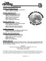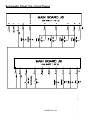
1
UNIVERSAL
AUDIO AMPLIFIER
SYSTEM
Ramsey Electronics Model No.
UAM4SYS
The UAM4SYS is a state of the art audio amplifier that utilizes a class
D power amplifier. Professional balanced input is provided along with
an unbalanced line output that can be configured as a buffered input
feed thru or as the “processed”, (tone, balance, level) signal to feed
remote locations. All controls use DC or digital levels, eliminating
control noise. Headphone level is provided by a 64 step digital
control with memory. Automatic over temperature protection and
power stage mute is provided. All this in a rugged compact
aluminum case.
FEATURES
•
•
•
•
•
•
•
•
•
•
•
•
42 watt class D amplifier (21W per channel stereo mode)
0.1% + N distortion
Balanced or unbalanced inputs
All DC or digital controls for noise free operation
Selectable direct or processed (bass, treble, balance, level, loudness) line
outputs
Pre-mute headphone output
64 step digital headphone level adjustment with level memory
Operates on 12 to 18VDC @ 3.3A max power input (up 87% efficient)
Quick connect spring terminal output terminals accept 28AWG to 14AWG
wire
Selectable 22, 25, 29.5 or 36dB gain
Rugged shielded aluminum case
Compact profile (5.6in x 6.6in x 1.6in) weighs in at 1.24 lbs (excluding
power supply)
UAM4SYS • 1
PARTIAL LIST OF AVAILABLE KITS:
RAMSEY TRANSMITTER KITS
• FM10C, FM25B FM Stereo Transmitters
• AM1C, AM25 Transmitter
RAMSEY RECEIVER KITS
• FR1C FM Broadcast Receiver
• AR1C Aircraft Band Receiver
• AR2 Aircraft Band Receiver
• SR2C Shortwave Receiver
• AA7C Active Antenna
• SC1C Shortwave Converter
RAMSEY HOBBY KITS
• SG7 Personal Speed Radar
• SS70C Speech Scrambler/Descrambler
• TT1CTelephone Recorder
• MD3C Microwave Motion Detector
• PH14C/15C/16C Peak hold Meters
RAMSEY AUDIO KITS
• SHA1C and SHA2 Headphone Amplifier kits
• UAM4 40 Watt Stereo Amplifier kit
RAMSEY AMATEUR RADIO KITS
• HR Series HF All Mode Receivers
• DDF1 Doppler Direction Finder Kit
• QRP Series HF CW Transmitters
• CW7C CW Keyer
• QRP Power Amplifiers
RAMSEY MINI-KITS
Many other kits are available for hobby, school, scouts and just plain FUN! New
kits are always under development. Write, call or visit www.ramseykits.com for
our free Ramsey catalog.
UAM4SYS
Ramsey Electronics publication No. UAM4SYS, Rev. 3.4a
First Printing, October, 2008
This Printing, June, 2010
COPYRIGHT 2008-2010 by Ramsey Electronics, LLC, 590 Fishers Station Drive, Victor, New
York 14564. All rights reserved. No portion of this publication may be copied or duplicated without
the written permission of Ramsey Electronics, LLC. Printed in the United States of America.
UAM4SYS • 2
Ramsey Publication No. UAM4
Manual Price Only $5.00
KIT ASSEMBLY
AND INSTRUCTION MANUAL FOR
Universal Audio
Amplifier System
TABLE OF CONTENTS
Theory of Operation........................................... 4
“Learn-As-You-Build” Kit Assembly.................. 11
Parts List.......................................................... 13
Assembly Steps................................................ 14
Setup and Testing ............................................ 24
Specifications ................................................... 36
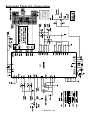
Schematics ..................................................38-41
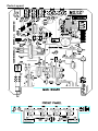
Parts Layout Diagram....................................... 42
Ramsey Kit Warranty........................................ 43
RAMSEY ELECTRONICS, LLC
590 Fishers Station Drive
Victor, New York 14564
Phone (585) 924-4560
Fax (585) 924-4555
www.ramseykits.com
UAM4SYS • 3
UAM4SYS Theory of Operation
Note: There are four pages of schematics included in this manual. Please
refer to them as directed as you read the following.
Power Supply
Since electronic equipment doesn’t work without power, lets start off by
describing the UAM4SYS power supply. For reference when reading this
section, check schematic sheets 1 and 2 (pages 38 & 39). The UAM4SYS
requires a 12 to 18 volt DC input at 3.3 amps applied to Power jack J5. From
there the power goes two directions. First, to VR1, a 7810 positive 10 volt 1
amp regulator. C28 filters the regulator’s output. 10 Volts is used to power
most of the circuitry you see in schematic 1, as well as the 5 volt power
supply on schematic sheet 2. Since the regulator is before the power switch,
all circuits powered by the 10 volt are powered as soon as the unit is plugged
in. On schematic sheet 2, regulator VR2, a 7805 positive 5 volt 1 amp
regulator that powers circuitry on schematic sheets 1, 2, and 4. C39 filters
VR2’s 5 volt output.
Turn back to schematic sheet 1. The second place the input power is routed
to the power switch, S1. When this switch is turned on, power is applied to
the power amp IC, U7 on schematic page 4. It is also applied to R29 through
J6 pin 10 to J40 pin 1 on the front panel (schematic sheet 3). This causes
D4, the power indicator LED, to light.
An interesting note is that because the 10 volt and 5 volt circuits are active
whenever the power supply is plugged in, you can listen to the input signal
on the headphones and the line outputs will be active even though the power
switch is off. The operation of these sections is discussed in detail in the
following sections. I’m sure you can think of some interesting applications for
this ‘feature!’
Input Buffer
IC U1 contains 4 operational amplifiers, (op amp). U1A and U1B are set up
as a buffer with unity gain. C5, C10, C11, and C12 are input coupling
capacitors. They provide DC isolation between the input audio device and
the UAM4SYS. R11 and R14 provide a 5 volt bias to the op amp buffers.
Because the input can be a balanced signal and there is negative feedback
applied to the ‘-‘ input of U1A and U1B, R1, R15, R23 and R24 are
necessary to isolate that feedback signal from the applied input signal. A
resistor is needed on both the ‘+’ and ‘-’ inputs because the signal is
balanced. C47 provides filtering of any signal that might try to sneak thru to
the power supply and therefore assures a stable reference bias on the op
amp input.
UAM4SYS • 4
The input buffer allows both unbalanced and balanced input signals to be
applied to the UAM4SYS. First we will take an unbalanced signal into the
unbalanced input at J4.
An unbalanced single is one that uses two conductors, one for the audio
signal and one for ground. This is the type of signal that comes out of an
MP3 player, CD player, tape deck, VCR, computer, or other similar device.
J4 takes a 3.5mm Stereo plug. A 3.5mm stereo plug consists of three
conductors called tip, ring, and sleeve. The tip at the very end of the plug is
normally the left audio channel. The next conductor down is called the ring
and is normally the right audio channel. The last and biggest conductor is
called the sleeve and is the ground connector that is common to both the left
and right channels.
Now that we know what a 3.5mm stereo plug is lets follow an unbalanced
signal from the connector through the Input Buffer. When a plug is inserted
into J4 the electrical connections between pins 2 & 4 and 1 & 3 are opened.
The left channel signal from the tip enters J4 pin 2 through C10 and R1 to
U1A’s non-inverting input at pin 3. The left channel signal is buffered and
exits at pin1. The right channel signal from the ring enters J4 pin 1 though
C11 and R23 to U1B’s non-inverting input at pin 5. The right channel signal
is buffered and exits at pin 7. Ground comes in on the sleeve and is
connected to the circuit board ground plane.
A little information about balanced signals is probably a good idea at this
time. Balanced audio signals use three conductors, positive, negative, and
ground for each channel. The actual signal is not referenced to ground but is
applied on the ‘+’ and ‘-’ lines. The signal on the ‘+’ line is exactly the
opposite of the ‘-’ line. The two signals are applied to the two amplifier inputs
and the amplifier uses both of these to produce an output. The ground is
simply there to provide some shielding of the cable and is not used in any
other way. Most noise that sneaks onto the lines will be the same level, both
in amplitude and polarity at any given time. Since it is applied to the opposite
polarity inputs the noise will be canceled and not appear at the output. This
is called common mode rejection, a big advantage of the differential inputs of
the op amps. Balanced lines are used in most professional equipment and
for long signal runs.
For separate unbalanced inputs we will again use a 3.5mm stereo plug but
now we need one for each channel. When a plug is inserted into J2 and J3
the electrical connections between pins 2 & 4 and 1 & 3 of these jacks are
opened. Let’s follow the right channel and leave the left channel to you. The
positive tip signal enters J2 pin 4 goes to J4 pin 3 which is connected to pin 1
(no plug in J4). From J4 pin 1 the signal goes through C11 and R23 to U1B’s
non-inverting input at pin 5. The negative ring signal enters through J2 pin 1
UAM4SYS • 5
and goes through C12 and R15 to U1B’s inverting input at pin 6. The right
channel signal is buffered and exits at pin 7.
J2 and J3 can also be used as unbalanced inputs by simply connecting an
unbalanced input to the connector tip and the ground to the ring and sleeve.
The signal will now be applied to the ‘-’ input of the op amps and the op amp
‘+’ inputs will be tied to ground. This is handy if you have inputs that use
separate left and right cables and mono 3.5mm plugs. Also, when using the
UAM4SYS in mono mode only the right channel, J2, input is used for mono
operation. Again this can then be used either balanced or unbalanced.
From the output of the input buffer the left and right audio signals go to two
different places. First they go to the line output buffer input headers H1 and
H2. They also go to the tone, volume, balance control IC, U3.
Tone/Volume/Balance
U3, an LM1034, provides tone, volume, balance, and loudness control for both
channels of the UAM4SYS. The IC supplies a DC reference voltage for the
bass, treble, balance, and volume controls. These controls are adjusted by
the user and provide individual DC levels to the IC where they set appropriate
levels of each function. Because DC levels are used to control the various
functions the scratchy noise produced by the controls in many audio
components is not a problem in the UAM4SYS.
C15 and C21 set the treble operation points. C19 and C20 set the bass
operation points. C18 and C16 are bypass capacitors for the IC. C6, C7, C8,
and C26 act as filters for the DC control lines. R17, R18, R19, and R20 (sheet
3) are the control potentiometers. R5, R6, R8, and R13 provide isolation
between the control pots and the IC. If you wish to learn more about how the
LM1034 actually works and how component values were selected do an
internet search on National Semiconductor and download the data sheet.
The unprocessed audio enters U3 pins 2 and 19 from the input buffers
through C9 and C4 which are coupling capacitors. The audio is then
processed according to the settings of the control potentiometers and fed to
the right channel output at pin 8 and left channel output at pin 13. From here
the processed audio goes three places the line output buffer headers H1 & H2
(sheet 1), headphone amp (sheet 2), and power amp (sheet 4).
Loudness
The loudness function is turned on when U3 pin 7 is connected to U3 pin 12.
It is turned off when U3 pin 7 is connected to U3 pin 17. Loudness is
controlled by front panel switch S4 (sheet 3) which controls U5A and U6 as
described below.
UAM4SYS • 6
U5A is a flip flop set up in the toggle mode. Its outputs at pin 6, called ‘Q’, and
pin 7, called ‘Q not’ indicated by a line over the Q symbol, are opposite DC
levels of either +5 volts or 0 volts. R27 is a pull up resistor for the flip flop’s
set line. C32 delays the +5 volts to U5A’s set line ensuring it comes up in the
set condition, which is +5V on output ‘Q’ at pin 6 and 0V on pin 7, ‘Q not’,
when power is first turned on. When S4 is pressed it applies a ground to C31
(sheet 2) causing C31 to discharge. When the button is released the ground
is removed from C31 and it charges through R38 to +5 volts. This positive
transition causes U5A to change states, (flip flop). An interesting thing to
know is when a switch opens or closes it usually has problems and may
actually open and close many times before finally ending up in it’s final state.
This is called switch bounce and is actually ‘seen’ by logic circuits like U5 and
causes unpredictable results. C31 and R38 help prevent these ‘bounces’ from
getting to U5 and is called de-bouncing.
U6 is called an analog switch. It contains 4 electronic switches, we’ll only be
using 2 of them that are turned on and off by signals applied to pins 7 and 13.
With +5 volts on these pins it’s associated switch is turned on and 0 volts
turns it off. With U5 Pin 6 at +5 volts U6 pin 13 is also at +5 volts. This
causes the switch between U6 pins 1 and 2 to close. At the same time U5 pin
7 is at 0V. This applies 0V to U6 pin 5 which causes the switch between U6
pin 3 and 4 to open. This turns off the Loudness function as mentioned
above. When S4 is pressed and released, U5A toggles causing pin 6 to
change to 0V and pin 7 to change to +5V. This places 0V on U6 pin 13
opening the switch between pins 1 and 2. It also places +5 V on U6 pin 5
closing the switch between pins 3 and 4 and turns off the loudness function.
Since pin 7 is +5V, power is applied to the loudness LED on the front panel
(sheet 3) through current limiting resistor R28 which lights the LED indicating
the UAM4SYS is muted.
Line Output Buffer
With headers H1 and H2 the user can select either processed (from U3) or
unprocessed (directly from input buffers U1A and U1B) audio to be sent to the
line outputs. R4 and R30 set the bias to ½ supply voltage (+5 volts) while
isolating the bias voltage from the power supply. R32 and R33 are pull-up
resistors which prevent oscillations that can be caused by external load
capacitance. C13, C14, C17, and C30 are coupling capacitors. The selected
right channel audio signal enters through the header pin 2 and is applied to
the op amp buffer through C14. The output at U1 pin 8 is applied to the right
line output RCA connector through C17. The left channel is identical to the
right.
Notice that the signal to the line output buffer is before the mute function
which will be discussed in the ‘Power Amp’ description. This means that even
though the amplifier is muted the input signal will be present on the line output
UAM4SYS • 7
jacks. Therefore if you are using the line outputs to record a program you can
mute the speakers but continue to record the input. If you are feeding another
amplifier the mute function on the UAM4SYS will silence only the local
amplifier output.
Headphone Amplifier
U11 and U12 (sheet 2) are 750mW headphone amplifiers. C45 is a power
supply filter capacitor. C33, C37, C34, and C38 are coupling capacitors. C35
and C36 are bypass capacitors. U10 is a digital potentiometer that provides a
DC level output at pin 6 that controls the gain of U11 and U12. S5 and S6
(sheet 3) are used to increase or decrease this DC level.
To increase the gain of the headphone amps S6 is pressed. This places a
ground on pin 2 of U10. This high to low transition tells the IC to increase the
output voltage (pin 6) 1/64 of the +V to –V voltage (5 volts). If S6 is held down
for more that one second the output voltage will go another 1/64 step every
100 milliseconds until it is released or the full +5 volt level is reached. The
output voltage is applied to the volume control, pin 4, of U11 and U12. The
down button S5 functions just like S6 except the voltage is decreased. The
really neat thing about U10 is that it remembers where it is set even when the
power is removed. So if you turn off the UAM4SYS and then turn it back on
the headphone level will be where you left it. Also notice that the signal to the
headphones is before the mute function, just like the line output signals, which
will be discussed in the ‘Power Amp’ description. This means that even
though the amplifier is muted you can still hear the input signal. Therefore you
can make sure the correct program is ready to go before you apply it to the
speakers for everybody else to hear.
The right channel audio from the Tone/Volume/Balance IC, U3, is applied to
U12 through C38. The signal is amplified and fed to headphone jack J20
through C34.
Power Amp
The Power Amp U7 a MAX9708, is a class D amplifier. The letter D is simply
the next letter after C, and does not stand for digital. Class D and Class E
amplifiers are sometimes mistakenly described as "digital" because the output
waveform superficially resembles the pulse-train of a digital signal, but a Class
D amplifier merely converts an input waveform into a continuously pulse-width
modulated (square wave) signal. A digital waveform would be pulse-code
modulated.
Class D amplifiers are much more efficient than Class AB power amplifiers. As
such, Class D amplifiers do not need large transformers and heavy heat sinks,
which mean that they are smaller and lighter in weight than an equivalent
UAM4SYS • 8
Class AB amplifier. All power devices in a Class D amplifier are operated in
on/off mode. The term usually applies to devices intended to reproduce
signals with a bandwidth well below the pulse switching frequency which in
our case is about 200kHz.
The MAX9708 converts the input signal to a sequence of pulses whose
averaged value is directly proportional to the instantaneous amplitude of the
signal. The frequency of the pulses is typically ten or more times the highest
frequency of interest in the input signal. The pulse frequency in the Power
Amp is around 200kHz or 10 times 20kHz. The output of such an amplifier
contains unwanted spectral components (that is, the pulse frequency and its
harmonics) which must be removed by a passive filter. The resulting filtered
signal is then an amplified replica of the input. This filtering is handled by the
patented technology of the Maxim MAX9807 amplifier chip and the speaker.
The design uses a unique filterless modulation and spread-spectrum switching
mode. This eliminates the need for large inductors and capacitors on the
output.
Typical class D amplifiers use a simple modulation method called ‘FixedFrequency Modulation’ (FFM). This simply means that a switching frequency
is selected and that is the frequency at which the output is switched. The
MAX9708 can use this method but it also has a special method called
‘Spread-Spectrum Modulation’ (SSM). With this method the switching
frequency is actually changed around a center frequency, in this case +- 4%
around 200kHz. Using this method the MAX9708 is able to reduce the noise
generated with typical class D amplifiers and the need for large filters
described above is minimized. How this is accomplished is beyond this
manual. If you are interested you can find information on the web by
searching for ‘spread spectrum’ and also check out the Maxim web site at
“www.maxim-ic.com” and go to the data sheet for the MAX9708.
The main advantage of a class D amplifier is power efficiency. Because the
output pulses have a fixed amplitude the output devices, which are MOSFETS
in the case of the MAX9708, are switched either on or off rather than operated
in linear mode. This means that very little power is dissipated by the
transistors except during the very short interval between the on and off states.
The MAX9708 is capable of achieving up to 87% efficiency. The wasted
power, the remaining 13%, is low because the instantaneous power dissipated
in the transistor is the product of voltage and current, and one or the other is
almost always close to zero. The lower losses permit the use of a smaller heat
sink while the power supply requirements are lessened too.
The input signal(s) are applied to U7 though C57 and C59. Once the signal
reaches the MAX9708 there isn’t a lot more to say other than it amplifies the
signal and applies it to the output terminals at T1.
SETUP AN
UAM4SYS • 9
The ‘GAIN’ jumpers, H4 and H5, are used to adjust the gain of the MAX9708.
See the tables on the schematic for specific settings. The gain settings are
also printed on the UAM4SYS circuit board next to the jumpers.
The ‘MUTE’ input terminal located below the left and right channel inputs is
used to place the UAM4SYSinto the mute mode. The mute mode causes the
output transistors to stop switching. This may be used to silence the
UAM4SYS with the advantage of a built in click/pop suppression feature of the
MAX9708. Shutdown mode reduces the power consumption of the
UAM4SYS to a very low level, about 0.1uA. This is handy for battery operated
applications to increase battery life. The mute function is controlled by the
second half of flip flop IC U5. This circuit operates in exactly like the flip flop
used for the loudness function with the exception that the ‘Q’ output on pin 10
is connected to the power amplifier, U7 pin 31, instead of controlling an analog
switch. U7 is muted when the ‘Q’ output is low, 0 volts. Note that the mute
function only controls the output of the speaker output. It will not have any
effect on the headphone or line outputs of the UAM4.
The UAM4SYS may be operated as either a 2 channel, 21 watt per channel,
or a single 42 watt amplifier. The mode of operation is determined by header
jumper H3 and the placement of jumpers at L+, L-, R+ & R- located near the
output terminals. With no jumper installed on H3 the MAX9708 is in 2 channel
or stereo mode. This means that it is operating like two separate amplifiers.
In this mode there should be no jumpers installed at the L+, L-, R+, & Rpoints.
DO NOT INSTALL ANY JUMPERS AT L+, L-, R+, & R- WHEN NO JUMPER
IS INSTALLED AT H3
If a jumper is installed at H3 the MAX9708 will operate in mono mode. In this
mode only the signal applied to the right channel input is used. You may use
the UAM4SYS as either a single 42 watt amplifier if are installed between L+
& R+ and between L+ & R-. If jumpers are not installed between L+ & R+,
and between L+ & R-, the UAM4SYS will operate as two 21 amplifiers with the
same input signal.
Note that even though it appears you could connect the left and right speaker
outputs together at a point away from the UAM4SYS
DO NOT ATTEMPT THIS!!!
Connections away from the board may cause signal phasing differences and cause
damage to your UAM4SYS.
UAM4SYS • 10
That’s about it. The rest of the components are simply support components
required by the MAX9708 and are used to provide stable voltages and signals
generated within the MAX9708. Again if you want more in depth information
about the MAX9708 go to “www.maxim-ic.com” and locate the data sheet for
it.
RAMSEY Learn-As-You-Build KIT ASSEMBLY
Successful kit assembly requires close attention to the assembly the assembly
instructions, good soldering techniques and proper tools. Here are some
helpful suggestions.
•
•
•
•
•
Use a 25-watt soldering pencil with a clean, sharp tip.
Use only rosin-core solder intended for electronics use.
Use bright lighting; a magnifying lamp or bench-style magnifier may
be helpful.
Do your work in stages, taking breaks to check your work. Carefully
brush away wire cuttings so they don't lodge between solder
connections.
We have a two-fold "strategy" for the order of the following kit assembly steps.
First, we install parts in physical relationship to each other, so there's minimal
chance of inserting wires into wrong holes. Second, whenever possible, we
install in an order that fits our "Learn-As-You Build" Kit building philosophy.
This entails describing the circuit that you are building instead of just blindly
installing components. We hope that this will not only make assembly of our
kits easier, but help you to understand the circuit you’re constructing. For
each part, our word "Install" always means these steps:
1. Pick the correct part value to start with.
2. Place it in the correct PC board location.
3. Orient it correctly, follow the PC board drawing and the written
directions for all parts - especially when there's a right way
and a wrong way to place it on the board. (Diode bands, electrolytic
capacitor polarity, transistor shapes, dotted or notched ends
of IC's, and so forth.)
4. Solder all connections unless directed otherwise. Use enough heat
and solder flow for clean, shiny, completed connections.
UAM4SYS • 11
SURFACE MOUNT COMPONENT SOLDERING INSTRUCTIONS:
You’ll notice that the circuit board contains only a few holes for component
leads to pass through. This is because the SMT components will be affixed to
the TOP side of the PC board, the side with the white printing. Be aware that
the component view for assembly is looking at the TOP side of the PC board.
Patience is the key when installing surface mount components. Typically, the
first step (after identifying the component) is to “tin” one of the PC traces that
will connect to the part. Once this is accomplished, the part can be installed by
holding it with tweezers in contact with the “tinned” trace and re-heating the
solder (see the following diagrams). Another commonly used technique is to
glue the surface mount components to the printed circuit board before
soldering. The procedure is to take a small amount of glue (usually with a pin
or toothpick) and “dab” the circuit board in the place where the component will
be affixed. Be careful not to apply too much glue as when the part is placed it
may “squash” the glue underneath the soldering tabs of the component.
Carefully place the part into position, and when the glue dries, solder the
connection.
UAM4SYS • 12
UAM4SYS PARTS LIST
Sort and “check off” the components in the boxes provided. We do our best to
pack all our kits correctly but it is possible that a mistake has occurred and we
missed a part. Please note that physical descriptions of parts are for those
currently being shipped. Sometimes the parts in your kit may have a different
appearance but still have the same values. Do not separate Surface Mount
parts from their packaging until installation.
CAPACITORS
3 0.01uF Ceramic Disk [marked 103] (C3, 15, 21)
8 0.1uF Ceramic Disk [marked 104] (C24, 31, 40, 41, 42, 44, 46, 47)
8 0.22uF Ceramic [marked 224] (C6, 7, 8, 23, 26, 32, 37, 38)
2 0.39uF Metal Film [marked 394] (C19, 20)
2 1uF Electrolytic [marked 1uF] (C35, 36)
18 10uF Electrolytic [marked 10uF] (C4, 5, 9, 10, 11, 12, 13, 14, 16, 17,
18, 22, 28, 29, 30, 39, 45) {extra included to make test jig}
2 100uF Electrolytic [marked 100uF] (C33, 34)
1 1000uF 25Volt Electrolytic [marked 1000uF 25V] (C1)
4 47uF Tantalum SMT [marked 476] (C48, 50, 60, 62)
Preinstalled
1 0.01uF Ceramic 0805 SMT [not marked] (C53) Preinstalled
4 0.1uF Ceramic 0805 SMT [not marked] (C49, 51, 55, 61) Preinstalled
4 0.001uF Ceramic 0805 SMT [not marked] (C25, 27, 43, 63)
Preinstalled
5 1uF Ceramic 0805 SMT [not marked] (C54, 56, 57, 58, 59)
Preinstalled
1 4.7uF tantalum 1210 SMT [not marked] (C52) Preinstalled
RESISTORS
2 150 ohms [marked Brown, Green, Brown] (R34, 35)
2 1 K ohms [marked Brown, Black, Red] (R32, 33)
7 2.2 K ohms [marked Red, Red, Red] (R21, 22, 27, 28, 29, 37, 38)
4 10 K ohms [marked Brown, Black, Orange] (R1, 15, 23, 24)
4 47 K ohms [marked Yellow, Violet, Orange] (R5, 6, 8, 13)
2 470 K ohms [marked Yellow, Violet, Yellow] (R11, 14)
2 1M ohm [marked Brown, Black, Green] (R4, R30)
4 10 K ohms Potentiometer [marked B10K] (R17, 18, 19, 20)
1 4.7 K ohms SMT 0805 [marked 472] (R2) Preinstalled
1 2.2 K ohms SMT 0805 [marked 222] (R7) Preinstalled
2 10 K ohms SMT 0805 [marked 103] (R3, 9) Preinstalled
SEMICONDUCTORS
4 LED [red] (D1, 3, 4, 5)
1 LMC660AIN [marked LMC660AIN] (U1)
1 LM1036N [marked LM1036N] (U3)
UAM4SYS • 13
1
1
1
1
1
1
2
1
74HC109 [marked 74HC109] (U5)
CD4066DCN [marked CD4066] (U6)
DS1669 [marked DS1669] (U10)
7810 [marked 7810] (VR1)
7805 [marked 7805] (VR2)
MMBT3906 [marked 2A] (Q3) Preinstalled
LM4875M [marked LM4875M] (U11, 12) Preinstalled
MAX9708 [marked MAX9708] (U7) Preinstalled
MISCELLANEOUS
4 3 Pin Header (H1, 2, 4, 5)
1 2 Pin Header (H3)
2 RCA Jack (J1, 8)
4 3.5 mm Phone Jack (J2, 3, 4, 20)
1 2.1 mm Power Jack (J5)
2 10 Pin Dual In-Line Connector (J40, J7)
1 DPDT Push Button Switch (S1)
4 SPST Momentary Push Button Switch (S2, 4, 5, 6)
1 4 Pin Wire Locking Connector (T1)
5 Jumper Blocks
1 5” length of 18 gauge wire.
4 Ferrite bead filter SMT 805, 600 ohms@100MHz(L1, 2, 3, 4)
Preinstalled
HARDWARE
6 Beryllium Grounding Fingers
1 Push Button Cover
4 Knobs.
ASSEMBLY
We will begin with the main board oriented in the direction shown. Be sure not
to confuse the side of the board where the parts go. On the board you will see
the side that has white silk screen parts locations. This is the side where most
parts are mounted. We will begin with lower profile parts and work up to the
higher ones in each functional section. Don’t use sockets for integrated
circuits (IC’s).
In this day of miniaturization not all parts are made in the familiar through-hole
style packages (a part with leads that go through the circuit board and are
soldered on the board’s back side). Some of these parts come in surface
mount or SMT packages (parts that are soldered on the same side of the
circuit board they mount on). An example of this is the MAX9708 Class D 40
watt audio amplifier IC (U7) used in this kit. Since SMT parts are normally
small they can be difficult or impossible to install by hand, so we have installed
UAM4SYS • 14
them and the circuit has been pre-tested at the factory for you. Due to circuit
requirements U7’s support parts are also SMT.
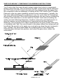
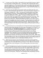
GF. GROUNDING FINGER INSTALLATION
I know you are anxious to start soldering parts but first let’s install the
beryllium grounding fingers in the case bottom. These fingers have glue that
needs to set before the circuit board can be installed in the case. Let’s use
our time efficiently by using the time we are going to take installing parts to
also let the glue set on the fingers.
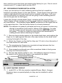
Locate the 6 brass colored shield ‘finger’ contacts and the case bottom.
These fingers will be mounted on the two small ’shelves’ along the edges of
the case bottom. The shielding fingers MUST be placed so the fingers are all
in the same direction. See the picture below for correct placement.
NOTE: The adhesive is pressure activated and once you press it in place any
attempt to reposition it will result in failure of the adhesive, so make
sure the fingers are all facing the same direction BEFORE pressing
into place! It is best to clean the case bottom with denatured or
rubbing alcohol before attaching the fingers.
1. Remove the protective paper on the double back tape, and position the
finger so it is tight against the side of the case bottom on the small ’shelf’
running the length of the tray.
2. Mount four fingers on the shelf so they are 1/2 inch in from the ends of
the case bottom on each side.
3. The remaining two fingers are mounted mid way between the four
fingers installed in the previous step.
4. Once properly positioned use a flat screwdriver blade to firmly press
the strip onto the case bottom.
5. Set the case bottom aside for now. Full adhesion requires 24 hours.
Be careful not to disturb the fingers once pressed into place.
MOUNTING TAPE
BACK
SLIDE BOARD IN
IB. INPUT BUFFER CIRCUIT
1. Install R15, a 10K ohm resistor (marked Brown, Black, Orange).
Resistors have no special polarity so they can be installed in either
direction.
UAM4SYS • 15
2. Install R23, another 10K ohm resistor (marked Brown, Black, Orange).
3. Install R1, yet another 10K ohm resistor (marked Brown, Black,
Orange).
4. Install R24, the last 10K ohm resistor (marked Brown, Black, Orange).
5. Install R11, a 470K ohm resistor (marked Yellow, Violet, Yellow).
6. Install R14, the last 470K ohm resistor (marked Yellow, Violet, Yellow).
7. Install U1, the LMC660AIN quad operational amplifier IC (marked
LMC660AIN). Before soldering make absolutely sure that you have
installed all 14 pins through the appropriate holes. Verify that the notch or
dot indicating pin one is facing the same direction shown in the parts
layout diagram or the circuit board’s silk screen. Solder two pins in
opposite corners of the IC. Make sure the IC is flat and square to the
board. If not, reheat one pin at a time to properly seat the IC. Now solder
the rest of the pins. Check for any possible solder bridges when you’re
done.
8. Install C47, a 0.1uF ceramic capacitor (marked 104). Ceramic
capacitors are like resistors they have no polarity so they can be installed
in either direction.
9. Install C12, a 10uF electrolytic capacitor (marked 10uF). This is the
first electrolytic capacitor you are about to install. Pay close attention to
the polarity markings on this part and all subsequent electrolytic
capacitors. In most cases the negative (-) side is marked on the capacitor,
while the positive side (+) is marked on the parts layout. If you fail to
mount this component correctly, the part can fail as well as prevent proper
operation of your project. Maker sure you install the (+) lead of the
capacitor in the (+) lead of the board. We will be installing many more of
these later in the project so be sure and remember this!
10. Install C11, another 10uF electrolytic capacitor (marked 10uF).
Watch that polarity!
11. Install C10, another 10uF electrolytic capacitor (marked 10uF).
Polarity check!
12. Install C5, yet another 10uF electrolytic capacitor (marked 10uF).
Four in a row, I probably don’t have to remind you about that polarity thing
again.
13. Install J2, a 3.5mm stereo phone jack. Make sure that this jack and
all that follow in this kit sit flat and square to the board before soldering.
14. Install J4, another 3.5mm stereo phone jack.
UAM4SYS • 16
15. Install J3, the last 3.5mm stereo phone jack in this section.
LOB. LINE OUTPUT BUFFER CIRCUIT
1. Install R33, a 1K ohm resistor (marked Brown, Black, Red).
2. Install R32, another 1K ohm resistor (marked Brown, Black, Red).
3. Install R4, a 1M ohm resistor (marked Brown, Black, Green).
4. Install R30, the last 1M ohm resistor (marked Brown, Black, Green).
5. Install C46, a 0.1uF ceramic capacitor (marked 104).
6. Install H1 a 3 pin header. Solder one pin first, make sure the header is
flush and square to the board before soldering the last two pins.
7. Install H2 another 3 pin header. Install this part just like H1.
8. Install C14, a 10uF electrolytic capacitor (marked 10uF). Remember to
watch polarity!
9. Install C13, yet one more 10uF electrolytic capacitor (marked 10uF).
10. Install C17, another 10uF electrolytic capacitor (marked 10uF).
11. Install C30, the last 10uF electrolytic capacitor in this section (marked
10uF).
12. Install J8, an RCA jack. Make sure this jack is flush and square
before soldering.
13. Install J1, another RCA jack. Installed just like J8.
TVB. TONE/VOLUME/BALANCE CIRCUIT
1. Install R5, a 47K ohm resistor (marked Yellow, Violet, Orange).
2. Install R8, another 47K ohm resistor (marked Yellow, Violet, Orange).
3. Install R6, that’s right another 47K ohm resistor (marked Yellow, Violet,
Orange).
4. Install R13, the last 47K ohm resistor (marked Yellow, Violet, Orange).
5. Install U3, a LM1036N tone control IC (marked LM1036N). Before
soldering make absolutely sure that you have installed all 20 pins through
the appropriate holes. Verify that the notch or dot indicating pin one is
facing the same direction shown in the parts layout diagram or the circuit
board’s silk screen. Solder two pins in opposite corners of the IC. Make
sure the IC is flat and square to the board. If not, reheat one pin at a time
UAM4SYS • 17
to properly seat the IC. Now solder the rest of the pins. Check for any
solder bridges when you’re done.
6. Install C26, a 0.22uF ceramic capacitor (marked 224).
7. Install C3, a 0.01uF ceramic capacitor (marked 103).
8. Install C7, a 0.22uF ceramic capacitor (marked 224).
9. Install C19, a 0.39uF metal film capacitor (marked 394). Metal film
capacitors are like ceramic capacitors, they have no polarity.
10. Install C21, a 0.01uF ceramic capacitor (marked 103).
11. Install C15, the last 0.01uF ceramic capacitor (marked 103).
12. Install C6, a 0.22uF ceramic capacitor (marked 224).
13. Install C20, a 0.39uF metal film capacitor (marked 394).
14. Install C8, a 0.22uF ceramic capacitor (marked 224).
15. Install C16, a 10uF electrolytic capacitor (marked 10uF). Remember
to check polarity.
16. Install C4, another 10uF electrolytic capacitor (marked 10uF).
17. Install C22, you guessed it another 10uF electrolytic capacitor
(marked 10uF).
18. Install C9, yet another 10uF electrolytic capacitor (marked 10uF).
19. Install C18, the last 10uF electrolytic capacitor it this circuit (marked
10uF).
HA. HEADPHONE AMPLIFER CIRCUIT
We have preinstalled the surface mount (SMT) IC’s U11 and U12 for you.
1. Install R34, a 150 ohm resistor (marked Brown, Green, Brown).
2. Install R35, another 150 ohm resistor (marked Brown, Green, Brown).
3. Install U10, a DS1669 digital rheostat IC (marked DS1669). Install this
IC like you did U1 and U3.
4. Install C38, a 0.22uF ceramic capacitor (marked 224).
5. Install C37, another 0.22uF ceramic capacitor (marked 224).
6. Install C45, a 10uF electrolytic capacitor (marked 10uF). Very good
UAM4SYS • 18
you remembered to check polarity!
7. Install C35, a 1uF electrolytic capacitor (marked 1uF).
8. Install C36, the last 1uF electrolytic capacitor it this circuit (marked
1uF).
9. Install C33, a 100uF electrolytic capacitor (marked 100uF).
10. Install C34, the last 100uF electrolytic capacitor it this circuit (marked
100uF).
11. Install J20, the last 3.5mm stereo phone jack.
M. MUTE CIRCUIT
1. Install R22, a 2.2K ohm resistor (marked Red, Red, Red).
2. Install R21, another 2.2K ohm resistor (marked Red, Red, Red).
3. Install R37, the last 2.2K ohm resistor in this circuit (marked Red, Red,
Red).
4. Install U5, a 74HC109 dual JK flip-flop IC (marked 74HC109). Install
this IC like you did U1, U3, and U10.
5. Install C24, a 0.1uF ceramic capacitor (marked 104).
6. Install C23, a 0.22uF ceramic capacitor (marked 224).
7. Install C44, the last 0.1uF ceramic capacitor in this circuit (marked
104).
L. LOUDNESS CIRCUIT
1. Install R27, a 2.2K ohm resistor (marked Red, Red, Red).
2. Install R38, another 2.2K ohm resistor (marked Red, Red, Red).
3. Install R28, the last 2.2K ohm resistor in this circuit (marked Red, Red,
Red).
4. Install U6, a CD4066 analog switch IC (marked CD4066). Install this
like you did the other IC’s.
5. Install C41, a 0.1uF ceramic capacitor (marked 104).
6. Install C31, another 0.1uF ceramic capacitor (marked 104).
7. Install C32, the last 0.22uF ceramic capacitor (marked 224).
UAM4SYS • 19
8. Install C42, a 0.1uF ceramic capacitor (marked 104).
PS. POWER SUPPLY CIRCUIT
1. Install R29, the last 2.2K ohm resistor (marked Red, Red, Red).
2. Install C28, a 10uF electrolytic capacitor (marked 10uF). That’s right,
watch the polarity. You are getting good at this.
3. Install J5, the 2.1mm power jack. Make sure it is flush and square to
the board before soldering.
4. Install S1, a DPST power switch. Just like with the jacks, make sure
this part is flush and square to the circuit board before soldering.
5. Install VR1, a 7810 +10 volt regulator. This part is polarity sensitive so
it must go into the board in a certain way. Take a close look at VR1’s
pattern on the layout diagram or the circuit board’s silk screen. It is made
up of two rectangles. The smaller rectangle represents the metal tab on
the actual regulator. Install VR1 so the metal tab faces C28.
6. Install C40, the last 0.1uF ceramic capacitor (marked 104).
7. Install C39, a 10uF electrolytic capacitor (marked 10uF). Polarity!
8. Install C29, finally the last 10uF electrolytic capacitor (marked 10uF).
9. Install VR2, a 7805 +5 volt regulator. VR2 is like VR1 every way
except output voltage. Install VR2 so the metal tab faces C45.
A. AMPLIFIER CIRCUIT
Most of the parts in the amplifier circuit are surface mount or SMT. Since
some of these parts are almost impossible to install by hand they have been
installed for you.
1. Install H3 a 2 pin header. Solder one pin first, make sure the header is
flush and square to the board before soldering the other pin.
2. Install H4 a 3 pin header. Solder one pin first, make sure the header is
flush and square to the board before soldering the last two pins
3. Install H5 the last 3 pin header. Install this part just like H4.
4. Install T1 a 4 position spring loaded terminal block. This part must be
flush and square to the board before soldering.
5. Install C1, a 1000uF electrolytic capacitor. Remember to watch
polarity!
UAM4SYS • 20
6. Find the 5” length of 18 gauge wire. Strip ¼ inch of the insulation from
each end. Twist the little wires together and lightly tin each end. Solder
one end of the wire in the hole at JP2.
7. Route the wire below C37, C9, C22, and C4 and continue on above
C16 and straight down to JP1 just above power switch S1.
8. Solder this end of the wire in the hole at JP1.
FPB. FRONT PANEL CIRCUIT BOARD
It is time to assemble the front panel. DO NOT install D1, D3, D4, and D5
until told to do so in the “Board Attachment” section. We need to get the
proper spacing for these LED’s so they fit properly through the front panel.
1. Install S2, a SPST momentary push button switch. This switch looks
square but it is not. It will only go into the circuit board two ways, either
way will work.
2. Install S4, another SPST momentary push button switch.
3. Install S5, a third SPST momentary push button switch.
4. Install S6, the last SPST momentary push button switch.
5. Install R18 a 10K ohm potentiometer. Make sure this part is flush and
square to the circuit board before soldering.
6. Install R17 a second 10K ohm potentiometer.
7. Install R19 another 10K ohm potentiometer.
8. Install R20 the last 10K ohm potentiometer.
9. Locate one of the 10 pin dual in-line connectors. This part is installed
on the back side and of the circuit board. Find the location for J40 on the
front panel circuit board. Insert the shorter legs of the connector though
from the back side of the circuit board. Make sure this part is flush and
square to the board. Solder the pins on the component or silk screen side
of the circuit board.
10. Install J7, the other 10 pin dual in-line connector, the same way you
installed J40 in the previous step.
BA. BOARD ATTACHMENT
In order to properly attach the front panel circuit board to the main board part
of the case needs to be assembled.
UAM4SYS • 21
1. Locate one of the bezels. (the bezel is the black plastic piece in which
the front panel or back panel sits). The bezel has a smooth side and a
side with ridges on it. The smooth side is where you place the front panel
and the ridged side fits onto the case bottom. The ridges help align the
bezel and panel. Place the front panel into the bezel so that the bezel can
be screwed to the case bottom.
2. Now the front panel/bezel assembly will be mounted onto the case
bottom. Remember that case bottom? We put the beryllium fingers on it
way back in steps GF1- GF6. You must first identify which end of the
case bottom is the front. Notice that the fingers installed in step GF1 –
GF6 are flexible and folded. The BACK of the case bottom is the end
toward the adhesive on the fingers. (See picture after step GF6.) The
front is the other end where the front panel/bezel is to be mounted. We
will use the front panel/bezel assembly from step BA1, and the case
bottom from step GF6. Before assembling the parts you’ll want to peel
the protective plastic from the front panel. The front panel sits inside the
bezel; the included black screws go first though the front panel then the
bezel holding the assembly to the case bottom. Align the holes of the
front panel, bezel, and case bottom front (upper slot) and insert the black
screws.
3. It is now time put our front panel circuit board and main board together.
Slide the main board between the two rows of long pins on J40 and J7 on
the front panel circuit board so that J6 and J9, respectively, on the main
board are aligned. DO NOT SOLDER the connectors at this time.
Now it is time to align the front panel controls with the front panel.
Carefully slide the front panel circuit board and main circuit board
assembly, from step BA3, into the front panel/case bottom assembly from
step BA2. Line up the front panel circuit board so the switches and
potentiometers extend out through the front panel of the case. Make sure
the front edges of the main circuit board are seated firmly against the back
side of the front panel. This is important because it will not be possible to
install the rear panel if there is any space between the two.
4. Slide the front panel circuit board back and forth until all switches,
buttons and the 3.5mm jack are centered in the front panel holes. When
everything is neat and right where you want it to be, take your soldering
iron and solder one of the pins of J9 on the top side of the main circuit
board.
5. Check the alignment one more time because once you make the next
solder connection it will be difficult to take the boards apart. Make sure
the front panel circuit board is square and not angled with respect to the
main board and parallel with the front panel. Make sure that the main
circuit board front left and right tips (under S1 and J20) touch the back
side of the front panel. When you are satisfied that everything is correct
UAM4SYS • 22
solder a pin on J6 on the top side of the main circuit board to hold things
in place.
6. Carefully slide the circuit board assembly out of the case bottom.
Solder the rest of the pins on J6 and J9 on both the top and bottom of the
main circuit board.
7. Insert D1, D3, D4, and D5; red LED’s into the front panel circuit board.
LED’s are polarity sensitive and MUST be installed in the proper direction.
The LED patterns on the layout diagram and the front panel circuit board’s
silk screen show a circle with a flat edge near one of the lead holes. This
flat edge corresponds to a flat edge on the LED. This represents the
cathode lead. Make sure to match the flat edge of the LED to the flat
edge of the board’s silk screen. DO NOT SOLDER the LED’s at this time.
8. Carefully slide the front and main circuit board assembly back into the
front panel/case assembly. Line up the LED’s with their corresponding
hole in the front panel of the case. Make sure that main circuit board front
left and right tips touch the Front Panel of the case. Adjust the LED’s so
that they are all penetrating the front panel equally. It is up to you how far
you wish them to stick out. Solder one lead on each LED. Make sure you
are happy with their alignment and then solder the other lead of each
KLED. Now cut off the excess lead length close to the circuit board.
Verify no solder bridges are across their leads.
AR. ASSEMBLY REVIEW
Before applying power it is a good idea to look over the board for assembly
mistakes. I know you think you were careful during assembly and didn’t make
any mistakes. However, we have noticed that the more confident someone is
that they didn’t make any mistakes, the more likely it is that they did. Over
95% of all kits returned for repair have assembly errors.
The following steps check for common assembly errors that could cause
damage when the kit is powered up. All these steps should be
compared to the parts location diagram. Take your time and examine
the boards carefully.
1. Look over all IC’s for proper orientation.
2. Check all electrolytic capacitors for proper orientation.
3. Check the two regulators VR1 and VR2 for proper orientation.
4. Look between the circuit board and case bottom to make sure all leads
are short enough so they don’t touch the case bottom.
5. Check the back of the front panel circuit board for solder bridges.
UAM4SYS • 23
6. Remove the main/front panel circuit board assembly from the case
bottom and check the back of the main circuit board for solder bridges.
7. Reinstall the circuit boards assemble into the case bottom.
UAM4SYS SET-UP AND TESTING
REQUIRED EQUIPMENT
12 to 18 Volt Power Supply with a 2.1mm power plug (+) center pin
Headphones with a 3.5mm Stereo Phone plug
Unbalanced stereo audio source with 3.5mm Stereo Phone plug (typical
consumer audio outputs such as IPODs, portable CD players, and
computers), unbalanced stereo audio source with two mono plugs (one
left, one right), or Stereo Balanced Audio Source (professional audio) with
two 3.5mm Stereo Phone plugs (one left, one Right)
Two speakers that can handle 20 Watts each
Volt meter
Two, Alligator clip leads
10uF electrolytic capacitor
JUMPER SETTINGS
1. Set the jumpers on headers H1 (REC LEFT) and H2 (REC RIGHT). If you
wish the LINE OUT audio (jacks J1 and J8) to be the same as the input
audio, place the jumpers on both H1 and H2 so that they connect pins 1
and 2 of the headers. If you wish the LINE OUT audio to be processed
by the Tone/Volume/Balance IC then set the jumpers on headers H1 and
H2 so that pins 2 and 3. Set these jumpers to pins 1 to 2 for testing.
2. Set the MONO jumper on H3. If you wish your UAM4SYS to operate in
stereo mode place the jumper on only one pin of H3. This is just to keep
the jumper with the kit so in case you need it in the future you will have it.
For mono mode place a jumper across both pins of H3. For testing set
the unit to stereo mode.
3. Set the GAIN jumpers on H4 and H5. Use the following chart or the one
on the circuit board to set these jumpers. For testing set both jumpers to
pins 1-2.
UAM4SYS • 24
GAIN
H4
H5
+22dB
1-2
2-3
+25dB
2-3
2-3
+29.5 dB
2-3
1-2
+36dB
1-2
1-2
SET-UP
Connect headphones to J20.
Connect a stereo audio source in one of the three configurations below:
Unbalanced audio (3.5mm stereo plug)
Connect an unbalanced audio source to J4.
Unbalanced audio (two 3.5mm mono plugs required for stereo)
Connect the left channel plug to J3.
Connect the right channel plug to J2.
3.5mm stereo plugs can be substituted by making both the
ring and sleeve ground.
Balanced audio (two 3.5mm stereo plugs required for stereo)
Connect the left channel plug to J3.
Connect the right channel plug to J2.
If you are making your own cables, refer to the information below for details on
the different tip-ring-sleeve configurations:
1. Sleeve: usually ground
2. Ring: Right-hand
channel for stereo signals,
negative phase for
balanced mono signals.
3. Tip: Left-hand channel
for stereo signals, positive
phase for balanced mono
signals, signal line for
unbalanced mono signals
4. Insulating rings
Tip-Ring-Sleeve Jack Plug
UAM4SYS • 25
Unbalanced
Balanced
Stereo
Tip
Signal
Positive
Left
Ring
Ground/No Conn.
Negative
Right
Ground
Ground
Ground
Sleeve
Connect speakers to T1. As you look at the back of the unit the left most
contact of T1 is Left (+), the second contact is Left (-), the third contact is
Right (+), and the right most contact is Right (-). Make sure to match these
polarities to your speakers. DO NOT for any reason short the speak wires. If
you are going to use your UAM4SYS in single channel mono mode, connect
the output lines together on the circuit board at the locations provided near T1.
Instructions are provided both on the circuit board and in this manual. It is
recommended that all testing be done in stereo mode so if a problem exists it
is easier to identify.
Set the bass, treble and balance to midrange, volume control fully counter
clockwise and the power switch S1 to off (out position).
TESTING
If any of the following steps fail to produce the indicated result please refer to
the troubleshooting section of this manual.
Power Supply
Note in the following steps all VOLTAGE measurements are take with the
RED or “+” lead of the voltmeter connected to the indicated test point. The
BLACK lead or the terminal labeled “-“ or “common” of the voltmeter is
connected to the outside (ground) bracket on J8.
MAIN POWER INPUT (12VDC to 18VDC)
With the power switch, S1, turned off connect the power supply to J5.
Turn on or plug in the power supply and measure the voltage at the
connection on the back of J5, (that’s the terminal on the back of the
connector itself on the top of the board). [READING = +12 to +18VDC
depending on the power supply]
10 VOLT SUPPLY
Measure the voltage on pin 4 of U1. [Reading = +10VDC +/- 0.2VDC]
5 VOLT SUPPLY
Measure the voltage on pin 1 of U10. [Reading = +5VDC +/- 0.2VDC]
UAM4SYS • 26
Input Buffer, Headphone Amp, Loudness, and Tone/Volume/Balance
Circuits
Once the power supply is plugged in and the audio input source is turned
on you should be able to hear audio in the headphones (even with the
power, S1, switch off). If you cannot press and hold HEADPHONE
LEVEL UP switch until audio is heard.
Press the HEADPHONE LEVEL Down button to test for function.
Test the bass, treble, balance, and volume control for proper function.
Check the Loudness control for proper function. Verify the loudness LED
D3 illuminates.
Making a Headphone Test Jig
Remove the headphones from J20.
Connect an alligator clip lead to the sleeve of the headphone plug. The
second clip of this lead will be use to connect to ground of the circuit
board.
Connect one end of a second alligator clip lead to the tip of the headphone
plug. To the other clip connect the (-) lead of the extra 10uf electrolytic
capacitor. The positive end of the capacitor will be used as a test probe
for testing and troubleshooting.
Line Output Buffer
Connect the ground lead of your headphone test jig to the outside bracket of
J8. Touch the (+) lead of the electrolytic capacitor of the headphone test
jig to J8’s center conductor. You should hear the right channel audio in
the left headphone speaker.
Leave the ground lead of the test jig in place. Touch the tip of the (+) lead of
the electrolytic capacitor of the headphone test jig to J1’s center
conductor. You should hear the left channel audio in the left headphone
speaker.
Power Amp
Set the bass, treble, and balance controls to midrange
Set the volume control to minimum or fully counter-clockwise.
Verify the mute and loudness LED’s are off.
Turn on power switch S1. The power LED, D4, should illuminate.
Slowly rotate the volume control. Listen for clean audio from the
speakers.
Press the MUTE switch. Verify the speaker audio mutes and the mute
UAM4SYS • 27
LED D1 illuminates.
Turn off unit. Adjust jumpers at H4 and H5 for best control of audio
amplifier with the volume control. This setting will be different for different
audio sources. This may take a little trial and error. Always turn off unit
before moving jumpers!
This completes testing. With the unit off set up jumpers at H1, H2, and H3
and the speaker output jumpers near speaker connector T1 for the
desired operating conditions.
FINAL CASE ASSEMBLY
Now that we have the UAM4SYS operating we’ll complete the case assembly.
1. Locate the top cover. In order to assure a good ground connection
between the cover and the case bottom for noise shielding purposes we
need to make a slight adjustment to the cover. To do this simply hold the
cover by the sides and carefully slightly bend it inward toward the nonpainted side of the metal. This will tighten up the fit of the cover in the
groves of the case bottom tray.
2. Looking at the end of the case bottom you will see two slots on either side
at the bottom of the tray. The cover simply slides into these slots. Push it
as far as it will go on to the tray.
3. Now install the back panel and bezel assembly using the remaining 2
black screws.
4. Rotate all of the potentiometers fully counter-clockwise. Install a knob on
each potentiometer shaft. Make sure that the lines on the knobs point to
the 7 o’clock position, tighten the Allen screws.
5. Install the push button cover onto the shaft of S1.
UAM4SYS TROUBLESHOOTING
95% of the problems we see with kits returned for repair are due to assembly
errors. This is true even after emails and phone calls to our technical support
staff. The components of today are well made, well tested, and have an
extremely small failure rate. Please take your time verifying all component
placement before sending your kit back for repair.
The following section is designed to help you identify the circuit on the board
that is causing your failure. Use the schematic diagrams to identifying all
parts in a circuit. If you have questions please contact our technical support
staff by phone or email. Contact information can be found on the inside back
UAM4SYS • 28
cover of the manual.
Note in the following steps all VOLTAGE and RESISTANCE measurements
are taken with the RED or “+” lead of the meter connected to the indicated test
point. The BLACK lead or the terminal labeled “-“ or “common” of the
voltmeter is connected to the outside (ground) bracket on J8. The expected
reading is indicated in the “[READING = rrr]” text after the instruction to make
the reading
POWER SUPPLY PROBLEMS
Problem:
Checks:
No 12 to 18 Volts Input
1. With S1 turned off, measure the voltage at the connection on
the back of J5, (that’s the terminal on the back of the connector
itself on the top of the board). [READING = +12 to +18VDC
depending on the power supply]
If the voltage does not equal the rated power supply output or is
not present check for shorts on the circuit board between J5 and
the connection to S1
Problem:
No +10 Volts out of VR1
Checks: 1.First perform the “No 12 to 18 Volts Input” procedure. Once the
input voltage is verified to be good go to step 2.
2. Measure the voltage on U1 pin 4. [READING = +10VDC +/0.2VDC] If good go to step 3. If bad check VR1’s soldering.
3.If you still don’t have 10VDC check VR1’s output resistance. If
close to 0 ohms check for shorts on all of the 10V foil runs on the
circuit board. If the resistance is higher than 5 ohms but less than
5k ohms check IC orientations.
Problem:
No +5 Volts out of VR2
Checks: 1. Check VR2’s input pin for 10 volts. If good go to step 2. If bad
check VR2’s soldering and also see the “No +10 Volts out of VR1”
problem troubleshooting step, otherwise go to step 2.
2.Check VR2’s output resistance, if it is close to 0 ohms check for
shorts on all of the 5V foil runs on the circuit board. If the
resistance is higher than 5 ohms but less than 5k ohms check IC
orientations.
UAM4SYS • 29
AUDIO PROBLEMS
Problem:
Check:
No audio from headphones only
1.First, make sure you have an audio signal applied to both left and
right inputs then try pressing the headphone level up button for a
second or two. If you still don’t hear any audio go to step 2.
2.Use the headphone test jig to test Pin2 on U11 and U12. If you
hear audio signals go to step 3. Otherwise go to step 4.
3. Use the headphone test jig to test Pin 5 on U11 and U12. If you
hear audio signals check all components and connections between
these pins and J20. Also make sure the ground connection on J20
is soldered properly. Otherwise go to step 4.
4. Measure the voltage on pin 1 of U11 and U12. [Reading =
+5VDC +/- 0.2VDC] If the correct voltage is present check all
connections and components connected to U11 and U12. If you still
can’t find the problem go to step 5.
5. Measure the voltage on pin 4 of U11 and U12. This reading will
be between 0 and +5VDC depending on the setting of digital
potentiometer U10. Press the up or down headphone level buttons
and observe if the reading increases and decreases. If it does NOT
change check all connections on U10 for opens or shorts and also
measure the voltage on pins 1 and 8 on U10. If you do not measure
+5VDC trace and check the 5VDC circuit back to the 5 volt regulator
VR2.
Problem:
Check:
No audio from only the line output jacks J1 and J8
1.Check to make sure the jumpers on headers H1 and H2 are
installed properly between either pins 1 and 2 or pins 2 and 3
depending on the desired configuration. If not correctly installed,
install them and recheck the outputs. Otherwise go to step 2.
2. With good audio in the headphones only the line output buffer
circuit can be at fault. Measure the voltage on U10 pins 8, 9, 10,
11,12, and 14. [READING = +5VDC +/- 0.02VDC] If not correct
check the placement and connections of R4 and R30. If correct go
to step 3.
3. Use the headphone test jig to check for signal on pins 10 and 12
of U1. If signal is present go to step 4. Otherwise check for opens
on the signal path between pin 2 on H1 and H2 and pins 10 and 12
on U1. Also check that C13 and C14 are installed correctly.
4. Use the headphone test jig to check for signal on pins 8 and 14 of
U1. If no signal is present check the signal path between these pins
UAM4SYS • 30
and output jacks J1 and J8 for shorts, opens and proper placement
of C17, C30, R32 and R33.
Problem:
Check:
No audio from any output
1.First, make sure you have an audio signal applied to both left and
right channel inputs. If you still don’t hear any audio remove any
jumpers installed on H1 and H2 and check for audio on the
headphone and speaker outputs. If you still don’t have any audio
on the speaker and headphone outputs go to the “No audio from
only the line output jacks J1 and J8” problem section. Otherwise
go to step 2
2. Make sure ALL of the power supplies are operating properly.
See the “POWER SUPPLY PROBLEMS” section if you have any
doubts. If correct go to step 3.
3. Use the headphone test jig to check for signal on pins 1 and 7 of
U1. If signal is present go to step 4. Otherwise check for shorted
connections in the entire signal path between these pins and pin 1
on H1 and H2 and also pins 2 and 19 on U3. Also check that C4
and C9 are installed correctly.
4. Measure the voltage on U1 pins 3 and 5. [READING = +5VDC
+/-0.02 VDC] If good go to step 5. If the reading is not correct
check for component placement and shorts on the connections
around R1, R11, R14 and R23.
5. If you still don’t have any audio outputs there may be a problem
between the input jacks, J2, J3 and J4 and the input buffer
amplifiers U1:A and U1:B. Unfortunately the headphone test jig will
probably not work to test signals in this area. The best thing to do if
you don’t have any other test equipment is to check all the
components and connections between the input jacks and input
buffers.
BASS/TREBLE/BALANCE/LOUDNESS/VOLUME CONTORLS
Problem: Improper operation of ALL controls (bass, treble, balance, loudness
and volume)
Checks:
1. Turn all controls fully counter clockwise and measure the voltage
on U3 pin 17. [READING = 5.4VDC] If the voltage is correct
check the entire circuit path for open circuits from U3 pin 17 to
all connections on both the main board and front panel board.
This is the only ‘signal’ that is common to all these functions. If
the voltage is not correct go to step 2.
2. Check the entire circuit path for short circuits from U3 pin 17 on
UAM4SYS • 31
all circuit foil runs on both the main board and front panel board.
If you can’t find anything wrong it is possible that U3 is defective
but first let’s check one more thing. Turn all the controls fully
clockwise and check the voltage again. If you find it is correct
go to step 4, otherwise go to step 3.
3. Because the voltage changed with the setting of the controls
there appears to be a problem with one or more or more of the
wiper, or center pin connections, on one or more of the controls.
While measuring the voltage turn each of the controls to the
fully counter clockwise position. If the voltage on U3 pin 17
changes the problem is somewhere in the circuit path between
that control’s wiper and it’s associated resistor (R5, R6, R8 or
R13). There could also be a short on any of the circuit paths
connected to U6 pins 1, 2, 3, or 4. Check all these paths for
shorts.
4. If you still can’t find the problem it is possible U3 is defective.
You may want to contact our technical support department.
Problem:
Bass control only not functioning properly
Checks:
1. Measure the voltage on U3 pin 17, [READING = 5.4VDC] If
correct go to step 2, otherwise go to the “Improper operation of
bass, treble, balance, loudness and volume controls”
troubleshooting section.
2. Measure the voltage on the actual terminal from the front of the
front panel board, not at the circuit board of R18. [READING =
5.4VDC] If not correct go to step 3 otherwise re-solder the
connection on R18.
3. While adjusting R18 measure the voltage on the center
connection of R18. [READING varies between 0 and 5.4VDC]
If correct measure the voltage on U3 pin 14 while adjusting R18.
[READING varies between 0 and 5.4VDC] If correct U3 may be
defective. Otherwise check for opens, shorts and incorrect
component installation of C7, C19, C20, R6 and R18 and
connected circuit paths or U3 may be defective.
Problem:
Treble control only not functioning properly
Checks:
1. Measure the voltage on U3 pin 17, [READING = 5.4VDC] If
correct go to step 2, otherwise go to the “Improper operation of
bass, treble, balance, loudness and volume controls”
troubleshooting section.
UAM4SYS • 32
2. Measure the voltage on the actual terminal from the front of the
front panel board, not at the circuit board of R17. [READING =
5.4VDC] If not correct go to step 3 otherwise re-solder the
connection on R17.
3. While adjusting R17 measure the voltage on the center
connection of R17. [READING varies between 0 and 5.4VDC]
If correct measure the voltage on U3 pin 4 while adjusting R17.
[READING varies between 0 and 5.4VDC] Otherwise check for
opens, shorts and incorrect component installation, C6, C15,
C21, R5 and R17 and connected circuit paths or U3 may be
defective.
Problem:
Balance control only not functioning properly
Checks:
1. Measure the voltage on U3 pin 17, [READING = 5.4VDC] If
correct go to step 2, otherwise go to the “Improper operation of
bass, treble, balance, loudness and volume controls”
troubleshooting section.
2. Measure the voltage on the actual terminal from the front of the
front panel board, not at the circuit board of R19. [READING =
5.4VDC] If not correct go to step 3 otherwise re-solder the
connection on R19.
3. While adjusting R19 measure the voltage on the center
connection of R19. [READING varies between 0 and 5.4VDC]
If correct measure the voltage on U3 pin 9 while adjusting R19.
[READING varies between 0 and 5.4VDC] Otherwise check for
opens, shorts and incorrect component installation, C8, R8 and
R19 and connected circuit paths or U3 may be defective.
Problem:
Volume control only not functioning properly
Checks:
1. Measure the voltage on U3 pin 17, [READING = 5.4VDC] If
correct go to step 2, otherwise go to the “Improper operation of
bass, treble, balance, loudness and volume controls”
troubleshooting section.
2. Measure the voltage on the actual terminal from the front of the
front panel board, not at the circuit board of R20. [READING =
5.4VDC] If not correct go to step 3 otherwise re-solder the
connection on R20.
3. While adjusting R20 measure the voltage on the center
connection of R20. [READING varies between 0 and 5.4VDC]
If correct measure the voltage on U3 pin 12 while adjusting R20.
UAM4SYS • 33
[READING varies between 0 and 5.4VDC] Otherwise check for
opens, shorts and incorrect component installation, C26, R13
and R20 and connected circuit paths or U3 may be defective.
Problem:
Loudness control only not functioning properly
Checks:
1. Measure the voltage on U3 pin 17, [READING = 5.4VDC] If
correct go to step 2, otherwise go to the “Improper operation of
bass, treble, balance, loudness and volume controls”
troubleshooting section.
2. Make sure the “LOUDNESS” control button toggles the loudness
LED on and off. If it does not go to “LOUDNESS AND MUTE
FUNCTION PROBLEMS” problem section. Otherwise go to
step 3
3. With the loudness LED off turn the volume control to mid position
and measure the voltage on U3 pin 7. [READING approx
5.4VDC] If not check for shorts, opens and correct component
installation for all circuit paths associated with U6 pins 1, 2, 3, 4.
Otherwise go to step 4.
4. Press the loudness control button to turn on the loudness LED,
adjust the volume control to mid position and measure the
voltage on U3 pin 7. [READING approx 3VDC +/- 0.2VDC] This
reading will change with the setting of the volume control. If this
is not correct then check for shorts, opens and correct
component installation for all circuit paths associated with U6
pins 1, 2, 3, 4. If this is correct then U3 or U6 may be defective.
LOUDNESS AND MUTE FUNCTION PROBLEMS
Problem:
Loudness and/or mute LED’s and/or functions not working
The loudness and mute functions are controlled by two flip-flop circuits
that both work the same way. The flip-flops are both part of U5. The
following checks apply to both the loudness and mute functions. The
entries in “()” refer to the mute function components. Also refer to the
schematic diagram.
Checks:
1. Measure the voltage at U5 pins 1(15), 2(14), 5(11), 4(12) and 16.
[READING = +5VDC +/-0.02VDC] If good go to step 6.
Otherwise check all connections and components between
these pins and the +5 volt supply for open and short circuits and
correct installation.
2. While measuring the voltage at U5 pin 4(12) press the loudness
UAM4SYS • 34
(mute) button. The reading should be 0VDC with the button
pressed and +5VDC when not pressed. If this is not the case
check all connections and components between pin 4(12) and
the push button for opens, shorts and incorrect installation.
3. If only the loudness (mute) LED does not turn on and off but the
functions operate properly go to step 5.
4. While measuring the voltage at U5 pin 6(10) press the loudness
(mute) pushbutton one time.
Note that the voltage on pins 7(9) and 3(13) MUST be
opposite the voltage on pin 6(10).
The voltage should change state to either +5VDC or 0VDC. If it
does change check all connections and components between
U5 pins 6(10) and the LED for opens or shorts and proper
installation and values. If it does not change go to step …….
5. While measuring the voltage at U5 pins 7(9) and/or 3(13), (they
MUST be the same voltage), press the loudness (mute)
pushbutton one time. The voltage should change it’s state to
either +5VDC or 0VDC. If it does not change go to step 6. If it
does change check all connections and components between
U5 pins 7(9) and 3(13) and the LED for opens or shorts and
proper installation and values. Note that pins 7(9) and 3(13)
MUST be the same voltage
6. Measure the voltage at U5 pins 7(9) and/or 3(13). [READING =
+5VDC or 0VDC] If the reading is +5VDC and the LED is not
on go to step 7.
7. If the LED is not on measure the voltage on both sides of R28
(R22). If both readings are 5VDC check all connections
between D3(D1) and R28(R22). If the LED is still not on the
LED may be defective or installed wrong.
POWER AMPLIFIER OUTPUT SECTION
The power amplifier section of your UAM4SYS was preassembled and tested
at the factory but there is a possibility you may have problems with it’s
operation. If you think there is a problem we suggest you first make sure you
have installed and configured headers H3, H4 and H5 properly and there are
no solder bridges in those areas. Also make sure the 18 volt power supply
jumper between location JP1 and JP2 is installed. If you are using the
UAM4SYS in single channel mono mode make sure you have installed the
jumpers between “L+” and “R+” and “L-“ and “R-“ correctly, H3 is installed and
you are applying the input signal to the RIGHT input channel. Other than the
surface mounted capacitors and resistors there is nothing else you can repair
without specialized soldering equipment. Any attempt to repair this section
UAM4SYS • 35
may result in voiding your warranty. Please contact our technical support
department for further information.
CONCLUSION
As our customers, we value your opinions, comments, and additions that you
would like to see in future publications. Please submit comments or ideas to:
Ramsey Electronics, LLC
Attn. Hobby Kit Department
590 Fishers Station Drive
Victor, NY 14564
or email us at: techsupport@ramseyelectronics.com
SPECIFICATIONS
Power Supply:
Voltage
Current
Connector
Audio Outputs (left & right):
Line Outputs:
Buffered:
Connector:
Headphones:
Connector:
Speaker Outputs:
Connector:
Power:
12VDC to 18VDC
3.3A max @ 18VDC
2.1mm center positive (rear panel)
Selectable direct input or processed
by main audio controls
2 x RCA jacks (rear panel)
3.5mm stereo (front panel)
Spring clamp terminal block (28AWG –
14AWG wire) (rear panel)
2 x 21W Max @ 18VDC input voltage (stereo
mode) (8 ohm load, THD = 10%)
1 x 42W Max @18VDC input voltage (mono
mode) (4 ohm load, THD = 10%)
Controls/Indicators:
Front Panel:
Main audio:
Headphone:
Mute:
Loudness:
Bass, Treble, Balance, Volume
Digital 64 step up/down level buttons with
memory
Digital push button with LED indicator
Digital push button with LED indicator
UAM4SYS • 36
Power:
Over temp:
Efficiency:
Audio Input:
Connector:
L/R:
Impedance:
Gain:
Distortion:
Modulation Scheme:
ON/OFF with LED indicator
LED indicator
Up to 87%
3.5mm (x1) stereo unbalanced (left & right)
3.5mm (x2) stereo balanced/unbalance
(Separate left & right connectors)
Greater than 10K ohms balanced or
unbalanced (Each channel)
Selectable 22dB, +25dB, +29.5dB, +36dB
O.1% THD + N
Spread-spectrum (SSM)
Clock frequency 200kHz +/- 4kHz
MAX9708 Junction Temperature 139 (degrees C)
Dimensions:
Board
Case
Weight:
5.28in x 6.2in x 1.21in (13.2cm x 15.75cm x
3.1cm
5.6 in x 6.6 in x 1.6 in (14.22cm x 16.76cm x
4.1cm)
(shielded aluminum)
1.24lbs (.567kg)
UAM4SYS • 37
REC
RIGHT
LEFT LINE OUT
REC
LEFT
RIGHT LINE OUT
Schematic Sheet 1/4—Input Processing
UAM4SYS • 38
Schematic Sheet 2/4—Control and Headphone Amps
UAM4SYS • 39
Schematic Sheet 3/4—Front Panel
3
UAM4SYS_Rev3_4(4 sheets).SCH
UAM4SYS • 40
RED
4
Parts highlighted in grey
Pre-Installed
(not shown on
Parts layout)
Schematic Sheet 4/4—Power Amp
UAM4SYS • 41
Parts Layout
UAM4SYS • 42
THE RAMSEY KIT WARRANTY
1. GENERAL:
Notice that this is not a "fine print" warranty. We want you to understand your rights and ours too! All Ramsey kits will work if
assembled properly. The very fact that your kit includes this new manual is your assurance that prior to release of this kit, a
varied group of knowledgeable people have assembled this kit from scratch using this manual. During this process, changes
and additions are noted by each assembler and integrated into the final version of the manual…which you have! If you need
help, please read through your manual carefully, all information required to properly build and test your kit is contained within
the pages! However, customer satisfaction is our goal, so in the event that you do have a problem, please note the following:
2. DEFECTIVE PARTS:
It's always easy to blame a part for a problem in your kit. Before you conclude that a part may be bad, thoroughly check your
work. Today's semiconductors and passive components have reached incredibly high reliability levels, and it’s sad to say that
our human construction skills have not! But on rare occasions a sour component can slip through. All of our kit parts carry the
Ramsey Electronics Warranty that they are free from defects for a full ninety (90) days from the date of purchase. Defective
parts will be replaced promptly at our expense. If you suspect any part to be defective, please mail it to our factory for testing
and replacement. Please send only the defective part(s), not the entire kit. The part(s) MUST be returned to us in suitable
condition for testing. Please be aware that testing can usually determine if the part was truly defective or damaged by assembly
or usage. Don't be afraid of telling us that you “damaged it” or “burned it out”, we're all human and in most cases, replacement
parts are very reasonably priced. Remember, our goal for over three decades is to have a happy customer, and we’re here to
work WITH you, not AGAINST you!
3. MISSING PARTS:
Before assuming a part value is missing, check the parts listing carefully to see if it is a critical value such as a specific coil or
IC, or whether a RANGE of values is suitable for the component (such as a "100 to 500 uF capacitor"). Often times, common
sense will solve a mysterious missing part problem. If you're missing five 10K ohm resistors and received five extra 1K
resistors, you can pretty much be assured that the “1K ohm” resistors are actually the “missing” 10 K parts ("Hum-m-m, I guess
the orange band really does look red!") Ramsey Electronics project kits are packed with pride in the USA by our own staff
personnel. While separate QC checks are made on all product kits, we too are human, and once in a great while there is a
chance something can get through those checks! If you believe we packed an incorrect part or omitted a part clearly indicated
in your assembly manual for your Ramsey kit, please contact us with information on the part you need. Contact our Repair
Department via telephone, email or writing. Please have your invoice number and date of purchase handy.
4. REFUNDS:
All Ramsey products, kit or factory assembled units have an unconditional 10 day (from the date of purchase) return policy to
examine our products. If you are not satisfied for any reason, you may return your unassembled kit with all the parts and
instructions, or your factory assembled and tested product, together with your proof of purchase to the factory for a full refund
less shipping. The return package should be packed securely. Insurance and tracking is highly recommended. A reminder, this
applies to unassembled kits. They must be in the same new condition as received, not partially assembled! Assembled kits
cannot be returned for credit. No RMA’s are required; simply return to Ramsey Electronics LLC, Attn: Product Returns, 590
Fishers Station Drive, Victor, NY, 14564. If you have any questions, please contact us at 585-924-4560.
5. FACTORY REPAIR OF ASSEMBLED KITS:
Most of us at Ramsey are technically oriented and we do realize that things happen! Even following the best practices, with all
of the best intentions, there is that chance that your kit doesn’t work when you have completed it. Each manual goes into
detailed troubleshooting based on the specific kit to help you troubleshoot the problem. We have found that 95% of returned
kits involved wrongly installed components (wrong part or backwards polarity). This section of the warranty assumes you have
gone through all those steps, and have now reached the point that you need to send it back.
To qualify for factory repair of customer assembled kits, the following conditions apply:
1. Kits must not be assembled with acid solder flux
2. Kit boards or circuits must not be modified in any manner from the version received
3. Kits must be fully assembled, not partially assembled. Our warranty does not include “finishing” your kit!
4. Must include a full description of the problem encountered including the troubleshooting steps you have already done.
5. Must not include non-standard, non-Ramsey accessories, cases, enclosures, knobs, etc. or any batteries.
6. Must include the minimum repair fee of $25 USD in the form of check, money order or credit card authorization.
7. Ramsey Electronics, LLC reserves the right to refuse any repair due to excessive errors in construction methods.
8. If, due to customer construction methods, the repair is estimated to exceed the minimum flat rate, Ramsey Electronics,
LLC will contact the customer to discuss the repairs needed and to receive authorization and payment for repair prior
to repair.
9. In the unlikely case that a defective part is found to be the cause of the problem, the repairs will be made at no-charge
to the customer, and any payments received for repair will be returned or credited back to the customer.
10. Properly pack your kit, insure the package, and use a carrier that can be tracked. Ramsey Electronics, LLC is not
responsible for any loss or damage in shipment. Send the package together with your repair fee to the return address
below. No RMA is required.
6. FACTORY REPAIR FEES:
Please understand that our Tech Support Group personnel are not volunteers! They are a dedicated group of highly trained
technicians each configured with a very properly equipped test bench. Upon receipt of a repair, the setup, testing, diagnosis,
repair, paperwork, and repacking of your kit requires nearly an hour of their time regardless of the size or complexity of the kit!
The minimum repair fee represents ½ hour Tech Support time at $50/hour USD. We try to keep all kit repairs within the realm
of the $25 flat rate whenever possible…and trust us; we exceed that time spent on most kits received more often than not!
7. CONTACT INFORMATION AND RETURN ADDRESS:
Technical Questions
RAMSEY ELECTRONICS, LLC
Attn: Tech Support
590 Fishers Station Drive
Victor, NY 14564
585-924-4560; 585-924-4886 Fax
techsupport@ramseyelectronics.com
Product Repair & Returns
RAMSEY ELECTRONICS, LLC
Attn: Repairs
Fishers Station Drive
UAM4SYS • 590
43Victor,
NY 14564
585-924-4560; 585-924-4886 Fax
repairs@ramseyelectronics.com
QUICK REFERENCE
Theory of Operation .......................................... 4
Parts List.......................................................... 13
Assembly Steps................................................ 14
Setup and Testing ............................................ 24
Specifications ................................................... 36
Schematics ..................................................38-41
Parts Layout Diagram....................................... 42
REQUIRED TOOLS
• Soldering Iron
• Thin Rosin Core Solder
• Needle Nose Pliers
• Small Diagonal Cutters
ADDITIONAL SUGGESTED ITEMS
•
•
•
•
Helping Hands Holder
Desoldering Braid
OptiVisor Magnifier
Tweezers
RAMSEY ELECTRONICS, LLC
590 Fishers Station Drive
Victor, New York 14564
Phone
(585) 924-4560
Fax
(585) 924-4555
www.ramseykits.com
Manual Price Only: $5.00
Ramsey Publication No. UAM4SYS
Assembly and Instruction manual for:
RAMSEY MODEL NO. UAM4SYS
UNIVERSAL AUDIO AMP SYSTEM
UAM4SYS • 44