1
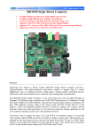
TI-DM3730-EM CORE BOARD User Manual 1 Catalogue 1 2 INTRODUCTIO N .........................................................................................................................................4 1.1 PRO DUC T OVERVIEW ...........................................................................................................................4 1.2 AC RONYMS .............................................................................................................................................4 1.3 TI-DM3730-EM CORE BOARD BLOC K DIAGRAM ...............................................................6 EL ECTRICAL SP ECIFICATIO N ...........................................................................................................6 2.1 HARDWARE .............................................................................................................................................6 2.2 OPERATING CONDITIO NS .....................................................................................................................7 2.3 MEC HANIC AL DATA ...............................................................................................................................8 2.4 PROC ESSOR.............................................................................................................................................8 2.4.1 OMAP35x Processor........................................................................................................................8 2.4.2 OMAP35x Processor Block Diagram...........................................................................................9 2.5 CLOC KS ................................................................................................................................................ 10 2.6 MEMORY .............................................................................................................................................. 11 2.6.1 Mobile DDR and NA ND .............................................................................................................. 11 2.6.2 External Memory........................................................................................................................... 12 2.7 AUDIO CO DEC ..................................................................................................................................... 12 2.8 DIS PLAY INTER FAC E .......................................................................................................................... 12 2.9 S ERIAL IN TER FAC ES........................................................................................................................... 12 2.9.1 UART1 ............................................................................................................................................. 13 2.9.2 UART2 ............................................................................................................................................. 13 2.9.3 UART3 ............................................................................................................................................. 13 2.9.4 MsSPI ............................................................................................................................................... 14 2.9.5 I2C .................................................................................................................................................... 14 Reserved I2C Addresses................................................................................................................ 14 2.9.6 3 2.10 USB IN TERFAC E ................................................................................................................................. 14 2.11 GP IO ..................................................................................................................................................... 15 2.12 EXPANS IO N/FEATURE OP TIO NS....................................................................................................... 15 SYSTEM INTEGRATIO N ...................................................................................................................... 16 3.1 CO NFIGURATION................................................................................................................................. 16 3.2 R ES ET.................................................................................................................................................... 16 3.2.1 Master Reset (SYS_nRESPWRON) ——Reset I nput ........................................................ 16 3.2.2 TI-DM3730-EM CORE BOARD Reset (SYS_nRESWARM )——Reset output ...............17 3.3 IN TERRUPTS ..........................................................................................................................................17 3.4 JTAG D EBUGGER INTER FAC E .......................................................................................................17 3.5 POW ER MANAGEMEN T ......................................................................................................................17 3.5.1 System Power Supplies ................................................................................................................. 18 3.5.2 System Power Manag ement......................................................................................................... 18 2 3.5.3 Microcontroller .............................................................................................................................. 19 3.6 BOO T MO DES .......................................................................................................................................20 3.7 ES D CO NS IDERATIO NS.......................................................................................................................20 4 MEMO RY & I/O MAPP ING .................................................................................................................. 21 5 CO NNECTOR DESCRIP TION AND FUNCTION ......................................................................... 22 5.1 CO NNEC TO R DESC RIPTIO NS ............................................................................................................ 22 5.2 PIN DES C RIPTIO NS & FUNC TIO NS .................................................................................................. 23 3 1 Introduction 1.1 Product Overview The SOM35x module based on TI’s OMAP35x processor family is a compact, product-ready hardw are and softw are solution that fast forw ards embedded designs. The SOM35x provides high-performance and low -pow er w ithin tight space constraints for applications. SOM35x support Linux-2.6.31、WinCE6.0、Andro id and other embedded operat ing system. SOM35x provides a mass of softw are resources such as DVSDK, OpenG L ES2.0, OGRE and etc. The SOM35x is an off-the-shelf solution that reduces development risks associated w ith the complex design and manufacturing details of the OMAP3 processor, that Speed Time-to-Market. The compact SOM35x is an ideal off-the-shelf solution for applications that include medical devices, barcode readers, mobile Internet devices, Image Capture Machine, GPS and 3D Game machine. The SOM35x allow s for pow erful versatility, compact designs, and long-life products. Picture 1.1 TI-DM3730-EM CORE BOARD 1.2 Acronyms AD C Analog to Dig ital Converter BSP Board Support Package BT B Board-to-board DDR Double Data Rate (RAM) DMA Direct Memory Access 4 ESD Electrostatic Discharge FIFO First In First Out GPIO General Purpose Input Output GPMC General Purpose Memory Controller GPO General Purpose Output IC Integrated Circuit I/O Input/Output IRQ Interrupt Request LCD Liquid Crystal D isplay LDO Low Dropout (Regulator) McBSP Multi-channel Buffered Serial port PCB Printed Circuit Board PCMCI A Personal Computer Memory Card International Association (PC Cards) PHY Physical Layer PLL Phase lock loop PWM Pulse Width Modulation RTC Real Time Clock SDIO Secure Digital Input Output SDRAM Synchronous Dynamic Random Access Memory SOM System on Module SSP Synchronous Serial Port SPI Standard Programming Interface STN Super-Tw isted Nematic(LCD) TFT Thin Film Transistor(LCD) TI Texas Instruments TSC Touch Screen Controller TTL Transistor-Transistor Logic UART Universal Asynchronous Receive Transmit 5 1.3 TI-DM3730-EM CORE BOARD Block diagram Picture 1.2 TI-DM3730-EM CORE BOARD Block diagram 2 Electrical Specification 2.1 Hardware Processor RAM Flash LED SOM interface Interface ARM Cortex-A8 Core up to 720MHz NEON ™ SIMD Co-processor TI OMAP3530 430MHz TMS320C64x+ DSP POWERVR SG™ 2D/3D graphic Accelerat ion 128MByte/256MByte/512MByt e DDR 256MByte/512MByte/1G Byte Nand Flash 1x Pow er LED 2x Programmable LED 4x 0.5mm 60Pin B2 B interface 1x OMAP3 GPMC 总线(full signal output) resource 6 1x OMAP3 DSS bus(full signal output) 1x AV/S- Video output 1x Camera bus(full signal output) 2x SPI bus(1 route multip lex w ith 1 route HSUS B) 3x 4 cable UART(RX、TX、CTS、RTS) 2x MCBSP bus(1 route multip lex w ith 2 route UART) 2x MMC bus(full signal output) 1x HS US B OTG 2x HS US B ULPI bus(full signal output) 2x I2C bus 1x OneWire bus 1x TI standard JTAG 1x stereo headphone output(Dual Channel) 1x Mono Channel microphone input 1x Mono Channel Aud io output 6x extra GPIO(Pow er Management IC derivation, include 2 route PWM) 2x ADC input 5x boot selection signal 5x Pow er management signa( l 2 route system Reset;1 route rouse;2 route external pow er control) 6x6 matrix scanning keyboard 2.2 Operating conditions Condition Minimum Normal Maximum Pow er supply 3.3V 80mA(*1) 3.3V 200mA(*2) 3.3V 500mA(*3) Pow er Consumption 264mW(*1) 660mW(*2) 1650mW(*3) Temperature(Commercial) Temperature(Industrial) 0°C -40°C / / 70°C 80°C 7 *1、Pow er Consumption Condition:SOM53x w ork in a low pow er consumption state and cut dow n all external pow er supply. *2:Pow er Consumption Condit ion:SO M53x w ork in high speed and all the external pow er supply netw ork normally (supply current is the half of the maximum value) *3:Pow er Consumption Condition:SO M53x w ork in maximum speed and the external pow er supply in maximum current speed. 2.3 Mechanical data Primary Purpose OMA P35XSystem on Mo dule PCB size 1.37 x 2.51 inch(34.8 x 63.75mm) Set hole 3 picture2.1 TI-DM3730-EM CORE BOARD PCB size diagram 2.4 Processor 2.4.1 OMAP35x Processor The TI-DM3730-EM CORE BOARD uses TI’s high-performance OMAP35x Applications Processor. This device features the Superscalar ARM® Cortex ™-A8 RISC core and provides many integrated on-chip peripherals, including : 8 Superscalar ARM ® Cortex™- A8 RISC core Vectored floating point un it 16 Kbytes instruction L1 cache 16 Kbytes data L1 cache 64 Kbyte RAM 32Kbyte RO M Integrated LCD Controller 3 UART I2S codec interface One high-speed US B 2.0 On-the-Go(OTG) interface and one high-speed USB 2.0 host interface Many general purpose I/O GPIO signals Programmable timers Real time clock(RTC) Low pow er modes See TI’s OMAP35x TRM and Data Sheet for additional information; the documents are availab le from TI’s w ebsite. 2.4.2 OMAP35x Processor Block Diagram 9 Figure 2.1:OMAP35x Processor Block Diagram NOTE: The block diagram pictured above comes from TI’s OMAP3530/25 App lications Processor Data Sheet. 2.5 Clocks The OMAP35x requires an oscillator and crystal to enable proper internal t iming. A 26.000 MHz oscillator is used to generate many of the processor ’s internal clocks via a series of Phase Lock Loops (PLLs) and signal d iv iders. To generate the core CPU clock, the 26.000 MHz signal is run through a Digital PLL controlled by the PRCM registers. Divisors are used to divide dow n the internal bus frequency to set the LCD, memory controller, camera interface, etc. The second required crystal runs at 32.768 kHz and is connected directly to the TPS65950. The 32.768 kHz clock is used for PMIC and CPU start up and as a reference clock for the Real 10 Time Clock (RTC) Module. The CPU’s microcontroller core clock speed is initialized by softw are on the Torpedo SOM. The DDR SDRAM bus speed is set at 166 MHz in Log icLoader. Other clock speeds, such as core speed and specific serial baud rates, can be supported and modified in softw are for specific user applications. The TI-DM3730-EM CORE BOARD provides an external bus clock, uP_BUS_CLK. This clock is driven by the GPMC_CLK pin. OMA P35x Micro controller TI-DM3730-EM CORE BOARD Net Name Signal Name CORE N/A Default Software Value in X-Loader Up to 600 MHz SDRC_CLK N/A 166 MHz GPMC_CLK uP_BUS_CLK Not configured IMPORTANT NOTE: P lease see TI’s OMAP35x TRM for additional information about processor clocking. 2.6 Memory 2.6.1 Mobile DDR and NAND The OMAP35x uses a 32-bit memory bus to interface to mobile DDR SDRAM and a 16-bit memory bus to interface to NAND. At the time of publication, it can be ordered in three density options: 128 MB Mob ile DDR and 128 MB N AND 256MB Mob ile DDR and 256 MB N AND 512MB Mob ile DDR and 512 MB N AND In TI-DM3730-EM CORE BOARD , the default memory configuration is designated as 256MB Mob ile DDR and 256MB NAND. 11 2.6.2 External Memory It is possible to expand the system’s non-volatile storage capability by adding external flash ICs, SD memory, Compact Flash, or NAND flash. 2.7 Audio Codec The OMAP35x processor has multiple Mu lt i-channel Buffered Serial Port (McBSP) interfaces that support PCM and I2S formats. Both PCM and I2S serial paths drive the built -in TPS65950 audio codec. From the TPS65950, the outputs are CODEC_O UT L and CODEC_ O UTR; these signals are availab le from the expansion connectors. The codec in the TPS65950 performs up to full-duplex codec functions and supports variable sample rates from 8–96k samples per second. 2.8 Display Interface The OMAP35x has a bu ilt-in LCD controller supporting STN, color STN, and TFT panels at a resolution of up to XGA 1024 x 768 x 24-bit color. See TI’s OMAP35x TRM for further information on the integrated LCD controller. The signals from the OMAP35x LCD controller are organized by bit and color and can be interfaced through the expansion connec tors. PardazeshSabz provide 4.3-inch (resolution is 480x272) and 7-inch (resolution is 800x480) TFT touch screen panel. IMPORTANT NOTE: Using the internal graphics controller w ill affect processor performance. Selecting display resolutions and color bits per pixel w ill vary processor busload. 2.9 Serial Interfaces The TI-DM3730-EM CORE BOARD comes w ith the follow ing serial channels : 12 UART1, UART2, UART3, three SPI ports, tw o MCBSP, and tw o I2C ports. If additional serial channels are required, please contact PardazeshSabz. Please see TI-DM3730-EM User Manual for further information regarding serial communications. 2.9.1 UART1 UART1 has been configured as the main SOM35x serial port based on the processor. It is an asynchronous 16C750-compatible UART. This UART provides a high-speed serial interface that uses 64 byte First In / First Out (FIFO) and is capable of sending and receiving serial data simultaneous ly. The signals from the Torpedo SOM are 1.8V Transistor -Transistor Logic (TTL) level signals, not RS232 level signals. The end-product design must provide an external RS232 transceiver for RS232 applications. When choosing an RS232 transceiver, the designer should keep in mind cost, availab ility, ESD protection, and data rates. The UARTA baud rate is set to a default 115.2 Kb its/sec, though it supports most common serial baud rates. 2.9.2 UART2 Serial Port UART3 is an asynchronous 16C750-compatible UART. This UART is a high-speed serial interface that uses FIFO and is capable of sending and receiving serial data simultaneous ly. The signals from the Torpedo SOM are 1.8V TTL level sign als, not RS232 level sign als. The UART2 baud rate can also be set to most common serial baud rates. 2.9.3 UART3 Serial port UART3 is an asynchronous 16C750-compatible UART. This UART is a high-speed serial interface that uses FIFO and is capable of sending and receiving serial data simultaneous ly. The signals from the TI-DM3730-EM CORE BOARD are 1.8V TTL level signals, not RS232 level signals . The UARTC baud rate can also be set to most common serial baud rates. 13 2.9.4 MsSPI The Torpedo SOM provides three external SPI ports w ith multip le chip selects. Addit ional SPI ports are availab le through different resistor populations. Please see Table 5.1 for more information. 2.9.5 I2C The TI-DM3730-EM CORE BOARD supports tw o dedicated external I2C ports. The cloc k and data signals for the I2C2 port have 4.7K ohm pull-up resistors; the clock and data signals for the I2C3 port have 470 ohm pull-up resistors. Please see TI’s OMAP35x TRM for further information. 2.9.6 Reserved I2C Addresses The OMAP35x Torpedo SOM contains a product ID chip that connects to the I2C bus. PardazeshSabz softw are uses this product ID chip to determine hardw are version information. As a result, the 7-bit I2C addresses listed below are used by the product ID chip and must be avoided in custom designs: 101 1000 101 1001 101 1010 101 1011 101 1100 101 1101 2.10 USB Interface The TI-DM3730-EM CORE BOARD supports one USB 2.0 OTG port, w hich can function as a host or device/client. The port can operate at up to 480 Mbit/sec. For more information on using the OTG 14 interfaces, please see TI’s OMAP35x TRM. IMPORTANT NOTE: In order to correctly implement US B on the SOM3530 -B2, additional impedance matching circuitry may be required on the USB2_D+ and US B2_D- signals before they can be used. US B 2.0 requirements specify the signals must be routed as differential pairs w ith 90 ohm differential impedance. Refer to the USB 2.0 Specification for detailed information. 2.11 GPIO PardazsehSabz design ed the TI-DM3730-EM CORE BOARD to be flexib le and provide mult ip le options for analog and dig ital GPIO. There are numerous digital GPIO pins on the Torpedo SOM that interface to the OMAP35x processor and TPS65930 PMIC; see Section 5 ―Pin Descriptions & Functions‖ for more information. If certain peripherals are not desired, such as the LCD controller, chip selects, IRQs, or UARTs, then more GPIO pins become availab le. 2.12 Expansion/ Feature Options The TI-DM3730-EM CORE BOARD w as designed for expansion and a variable feature set, providing all the necessary control signals and bus signals to expand the user ’s design. It is possible for a user to expand the TI-DM3730-EM CORE BOARD ’s functionality even further by adding host bus or ISA bus devices. Some features that are implemented on the OMAP35x, but are not discussed herein, include: RTC, pulse w idth modulation (PWM), Secure Digital, MMC cards, SDIO cards, graphics accelerator, DSP codecs, Image Processing Unit, 1w ire interface, and the debug module. 15 3 System Integration 3.1 Configuration OMAP35x TI-DM3730-EM CORE BOARD w as designed to meet multip le app licat ions for users w ith specific design and budget requirements. As a result,this TI-DM3730-EM CORE BOARD supports a variety of embedded operating systems and hardw are configurations. Please contact PardazeshSabz Sales for additional hardw are configurations to meet your application needs. 3.2 Reset TI-DM3730-EM CORE BOARD SYS_nRESPWRON ) and a has a reset reset input ( output (SYS_nRES WARM).External dev ices can drive MSTR_nRST low to assert reset to the product.TI-DM3730-EM CORE BOARD uses SYS_nRES WARM to ind icate to other devices that the Torpedo SOM is in reset. 3.2.1 Master Reset(SYS_nRES PWRON)——Reset Input TheMSTR_nRST triggers a pow er-on-reset event to the OMAP35x processor and resets the entire CP U. IMPORTANT NOTE: MSTR_nRST does not reset the TPS65930; the TPS65930 is only reset by removing pow er from the SOM. IMPORTANT NOTE: Any custom reset circuit design should guard the assertion of the reset lines during a low pow er state so as to prevent pow er-up in a low or bad pow er condition. Low Pulse on SYS_nRESPWRO N Signal: A low pulse on the MSTR_nRST signal, asserted by an external source(for example, the reset button on the custom design application),w ill bring SYS_nRESPWRON low until the assertion source is de-asserted. There is no delay beyond the de-assertion of the external 16 SYS_nRESPWRON signal source,so the custom design must ensure that the assertion time is sufficient for all relat ed. 3.2.2 TI-DM3730-EM CORE BOARD Reset(SYS_nRES WARM )——Reset output All hardw are peripherals should connect their hardw are-reset pin to the SYS_nRESWARM signal on the expansion connec tor. Internally, all Torpedo SOM peripheral hardw are reset pins areconnected to the SYS_nRESWARM net. 3.3 Interrupts The OMAP35x incorporates the ARM Cortex- A8 interrupt controller w hich provides many intersystem. Most external GPIO signals can also be configured as interrupt inputs by configuring their pin control registers. PardazeshSabz BSP’s setup and process all onboard systern and external TI-DM3730-EM CORE BOARD interrupt sources. Refer to TI’s OMAP35x TRM for further information on using interrupts. 3.4 JTAG Debugger Interface The JTAG connection on the OMAP35x allow s recovery of corrupted flash memory, real-tim e app licat ion debug, and DSP developm ent. There are several third-party JTAG debuggers availab le for TI microcontrollers. The follow ing signals make up the JTAG interf ace to the OMAP35x processor: TDI, TMS, TCK, TDO, nTRST, RTCK, EMU0, and EMU1. When lay ing out the 20-pin connector, realize that it may not be numbered as a standard 20-pin 0.1‖ insulation disp lacement connector (IDC) through-hole connector. Each JTAG tool vendor may define the 20-pin IDC connector pin-out differently. 3.5 Power Manage ment 17 3.5.1 System Power S upplies In order to ensure a flexib le design, the Torpedo SOM has the follow ing pow er areas: VDD_SOM and VDD_ RTC。All pow er areas are inputs to the TI-DM3730-EM CORE BOARD 。The module also provides VIO_1V8 as a reference voltage. It may be used to supply up to 200 mA of pow er, but it is recommended to use an external supply. 1) VDD_SOM The VDD_SOM input is the main source of pow er for the TI-DM3730-EM CORE BOARD . This input expects a voltage w ithin typ ical sing le lith ium- ion battery lim its w hich generally operate from 2.7V to 4.2V. If a lithium- ion battery is not used as the main pow er source, it is recommended to supply a fixed 3.3 V supply. The TPS65930 pow er management controller takes the VDD_SOM rail input and creates all onboard voltages. If the design is required to maintain RAM contents in a critical pow er situation (e.g., low battery, loss of pow er), the VDD_SOM supply should be maintained above the min imum level at a ll costs. w e suggest using the Standby mode to prepare the system for a critical pow er condition. In this w ay, the DDR SDRAM is placed into self-refresh and the processor is placed into the Standby state. 2) VDD_RTC The VDD_RTC pow er rail for pow er supply board TPS65930。Pow er management state machine, and RTC circuit w hen VDD_SOM is not present. A lithium- ion coin cell typ ically supplies pow er to this rail. The TPS65930 overrides this input w hen VDD_SOM is app lied. 3.5.2 System Power Manage ment Good pow er management design is important in any system development and embedded system design is no exception. In embedded system design, pow er management is typically one of the most complicated areas due to the dramatic effect it has on product cost, performance, usability, and overall customer satisfaction. Many factors affect a pow er-efficient hardw are design: pow er 18 supply selection (efficiency), clocking design, IC and component selection, etc. On the OMAP35x there are many different softw are configurations that drastically af fect pow er consumption: m icrocontroller core clock frequency, bus clock frequency, peripheral clocks, bus modes, pow er management states; peripheral pow er states and modes; product user scenarios; interrupt handling; and d isp lay settings (resolution, backlight, refresh, bits per pixel, etc). These settings are typically init ialized in the startup softw are routines and may be modified later in the operating system and application softw are. T2_REGEN is an open drain output from the TPS65930. It can be used to control pow er for external pow er ICs or LDOs. Please see the TPS65930 TRM for more information. 3.5.3 Microcontroller The OMAP35x processor ’s pow er management scheme w as designed for the cellu lar handset market, w hich means the static and dynamic pow er consumption has very flexib le controls allow ing designers to tw eak the processor to minim ize end-product pow er consumption. 1) Run State The OMAP35x can enter Run mode from any state. A Standby-to-Run transition occurs on any valid w akeup event, such as the assertion or any enabled interrupt signal. All required pow er supplies are active in this state. 2) Suspend State Suspend is the hardw are pow er-dow n state for the SOM.,allow ing for low er pow er consumption. The Suspend state is designed to reduce pow er consumption w hile the OMAP35x is w aiting for an event, such as a keyboard input. In BSPs,All pow er supplies remain active and system context is retained. An internal or external w akeup event can cause the processor to transition back to Run mode. 3) Standby State Standby is the low est pow er state for the SOM. This state is entered in ParcazeshSabz BSPs through softw are commands. The OMAP35x processor is put into the low est pow er state and all clocks are 19 stopped. The VDD_SOM pow er rail should be maintained if the low-pow er DDR SDRAM contents w ish to be retained. Internal or external w akeup events can cause a return to the Run state. 3.6 Boot Modes The OMAP35x provides the option of booting from multiple sources. The boot mode is controlled by the SYS_ BOOT pins of the processor. SYS_BOOT0 and SYS_ BO OT5 are availab le off-board through the expansion connectors. OMA P35x Processor Pins Boot Method Default SYS_ BOOT[6:0]=1101111 Alternate S YS_ BOOT[6:0]=1001111 US B, UART3,MMC1,N AND NAND, US B, UART3,MMC1 Alternate S YS_ BOOT[6:0]=1001110 Alternate S YS_ BOOT[6:0]=1000110 XIPw ait, DOC,USB, UART3,MMC1 MMC1 US B 3.7 ESD Cons iderations The TI-DM3730-EM CORE BOARD w as designed to interface to a customer ’s peoard, w hile remain ing low cost and adaptable to many different applications. The TI-DM3730EM CORE BOARD does not provide any onboard ESD protection circuitry—this must be provided by the product it is used in. 20 4 Memory & I/O Mapping On the OMAP35x microcontroller, all address mapping for the GPMC chip select signals is listed below. Mapped ―Chip Select‖ signals for the OMAP are availab le as outputs from the microcontroller and are assigned as follow s: Chip select Device/Feature Notes nCS0 nCS1 uP_nCS0 uP_nCS1 For NandFlash Non Availab le nCS2 nCS3 uP_nCS2 uP_nCS3 Non Availab le Availab le for use by an nCS4 uP_nCS4 off-board external Availab le for use off-board external by an nCS5 uP_nCS5 Availab le for use off-board external by an nCS6 uP_nCS6 by an nCS7 uP_nCS7 Availab le for use off-board external Availab le for use off-board external by an NOTE:Me mory addres s es for chip s elects on the OMAP35x a re configurable by s oftware; Therefore , precis e addres s locations cannot be provided. 21 5 Connector description and function IMPORTANT NOTE:The follow ing pin descriptions and states are provided by the default pin usage. the signal of defined in the connection table ,lots of that can be configured as input or output—---- Most of the OMAP35x processors can be configured as GPIO input or output of other ------- and have different functions。It is essential to review the final design (includ ing electrical and softw are) all the signals, to verify the necessary configuration(external pu ll-ups/pull-dow ns). IMPORTANT NOTE:Please pay special attention to the reference voltage of the OMAP35x used to pow er each signal in the tab le below, especially w hen used as a GPIO. Not all pow er rails coming out of the TPS65930 are on by default and may need to be enabled through softw are. 5.1 Connector Descriptions Connector list Connector Connector description No. Remark J1 J2 SOM connector SOM connector 0.5mm 60Pin B2 B Male 0.5mm 60Pin B2 B Female J3 J4 SOM connector SOM connector 0.5mm 60Pin B2 B Male 0.5mm 60Pin B2 B Female LED list LED No. D1 LED description Programmable LED Remark T2.LED B D2 D3 Programmable LED Pow er LED T2.LEDA Power List Po wer network Voltage Max Direction Remark VDD_SO M VDD_IO 3.3V 1.8V 1A 500mA Input Output Pow er Input of SOM35x I/O reference voltage output VDD_ MMC1 VBUS_ HS US B0 VDD_ RTC 1.8V/3 V 5V 3V 220mA 100mA Output Output Input MMC1 pow er output US B OTG pow er output RTC battery input VDD_ AUX2 1.8V 100mA Output Controllab le 1.8V pow er output 22 Test Point list Label circuit Key TP1 TP2 T2.HFCLKO UT VDD_ MP U 1.8V 26MHz 1.2V TP3 TP4 VDD_P LL VDD_D AC 1.8V 1.8V TP5 TP6 TP7 VDD_ MMC1 VDD_ AUX2 VDD_ CORE 3V 1.8V 1.2V TP8 VDD_IO 1.8V 5.2 Pin Descript ions & Functions J1 Connector Pin Descriptions GPIO Pin Signal Name 1 GND No. / I/O Voltage Remark / Ground 3 5 GPMC_ A 10 GPMC_ A9 43 42 1.8V 1.8V 7 9 11 GPMC_ A8 GPMC_ A7 GPMC_ A6 41 40 39 1.8V 1.8V 1.8V 13 15 GPMC_ A5 GPMC_ A4 38 37 1.8V 1.8V 17 19 GPMC_ A3 GPMC_ A2 36 35 1.8V 1.8V 21 23 GPMC_ A1 GND 34 / 1.8V / 25 GPMC_D0 / 1.8V 27 GPMC_D1 / 1.8V 29 31 GPMC_D2 GPMC_D3 / / 1.8V 1.8V 33 35 GPMC_D4 GPMC_D5 / / 1.8V 1.8V 37 39 41 GPMC_D6 GPMC_D7 GPMC_D8 / / 44 1.8V 1.8V 1.8V 43 45 GPMC_D9 GPMC_D10 45 46 1.8V 1.8V 47 49 GPMC_D11 GPMC_D12 47 48 1.8V 1.8V Ground 23 51 GPMC_D13 49 1.8V 53 55 GPMC_D14 GPMC_D15 50 51 1.8V 1.8V 57 59 GND GND / / / / Ground Ground Pin Signal Name I/O Voltage Remark 2 4 GND GPMC_nWE GPIO No. / / / 1.8V Ground 6 GPMC_nOE / 1.8V 8 GPMC_nCS3 54 1.8V 10 GPMC_nCS4 55 1.8V 12 GPMC_nCS5 56 1.8V 14 16 GPMC_nCS6 GPMC_nCS7 57 58 1.8V 1.8V 18 20 GPMC_n BE0_CLE GPMC_n BE1 60 61 1.8V 1.8V 22 24 GPMC_n AD V_ ALE GPMC_nWP / 62 1.8V 1.8V 26 GPMC_WAIT3 65 1.8V 28 GPMC_CLK 59 1.8V 30 32 34 GND MCSPI1_CLK MCSPI1_SIMO / 171 172 / 1.8V 1.8V 36 38 MCSPI1_SOMI MCSPI1_CS0 173 174 1.8V 1.8V 143 1.8V 140 1.8V 141 1.8V 40 42 44 MCBSP3_FSX/UART2_R X MS BSP3_DX/UART2_CT S MCBSP3_DR/ UART2_RT S 46 MCBSP3_CLKX/ UART2_ TX 142 1.8V 48 50 UART1_TX UART1_RTS 148 149 1.8V 1.8V 52 54 UART1_CTS UART1_EX 150 151 1.8V 1.8V 56 58 GND SYS_CLKO UT1/GPIO10 / 10 / 1.8V 60 SYS_CLKO UT2/GPIO186 186 1.8V Ground Ground 24 J2 Connector Pin Description GPIO Pin Signal Name 1 GND No. / I/O Voltage Remark / Ground 3 DSS_VS YNC 68 1.8V 5 DSS_HS YNC 67 1.8V 7 9 DSS_ACBI AS DSS_PCLK 69 66 1.8V 1.8V 11 13 GND DSS_D23 / 93 / 1.8V 15 17 DSS_D22 DSS_D21 92 91 1.8V 1.8V 19 21 DSS_D20 DSS_D19 90 89 1.8V 1.8V 23 25 DSS_D18 DSS_D17 88 87 1.8V 1.8V 27 29 31 DSS_D16 DSS_D15 DSS_D14 86 85 84 1.8V 1.8V 1.8V 33 DSS_D13 83 1.8V 35 DSS_D12 82 1.8V 37 39 DSS_D11 DSS_D10 81 80 1.8V 1.8V 41 43 DSS_D9 DSS_D8 79 78 1.8V 1.8V 45 DSS_D7 77 1.8V 47 DSS_D6 76 1.8V 49 51 DSS_D5 DSS_D4 75 74 1.8V 1.8V 53 55 DSS_D3 DSS_D2 73 72 1.8V 1.8V 57 59 DSS_D1 DSS_D0 71 70 1.8V 1.8V Pin Signal Name GPIO No. I/O Voltage Remark 2 4 GND HDQ_SIO/GPIO170 / 170 / 1.8V Ground 6 8 UART3_CTS_RCTX UART3_RTS_SD 163 164 1.8V 1.8V 10 12 UART3_RX_IRRX UART3_TX_IRTX 165 166 1.8V 1.8V 14 GND / / Ground Ground 25 16 CAM_PCLK 97 1.8V 18 20 CAM_ HS CAM_ VS 94 95 1.8V 1.8V 22 24 CAM_XCLKA CAM_XCLKB 96 111 1.8V 1.8V 26 28 CAM_FLD CAM_WEN 98 167 1.8V 1.8V 30 32 CAM_STRO BE CAM_D0 126 99 1.8V 1.8V 34 36 CAM_D1 CAM_D2 100 101 1.8V 1.8V 38 CAM_D3 102 1.8V 40 42 CAM_D4 CAM_D5 103 104 1.8V 1.8V 44 46 CAM_D6 CAM_D7 105 106 1.8V 1.8V 48 CAM_D8 107 1.8V 50 CAM_D9 108 1.8V 52 54 CAM_D10 CAM_D 11 109 110 1.8V 1.8V 56 GND / / 58 AV/S VID EO_ Y / / 60 SVIDEO_ C / / output Y channel S-Video output C channel I/O Voltage Remark Ground CVBS output/S-Vid eo J3 Connector Pin Descriptions MMC2_D AT7 GPIO No. 139 1.8V 3 5 MMC2_D AT6 MMC2_D AT5 138 137 1.8V 1.8V 7 9 MMC2_D AT4 MMC2_D AT3 136 135 1.8V 1.8V 11 13 MMC2_D AT2 MMC2_D AT1 134 133 1.8V 1.8V 15 17 MMC2_D AT0 MMC2_ CLK 132 130 1.8V 1.8V 19 21 MMC2_ CMD GND 131 / 1.8V / 23 25 HS US B2_D7 HS US B2_D6 178 181 1.8V 1.8V 27 HS US B2_D5 180 1.8V Pin Signal Name 1 Ground 26 29 HS US B2_D4 179 1.8V 31 HS US B2_D3 182 1.8V 33 HS US B2_D2 177 1.8V 35 37 HS US B2_D1 HS US B2_D0 29 28 1.8V 1.8V 39 HS US B2_NXT 27 1.8V 41 HS US B2_DIR 26 1.8V 43 45 HS US B2_STP HS US B2_ CLK 25 24 1.8V 1.8V 47 49 GND PREDRI V.RIG HT / / / / Ground Right aud io output 51 53 PREDRI V.LEFT GND / / / / Left audio output Ground 55 GND / / Ground 57 59 VDD_IO VDD_IO / / / / 1.8V IO output 1.8V IO output Pin Signal Name GPIO No. 13 I/O Voltage Remark 12 1.8V 22 1.8V 23 1.8V 14 1.8V 15 GPIO15 HS US B2_D2/ MCSPI3_CS0/G 16 PIO16 1.8V 16 18 HS US B2_D3/GPIO21 HS US B2_D4/GPIO18 21 18 1.8V 1.8V 20 22 HS US B2_D5/GPIO19 HS US B2_D6/GPIO20 HS US B2_D7/ MCSPI3_CLK/ GPIO17 19 20 1.8V 1.8V 17 1.8V 26 28 GND SYS_nRESPWRON / / / 1.8V Ground Pow er on signal 30 32 SYS_nRESWARM GND / / 1.8V / Warm reset signal Ground 34 36 T2.LEDSYN C/T2.GPIO.13 T2.PWR_ON / / 1.8V 1.8V POWERON signal 38 40 T2.REGEN T2.SYSEN / / 1.8V 1.8V REG EN signal SYSEN signal 2 4 6 8 10 12 14 24 HS US B2_ CLK/GPIO13 HS US B2_STP/GPIO12 HS US B2_DIR/S YS_DRM_M SECURE/GPIO22 HS US B2_NXT/GPIO23 HS US B2_D0/ MCSPI3_SIMO/ GPIO14 HS US B2_D1/ MCSPI3_SOMI/ 1.8V 1.8V 27 42 MICIN / / Mic input 44 46 MICGND AUX R / / / / Mic GND Aud io Input 48 50 GND T2.KPD_C0 / / / 1.8V Ground Square Scan Key C0 52 54 T2.KPD_C1 T2.KPD_C2 / / 1.8V 1.8V Square Scan Key C 1 Square Scan Key C 2 56 58 T2.KPD_C3 T2.KPD_C4 / / 1.8V 1.8V Square Scan Key C 3 Square Scan Key C 4 60 T2.KPD_C5 / 1.8V Square Scan Key C 5 J4 Connector Pin Descriptions Pin Signal Name GPIO No. I/O Voltage Remark 1 3 VDD_ MMC1 MMC1_ CMD / 121 / VDD_ MMC1 MMC1 Pow er 5 MMC1_ CLK 120 VDD_ MMC1 7 9 MMC1_D AT0 MMC1_D AT1 122 123 VDD_ MMC1 VDD_ MMC1 11 MMC1_D AT2 124 VDD_ MMC1 13 MMC1_D AT3 125 VDD_ MMC1 15 17 MMC1_D AT4 MMC1_D AT5 126 127 VDD_ MMC1 VDD_ MMC1 19 21 MMC1_D AT6 MMC1_D AT7 128 129 VDD_ MMC1 VDD_ MMC1 23 25 T2.MMC1_CD/T2.GPIO0 GND / / 1.8V / MMC1 check Ground 27 HS US B0_ID / 3V US B OTG ID 29 HS US B0_DN / 3V US B OTG DN 31 33 HS US B0_DP VBUS_ HS US B0 / / 3V / US B OTG DP US B OTG Pow er 35 37 39 T2.GPIO1 T2.GPIO2 T2.GPIO6/T2.PWM0 / / / 1.8V 1.8V 1.8V 41 43 T2.GPIO7/T2.PWM1 T2.GPIO15 / / 1.8V 1.8V 45 47 T2.ADCIN0 T2.ADCIN2 / / / / 0V~1.5V 0V~2.5V 49 51 VDD_ AUX2 VDD_ RTC / / / / RTC Pow er Input 53 55 GND GND / / / / Ground Ground 28 57 VDD_SO M / / SOM Pow er Input 59 VDD_SO M / / SOM Pow er Input Pin Signal Name GPIO No. I/O Voltage Remark 2 4 MCBSP1_CLKR/GPIO156 MCBSP1_FSR/GPIO157 156 157 1.8V 1.8V 6 8 10 MCBSP1_DX/GPIO158 MCBSP1_DR/GPIO159 MCBSP1_FSX/GPIO161 158 159 161 1.8V 1.8V 1.8V 12 MCBSP1_CLKX/GPIO162 162 1.8V 14 SYS_ BOOT5 7 1.8V Don’t using as GPIO 16 SYS_ BOOT4 6 1.8V Don’t using as GPIO 18 SYS_ BOOT3 5 1.8V Don’t using as GPIO 20 22 SYS_ BOOT2 SYS_ BOOT1 4 3 1.8V 1.8V Don’t using as GPIO Don’t using as GPIO 24 26 SYS_ BOOT0 I2C3_SCL 2 184 1.8V 1.8V Don’t using as GPIO 28 30 I2C3_SDA I2C2_SCL 185 168 1.8V 1.8V 32 I2C2_SDA 183 1.8V 34 JTAG_TDO / 1.8V 36 38 40 JTAG_nTRST JTAG_TMS JTAG_TDI / / / 1.8V 1.8V 1.8V 42 44 JTAG_TCK JTAG_RTCK / / 1.8V 1.8V 46 48 JTAG_EMU0 JTAG_EMU1 11 31 1.8V 1.8V 50 52 T2.KPD_R0 T2.KPD_R1 / / 1.8V 1.8V Square Scan Key R0 Square Scan Key R1 54 56 T2.KPD_R2 T2.KPD_R3 / / 1.8V 1.8V Square Scan Key R2 Square Scan Key R3 58 60 T2.KPD_R4 T2.KPD_R5 / / 1.8V 1.8V Square Scan Key R4 Square Scan Key R5 29