1
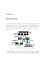
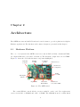
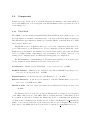
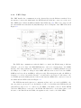
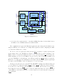
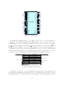
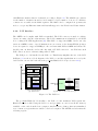
Universitatea ”POLITEHNICA” Bucureşti
Facultatea de Electronică şi Telecomunicaţii
Catedra de Electronică Aplicată şi Ingineria Informaţiei
An FPGA-based Platform for the Performance
Evaluation of Ethernet Networks
Doctorand: ing. Matei Dan CIOBOTARU
Conducător ştiinţific: prof. dr. ing. Vasile BUZULOIU
December 15, 2005
Abstract
Ethernet is the underlying technology for the Trigger and Data Acquisition (TDAQ)
system that will be used in the ATLAS experiment at CERN. The TDAQ will employ a large
high-speed Ethernet network, comprising several hundred nodes. Ethernet switches will handle
all the data transfers, their performance being essential for the success of the experiment. We
designed and implemented a system called the GETB (Gigabit Ethernet Testbed), which can
be used to assess the performance of network devices. This report introduces the architecture
and the implementation of the GETB platform, as well as its applications. The main project,
the GETB Network Tester, will be presented in-depth. The features of the system will be
described and sample results will be presented.
Contents
1 Introduction
1.1
Motivation
3
. . . . . . . . . . . . . . . . . . . . . . . . . . . . . . . . . . . . .
2 Architecture
4
6
2.1
Hardware Platform . . . . . . . . . . . . . . . . . . . . . . . . . . . . . . . . .
6
2.2
Components . . . . . . . . . . . . . . . . . . . . . . . . . . . . . . . . . . . . .
8
2.2.1
The FPGA . . . . . . . . . . . . . . . . . . . . . . . . . . . . . . . . .
8
2.2.2
PHY Chips . . . . . . . . . . . . . . . . . . . . . . . . . . . . . . . . .
9
2.2.3
GPS Card . . . . . . . . . . . . . . . . . . . . . . . . . . . . . . . . . .
10
2.2.4
RJ45 Connectors . . . . . . . . . . . . . . . . . . . . . . . . . . . . . .
11
2.2.5
Ethernet MAC . . . . . . . . . . . . . . . . . . . . . . . . . . . . . . .
11
2.2.6
PCI Interface . . . . . . . . . . . . . . . . . . . . . . . . . . . . . . . .
14
2.2.7
SRAM and SDRAM Memories . . . . . . . . . . . . . . . . . . . . . .
15
2.2.8
Handel-C Application Code . . . . . . . . . . . . . . . . . . . . . . . .
16
Control Software . . . . . . . . . . . . . . . . . . . . . . . . . . . . . . . . . .
17
2.3
3 The Network Tester
3.1
18
Features . . . . . . . . . . . . . . . . . . . . . . . . . . . . . . . . . . . . . . .
18
3.1.1
Transmission – Independent Generators . . . . . . . . . . . . . . . . .
18
3.1.2
Transmission – Client-Server . . . . . . . . . . . . . . . . . . . . . . .
19
1
3.1.3
Receive path . . . . . . . . . . . . . . . . . . . . . . . . . . . . . . . .
20
3.2
Implementation . . . . . . . . . . . . . . . . . . . . . . . . . . . . . . . . . . .
21
3.3
Operation . . . . . . . . . . . . . . . . . . . . . . . . . . . . . . . . . . . . . .
23
4 Sample Results
24
4.1
Fully-Meshed Traffic Performance . . . . . . . . . . . . . . . . . . . . . . . . .
24
4.2
Size of the MAC Address Table . . . . . . . . . . . . . . . . . . . . . . . . . .
26
4.3
Quality of Service (QoS) Tests . . . . . . . . . . . . . . . . . . . . . . . . . .
27
4.4
Buffering capacity and the ATLAS traffic pattern . . . . . . . . . . . . . . . .
28
5 Other Applications
30
5.1
The ATLAS ROB Emulator . . . . . . . . . . . . . . . . . . . . . . . . . . . .
30
5.2
Network Emulator . . . . . . . . . . . . . . . . . . . . . . . . . . . . . . . . .
31
6 Conclusion
32
2
Chapter 1
Introduction
The ATLAS Trigger and Data Acquisition system (TDAQ) is responsible for the real-time
filtering and transfer of the data generated by the ATLAS detector [1]. The input event rate
of 40 MHz produced by the detector is progressively reduced by the TDAQ system down to
200 Hz. The filtering is done using massive computing resources which are interconnected in
a large high speed network. Figure 1.1 shows a schematic diagram of the central part of the
TDAQ network.
Figure 1.1: The ATLAS TDAQ Network – Schematic block diagram.
The TDAQ system is organized in three levels that process detector data. Level 1 (LVL1)
uses dedicated hardware to perform the first selection of events. The interesting data selected
by LVL1 are stored temporarily into Read Out Buffers (ROBs) over 1600 links. Data fragments
3
related to an event are distributed to all the ROBs. The next filtering stage is performed by
algorithms running on the Level 2 computing farm (LVL2). The LVL2 processing units (L2PU)
use the Region of Interest (RoI) information available from LVL1 to collect data from only a
relevant subset of the ROBs and to analyze the event. When the L2PU reaches a decision, it
is announced to the LVL2 supervisor (L2SV). The L2SV forwards the LVL2 decision to the
DataFlow Manager (DFM), which coordinates the assembly process of the validated events.
The DFM assigns a Sub-Farm Interface node (SFI) to gather all the data available for an
event selected by LVL2. The SFI asks the ROBs to deliver all 1600 event fragments. When a
full event is stored in the SFI, the DFM sends a “clear” message to all the ROBs announcing
that they can free their buffers (the DFM also sends “clear” messages for events rejected by
the LVL2). The SFI is the entry point to the third level of filtering, the Event Filter, which
performs more complex physics algorithms on complete events.
The sustained data rates required for the system to operate properly are quite demanding
(see Figure 1.1); for example an SFI receives data from the ROBs at a rate of ≈60MB/s
[2]. The technology chosen for the TDAQ network is Gigabit Ethernet (GE) [3]. The core
network will be Layer 2 only; meaning that all data transfers will be handled by Ethernet
switches (no Layer 3 IP routing). The need for minimal network latency and minimal packet
loss imposes strict performance requirements on the switches. Therefore, each device that will
be used in the network will undergo an evaluation process to make sure that it meets system
requirements. In this report we present the system created for this purpose.
1.1
Motivation
A set of performance metrics and test procedures has been defined in order to check the
compliance of candidate devices for the ATLAS TDAQ network [4]. These procedures try to
characterize the performance aspects that will be relevant for the final ATLAS data-taking
phase. Commercial network testing equipment such as the Ixia Optixia or Spirent Smartbits
is mainly oriented towards protocol compliance and raw performance, lacking the flexibility
needed in defining ATLAS-like traffic patterns.
After researching the market we understood that a programmable platform would better
suit our needs, because in addition to a testing system we also envisioned other networking applications (emulation, monitoring, etc). Our main requirements were top-level performance and full programmability. The necessity of line-speed operation in any circumstances
practically eliminated the possibility of using a general purpose microprocessor. A dedicated
network processor was considered as a potential candidate. Unfortunately these processors
are designed for packet switching applications and are not very well suited for custom traffic
generation.
4
We finally decided that a platform based on an FPGA would be the best choice for the
type of applications we envisioned. Such platforms have been built before. A system similar
to the one described that will be described in the following pages is the GNET-1 [5] that
provides functions for network emulation and traffic generation. Commercial applications
are also available. Celoxica, the company that makes the Handel-C language compiler, has
the RC Series of development platforms, which provide a complete environment that can be
used among other things for networking applications [6]. However, in general, none of these
platforms can be used to build a port density testbed.
Based on our previous experience with hardware-accelerated networking applications (the
FPGA-based FastEthernet Tester and the CPU-based Gigabit Tester [7], [8]) we designed a
new FPGA-based platform called the Gigabit Ethernet Testbed (GETB).
This new platform is fully programmable and delivers Gigabit wire-speed performance; it
also allows us to build a high port density testbed. In the following we describe the architecture
of the GETB platform and we present the projects currently using it. First we describe the
Network Tester, a tool that is being used at present to evaluate network equipment for the
ATLAS TDAQ network. We shall also present sample results obtained using the tester. Two
other projects which are based on the same hardware, will be briefly discussed: the ATLAS
ROB Emulator and the Network Emulator.
5
Chapter 2
Architecture
The GETB uses custom-built PCI cards and control software to provide a platform for Gigabit
Ethernet applications. The hardware and software designs are presented in this chapter.
2.1
Hardware Platform
The core of our system is the GETB card; it is a custom PCI card that contains an FPGA,
two Gigabit Ethernet ports and local memory. The hardware design was done at CERN.
Figure 2.1 shows the card with the main components highlighted.
RJ45 GPS
Connector
Test Header
Card ID
SDRAM
2 x 64Mb
JTAG Connector
Flash memory
(configuration)
SRAM
2 x 512Kb
RJ45 Gigabit
Ethernet
Altera Stratix
EP1S25 FPGA
Gigabit PHYs
PCI Connector
3.3V / 32bit / 33MHz
Figure 2.1: The GETB Card.
The central FPGA controls all the resources available on the card. User applications
can access 128 Mb of SDRAM and 1 Mb of SRAM. The SDRAM is used for tasks which
6
require large amounts of storage space (buffering, traffic description), while the SRAM is
more appropriate for time-critical operations (histograms). Depending on the application,
the two GE ports can be fully independent or data can flow from one port to the other.
The third RJ45 port is used for clock synchronization among multiple cards (via a clock
distribution system); the PCI bus can also be used to synchronize cards in the same chassis.
The main component is the Altera Stratix FPGA, a device containing 25k logic elements.
To simplify the board layout the Ethernet MAC and PCI functionality are embedded in the
FPGA (using IP cores from MoreThanIP and PLDA respectively, [9], [10]). The firmware
contains blocks common to all projects (MAC, PCI, control) plus application dependent
parts (see Section 3.2). Most of the high-level functionality is implemented in the HandelC hardware description language [11]. All projects share a common low-level library that
provides primitives for accessing the memories, routines to simplify the creation of Ethernet
packets and a simplified PCI interface. All of the applications make heavy use of the dual-port
SRAM blocks provided by the Stratix FPGA to implement queues between concurrent and
asynchronous processes.
VHDL glue code is used in the firmware to inter-connect the various blocks (Handel-C
netlist, MAC and PCI cores, SDRAM controllers, etc); for the entire project the size of this
glue code is significant (≈2200 lines). Any design modifications would require manual changes
of the code, an error prone process. To simplify its maintenance we created a tool that takes as
input the names of the blocks and the relationships between them and generates the required
source code (VHDL Gen, [12]); this tool has saved considerable effort.
The compilation of the firmware is done using the Altera Quartus fitter. The Handel-C
compiler creates a netlist that has to be linked against the entities to which it interacts (MAC
and PCI core, SDRAM controllers, etc.). All these connections are created in the top-level
VHDL file created using VHDL Gen. The typical logic resource utilization is about 90% from
which approximatively 50% is the user code. Squeezing the required functionality into the
available resources proved to be a challenge. Multiple clock domains are used – the most
demanding being the Gigabit interface running at 125MHz. The Handel-C user code runs
normally at 41 MHz which is fast enough to keep up with the Gigabit data rates.
The GETB card fits into a standard 3.3V PCI slot. The PCI interface is used to configure
the application firmware, to collect statistics and to perform firmware upgrades. The large
scale testbed is built using many cards mounted in industrial PCs which are interconnected
in a local network. The typical configuration for the large scale GETB testbed is shown in
Figure 2.8 from Section 2.3. Our current setup has 128 GE ports, but there is no technical
limitation on the number of ports in the system.
7
2.2
Components
In this section we describe in more detail the hardware and firmware components which are
used on the GETB card. A block diagram of the FPGA firmware will be presented in Section
3.2 and Figure 3.4.
2.2.1
The FPGA
The GETB board uses an Altera Stratix EP1S25-F780-C7 FPGA. It is a Class 7 device, so it
is not the fastest one available on the market (C5 or C6 devices can run at higher frequencies).
This FPGA has approximatively 25000 logic elements, 2Mbits of internal memory, 6 PLLs
and dedicated DSP blocks.
This FPGA is based on SRAM technology so it loses its configuration when there is no
power. When turned on, the FPGA tries to get its configuration from the Flash chip - if the
Flash was properly written, the firmware is loaded and then started. After this, the FPGA
can be reconfigured using a ByteBlaster cable (a parallel port to JTAG connector) or by
writing a new configuration into the Flash and self-triggering a reconfiguration.
The FPGA firmware contains multiple blocks which run at different clock frequencies (see
below). Details about the firmware are presented in Section 2.2.8.
PCI Interface - Handled by the PLDA PCI core (see Section 2.2.6) – 33 MHz
SDRAM Interface - Handled by two instances of the Altera SDRAM Controller (see Section 2.2.7, about the memories) – 41 MHz
SRAM Interface - Controlled directly by the Handel-C code – 41 MHz
Ethernet Interfaces - Controlled by two instances of the MoreThanIP MAC core (see Section 2.2.5) – 125 MHz and 25 MHz
Handel-C Code - The rest of the logic is inside the two Handel-C blocks (see Section 2.2.8)
– 41 MHz
The FPGA is fed by 2 clocks. On one side the FPGA is fed by a single clock of frequency
of 125 MHz coming from one of the PHYs. This clock signal enters into a PLL (Phase Locked
Loop) which is a special block inside the FPGA that is able to synthesize new frequencies
by division and/or multiplication. In this way the clocks for the Handel-C eth main and the
MAC core are generated (and also for the memories). The second clock signal comes from the
PCI connector (33 MHz) and is used by the PCI core and the pci main Handel-C block.
8
2.2.2
PHY Chips
The PHY handles the communication at the physical layer in the Ethernet standard. It is
the interface between the MAC inside the FPGA and the RJ45 line connectors on the card.
The GETB uses a Marvell 88E1111 Alaska Ultra PHY chip [13]. This device supports all
the current Ethernet standards: 10/100/1000 Gbps. A block diagram of the PHY is shown in
Figure 2.2.
Figure 2.2: Ethernet PHY Block Diagram.
The PHY chip communicates with the MAC core inside the FPGA using 2 different
channels - one is for data - the MII/GMII interface, and one for management - the MDIO
interface. The data path has two distinct modes of operation: for 100Mbps Ethernet it uses
the MII protocol, while for 1Gbps it uses GMII. MII uses 4-bit words clocked at 25MHz.
GMII uses 8-bit words at 125MHz (so 1Gbps in total). The management path, the MDIO, is
designed to be a slow, but reliable, interface – it sends and receives data on only 2 wires – the
clock MDC (from the MAC) and the bidirectional data line MDIO. The connection between
the MAC and the PHY is shown in Figure 2.3.
The PHY has internal registers for configuration (they can be accessed via MDIO) – the
auto-negotiation options can be set, the link speed, and so on. In addition the PHY has special
pins which are supposed to be connected to the LEDS on the RJ45 connector. In the GETB
card these LED pins are connected to the FPGA. The Handel-C code uses these pins to read
the state of the link. From the FPGA, the signals are also routed to the RJ45 LEDs.
9
The Core MII and GMII interface, on the transmit interface are Muxed using the core control
signal eth_mode. The Core pin eth_mode is set to ‘1’ when the Core is programmed (Core
command register ETH_SPEED set to ‘1’ or Core pin eth_mode_set set to ‘1’) to operate in
Gigabit mode and is set to ‘0’ when the Core is programmed to operate in 10/100 mode (Core
command register ETH_SPEED set to ‘0’ and Core pin eth_mode_set set to ‘0’). When
eth_mode is set to ‘1’, the Core GMII interface should be driven to the PHY interface and
when eth_mode is set to ‘0’, the Core MII interface should be driven to the PHY interface.
When configured to operate in 10/100Mbps, the MAC Transmit path should be synchronized
to the 2.5/25MHz from the PHY. When configured to operate in Gigabit mode, the MAC Transmit path should be synchronized with a 125MHz clock derived from the PHY reference clock.
In 10/100 mode, the clock generated by the MAC to the PHY can, for example, be tri-stated.
25MHz
Osc.
25MHz
Reference
Reference
Clock
Clock
x5
2.5 / 25MHz
Clock
Driver
tx_clk
mii_tx_d(3:0)
mii_tx_en
mii_tx_err
gmii_tx_d(7:0)
gmii_tx_en
gmii_tx_err
10/100/1000 PHY
eth_mode
Optional tie to ‘0’ if not used
set_1000
Optional tie to ‘0’ if not used
MAC Core
set_10
Unused
ena_10
rx_clk
mii_rx_d(3:0)
mii_rx_dv
mii_rx_err
125 / 25 / 2.5MHz
gmii_rx_d(7:0)
gmii_rx_dv
gmii_rx_err
FPGA / ASIC
Figure 41: Connection with Standard 10/100/1000 PHY Device
Figure 2.3: MAC to PHY connection.
2.2.3
GPS Card
68
UNH Member
The GETB card was designed to support a global clock synchronization system using a
GPS card. We are using a Meinberg GPS card [14]. The card has a 9pin serial connector
that outputs a 1Hz Pulse per Second (PPS) signal and a 10MHz signal. The 1Hz signal is
synchronized with the GPS satellites – this is the basis of the synchronization system.
The two signals, 1Hz and 10MHz, need to be distributed to all GETB card on the GPS
RJ45 connector. In stand-alone mode this is done using a special serial-to-RJ45 cable. When
multiple cards are used, a GPS fan-out box distributes the signals to all cards. When using
the GPS fan-out box the clocks are sent only to the fan-out box. The 2 GPS signals are in
TTL standard and they need to be converted to LVDS. This is done either using a circuit
embedded in the connector, or in the GPS fan-out box. The FPGA does not accept TTL
inputs (the FPGA I/O pins work at 3.3V, TTL is 5V).
Inside the FPGA there are listeners for the 2 clock signals. There is a PLL that expects
a 10MHz clock as input, a counter that runs with the 10MHz clock, and a Handel-C thread
that listens to the PPS signal.
The GPS fan-out box which is supposed to distribute the GPS signals to all the GETB
cards, hasn’t been built yet. The validation of the GPS system was done in stand-alone mode,
using one GETB card connected directly to the GPS.
10
2.2.4
RJ45 Connectors
There are 3 RJ45 connectors on the board. Two of them are used for the Gigabit ports (the
bigger ones in Figure 2.1) and one for the GPS synchronization. The Ethernet RJ45 data lines
are connected to the PHY chips. The RJ45 LED pins are connected directly to the FPGA
(which routes internally the LED signals from the PHY).
The GPS RJ45 connector is used to receive the clocks from the GPS card (using a handmade cable) or from the GPS fan-out box. There are 4 signals used on this connector:
1Hz PPS (INPUT) - A pulse of duration 0.2seconds that is sent by the GPS card at the
beginning of each second - this signal is synchronized with the UTC time.
10MHz clock (INPUT) - This is coming from an oscillator on the GPS card.
AUX 0 (OUTPUT) - Used for clock synchronization. Connected only to a card which was
assigned the role of ”GETB master”. A pulse is sent by the GETB master card to all
the other cards to trigger various actions.
AUX 1 (INPUT) - Connected to the AUX 0 output from the master card - each GETB card
should receive a copy of the AUX 0 from the master, on the AUX 1 pin.
The 10MHz and 1Hz signal are used in LVDS differential mode. The AUX 1 and AUX 0
cannot be used in differential mode because of the placement of the pins on the FPGA
(they are too close to pins which use single-ended transmission). Because of this, we observed crosstalk between the AUX signals and the GPS clocks (the clocks are corrupted when
something happens on the AUX lines). No solutions have been found to this problem yet.
2.2.5
Ethernet MAC
The MAC is responsible for the creation of Ethernet frames that are sent to the PHY chips.
We are using a ”software” MAC - the Gigabit Ethernet MAC core from MoreThanIP. The
GETB uses 2 instances of the MAC core (one for each Ethernet port). A block diagram of
the MAC core is shown in Figure 2.4. The core works with multiple clocks:
• A 125MHz clock for the data path between the MAC and the PHY (the MII/GMII
interface).
• A client clock for the Handel-C eth main block - currently this is set to 41 MHz.
11
10/100/1000Mbps Ethernet MAC Core
Reference Guide
V3.6 - January 2005
4 MAC Core Block Diagram
Receive Application
Interface
RX Control
CRC Check
Transmit
FIFO
Pause Frame
Terminate
MII / SERDES
Transmit Interface
TX Control
CRC Gen.
GMII / SERDES
Transmit Interface
Transmit Application
Interface
GMII / SERDES
Receive Interface
Receive
FIFO
Loopback
Pause Frame
Generate
PHY Management
Interface
Magic Packet
Detection
Configuration
Statistics
MII / SERDES
Receive Interface
MAC
MDIO
Master
Register Interface
Figure 3: 10/100/1000Mbps Ethernet MAC Core Overview
Figure 2.4: MAC IP Core.
• A clock for the register interface - currently 25MHz. From this clock the MAC derives
the MDC clock for MDIO transactions with the PHY.
The communication between the Handel-C application (the client) and the MAC is done
using two FIFOs (one for TX and one for RX).
Their depth is set when configuring the MAC
10
core and their width is set to 32bits.
UNH Member
In order to send one packet the client sets the ff tx sop signal to 1 (start-of-packet) and
starts writing data to the TX FIFO (see Figure 2.5). Each time we write something to the
FIFO we have to check if the MAC is ready to receive the data using ff tx rdy. Because the
MAC transmits one byte per 125MHz clock cycle and we write 4 bytes per 41MHz clock
cycle, the TX FIFO becomes full quite often. When it is full, the ff tx rdy will be low and the
Handel-C code will pause the transmission and resume when the ready signal is again high
(we wait for the TX FIFO to have enough space to receive new data).
For the receive part we need to check when the RX FIFO contains some valid data that can
be read. This is done using the signals ff rx dsav and ff rx dval. When the data is available,
we are allowed to raise the ff rx rdy and then we can read the data from the port ff rx data.
If the Handel-C client asserts ff rx rdy to 1 then the MAC will change the data at the head
of the FIFO at each client clock cycle - so if the client is not ready, it should de-assert the
ff rx rdy signal.
12
10/100/1000Mbps Ethernet MAC Core
Reference Guide
V3.6 - January 2005
5.2
Core with 32-Bit FIFO Interface
ff_rx_clk
gmii_rx_dv
gmii_rx_d(7:0)
gmii_rx_err
gmii_tx_en
ff_rx_sop
ff_rx_eop
ff_rx_err
gmii_tx_d(7:0)
gmii_tx_err
ff_rx_err_stat(21:0)
ff_rx_ucast
ff_rx_mcast
ff_rx_bcast
ff_rx_vlan
mii_rx_dv
ff_tx_clk
MII Interface
mii_rx_d(3:0)
mii_rx_err
mii_tx_en
mii_tx_d(3:0)
ff_tx_wren
mii_tx_err
ff_tx_data(31:0)10/100/1000Mbps
ff_tx_mod(1:0) Ethernet MAC
ff_tx_sop
ff_tx_eop
ff_tx_rdy
ff_tx_err
ff_tx_crc_fwd
ff_tx_septy
mii_rx_crs
mii_rx_col
Interface
Control
FIFO Transmit
Interface
GMII Interface
FIFO Receive
Interface
tx_clk
ff_rx_mod(1:0)
eth_mode
ena_10
set_10
set_100
xoff_gen
xon_gen
PHY
Management Reset Signals
Pause
Register Interface Command
Clocks
rx_clk
ff_rx_rdy
ff_rx_dsav
ff_rx_dval
ff_rx_data(31:0)
mdc
mdio_in
mdio_out
reg_clk
reg_rden
mdio_oeN
reg_wren
reg_addr(9:2)
reg_din(31:0)
reg_dout(31:0)
reg_busy
reg_sleepN
reg_wakeup
reset_rx_clk
reset_tx_clk
reset_ff_rx_clk
reset_ff_tx_clk
reset_ff_reg_clk
Figure 5: 10/100/1000Mbps Ethernet MAC Core with 32-Bit FIFO Interface Pinout
Figure 2.5: MAC Interface.
12
UNH Member
The MAC has an MDIO interface to the PHY - this is used to control the PHY ( set
configuration, get status information). The MDIO interface works on 2 lines: the bidirectional MDIO line and the clock MDC. The MAC provides 2 separate data lines: mdio in and
mdio out ; plus an output enable signal mdio oeN. These signals are connected in the top-level
VHDL entity of the FPGA to a three-state driver that has one bidirectional output that goes
to the MDIO data pins of the chip. If the PHY MDIO is properly connected to the MAC then
10/100/1000Mbps
Ethernet
MAC the
CoreMAC core detects
the PHY registers are mapped onto special
MAC registers.
Whenever
a read/write to these special mapped registers, it will generate
a MDIO
transaction.
Reference
Guide
V3.6 - January 2005
7 octets
Frame length
PREAMBLE
1 octet
SFD
6 octets
DESTINATION ADDRESS
6 octets
SOURCE ADDRESS
2 octets
VLAN Tag (0x8100)
2 octets
VLAN info
2 octets
0..1500/9000 octets
0..42 octets
4 octets
LENGTH/TYPE
length/type field
Payload length
PAYLOAD DATA
PAD
FRAME CHECK SEQUENCE
EXTENSION (half dup only)
Figure
7: VLAN
Tagged
MAC Frame
Format Overview
Figure
2.6:
Ethernet
Frame
Format.
In certain applications, MAC frames can be tagged with stacked VLANs (Two consecutive
VLAN Tags) with an additional 8-Byte field (Consecutive VLAN Tags and VLAN Info fields)
inserted between the MAC Source Address and the Type/Length Field.
The MAC core expects to receive valid Ethernet frames from the client application. It
7 octets
PREAMBLEon the Ethernet line and also computes
ensures that the minimum inter-frame
gap is respected
1 octet
SFD
the CRC checksum for each6 octets
frame. But is the
responsibility
of the user application to build
DESTINATION
ADDRESS
6 octets
Frame length
SOURCE ADDRESS
2 octets
VLAN Tag (0x8100)
2 octets
13 VLAN info
2 octets
VLAN Tag (0x8100)
2 octets
VLAN info
2 octets
LENGTH/TYPE
0..1500/9000 octets
0..42 octets
4 octets
PAYLOAD DATA
PAD
FRAME CHECK SEQUENCE
EXTENSION (half dup only)
Stacked VLANs
Payload length
valid Ethernet frames, that are formatted according to Figure 2.6. The MAC keeps counters
for the number of frames sent and received, number of bytes, number of errors, etc. All these
counters are accessible in the MAC registers. The MAC can be configured in promiscuous
mode to accept any Ethernet frame and has full support for the FlowControl Pause frames.
PCI Core User's Guide
2.2.6
PCI Interface
1 - PCI Core Basics
The GETB card complies with PCI 2.2 standard. The PCI connector is made for 64bits,
PCI Core User's Guide
but we are using only the 32bit interface. The PCI communication is handled by a PCI IP
This document is the primary reference and technical manual for PLD Applications 32/64-bits PCI
Target and Master/Target core. This technical manual contains a complete2.2.
functional
T ARGETdescription
DATA PATH of
the PCI core and its local interface.
Core coming from PLD Applications [10]. This PCI core supports 66MHz, but we can only
run it at 33MHz because of speed limitations
in our version of the Stratix FPGA (a faster
2.2.1. Data Flow
1.1. G
ENERAL ARCHITECTURE
device
is required
to support 66MHz). So the card runs with PCI at 33MHz and 32bits. We
u Backend logic is responsible for checking s_bar[] during transactions in order to figure out which
spacewith
is targeted3.3V
:
should point out that the card works only
PCI connectors – few PCs have such
u The PCI core provides an integrated solution for interfacing any user application or system to 32-bit
and 64-bit PCI peripheral devices. It is mostly targeted to the add-in card market, including PLD
Applications development/prototyping boards, but can also be used to design other applications. The
core is programmable and customizable : almost all features can be enabled/disabled to suit specific
needs and the core can be adapted to run in any PCI environment. This core is well suited for
programmable logic designs but can also be implemented in ASIC designs.
P C I C o re
PCI connectors, most of them working with 5V PCI.
s _ d a t a _ o u t []
to a l l s p a c e s
0
B A R 0 d a ta
The PCI protocol is handled by the PCI core. This library simplifies the use of the PCI.
P C I B us
s _ d a ta _ in
5
B A R 5 d a ta
In Figure 2.7 we show a block diagram of the PCI core and the signals that are seen by the
u PCI core is built around a central state machine that controls all operations and insure coherency
and synchronization with PCI bus operations. Data transfer is operated by a 32-bit/64-bit bi-directional
registered data path as shown below :
6
E x p . R O M da t a
7
C o n f i g u r a t i on d a ta
back-end. In our case the back-end is the pci main Handel-C block (see Section 2.2.8).
s_ bar[]
Figure 5 - Target data flow
Device
PCI Bus
Backend should typically implement a data multiplexer controlled by s_bar[] in order to select data
source during read transactions. Data inputs selected by this multiplexer must be registered (either
User before or after the multiplexer) and data value is controlled by s_addr[].
Backend
PCI Core
P a ri ty S ig n a ls
PARITY
CO NTROL
- s_data_in[] must be tied to 0’s when a location where no register/memory is implemented is
targeted.
INTERRUPT
SUPPORT
Co n t r ol S i g n a ls
2.2.2. Control Signals
CORE STATE MACHINE
u All target mode transactions are handled with target interface. PCI core provides all necessary
signals to handle and control target-mode data transfers :
TA RGET MODE
CONTROLLER
s_ ad dr
D ata
32/64 B ITS
DATAPATH
s_ read
s_wri te
s_d ata_ out
CONFIGURATION
SPACE
PCI Bus
PCI Core
s_ da ta _in
s _rd busy
s_wrwa it
s _ ab ort
s _d isco
DMA ENG INE
c o n tro l s i g n a ls
Figure 6 - Target interface
Figure 1 - PCI Core Architecture
(a) Architecture
Shaded blocks are implemented in Master/Target core only.
reg isters,
me mory,
pe riph era l s...
(b) Interface to the back-end logic
PCI core provides an address counter, read and write requests signals :
-
s_addr[] is the transaction address counter, automatically incremented at each data transfer
- s_read
is read-request
signal that indicates when backend logic must provide data
Figure 2.7:
The
PCI Core
- s_write is a write-request signals that indicates when backend logic must store data
15
The pci main Handel-C block talks to the PCI core and translates PCI requests into
Handel-C function calls. Using the PCI core and pci main, we can access all the memory
5
available on the card from the host computer. Any PCI device defines, when it is initialized,
a set of memory regions that are visible to the host computer. The GETB card advertises the
following regions:
14
Region 0 (length = 128 bytes) – Special region used to send commands to the card and read
status registers and counters from the Handel-C code.
Regions 1 and 2 (length = 512 Kbytes) – These regions are mapped to the two SRAM
memories available on the GETB card.
Regions 3 and 4 (length = 64 MBytes) – They are mapped to the SDRAM memories on
the card.
The figure below shows how the GETB card is seen by the host computer:
$ /sbin/lspci -v -d 10dc:0313
03:01.0 Ethernet controller: CERN/ECP/EDU: Unknown device 0313
Flags: bus master, slow devsel, latency 64, IRQ 24
Memory at f0300000 (32-bit, non-prefetchable) [size=128]
Memory at f0280000 (32-bit, non-prefetchable) [size=512K]
Memory at f0200000 (32-bit, non-prefetchable) [size=512K]
Memory at f8000000 (32-bit, non-prefetchable) [size=64M]
Memory at f4000000 (32-bit, non-prefetchable) [size=64M]
Capabilities: <available only to root>
#
#
#
#
#
registers
SRAM 0
SRAM 1
SDRAM 0
SDRAM 1
A remark about the PCI initialization: the PCI interface is inside the FPGA and our
FPGA is an SRAM device which does not remember its configuration when powered off.
When the power turns on, the FPGA will try to download its configuration from the Flash
memory chip which is on the card (see Figure 2.1). While this happens, the PCI interface
does not exist. Only after the FPGA is fully configured, it will boot and start running the
firmware (and the PCI core). It is very important that all these steps happen before the host
computer starts to initialize the PCI cards. The GETB card finishes the booting in time, but
for a larger FPGA that needs more time to configure itself, the PCI startup may become an
issue.
2.2.7
SRAM and SDRAM Memories
The GETB card contains two types of memory. The SRAM is a fast memory and is used for
histograms and for other operations which depend on fast access times. The SDRAM is used
to store packet descriptors or to buffer packets – in this case it is more important to have lots
of space and good performance when reading/writing large blocks of data.
For the SRAM we are using two Cypress CY7C1347B chips of 512kbytes of Synchronous
Static RAM. Each memory is organized in 217 locations of 32-bits. The SRAM runs at the
same clock frequency as the Handel-C block and is controlled directly by it.
15
The SDRAM comes as 4 Micron MT48LC16M16A2 chips. These memories have words
of 16-bit and we are using them in pairs such that the FPGA can see 32-bit words. From
the user point of view the memory has 224 (16 million) addresses - but the chip has only 13
address lines. The SDRAM is organized as a matrix, with rows and columns, and the access
is done in two steps: sending first the row address and then the column address. This is why
the SDRAM is not fast for random access. When doing block operations (burst read / write)
the SDRAM needs just to know the address of the beginning of the block so the row / column
access is done only once.
The SDRAM requires a periodic refresh in order to preserve its contents. We are using
the Altera SDRAM Controller for all the SDRAM operations. The controller takes care of
the refresh for the SDRAM and hides the details of row-column addressing.
2.2.8
Handel-C Application Code
Most of the application logic in the GETB FPGA is implemented in Handel-C. There are
two Handel-C clock domains. One handles the PCI interface (pci main) and is common to
all the GETB projects. The other one is called eth main and contains the code that uses the
Ethernet interface.
Pci main is the block that communicates with the PCI core; it runs at 33Mhz. The
pci main block interfaces to the PLDA PCI core and translates the PCI commands (reads and
writes to memory regions) to commands that are sent to the eth main block. The pci main
block does not have direct access to any hardware resource, it is just a layer between the
PCI and the main application code. It sends specific commands to the other block and it
reads back results. The PCI core implements a state machine that is monitored by pci main;
depending on the position in the state diagram, pci main takes appropriate actions using also
the additional data available from the core (addresses and data inputs).
Eth main is where the application-specific code is written – all the other components
in the firmware are common to all the GETB projects. This block runs at 41 MHz in the
GETB Tester and at 50 MHz in the other projects. eth main communicates with pci main
using Handel-C channels and on-chip RAM. The eth main uses the MAC core to generate
and analyze Ethernet packets. This block has access to all the hardware resources on the
card. There are multiple parallel processes which are running inside eth main. There is a
process that handles PCI requests (forwarded from pci main), there are the processes that
handle the transmission and reception of packets (these two are independent), and there are
processes that look after the GPS system. Each of the processes dealing with the Ethernet
ports is instantiated twice (so that each port can run at full speed). See also Section 3.2 and
Figure 3.4.
16
2.3
Control Software
The GETB provides a common control infrastructure for all the derived projects. In order to
drive the system using automated procedures the control system was built using the Python
scripting language [15]. This allows the user to create scripts for running tests in a very simple
and flexible manner. In the following we shall call GETB servers the machines which host
GETB cards (see Figure 2.8). A GETB client is another machine that is used to control the
GETB servers (in Figure 2.8 this is the Control PC). The two types of machines, the GETB
client and server, run (different) Python applications.
GETB Server
GETB Server
Gigabit Ethernet
DUT
Monitoring
GPS Fanout
Control PC
(GETB Client)
DUT (Device Under Test)
Figure 2.8: Typical Testbed Setup (block diagram).
The GETB servers utilize Linux and a Python server application which is responsible
for the configuration, constant monitoring of the cards and the handling of remote client
connections. The communication between the servers and the clients is done using the XMLRPC protocol1 . The GETB client can configure and interrogate a GETB card using XMLRPC requests to the server. We are using a fast implementation of the XML-RPC protocol
which uses only one TCP connection per session2 [16]. For the low-level interaction with the
cards via PCI we use a custom Linux kernel module and its associated library (IO RCC, [17]).
The GETB client application (running on the management workstation or the Control
PC) runs on any machine with a Python interpreter. The client connects using XML-RPC
to all the GETB servers. On the client side each of the two ports of a GETB card is seen
as an individual entity. The physical location of a GETB card (or of a port) is completely
transparent to the user, all ports being seen as independent objects which can be freely
configured. The entire system is controlled from the client PC either using the command line
or by running scripts. A graphical interface is available for displaying the statistics from all
the ports in the system.
1
XML-RPC stands for XML-based Remote Procedure Calls. It allows a remote client to execute functions
on a server and retrieve the results.
2
In the standard XML-RPC implementation, a TCP connection will be created for each RPC request. This
becomes a major bottleneck when there are many requests.
17
Chapter 3
The Network Tester
The main application of the GETB platform is the Network Tester. The aim is to allow us to
evaluate devices (switches) from various manufacturers and to identify those which best suit
the ATLAS TDAQ network needs.
3.1
Features
The Network Tester uses the GETB card to implement a traffic generator and measurement
system. It can send and receive traffic at Gigabit line speed while computing real-time averages for the most important parameters of a flow (packet loss, latency and throughput).
Being an FPGA-based architecture, all processing is done on the hardware without any CPUload on the host system. Two transmission modes are supported: one in which each port is
fully independent of the others (Independent Generators, IG mode) and one in which a port
transmits only when requested by another port (Client Server, CS mode).
3.1.1
Transmission – Independent Generators
In the IG mode each port in the system sends traffic according to a list of packet descriptors loaded into the SDRAM of the card. Each descriptor is used to build one packet. The
firmware uses the fields in each descriptor to build the outgoing packets (Figure 3.1). The
user can configure the Ethernet and IP headers, the inter-packet time (IPG) and packet size
for each descriptor independently, allowing a wide range of traffic patterns to be generated.
For example, a negative-exponential random number generator used for the IPG produces a
Poisson traffic stream. In addition to raw Ethernet and IP packets, special frames like Flow
Control and erroneous frames can be transmitted.
18
Packet
Descriptors
Outgoing
Packets
TX
Figure 3.1: Transmission Modes – Independent Generators (descriptors-based).
As the size of the descriptor list is limited only by memory, by simply cycling through the
list a wide range of traffic patterns can be generated.
3.1.2
Transmission – Client-Server
The second mode of operation – the client-server (CS) or request-reply mode – emulates the
traffic produced by the data-intensive applications in the ATLAS TDAQ network. Some ports
of the tester are configured as servers and the others as clients. The servers send data only
in reply to requests coming from the clients. The load on the network is regulated by the
client, which uses a token based mechanism for issuing requests (Figure 3.2). At initialization
the client receives HT (high threshold = maximum number of tokens), and issues requests,
using one token per request, until it runs out of tokens. The client recovers a token for each
message (reply) received from the server. When enough replies have been received (number
of current tokens = LT, the low threshold parameter), requests are issued again within the
limit of available tokens. The HT and LT parameters control the load created on the network.
Moreover the burstiness of the traffic is determined by the value of the LT parameter.
Servers
Tokens
TX
S
S
S
Requests
Replies
Requests
Client
C
RX
Low Watermark
Replies
(a) Client-Server Function
High Watermark
(b) Usage of tokens
Figure 3.2: Transmission Modes – Client-Server Mode
The bursts are also determined by the length of the reply messages (which can span
19
multiple frames). The requests are usually small frames (64 bytes) while the replies consist
of one or more maximum sized frames (1518 bytes). Typically congestion is created towards
the clients (many servers send large amounts of data to a small number of clients). To avoid
stalling the system because of packet loss we implemented error recovery mechanism on both
ends relying on packet loss detection and timeouts (see also Section 3.1.3).
The client-server mode tries to emulate the behavior of the SFI, L2PU and ROB components of the ATLAS Network (Figure 1.1). Choosing the appropriate values for the concentration ratio (number of servers vs. clients), values for the token limits and number of replies
we can emulate more accurately different traffic scenarios in the ATLAS network.
Both modes of transmission (IG and CS) maintain individual statistics for the number of
packets and bytes that are transmitted to each of the other tester ports in the system. All
transmitted packets contain information that is used to detect packet loss and to measure
latency (next section).
3.1.3
Receive path
The packet receive path is responsible for updating statistics and histograms. Each port keeps
track of a set of global counters (total number of frames, bytes, different frame types, etc.)
and a set of arrays of counters which are updated per source-destination flow: packet loss,
average latency, average IPG.
The tester detects packet loss in real-time by embedding a sequence number into each
packet sent (any gap in the received sequence numbers means that the packets have been
either lost or reordered on their way to the destination). The one-way latency is measured by
marking each packet with a timestamp (the clocks are synchronized between cards, see Section
2.1). While a test is running, the information about packet loss and latency is available for
each source-destination pair.
For an in-depth analysis the user can define histograms (for latency, IPG, packet size and
queue utilization). A set of configurable rules based on source ID or VLAN priority can be used
to filter the frames to be logged in a histogram (conditional matching). For each histogram
the user can set the minimum and maximum values, the resolution and the number of bins.
As an example, we show in Figure 3.3 the histogram of the inter-packet times for a stream
of Poisson traffic, with Negative Exponential inter-packet time. In this case the tester was
configured to send a stream of packets with size 1518 bytes and an IPG given by a NegExp
distribution – the distribution was configured for a load of 30% which corresponds to an
average IPG1 of 28.8 us.
1
This is computed according to RFC 2889 Appendix A.1
20
Figure 3.3: Histogram - Inter-packet Time - Negative Exponential Distribution.
3.2
Implementation
Figure 3.4 shows a block diagram of the Network Tester (for one GE port). Each block in
the figure is a parallel Handel-C process running on dedicated hardware in the FPGA. By
optimizing the code to make use of the parallelism as much as possible we have met our main
requirements: to support line speed for both transmit and receive paths (TX and RX) for any
kind of traffic pattern and to have the two built-in ports running simultaneously with the full
set of features.
Figure 3.4: The FPGA Firmware Block Diagram.
The TX processes use the SDRAM memory and the associated controller to fetch the
traffic descriptors, decode them, build the packets and send them to the Ethernet MAC core
21
(see Section 3.1.1). The time when a packet is sent is determined by the IPG time in the
descriptor or, in the client-server mode, when there are enough tokens available (Section
3.1.2).
The RX updates the internal counters and in the client-server mode uses the feedback path
to push requests in the transmission queue. All the processes are controlled and configured
via PCI. The external and internal memories can also be read and written using the host PCI
interface.
The implementation of the GETB tester had to take into account two hard requirements.
Firstly the two Gigabit ports available on the card had to be seen by the user as fully
independent entities. And the second was to be able to send and receive packets at line speed
for all packets sizes, on both ports simultaneously. One has to make a compromise between
the amount of features that are available and the maximum speed (clock frequency) at which
the code can run at. As the complexity of the code increases and the FPGA logic resource
utilization approaches 100% the maximum clock frequency decreases dramatically (in some
cases the resulting circuit will not function correctly).
The transmission (TX) and reception (RX) of packets is handled by parallel processes as
it can be seen in Figure 3.4 (each process is equivalent to a virtual CPU). For TX there is a
process that decodes descriptors from the SDRAM and puts them into a queue for the actual
packet creation and transmission. Both TX processes are tuned so that wire-speed can be
achieved in all conditions. The TX processes will modify the time between packets according
to the descriptors in order to obtain the desired average line rate.
It can be seen in the figure that there is a feedback path from RX to TX which is active in
the client-server mode – in this case requests coming from clients are translated into commands
that are pushed into the transmission queue. The TX process in the client will send requests
as long as it has tokens available.
The RX is also served by two processes – one of them (the Packet Receiver) makes sure to
take all data available from the MAC core (to avoid any FIFO overflow inside the MAC) and
the other one (Packet Analyzer, PA) tries to process all the incoming packets – it updates
counters, histograms and talks to the TX processes. In the cases when there are too many
requests coming or too many histograms that need to be updated then the PA will discard
some packets.
22
3.3
Operation
The tester operation is entirely managed by the control system described in Section 2.3.
Python scripts are available to run all the tests described in the ATLAS requirements document for testing candidate devices [4]. The tests are performed automatically by iterating
over a parameter space (i.e. modifying the network load, traffic pattern, switch settings, etc).
The results and the plots are automatically saved. At each test iteration consistency verifications are performed. In order to control the device under test (DUT) from the testing
scripts, we developed a Python interface that is used to configure and monitor the tested device (sw script, [18]). Using this feature the statistics reported by the tester are cross-checked
with those reported by the DUT. This switch-dependent procedure is currently implemented
for products of the major switch manufacturers.
23
Chapter 4
Sample Results
In this chapter we present a few results obtained using the GETB Network Tester. The
methodology used for testing the switches is described in detail in [4]. All the tests were done
in order to evaluate devices from the point of view of their potential use in the ATLAS TDAQ
Network.
4.1
Fully-Meshed Traffic Performance
One of the most common ways to assess the raw performance of a switching device is to study
how well it handles fully-meshed traffic. Fully-meshed means that each port has to forward
packets to all the other ports, usually in a random order (a tester node transmits to all the
other nodes). Using this kind of traffic one can also determine the limits of the switching
capacity of the device. In Figure 4.1(a) we present packet loss rate measured as a function of
the increasing offered load. The device under test does not lose anything for small packet sizes,
but drops up to 0.6% of the traffic when the test uses large packet sizes. In Figure 4.1(b) we
plotted the average one-way latency measured in the same conditions. As the offered load is
increased and because the switch needs more time to forward all packets, it stores the packets
into the internal buffers so the latency will increase.
The ATLAS network will make use of VLANs to isolate different traffic flows [2]. Our
test suite includes a test setup in which we define a number of overlapping1 VLANs on the
switch and check the performance in a fully-meshed traffic scenario. The expected result is
to see no degradation in performance and get the same results as in the absence of VLANs
(as in Figure 4.1). However we show in Figure 4.2 that this is not always the case. The
1
If a switch port is configured to be a member of two or more VLANs, for example V1 and V2 (so it can
accept and forward traffic in any of them), then we say that the VLANs V1 and V2 are overlapping.
24
(a) Packet Loss Rate
(b) Average latency
Figure 4.1: Fully-Meshed Traffic Performance
figure represents the loss rate as a function of the number of overlapping VLANs defined on
the switch and the input data rate. The tester sends fully-meshed traffic in all the VLANs.
It can be easily observed a severe performance degradation when more than 4 VLANs are
defined. When using multiple VLANs the switch has to maintain a different MAC table for
each VLAN; if it cannot construct the complete MAC tables then this will lead to flooding
and consequently to packet loss (see next paragraph).
Figure 4.2: Fully meshed traffic in the presence of VLANs.
25
4.2
Size of the MAC Address Table
The second example is the determination of the effective size of the Forwarding Database
(FDB), the number of MAC addresses a switch can learn. The FDB contains the mapping
between end-nodes and switch ports. When it is full, it leads to flooding (a packet is forwarded
to all ports) and to an inefficient bandwidth use. The tester is configured to send a stream of
packets with random values for source MAC addresses. This forces the switch to (try to) learn
all the addresses; the FDB can be filled up in this way. The rate at which the packets are
sent corresponds to 10% utilization of the GE link. Figure 4.3 shows the number of addresses
that are effectively learned as the number of offered addresses is increased (for the three MAC
address patterns indicated).
The three patterns differ by the amount of randomness that is used to generate the
addresses2 . For the random pattern all the bytes in the MAC address are purely random3 .
For the fixed and random the first half of the address is chosen from a predefined pool and
the second half is random. The fixed and linear is similar, only that the last three bytes are
generated from an linearly increasing sequence.
Figure 4.3: Measuring the size of the MAC table.
To allow fast searching in the FDB, the switch uses a hash table to store the addresses.
As the hashing functions are usually optimized for ”real” MAC addresses (which can be
considered random or having the pattern fixed and random), the use of regular patterns like
2
A MAC address consists of six octets. The first three identify the organization which issued the address
(Organizational Unique Identifier) and are assigned by IEEE. The next three octets are assigned by that
organization in any manner, as long as they are unique.
3
All bytes except the first one which is always zero in order to work only with unicast addresses.
26
the fixed and linear can produce hash collisions hence fluctuations in performance.
The results are surprising, given that the device advertises a table size of 16000 entries
and a line-speed learning rate. We observe a deviation from the ideal curve when more than
5000 addresses are used. The central switches in ATLAS need to learn at least 4000 addresses;
thus we should be aware of any limitations in the device.
4.3
Quality of Service (QoS) Tests
In the third example we show how to check the QoS features of the DUT. Congestion on a
switch port is created using multiple traffic flows with different priorities. When the load of
each transmitter increases above a certain threshold (depending on the number of senders,
all sending at the same rate) the scheduling algorithm of the switch must allocate more
bandwidth resources to the high priority flows. In this example 8 priorities have been used
and the loss rate for each flow (Figure 4.4) was measured. We observe that the switch properly
implements a weighted round robin (WRR) scheduling scheme (which guarantees a portion of
the bandwidth to each flow). The measurement is possible because the congested port keeps
track of individual statistics for each incoming traffic stream. The ATLAS network may use
QoS to optimize the flow of important messages (from the L2SV to the DFM for example).
Figure 4.4: Quality of Service measurement.
27
4.4
Buffering capacity and the ATLAS traffic pattern
The ATLAS TDAQ network contains a few places where a number of traffic streams are
concentrated to a single destination (a funnel shaped traffic pattern, e.g., the Event Building traffic with data coming from all the ROBs to a single SFI). The performance in such
conditions depends on the amount of buffering inside the switch.
We developed methods to measure the effective buffering capacity for a port on the switch.
Figure 4.5 shows the buffering capacity for different packet sizes and for 3 different devices,
expressed in number of frames (Figure 4.5(a)) and in kByte (Figure 4.5(b)). The shapes of
the curves can give us insight to the internal memory allocation policy. For example Device
A seems to split and store packets in small (approximately 128 byte) cells, while Device C
uses a fixed-size slot for any packet size. Device B uses a linked-list memory management,
with a total buffering memory of approximately 120 kByte, and a maximum of approximately
105 elements in the list; for small frames (64 to 1100 byte) the limitation is the number of
elements (descriptors) of the list, while for large frames (bigger than 1100 byte) the limitation
is the total memory size.
(a) Measured in frames
(b) Measured in bytes
Figure 4.5: Buffering Capacity
The raw buffer size is not enough to characterize a device. The way the switch deals with
congestion internally is also important. Figure 4.6 shows the loss rate in an ATLAS traffic
scenario for 5 different buffering levels; these measurements are taken for a device that has
user-configurable buffers. The concentration ratio4 was 6 to 1 (six times more servers than
clients). The x-axis represents the intended load to be obtained on the congested ports, and
the loss rate is shown on the y-axis. We observe that for small numbers of available buffers,
packet loss starts to appear at 85% load and this onset increases to 95% when more buffers
4
The concentration ratio represents the number of servers over the number of clients, keeping the terminology from Section 3.1.2.
28
are allocated. Although the loss rate is not large (2-3%), it carries a substantial performance
penalty in the request-response dialog in ATLAS, due to the time lost in timeouts. Recalling
that an event build requires 1600 response packets, a loss rate of even 0.1 per cent will result
in timeouts for every event.
Figure 4.6: Impact on buffer sizes on ATLAS traffic performance – Measurement vs Simulation.
The figure contains also the results of simulations5 . Our analytical model assumes that
the packets are lost only because of queues filling up in the switch (lack of buffer space).
We observe that for small amount of buffering we have very good agreement between measurements and predicted behavior. For larger number of buffers the curves diverge because
in reality packet loss may appear because of other factors (for example a rate limitation on
a component on the internal packet path of the switch). These analytical models can give us
some hints on how to dimension the final system to run in the lossless region, provided that
we know the depth of buffers and the traffic patterns.
5
The loss probability of an M/D/1/K queue has been computed for the corresponding egress buffer depth,
using the algorithm described in [19]
29
Chapter 5
Other Applications
5.1
The ATLAS ROB Emulator
The interface between the ATLAS detectors and Trigger-DAQ (TDAQ) is the ROB, an intelligent buffer management card that receives event fragments from detectors on three optical
links, storing the fragments in local buffers. The ROB responds to requests for these fragments
from the L2PUs and SFIs. There will be over 500 ROBs in ATLAS. The ROB is connected to
TDAQ in two ways: it is equipped with a GE port as well as a PCI interface to its PC host.
Thus the ROBs may be configured as independent devices connected to the TDAQ network
fabric, or they can be managed actively by their PC host, configured as a Readout System
(ROS).
The hardware configuration of the TDAQ network as well as the software running on the
L2PUs and SFIs, need to be validated under conditions similar to or more demanding than
those expected under running conditions in ATLAS. For this reason, a ROB emulator (ROBE)
has been implemented using the GETB card. A GETB card contains two independent ROBE
implementations. In its simplest use, the ROBE emulates the ROB directly connected to the
TDAQ network.
The ROBE responds to requests using the UDP protocol. The format for the event fragments delivered conforms to the ATLAS event format [20]. The length of the data payload
in the fragments is configurable from the host and can also be specified by the requester, in
order to generate realistic event traffic. The content of the data payload is without meaning.
In order to emulate the ROB, it is capable of generating 20K responses per sec.
The ROBE capabilities have been extended to the emulation of a complete ROS. It handles
requests that would be sent to a ROS, asking for the contents of multiple ROBs; responses are
30
correctly formatted as ROS event fragments. Requests to delete event fragments are ignored,
since no fragments are stored in this emulation. Responses, which can span multiple frames,
are limited in length only by the limit of a UDP datagram (64K Bytes). The ROBE also
responds to ARP requests for one or more IP addresses.
The ROBE project uses the GETB infrastructure for the low-level access to the GETB
card components. It also uses the Python interface for configuration (port numbers, number
of ROBs in a ROS, etc.) and statistics gathering (number of requests sent and received).
5.2
Network Emulator
A Network Emulator is a system that makes it possible to study in a laboratory setup real
applications under variable network conditions. Using a network emulator the user has access
to a network-in-a-box that allows to control the quality degradation inside the network. By
controlling the quality degradation introduced by a network emulator, one can study the
application behavior in a wide range of network conditions (Figure 5.1).
NETWORK−IN−A−BOX
Application
Under Study
Application
Under Study
Predictable
Quality
Degradation
Figure 5.1: Network in a box.
The emulation is a hybrid technique between computer simulation, which lacks realism,
and the tests done in real networks, which are expensive and offer a restricted and fixed set
of conditions. The main use of a network emulator is the application assessment and the
advantage is that it permits to have shorter debugging cycles.
A hardware network emulator has been implemented using the GETB platform. The
GETB card is used in pass-through mode (traffic flows between the two ports of the card).
This project is presented in depth in [21]. The network emulator uses a system of queues to
provide realistic network conditions where the packet loss and the delay are correlated. The
user can define criteria to classify and differentiate between multiple traffic streams and then
to apply different degradation models to each stream. Using this feature one can emulate the
service differentiation used in some routers. To emulate the degradation introduced by other
traffic flows in a network, background traffic generation is supported. Inside the emulator the
virtual background traffic will be mixed with the traffic flow of the main application. In order
to emulate the effects of overload and those of transmission over low-speed links, a mechanism
of rate limitation is also available.
31
Chapter 6
Conclusion
We presented the GETB, a platform that provides a flexible environment for the design and
development of Gigabit Ethernet applications. A network tester capable of generating traffic similar to the one produced by the ATLAS Data Acquisition software has been designed
and implemented based on the GETB platform. The tool proved to be extremely useful and
efficient in evaluating switches from various manufacturers. In addition, a ROB emulator
application allows large-scale testing of the data acquisition network before detector commissioning. Other networking applications making use of the GETB infrastructure are also
possible: a network emulator has been developed; a network analyzer is another potential
application of the platform.
Acknowledgment
We would like to thank our colleague Jaroslav Pech whose skill in designing, debugging and
preparing the GETB for production made this project possible. We would also like to thank
the Networking Group at CERN and the ATLAS TDAQ Collaboration for their support.
32
Bibliography
[1] CERN. ATLAS—A Toroidal LHC ApparatuS. [Online]. Available: http://www.atlas.ch/
[2] S. Stancu, M. Ciobotaru, and K. Korcyl, “ATLAS TDAQ DataFlow Network Architecture Analysis and Upgrade Proposal,” in Proc. IEEE Real Time 2005 Conference,
Stockholm, Sweden, June 2005, p. (in press).
[3] S. Stancu, B. Dobinson, M. Ciobotaru, K. Korcyl, and E. Knezo, “The use
of Ethernet in the Dataflow of the ATLAS Trigger and DAQ,” ECONF, Proc.
of CHEP03 Conference, vol. C0303241, p. MOGT010, 2003. [Online]. Available:
http://arxiv.org/pdf/cs.ni/0305064
[4] S. Stancu, M. Ciobotaru, and D. Francis, “Relevant features for DataFlow switches,”
CERN, Tech. Rep., 2005. [Online]. Available: http://sstancu.home.cern.ch/sstancu/
docs/sw feat noreq v0-5.pdf
[5] Y. Kodama, T. Kudoh, R. Takano, H. Sato, O. Tatebe, and S. Sekiguchi, “GNET-1:
Gigabit Ethernet Network Testbed,” in Proc. IEEE International Conference on Cluster
Computing (Cluster2004), 2004, pp. 185–192.
[6] Celoxica. Celoxica RC250 Platform. [Online]. Available: http://www.celoxica.com/
products/rc250/default.asp
[7] F. R. M. Barnes, R. Beuran, R. W. Dobinson, M. J. LeVine, B. Martin, J. Lokier, and
C. Meirosu, “Testing Ethernet Networks for the ATLAS Data Collection System,” vol. 49,
pp. 516–520, Apr. 2002.
[8] R. Dobinson, S. Haas, K. Korcyl, M. J. LeVine, J. Lokier, B. Martin, C. Meirosu, F. Saka,
and K. Vella, “Testing and Modeling Ethernet Switches and Networks for Use in ATLAS
High-level Triggers,” vol. 48, no. 3, pp. 607–612, 2001.
[9] MoreThanIP Gigabit Ethernet MAC Core. [Online]. Available: http://www.morethanip.
com/products/1g/index uni.shtml
33
[10] PLD Applications PCI Core. [Online]. Available: http://www.plda.com/products/
ip pci.php
[11] Celoxica – The Handel-C Language. [Online]. Available: http://www.celoxica.com/
technology/c design/handel-c.asp
[12] M. Ciobotaru. VHDL Gen – Creating hardware using Python. [Online]. Available:
http://ciobota.home.cern.ch/ciobota/project/vhdl gen/
[13] Marvell. Alaska Ultra 88E1111 Data sheet. [Online]. Available: http://www.marvell.com
[14] Meinberg Funkuhren. The GPS167PCI GPS Clock User’s manual. [Online]. Available:
http://www.meinberg.de
[15] The Python Language. [Online]. Available: http://www.python.org/
[16] Shilad Sen (Sourcelight Technologies Inc.). A Fast XML-RPC Implementation. [Online].
Available: http://sourceforge.net/projects/py-xmlrpc/
[17] M. Joos, “IO RCC – A package for user level access to I/O resources on PCs
and compatible computers,” CERN, Tech. Rep. ATL-D-ES-0008, Oct. 2003. [Online].
Available: https://edms.cern.ch/document/349680/2
[18] M. Ciobotaru. sw script – Unified interface for switch configuration and monitoring.
[Online]. Available: http://ciobota.home.cern.ch/ciobota/project/sw script/
[19] O. Brun and J. M. Garcia, “Analytical solution of finite capacity M/D/1 queues,” Journal
of Applied Probability, vol. 37, no. 4, pp. 1092 – 1098, Dec. 2000.
[20] C. Bee, D. Francis, L. Mapelli, R. McLaren, G. Mornacchi, J. Petersen, and F. Wickens,
“The raw event format in the ATLAS Trigger and DAQ,” CERN, Tech. Rep. ATL-DES-0019 v.3, Apr. 2005.
[21] Mihai Ivanovici, “Network Quality Degradation Emulation – An FPGA-based Approach
to Application Performance Assessment, PhD Thesis,” Universitatea Politehnica Bucuresti, 2006.
34