1
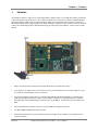
C3PM/C3RM cPCI Pentium M Based Single Board
Computer
User’s Manual
C3RM Manual Rev 1.06
March 17, 2008
Dynatem
23263 Madero, Suite C
Mission Viejo, CA 92691
Phone: (949) 855-3235
Fax: (949) 770-3481
www.dynatem.com
Table of Contents
1.
Features
1
2.
Related Documents
3
3.
Hardware Description
5
3.1
3.2
3.3
3.4
3.5
3.6
3.7
3.8
3.9
4.
Overview
Processor
Chipset
DRAM
Intel 82546EB Dual Gigabit Ethernet Controller
PLX PCI6254 PCI-cPCI Interface
Intel’s FW82802A Firmware Hub Holds the System BIOS In Flash Memory
Clock Drivers
Reset Circuitry
13
Installation
4.1
4.2
4.3
4.4
Dynatem
5
6
6
7
7
8
10
10
11
Installing C3PM in a CompactPCI Chassis
Jumper & GPIO Selectable Options
Discrete I/O vs. COM1 Line Routing
CompactFlash Drive Installation
C3PM cPCI Pentium Processor Board – User’s Manual
13
13
15
16
i
A.
A.1
A.2
B.
B.1
B.2
B.3
Connector Pin-outs
17
CompactFlash Interface Connector (J2 on carrier card)
cPCI Connectors (J1 & J2)
Address Maps, Interrupts, DMA Channels
Memory Map
PCI Configuration Space Map
Interrupt Request Routing
18
19
21
21
21
22
C.
Power and Environmental Requirements
23
D.
X3PMRIO Rear Plug-in I/O Expansion Module
25
ii
C3PM cPCI Pentium Processor Board – User’s Manual
Dynatem
Chapter 1 – Features
1.
Features
The Dynatem C3PM is a single-slot 3U cPCI Single Board Computer (SBC). The C3PM offers full PC performance
with a Pentium M low-power processor. The C3PM is available in two versions: the C3PM for standard industrial
applications and the ANSI/VITA 30.1-2002 compliant, conduction-cooled CRM1 with wedgelocks, stiffener bar,
and a full board heatsink for rugged applications. When referring to attributes of both versions, we will use the name
C3PM. The C3PM employs Intel’s embedded technology to assure long-term availability. Features of the C3PM
include:
•
Single-slot cPCI operation with on-board CompactFlash disk for bootable mass storage.
•
VGA graphics, two USB 2.0 ports, one Serial ATA port, two Fast Ethernet ports, and driven COM1 & 3 ports
are routed out to the backplane via the J2 connector
•
The Intel® 855GME Graphics Memory Controller Hub (GMCH) and Intel® 6300ESB I/O Controller Hub
(ICH) provide high-speed memory control, built-in graphics, integrated I/O including Serial ATA, USB 2.0,
IDE supporting Ultra 100 DMA Mode for transfers up to 88.88 MB/sec, and 64 bit PCI-X bus transfers at 66
MHz
•
Intel’s 82546 Ethernet Controller offers two 10/100/1000BaseTX support routed to J2
•
512 MB of DDR-266 DRAM provided on-board
•
PLX PCI6254 dual mode Universal asynchronous PCI-PCI bridge lets the C3PM act as a peripheral card or
system slot module
Dynatem
C3PM cPCI Pentium Processor Board – User’s Manual
1
Chapter 1 – Features
•
Pigeon Point’s IPM Sentry offers IPMI system management in compliance with PICMG 2.9
•
Primary IDE port for CompactFlash on-board for flash-based mass storage for single-slot booting
•
General Software’s flash-based system BIOS
•
PXE for diskless booting over Ethernet
•
Operating System (OS) and driver support, including Windows NT, Embedded NT, XP, QNX, VxWorks,
Linux, Solaris, and pSOS+
2
C3PM cPCI Pentium Processor Board – User’s Manual
Dynatem
Chapter 2 – Related Documents
2.
Related Documents
Listed below are documents that describe the Pentium processor and chipset, and the peripheral components used on
the C3PM. Either download from the Internet or contact your local distributor for copies of these documents.
The C3PM uses the Low Voltage Pentium M. For information on this processor, go to:
http://www.intel.com/design/intarch/pentiumm/pentiumm.htm
For the ICH component in the 6300ESBchipset get the Intel ® 6300ESB I/O Controller Hub Datasheet. It is document
number 300641-003.
http://www.intel.com/design/intarch/datashts/300641.htm
For the GMCH component in the chipset get the Intel ® 855GM/855GME Chipset Graphics and Memory Controller Hub
(GMCH) Datasheet. It is document number 252615-005:
.
http://www.intel.com/design/chipsets/datashts/252615.htm
For data sheets on I/O controllers:
•
82546EB Fast Ethernet PCI Controller
http://developer.intel.com/design/network/products/lan/controllers/82546.htm
•
CompactPCI Specification PICMG 2.0 R3.0 and other CompactPCI Specifications:
http://www.picmg.org/compactpci.stm#CompactPCISpecifications
•
The PCI-PCI Bridge through which the C3PM accesses the backplane PCI bus is the PCI6254 from PLX:
http://www.plxtech.com/products/fastlane/pci6254.asp
•
Silicon Laboratories CP2102 USB-UART interface device for COM3:
http://www.silabs.com/public/documents/tpub_doc/dsheet/Microcontrollers/Interface/en/cp2102.pdf
The following documents provide information on the PC architecture and I/O:
•
PCI Local Bus Specification, Revision 2.2
http://www.pcisig.com/specifications/
•
PCI-X Specification, Revision 1.0A
http://www.pcisig.com/specifications/
•
System Management Bus Specification (SMBus), Revision 1.1
http://www.smbus.org/specs/
•
Universal Serial Bus Specification
http://www.usb.org/developers
The following documents cover topics relevant to the cPCI and can be purchased through PICMG
http://www.picmg.org/v2internal/specifications.htm:
Dynatem
C3PM cPCI Pentium Processor Board – User’s Manual
3
Chapter 2 – Related Documents
4
C3PM cPCI Pentium Processor Board – User’s Manual
Dynatem
Chapter 3 – Hardware Description
3.
Hardware Description
3.1
Overview
There are presently two revisions of the C3PM, Rev A & Rev B. In this and subsequent chapters, the differences
between the two versions will be described where there are differences.
The block diagram of the C3PM is shown below. The sections that follow describe the major functional blocks of
the C3PM.
Dynatem
C3PM cPCI Pentium Processor Board – User’s Manual
5
Chapter 3 – Hardware Description
3.2
Processor
The C3PM supports a Pentium M processor at 1.4 GHz. The Intel Pentium M processor with 2 MB of L2 cache is
meet the current and future demands of high-performance, low-power embedded computing, making it ideal for
communications, mobile applications, vehicles, and industrial automation applications. While incorporating
advanced processor technology, it remains software-compatible with previous members of the Intel® microprocessor
family.
•
400 MHz front side bus.
•
4 MB of L2 cache for fast large-table look-ups: routing tables.
•
Advanced branch prediction, Micro-op fusion, Hardware stack manager for faster processing.
•
Second-generation Streaming SIMD Extensions (Streaming SIMD Extensions 2) capability adds 144 new
instructions, including 128-bit SIMD integer arithmetic and 128-bit SIMD double-precision floating-point
operation.
•
Fully compatible with existing Intel® Architecture-based software.
For further information on the Pentium M processor available from Intel Corporation, search at:
http://www.intel.com/design/intarch/pentiumm/pentiumm.htm
The Intel® Pentium® M processor was designed from the ground up with a new microarchitecture that delivers high
performance with low power consumption. With its 90 nm processing technology and 2 MB of L2 advanced transfer
cache, the Pentium M offers more performance per Watt.
The Pentium M also offers a dedicated hardware stack manager that employs sophisticated hardware control for
improved stack management, advanced branch prediction capability, and a 400 MHz front side bus to the memory
controller hub.
3.3
Chipset
The Intel® 855GME Graphics Memory Controller Hub (GMCH) and Intel® 6300ESB I/O Controller Hub (ICH)
chipset create an optimized integrated graphics solution with a 400 MHz system bus and integrated 32-bit 3D core at
133 MHz.
The 855GME (GMCH) provides a 266 MHz interface to DDR RAM (72 bits wide with ECC). The C3PM can be
populated with one or two banks of DRAM for 512 MB or 1 GB of total memory respectively. The GMCH system
memory architecture is optimized to maintain open pages (up to 16-kB page size) across multiple rows. As a result,
up to 16 pages across four rows is supported. To complement this, the GMCH will tend to keep pages open within
rows, or will only close a single bank on a page miss.
The 855GME also has an advanced integrated graphical display controller. The C3PM routes its VGA port through
the J2 connector to the system backplane. The X3PMRIO rear plug-in card combines provides a high-density DB-15
connector for the VGA port.
The 6300ESB I/O Controller Hub (ICH) provides most of the C3PM’s on-board I/O and it’s the C3PM’s PCI and
PCI-X expansion bridge. The ICH is designed as a low-power, high-performance I/O hub that features:
•
6
64-bit @ 66 MHz PCI-X expansion that is routed on the C3PM to the 82546 dual channel Fast Ethernet
Controller
C3PM cPCI Pentium Processor Board – User’s Manual
Dynatem
Chapter 3 – Hardware Description
•
32-bit @ 33 MHz PCI bus that supports the PCI6254 PCI/PCI bridge to the backplane
•
Two USB 2.0 compliant ports that are routed to the J2 connector to the backplane and to the optional
X3PMRIO rear I/O module where industry standard USB connectors are provided
•
Integrated IDE controller supports Ultra 100 DMA Mode Transfers for up to 100 MB/sec read cycles and
88.88 MB/sec write cycles for a CompactFlash drive on-board
•
Serial ATA port providing a 150 MB/sec data rate is routed through J2
•
Standard PC functionality like a battery-backed RTC and 256-bytes of CMOS RAM, Power Management
Logic, Interrupt Controller, Watchdog Timer, Integrated 16550 compatible UART’s, and multimedia timers
based on the 82C54
For further information, see the documents referenced in Section 2
3.4
DRAM
The C3PM supports a 72-bit wide, DDR-266 memory interface with memory bandwidth of 2.1 GB/s with ECC. The
module supports 512 MB of DRAM.
3.5
Intel 82546EB Dual Gigabit Ethernet Controller
The C3PM supports two 10/100/1000BaseTX channels accessible from the backplane. The Intel 82546EB Dual
Port Gigabit Ethernet Controller incorporates two full Gigabit Ethernet MAC and PHY layer functions on a single,
compact component. The C3PM uses the PCI-X interface of the ICH to control the 82546EB. Therefore, the front
side data path to the dual Ethernet port controller is 64 bits at 66 MHz.
The Intel 82546EB offers the following features:
•
10, 100, and 1000BaseTX support with auto-negotiation
•
Dual 64KB configurable RX and TX packet FIFOs
•
128-bit internal data path architecture for low latency data handling and superior DMA transfer rate
performance
•
Built-in Phyceiver
•
Serial EEPROM for non-volatile Ethernet address storage
Both 10/100/1000BaseTX ports of the 82546 device are brought out to the J2 backplane connector. Optionally these
two 1 Gb Ethernet ports are brought to industry standard RJ-45 connectors on Dynatem’s rear I/O plug-in module
(X3PMRIO, see Appendix D).
The Intel 82546 contains several PCI configuration registers. It also contains a number of device registers for
controlling the Ethernet operation that can be mapped to the memory space or the I/O space. The PCI signals
specific to the C3PM’s 82546 are shown below:
Dynatem
C3PM cPCI Pentium Processor Board – User’s Manual
7
Chapter 3 – Hardware Description
3.6
Intel 82546 Signal
PCI Bus Connection
Rev A
PCI Bus Connection
Rev B
Bus
IDSEL
PREQ
PGNT
PIRQ for Port A
PIRQ for Port B
2
AD17
PX_REQ0#
PX_GNT0#
PX_IRQ0
PX_IRQ1
2
AD17
PX_REQ0#
PX_GNT0#
PIRQA#
PIRQB#
PLX PCI6254 PCI-cPCI Interface
The PCI-cPCI interface, based on the PLX PCI 6254 on PWB 010 6057 002, offers the following features:
•
64-bit, 33MHz-66MHz Asynchronous operation
•
1 KB FIFO for efficient PCI-PCI bridging and speed conversion.
•
Transparent and non-transparent bridge operation.
•
Usable in the cPCI system slot or a peripheral slot.
The block diagram of the PCI-PCI interface is shown below:
6300ESB
Input/Output
Controller
Hub
COM2
IPMI & Reset
IPMI
Hot Swap Control
PCI @
33 MHz
PCI interface
cPCI P1 Connector
PCI6254
SYSEN# determines system
slot or peripheral operation.
PCI-cPCI Backplane Interface Block Diagram
The is a universal bridge, meaning its mode of operation is determined by the SYSEN# signal on the cPCI
backplane. In this application, the C3PM can be used without jumpers for the system slot or peripheral slot in a
CompactPCI system. The bridge senses the type of slot (system or peripheral) and configures itself as Transparent or
Non-Transparent respectively. In the system slot, the CPU is expected to operate as a host, and the bridge operates
in Transparent mode. In the peripheral slot, the CPU is part of an intelligent subsystem, and the bridge is configured
in Non-Transparent mode so that local resources will not be accessed by the system slot card. Please see the figure
below:
8
C3PM cPCI Pentium Processor Board – User’s Manual
Dynatem
Chapter 3 – Hardware Description
C3PM
6300ESB
ICH
CLK0-6
Transparent
PCI Bridge
PCI
REQ0
GNT0
System Slot
C
o
m
p CLK0-6
a
PCI
c
t
P REQ0
C GNT0
I
b
u
s
C3PM
6300ESB
ICH
Non-Trans
PCI Bridge
Peripheral Slot
This drawing shows how the C3PM operates differently depending on whether it’s in the system slot on the
backplane (denoted by a triangle) or one of the remaining peripheral slots (denoted by circles silkscreened on the
backplane). When in the system slot the six additional REQ/GNT pairs and six additional clocks are routed to the
backplane in compliance with the PICMG CompactPCI spec. These additional CLK and REQ/GNT lines are not
used when the C3PM is installed in a peripheral slot. They are in a tristate mode.
A transparent PCI bridge is meant to provide electrical isolation to the system. It allows additional loads (and
devices) to be attached to the bus, and can also be used to operate dissimilar PCI Bus data widths and speeds on the
same system. For example, a transparent bridge can allow several 32-bit, 33 MHz PCI devices to attach to a 64-bit,
66 MHz PCI-X slot. A non-transparent PCI bridge offers address isolation in addition to electrical isolation.
Devices on both sides of the bridge retain their own independent Memory space, and data from one side of the
bridge is forwarded to the other side, using an address translation mechanism. A non-transparent bridge is used when
there is more than one intelligent entity (such as multiple processors) in the system. It is a common mechanism used
on intelligent I/O cards and in multi-processor systems.
The C3PM reset circuitry is tied to the bridge, since the C3PM can generate the cPCI SYSRESET* signal as well as
be reset by another cPCI board that asserts the SYSRESET* signal. The C3PM reset circuitry is discussed in detail
in Section 3.12.
This section supplements the PCI-to-PCI Bus Bridge documentation (downloadable from PLX Technology’s website
at http://www.plxtech.com/products/fastlane_bridges/default.asp), which contains comprehensive descriptions of the
operation and programming of the PCI 6254.
3.7
Intel’s FW82802AC Firmware Hub Holds the System BIOS In Flash Memory
The Intel FW82802AC uses a 5-pin interface and provides 1 MByte of flash memory for the system BIOS. This
device can fill the 1 MB real mode memory map so only a portion its upper 256 MB is used. The FW82802AC’s 1
MB of memory space is segmented into sixteen parameter blocks of 64 KB each. The C3PM powers up into real
mode and the BIOS is eventually shadowed into system DRAM after booting through the BIOS.
Dynatem
C3PM cPCI Pentium Processor Board – User’s Manual
9
Chapter 3 – Hardware Description
The 6300ESB Southbridge provides the 5-pin interface to the E82802AC. The upper 256 KB of the E82802AC is
located from 000C0000 - 000FFFFF and its full 1 MB of memory is aliased from FFF00000 – FFFFFFFF where it
can be fully accessed after booting up through the BIOS.
Here’s a link to a datasheet for the 82802AC:
ftp://download.intel.com/design/chipsets/datashts/29065804.pdf
3.8
Clock Drivers
The clock driver circuitry is shown below:
Cypress 28409
14.31818 MHz
Crystal
32.768 KHz
Crystal
Pentium M CPU
To ICH for
Real Time
Clock
100 MHz differential
clocks for GMCH,
ICH, ITP, & CPU
clocks
Two 25.0 MHz
Oscillators
ICH
ITP Port
48 MHz
To Ethernet
Controller
82546
To GMCH for SDRAM Clocks
Routed to ICH for
USB and UART’s and
to the GMCH for
Graphics
To ICH for USB & Serial
To GMCH for dot clocks
Clock Driver Circuitry
The clocks are generated by the Cypress CY28409, which is driven by a 14.31818 MHz crystal. DRAM clocks are
synthesized by the GMCH and Hub Interface and PCI(-X) clocks are produced by the ICH. A 32.768 KHz Crystal
drives the Real Time Clock (RTC) on the ICH. The Fast Ethernet port provided to the front panel by the 82541 and
the two 1 Gb Ethernet ports provided to the backplane by the 82546 require separate 25.0 MHz oscillators (one of
the two oscillators is also used for the watchdog timer clock). A 64.0 MHz oscillator drives the PCI 6254cPCI
circuitry.
10
C3PM cPCI Pentium Processor Board – User’s Manual
Dynatem
Chapter 3 – Hardware Description
3.9
Reset Circuitry
The reset circuitry is shown below:
PCI-PCI Bridge to the CompactPCI Backplane
3 Volts
cPCI
SYSRESET
ENUM#
Atmel ATmega 128L IPMI Controller
Optional Reset
Switch
On X3PMRIO
VCSR_SET[RES]
PB1
BD_SEL#
SYSRESET#
Payload Interface
I2C
Payload
Interface
6300ESB ICH
COM2
I2C
PCI Reset
PCI peripherals
SYSRESET#
Reset Control Register
Vcore Monitor
Pentium M “soft” reset
PWRGD_VR
Pentium M “hard” reset
2.5 V Good
Reset Circuitry
Dynatem
C3PM cPCI Pentium Processor Board – User’s Manual
11
Chapter 3 – Hardware Description
There are multiple ways to perform a hard reset of the C3PM:
•
A simple power cycle (turn the chassis’ power off and on).
•
There is an option for using a push button reset: the PRST# signal on the backplane (connector J2, pin C17) that
is generally connected to the chassis’ reset button – the optional X3PMRIO rear plug-in module also provides a
push button for restting through poin C17 of J2
•
When the C3PM is installed in a peripheral slot it can be reset by the system controller module through a
conventional PCI Reset.
•
The PWRGD Circuitry that monitors the on-board power supplies
For further information on the peripherals that play a part in the reset circuitry, refer to ICH datasheet that’s
referenced in Section 2.
12
C3PM cPCI Pentium Processor Board – User’s Manual
Dynatem
Chapter 4 – Installation
4.
Installation
The following sections cover the steps necessary to configure the C3PM and install it into a cPCI system for singleslot operation. This chapter should be read in its entirety before proceeding with the installation.
The C3PM is shipped in an antistatic bag. Be sure to observe proper handling procedures during the configuration
and installation process, to avoid damage due to electrostatic discharge (ESD).
4.1
Installing the C3PM in a CompactPCI Chassis
The C3PM features a Universal PCI-PCI bridge to the backplane. Without changing any jumpers the C3PM will
operate as a system slot card (coming up in transparent mode whereby it can initialize peripheral cards on the
backplane) when installed in the system slot or as a peripheral card in peripheral slots (coming up in non-transparent
mode so that initialization will be done locally without interference from the system slot processor board).
4.2
Jumper & GPIO Selectable Options
The C3PM contains four jumpers for system configuration. The jumpers are indicated in the photo below:
JP4 (3 pins and pin 1
is in a square)
JP2
JP3
82546
GMCH
ICH
DRAM
Bridge
CPU
JP1
Jumpers
Description
JP1
JP2
JP3
JP4
MUST STAY OPEN (left open as the factory default setting)
MUST STAY CLOSED (on-board BIOS is disabled when open)
Used to restore default BIOS settings
COM1 is in RS-232 mode when pins 2&3 are shunted; RS-4xx when pins 1&2
are shunted; GPIO56 is “COM1_TE” and it must be high to enable RS-4xx
Dynatem
C3PM cPCI Pentium Processor Board – User’s Manual
13
Chapter 4 – Installation
Jumper JP1 determines the status of XB_MEM and it should be left open.
XB_MEM (when in the Transparent Mode):
When the C3PM is installed in the System Slot SYS_EN# on the backplane will ground the TRANS# line and put
the module’s 6254 PCI-PCI bridge to the backplane in the transparent mode. XB_MEM will also be grounded as
that signal is connected to TRANS# (and SYS_EN#) through 0 ohm resistor, R338.
XB_MEM(when in the Non-Transparent Mode):
When installed in peripheral slots the C3PM will be in the Non-Transparent mode. When XB_MEM is set to 1, the
PCI 6540 automatically claims 16 MB of Memory space. This allows the boot-up of the Low-Priority Boot port to
proceed without waiting for the Priority Boot port to program the corresponding Memory Base Address registers
(BARs). JP1 must be left open in order for the C3PM to boot in peripheral slots.
Jumper JP3 is used to restore default BIOS settings. It works differently when NV-RAM is battery-backed than
when the settings are stored in a serial EEPROM. When the board uses a battery for holding NV-RAM and RTC
data, close JP3 momentarily (for about 15 seconds when the power is off or the C3PM is out of the chassis) to flush
RTC and NV-RAM and revert to BIOS defaults. The shunt for JP3 should normally be off when a battery is used.
In rugged systems, where no battery is available, JP3 should normally be closed. Follow these steps to change the
stored BIOS settings:
1. Power off the card. Remove JP3, then power on. The BIOS would come up with default setup (read from flash
instead of EEPROM). Hit <DEL> to enter setup. Please note, however, that EEPROM is still in unchanged at this
stage (the BIOS comes up to its "flash" default).
2. Upon entering setup, the BIOS can be modified to preferred configurations or left in default mode. However, the
"save and exit" option MUST be used when exiting the setup menus to write the current setup to the EEPROM.
3. Power off the card. Reinstall JP3. On next power up, the BIOS will read setup parameters from the EEPROM
(which is saved in step #2 above).
COM3 is accessed through USB port 2 through Silicon Laboratories’ CP2102 device since COM2 from the ICH is
used for IPMI. COM3 is configured as RS-232 or RS-4xx by two GPIO lines: GPIO20 & GPIO23. The board will
come up with COM3 undriven so that there won’t be any incompatibility problems with the user device after reset.
GPIO23
GPIO20
(COM3_232EN)
(COM3_422EN)
0 (default)
0
1 (default)
0
1
0
1
1
Mode selected
RS422 driver
Tri-stated
Enabled
RS422
receiver
Tri-stated
Enabled
All off
RS4xx - output
buffer enabled
RS4xx - output
buffer disabled
RS232
RS232
Tri-stated
Tri-stated
Enabled
Tri-stated
Tri-stated
Tri-stated
Tri-Stated
Enabled
To operate in RS-4xx mode, signal COM3_TE (GPIO57) must be high just as COM1_TE (GPIO56) must be high in
order for COM1 to operate in RS-4xx mode. These GPIO lines are routed from the 6300ESB ICH and can be
programmed as described in Intel’s Intel® 6300ESB I/O Controller Hub Datasheet.
14
C3PM cPCI Pentium Processor Board – User’s Manual
Dynatem
Chapter 4 – Installation
4.3
Discrete I/O vs. COM1 Line Routing
The C3PM uses optional 0 ohm resistors to select between discrete I/O and full COM1 support. COM1 RxD and
TxD (in RS-232 mode, RS-4xx mode won’t work as differential pairs are required) are routed directly to the J2
backplane connector but the six additional handshaking lines can alternatively be used for discrete I/O depending on
how these 0 ohm resistors are populated. These resistors CANNOT be modified by the customer without voiding
the warranty unless permission is granted by Dynatem, (800)543-3830.
The photo below shows the solder side of the C3PM and the yellow, dashed box indicates these 0 ohm optional
resistors. The drawing to the right of the photo corresponds to the resistor layout in the yellow box. Green resistors
route COM1 lines and goldenrod resistors route GPIO lines when populated. The optional resistors are horizontal to
each other: either R251 is populated or R52; R247 is populated or R248…etc. The factory default option is to
populate the goldenrod resistors for full GPIO support. Not all lines must be used for COM1 or for GPIO and the
following table indicates the functionality routed by the various resistors.
Dynatem
C3PM cPCI Pentium Processor Board – User’s Manual
R251
R252
R247
R248
R223
R224
R218
R219
R211
R212
R210
R213
15
Chapter 4 – Installation
Resistor
R251
R247
R223
R218
R211
R210
4.4
COM1 RS-232
RTS
CTS
-
COM1 RS-4xx
CTSTxDRTS+
CTS+
RxDRTS-
Resistor
R252
R248
R224
R219
R212
R213
GPIO Line
GPIO41
GPIO28
GPIO37
GPIO40
GPIO39
GPIO38
CompactFlash Drive Installation
The C3PM supports a bootable CompactFlash Drive for single-slot booting. Connector J2 is a Type I CompactFlash
connector with a retention clip for rugged applications and is used for this purpose. J2 is located on a special
CompactFlash carrier module that bolts to the top side cooling plate/heat sink so that the drive will be accessible.
Use a screwdriver to release the clip. The CompactFlash module must be unbolted and removed before the CF drive
can be replaced or removed.
16
C3PM cPCI Pentium Processor Board – User’s Manual
Dynatem
Appendix A – Connector Pin-outs
A.
Connector Pin-outs
The locations of the C3PM connectors are shown below.
J2
J1
J6: CompactFlash
Dynatem
C3PM cPCI Pentium Processor Board – User’s Manual
17
Appendix A – Connector Pin-outs
A.1
Pin
CompactFlash Interface Connector
Signal
Pin
Signal
1
GND
26
CMPFLASHDET
2
D3
27
D11
3
D4
28
D12
4
D5
29
D13
5
D6
30
D14
6
D7
31
D15
7
CS1#
32
CS3#
8
GND
33
No connection
9
GND
34
DIOR#
10
GND
35
DIOW#
11
GND
36
+5 VDC
12
GND
37
DIRQ (IRQ15)
13
+5 VDC
38
+5 VDC
14
GND
39
Pulled Low (master)
15
GND
40
No connection
16
GND
41
IDERESET
17
GND
42
Pulled Up (DIORDY)
18
DA2
43
No connection
19
DA1
44
+5 VDC
20
DA0
45
No connection
21
D0
46
Pull-up to +5 VDC
22
D1
47
D8
23
D2
48
D9
24
No connection
49
D10
25
No connection
50
GND
CompactFlash Type II Interface Connector (J2 on CF carrier)
18
C3PM cPCI Pentium Processor Board – User’s Manual
Dynatem
Appendix A – Connector Pin-outs
A.2
cPCI Connectors (J1 & J2)
Connector J2 brings a 32-bit 33 MHz capable PCI bus to the CompactPCI backplane. “PU” stands for “pulled up”.
As was described in Chapter 4, some pins can be used for GPIO lines (in red font) or for COM1 signals. Signal
names in blue italics were changed for C3RM Manual Rev 105, February 1, 2008.
Pin
Signal
Pin
Signal
Pin
Signal
Pin
Signal
Pin
Signal
A22
A21
A20
A19
A18
A17
A16
A15
A14
A13
A12
A11
A10
A09
A08
A07
A06
A05
A04
A03
A02
A01
GA4
CLK6
CLK5
GND
COM3_TXDCOM3_TXD+
COM3_RTSCOM3_RTS+
COM3_RXD+
COM3_RXDCOM3_CTS+
COM3_CTSVGA_VCC
VGA_HSYNC
VGA_VSYNC
VGA_DDCD
VGA_DDCC
VGA Ground
VI/O
CLK4
CLK2
CLK1
B22
B21
B20
B19
B18
B17
B16
B15
B14
B13
B12
B11
B10
B09
B08
B07
B06
B05
B04
B03
B02
B01
GA3
GND
GND
GND
COM1_TXDGND
COM1_RXD+
GND
USB0_GND
GND
USB0_D+
GND
USB1_D+
GND
USB1_GND
GND
SATA0_TX+
GND
SATA0_RX+
GND
CLK3
GND
C22
C21
C20
C19
C18
C17
C16
C15
C14
C13
C12
C11
C10
C09
C08
C07
C06
C05
C04
C03
C02
C01
GA2
ETH0_DC+
ETH0_DCETH0_DD+
ETH0_DDPRST#
DEG#(Pulled up)
FAL#(Pulled up)
USB0_VCC
VI/O
USB0_DVI/O
USB1_DVI/O
USB1_VCC
VI/O
SATA0_TXVI/O
SATA0_RXGNT3#
SYSEN#
REQ1#
D22
D21
D20
D19
D18
D17
D16
D15
D14
D13
D12
D11
D10
D09
D08
D07
D06
D05
D04
D03
D02
D01
GA1
BIT_PASS#
GND
BIOS_WP#
GND
REQ6#
GND
REQ5#
E22
E21
E20
E19
E18
E17
E16
E15
E14
E13
E12
E11
E10
E09
E08
E07
E06
E05
E04
E03
E02
E01
GA0
ETH0_DA+
ETH0_DAETH0_DB+
ETH0_DBGNT6#
VBATT
GNT5#
ETH1_DA+
ETH1_DAETH1_DB+
ETH1_DBETH1_DC+
ETH1_DCETH1_DD+
ETH1_DDGPIO43
VGA_Green
VGA_Blue
GNT4#
REQ3#
REQ2#
COM1_TXD+/28
COM1_RTS-/37
GND
COM1_RTS+/38
COM1_RXD-/39
COM1_CTS+/40
GND
COM1_CTS-/41
GPIO42
VGA_Red
GND
REQ4#
GNT2#
GNT1#
CompactPCI Backplane Connector (J2) – Row F is grounded
RS-232 Signals
RS-4xx Signals
Clear To Send (CTS) Input
Received Data (RxD) Input
Transmitted Data (TxD) Output
Request To Send (RTS) Output
-
TxDRTSCTS+
RxD+
TxD+
RTS+
CTSRxD-
Conversion between RS-232 and RS-4xx ports (applies to both COM1 & COM3 (RS-4xx negative (-)
lines are not used when in the RS232 mode))
Dynatem
C3PM cPCI Pentium Processor Board – User’s Manual
19
Appendix A – Connector Pin-outs
Connector J1 brings a 32-bit 33 MHz capable PCI bus to the CompactPCI backplane. “PU” stands for “pulled up”.
Pin
Signal
Pin
Signal
Pin
Signal
Pin
Signal
Pin
Signal
A25
A24
A23
A22
A21
A20
A19
A18
A17
A16
A15
A14
A13
A12
A11
A10
A09
A08
A07
A06
A05
A04
A03
A02
A01
5 VDC
AD1
3.3 VDC
AD7
3.3 VDC
AD12
3.3 VDC
SERR#
3.3 VDC
DEVSEL#
3.3 VDC
B25
B24
B23
B22
B21
B20
B19
B18
B17
B16
B15
B14
B13
B12
B11
B10
B09
B08
B07
B06
B05
B04
B03
B02
B01
REQ64#
5 VDC
AD4
GND
AD9
GND
AD15
GND
IPMB_SCL
GND
FRAME#
C25
C24
C23
C22
C21
C20
C19
C18
C17
C16
C15
C14
C13
C12
C11
C10
C09
C08
C07
C06
C05
C04
C03
C02
C01
ENUM#
VIO
AD3
3.3 VDC
AD8
VIO
AD14
3.3 VDC
IPMB_SDA
VIO
IRDY#
D25
D24
D23
D22
D21
D20
D19
D18
D17
D16
D15
D14
D13
D12
D11
D10
D09
D08
D07
D06
D05
D04
D03
D02
D01
3.3 VDC
AD0
5 VDC
AD6
M66EN
AD11
GND
PAR
GND
STOP#
BD_SEL#
E25
E24
E23
E22
E21
E20
E19
E18
E17
E16
E15
E14
E13
E12
E11
E10
E09
E08
E07
E06
E05
E04
E03
E02
E01
5 VDC
ACK64#
AD2
AD5
C/BE0#
AD10
AD13
C/BE1#
PERR#
LOCK#
TRDY#
KEY
AD18
AD21
C/BE3#
AD26
AD30
REQ0#
RSVD
IPMB_PWR
INTA#
TCK
5 VDC
KEY
AD17
GND
IDSEL
GND
AD29
PCI_Present#
RSVD
HEALTHY#
INTB#
5 VDC
-12 VDC
KEY
AD16
3.3 VDC
AD23
VIO
AD28
3.3 VDC
RST#
VIO
INTC#
TMS
TRST#
KEY
GND
AD20
GND
AD25
GND
CLK0
GND
INTP
5 VDC
TDO
+12 VDC
KEY
C/BE2#
AD19
AD22
AD24
AD27
AD31
GNT0#
INTS
INTD#
TDI
5 VDC
CompactPCI Backplane Connector (J1) – Row F is grounded
20
C3PM cPCI Pentium Processor Board – User’s Manual
Dynatem
Appendix B – Address Maps, Interrupts, DMA Channels
B.
Address Maps, Interrupts, DMA Channels
Tables of the C3PM’s address maps, interrupt request assignments, and DMA channel usage are given in the
following sections. All addresses are shown in hexadecimal notation.
B.1
Memory Map
The C3PM’s memory map is shown below:
Address Range
Description
00000000 – 000FFFFF
00100000 – 1FFFFFFF
80000000 – BFFFFFFF
C0000000 - FBFFFFFF
FC000000 - FFFFFFFF
FFE00000 - FFFFFFFF
DOS legacy address range
On-board DDR DRAM 512 MB
Prefetchable PCI Device Allocation
Non-prefetchable PCI Device Allocation
reserved for Mother board Resources
High BIOS Area
This is the memory map on the chipset..
For further details on the C3PM memory space map, refer to Section 5.1 in Intel’s 855GM/855GME Chipset
Graphics and Memory Controller Hub(GMCH) Datasheet, Document # 252615-004, available from Intel
Corporation.
B.2
PCI Configuration Space Map
The PCI configuration space map will vary if the PMCX expansion slot is used to support a PMCX add-on
mezzanine card and if that PMCX module uses a expansion bridge designed for multiple targets on the secondary
bus. This is an extremely unlikely situation but the bus numbers in this condition will differ from those provided in
the following table. The Vendor ID and Device ID in hex for the PMCX slot are shown as xxxx, since they depend
on the type of device installed in the PMC slot.
IDSEL
Bus
Dev
Fcn
VenID
—
—
—
—
—
—
—
—
AD17
AD17
AD19
Slot #
00
00
00
00
00
00
00
00
01
01
01
02
28
31
31
31
31
29
29
29
1
3
3
xx
0
0
1
2
3
0
1
5
0
1
0
xx
8086
8086
8086
8086
8086
8086
8086
8086
8086
8086
3388
xxxx
Dynatem
DevID
Description
25AE 6300ESB (ICH) bridge to PCIX bus (for dual Enet)
25A1
6300ESB (ICH) P2L Bridge
25A2
6300ESB (ICH) PCI-IDE Interface
25A3
6300ESB (ICH) SATA Interface
25A4
6300ESB (ICH) SMBus Interface
25A9
6300ESB (ICH) PCI-USB#0 Interface
25AA 6300ESB (ICH) PCI-USB#1 Interface
25AC 6300ESB (ICH) APIC
1010
82546 Gb Ethernet Channel #1
1010
82546 Gb Ethernet Channel #2
0020
PCI 6254 bridge to CPCI bus
xxxx
CPCI device
PCI Configuration
C3PM cPCI Pentium Processor Board – User’s Manual
21
Appendix B – Address Maps, Interrupts, DMA Channels
B.3
Interrupt Request Routing
The ISA interrupt request routing is shown below:
IRQ
0
1
2
3
4
5
6
*7
8
9
10
11
12
13
14
Description
Timer 0 (ICH)
Cascade Interrupt from slave PIC (ICH)
COM2
COM1
Parallel Port
Real Time Clock (ICH)
82546 Gb Ethernet
USB#1
USB#0
Math Coprocessor (ICH)
Primary IDE Interface (CompactFlash) (ICH)
The PCI interrupt request routing of additional interrupts (all IRQs are routed to the 6300ESB ICH) :
PIIX4 PCI IRQ
Rev 001 C3PM
Rev 002 C3PM
PCI6254 Bridge IRQ
82546EB INT#A
82546EB INT#B
*INTA#, J1.A3
*INTB#, J1.B3
*INTC#, J1.C3
*INTD#, J1.E3
PXIRQ0#
PXIRQ1#
PXIRQ0#
PXIRQ1#
PXIRQ2#
PXIRQ3#
PIRQE# (optional)
PIRQA#
PIRQB#
PIRQE#
PIRQF#
PIRQG#
PIRQH#
*These are IRQs routed from J1 on the CompactPCI backplane.
Rev 001 versions of the module use a flex cable connection to the CompactFlash sub-assembly or can be identified
by “PWB D010-6062-001” being etched into the PCB on the solder side, near the front edge.
For further details on interrupts, refer to the documentation for the various peripherals that generate interrupts, as
well as Intel 6300ESB I/O Controller Hub Datasheet, Document #300641-002.
22
C3PM cPCI Pentium Processor Board – User’s Manual
Dynatem
Appendix C – Power and Environmental Requirements
C.
Power and Environmental Requirements
The C3PM power and environmental requirements are shown in the tables below.
Condition
Power Requirements
1.4 MHz Pentium M
5 VDC @ 3.4 A max, 3.3 VDC @ 2.2 A
max
3.0 VDC Lithium Coin Cell @ 3.4 μA
Power Requirements
The 3 Volt lithium coin cell is a CR2032 with 190 mAhours capacity and it is used to battery-back the Real Time
Clock, the 2 MB of NV-SRAM, and the BIOS’s NV-RAM. At 3.4 μA this battery should last for over six years with
power off.
Condition
Environmental Requirements
Operating Temperature
-40° to +71° C (can be screened for -40°
to 85° C)
-50° to +105° C
Storage Temperature
Environmental Requirements
Dynatem
C3PM cPCI Pentium Processor Board – User’s Manual
23
Appendix C – Power and Environmental Requirements
24
C3PM cPCI Pentium Processor Board – User’s Manual
Dynatem
Appendix D – X3PMRIO Rear Plug-in I/O Expansion Module for the C3PM
D.
X3PMRIO Rear Plug-in I/O Expansion Module for the C3PM
All of the C3PM’s I/O is routed directly through the J2 connector so a rear plug-in module is useful for interfacing to
industry standard cables. The X3PMRIO is available for this purpose. Here is a photo of the X3PMRIO:
J7: SATA0
PB1: Reset Button
J4: LANa
J3: LANb
J2: SVGA
J1: USB0 & USB1
BT1: Battery
(a CR2032)
J6: COM1
J5: COM3
Shunting JP1 grounds GPIO42. Shunting JP2 grounds GPIO43. Shunting JP3 write protects the BIOS on the
C3PM. Shunting JP4 grounds GPIO24 (AKA BIT_PASS#).
Pin-outs for the X3PMRIO’s connectors are found on the following pages.
Dynatem
C3PM cPCI Pentium Processor Board – User’s Manual
25
Appendix D – C3PMPTB Rear Plug-in I/O Expansion Module for the C3PM
Signal names in blue italics were changed for C3RM Manual Rev 105, February 1, 2008.
Pin
COM1 RS-232 (RP5 Installed)
COM1 RS-4xx (RP4 &
RP6 Installed)
1
2
3
4
5
6
7
8
9
Received Data (RxD) Input
Transmitted Data (TxD) Output
GND
Request to Send (RTS) Output
Clear To Send (CTS) Input
-
+TxD
+RTS
+CTS
+RxD
GND
-TxD
-RTS
-CTS
-RxD
COM1 Connector (J6) – DB9M Connector. The metal shell of the connector goes to chassis
ground.
Pin
COM3 RS-232 (RP2 Installed)
COM3 RS-4xx (RP1 &
RP3 Installed)
1
2
3
4
5
6
7
8
9
Received Data (RxD) Input
Transmitted Data (TxD) Output
GND
Request to Send (RTS) Output
Clear To Send (CTS) Input
-
+TxD
+RTS
+CTS
+RxD
GND
-TxD
-RTS
-CTS
-RxD
COM3 Connector (J5) – DB9M Connector. The metal shell of the connector goes to chassis
ground.
Pin
Signal
1
2
3
4
5
6
7
GND
TxD+
TxDGND
RxDRxD+
GND
Serial ATA, SATA 0, Connector (J7)
26
C3PM cPCI Pentium Processor Board – User’s Manual
Dynatem
Appendix D – X3PMRIO Rear Plug-in I/O Expansion Module for the C3PM
J4
Pin
10/100 Signal Description
Gb Signal Description
A1
A2
A3
A4
A5
A6
A7
A8
Port A Transmit Data + (TX+)
TP0+
A Transmit Data - (TX-)
TP0-
A Receive Data + (RX+)
TP1+
Unused
TP2+
Unused
TP2-
A Receive Data - (RX-)
TP1-
Unused
TP3+
Unused
TP3-
J3
Pin
10/100 Signal Description
Gb Signal Description
B1
B2
B3
B4
B5
B6
B7
B8
Port B Transmit Data + (TX+)
TP0+
B Transmit Data - (TX-)
TP0-
B Receive Data + (RX+)
TP1+
Unused
TP2+
Unused
TP2-
B Receive Data - (RX-)
TP1-
Unused
TP3+
Unused
TP3-
10BaseT/100BaseTX Fast Ethernet Connector (J4/J3) –RJ-45 Connectors.
Pin
Signal
1
2
3
4
5
6
7
8
9
10
11
12
USB Vcc
USB Port 0 Negative
USB Port 0 Positive
GND
USB Vcc
USB Port 1 Negative
USB Port 1 Positive
GND
Chassis GND
Chassis GND
Chassis GND
Chassis GND
Dual Port USB 2.0 Connector (J1)
Dynatem
C3PM cPCI Pentium Processor Board – User’s Manual
27
Appendix D – C3PMPTB Rear Plug-in I/O Expansion Module for the C3PM
Pin
1
2
3
4
5
6
7
8
9
10
11
12
13
14
15
Signal Description
Red Output
Green Output
Blue Output
No connection
HSYNC/VSYNC Return (GND)
Red Return (GND)
Green Return (GND)
Blue Return (GND)
+5 VDC
HSYNC/VSYNC Return (GND)
No connection
DDCDAT
Horizontal Sync (HSYNC) Output
Vertical Sync (VSYNC) Output
DDCCLK
VGA Connector (J2) –DB15F Connector. The metal shell of the connector goes to chassis ground.
28
C3PM cPCI Pentium Processor Board – User’s Manual
Dynatem