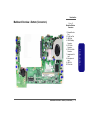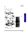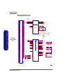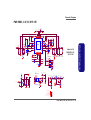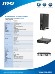
1
Preface Notebook Computer M1110Q/M1110Q-C Service Manual Preface I Preface Notice The company reserves the right to revise this publication or to change its contents without notice. Information contained herein is for reference only and does not constitute a commitment on the part of the manufacturer or any subsequent vendor. They assume no responsibility or liability for any errors or inaccuracies that may appear in this publication nor are they in anyway responsible for any loss or damage resulting from the use (or misuse) of this publication. This publication and any accompanying software may not, in whole or in part, be reproduced, translated, transmitted or reduced to any machine readable form without prior consent from the vendor, manufacturer or creators of this publication, except for copies kept by the user for backup purposes. Preface Brand and product names mentioned in this publication may or may not be copyrights and/or registered trademarks of their respective companies. They are mentioned for identification purposes only and are not intended as an endorsement of that product or its manufacturer. Version 1.0 July 2010 Trademarks Intel and Intel Atom are trademarks of Intel Corporation. Windows® is a registered trademark of Microsoft Corporation. Other brand and product names are trademarks and /or registered trademarks of their respective companies. II Preface About this Manual This manual is intended for service personnel who have completed sufficient training to undertake the maintenance and inspection of personal computers. It is organized to allow you to look up basic information for servicing and/or upgrading components of the M1110Q/ M1110Q-C series notebook PC. The following information is included: Chapter 1, Introduction, provides general information about the location of system elements and their specifications. Chapter 2, Disassembly, provides step-by-step instructions for disassembling parts and subsystems and how to upgrade elements of the system. Preface Appendix A, Part Lists Appendix B, Schematic Diagrams Appendix C, Updating the FLASH ROM BIOS III Preface IMPORTANT SAFETY INSTRUCTIONS Follow basic safety precautions, including those listed below, to reduce the risk of fire, electric shock and injury to persons when using any electrical equipment: Preface 1. Do not use this product near water, for example near a bath tub, wash bowl, kitchen sink or laundry tub, in a wet basement or near a swimming pool. 2. Avoid using a telephone (other than a cordless type) during an electrical storm. There may be a remote risk of electrical shock from lightning. 3. Do not use the telephone to report a gas leak in the vicinity of the leak. 4. Use only the power cord and batteries indicated in this manual. Do not dispose of batteries in a fire. They may explode. Check with local codes for possible special disposal instructions. 5. This product is intended to be supplied by a Listed Power Unit with an AC Input of 100 - 240V, 50 - 60Hz, DC Output of 19V, 1.58A (30W) minimum AC/DC Adapter. IV Preface Instructions for Care and Operation The notebook computer is quite rugged, but it can be damaged. To prevent this, follow these suggestions: 1. Don’t drop it, or expose it to shock. If the computer falls, the case and the components could be damaged. Do not expose the computer to any shock or vibration. 2. Do not place anything heavy on the computer. Keep it dry, and don’t overheat it. Keep the computer and power supply away from any kind of heating element. This is an electrical appliance. If water or any other liquid gets into it, the computer could be badly damaged. Do not leave it in a place where foreign matter or moisture may affect the system. Don’t use or store the computer in a humid environment. Do not place the computer on any surface which will block the vents. Preface Do not expose it to excessive heat or direct sunlight. 3. Do not place it on an unstable surface. Follow the proper working procedures for the computer. Shut the computer down properly and don’t forget to save your work. Remember to periodically save your data as data may be lost if the battery is depleted. Do not turn off the power until you properly shut down all programs. Do not turn off any peripheral devices when the computer is on. Do not disassemble the computer by yourself. Perform routine maintenance on your computer. V Preface 4. 5. Avoid interference. Keep the computer away from high capacity transformers, electric motors, and other strong magnetic fields. These can hinder proper performance and damage your data. Take care when using peripheral devices. Use only approved brands of peripherals. Unplug the power cord before attaching peripheral devices. Preface Power Safety The computer has specific power requirements: VI • • Power Safety Warning • Before you undertake any upgrade procedures, make sure that you have turned off the power, and disconnected all peripherals and cables (including telephone lines). It is advisable to also remove your battery in order to prevent accidentally turning the machine on. • • • Only use a power adapter approved for use with this computer. Your AC adapter may be designed for international travel but it still requires a steady, uninterrupted power supply. If you are unsure of your local power specifications, consult your service representative or local power company. The power adapter may have either a 2-prong or a 3-prong grounded plug. The third prong is an important safety feature; do not defeat its purpose. If you do not have access to a compatible outlet, have a qualified electrician install one. When you want to unplug the power cord, be sure to disconnect it by the plug head, not by its wire. Make sure the socket and any extension cord(s) you use can support the total current load of all the connected devices. Before cleaning the computer, make sure it is disconnected from any external power supplies. Do not plug in the power cord if you are wet. Do not use the power cord if it is broken. Do not place heavy objects on the power cord. Preface Battery Precautions • Only use batteries designed for this computer. The wrong battery type may explode, leak or damage the computer. • Do not continue to use a battery that has been dropped, or that appears damaged (e.g. bent or twisted) in any way. Even if the computer continues to work with a damaged battery in place, it may cause circuit damage, which may possibly result in fire. • Recharge the batteries using the notebook’s system. Incorrect recharging may make the battery explode. • Do not try to repair a battery pack. Refer any battery pack repair or replacement to your service representative or qualified service personnel. • Keep children away from, and promptly dispose of a damaged battery. Always dispose of batteries carefully. Batteries may explode or leak if exposed to fire, or improperly handled or discarded. • Keep the battery away from metal appliances. • Affix tape to the battery contacts before disposing of the battery. • Do not touch the battery contacts with your hands or metal objects. Battery Guidelines Preface The following can also apply to any backup batteries you may have. • If you do not use the battery for an extended period, then remove the battery from the computer for storage. • Before removing the battery for storage charge it to 60% - 70%. • Check stored batteries at least every 3 months and charge them to 60% - 70%. Battery Disposal The product that you have purchased contains a rechargeable battery. The battery is recyclable. At the end of its useful life, under various state and local laws, it may be illegal to dispose of this battery into the municipal waste stream. Check with your local solid waste officials for details in your area for recycling options or proper disposal. Caution Danger of explosion if battery is incorrectly replaced. Replace only with the same or equivalent type recommended by the manufacturer. Discard used battery according to the manufacturer’s instructions. Battery Level Click the battery icon in the taskbar to see the current battery level and charge status. A battery that drops below a level of 10% will not allow the computer to boot up. Make sure that any battery that drops below 10% is recharged within one week. VII Preface Related Documents You may also need to consult the following manual for additional information: User’s Manual on DVD This describes the notebook PC’s features and the procedures for operating the computer and its ROM-based setup program. It also describes the installation and operation of the utility programs provided with the notebook PC. System Startup Preface 1. Remove all packing materials. 2. Place the computer on a stable surface. 3. Securely attach any peripherals you want to use with the computer (e.g. keyboard and mouse) to their ports. 4. Attach the AC/DC adapter to the DC-In jack on the left of the computer, then plug the AC power cord into an outlet, and connect the AC power cord to the AC/DC adapter. 5. Use one hand to raise the lid/LCD to a comfortable viewing angle (do not exceed 120 degrees); use the other hand (as illustrated in <Hyperlink B n I>Figure 1) to support the base of the computer (Note: Never lift the computer by the lid/LCD). 6. Press the power button to turn the computer “on”. VIII Figure 1 - Opening the Lid/LCD/Computer with AC/DC Adapter Plugged-In Preface Contents Schematic Diagrams................................. B-1 Overview .........................................................................................1-1 Specifications ..................................................................................1-2 External Locator - Top View with LCD Panel Open ......................1-4 External Locator - Front & Right Side Views .................................1-5 External Locator - Left Side & Rear View .....................................1-6 External Locator - Bottom View .....................................................1-7 Mainboard Overview - Top (Key Parts) .........................................1-8 Mainboard Overview - Bottom (Key Parts) ....................................1-9 Mainboard Overview - Top (Connectors) .....................................1-10 Mainboard Overview - Bottom (Connectors) ...............................1-11 System Block Diagram ...................................................................B-2 Pineview CPU Part-D .....................................................................B-3 Pineview CPU Part A-C-F ..............................................................B-4 Pineview CPU Part B ......................................................................B-5 Pineview CPU Part E ......................................................................B-6 DDRIII SO-DIMM_0 .....................................................................B-7 Clock Generator ..............................................................................B-8 Tigerpoint Part A-B ........................................................................B-9 Tigerpoint Part C .........................................................................B-10 Tigerpoint Part D ..........................................................................B-11 Tigerpoint Part E-F .......................................................................B-12 USB, Panel, HDD, LED ...............................................................B-13 BTB, 3G, WLAN, BT ...................................................................B-14 Audio Codec VT1812 ...................................................................B-15 KBC-ITE IT8502E-J, TP, LID .....................................................B-16 PWR AC_IN, Charge ...................................................................B-17 PWR SW, 1.8VS, 3VS, 5VS, 1.5VS ............................................B-18 PWR VDD3, 3.3V, 5V, SYS 15V ................................................B-19 PWR 1.5V, 0.75V .........................................................................B-20 PWR 0.89V, 1.05VS, 1.5VS .........................................................B-21 PWR VCORE ...............................................................................B-22 CRT ...............................................................................................B-23 Card Reader (with LAN) JMB261 ................................................B-24 BTB, USB, CCD, PWR SW .........................................................B-25 Click Board ...................................................................................B-26 Power Button Board .....................................................................B-27 Disassembly ...............................................2-1 Overview .........................................................................................2-1 Maintenance Tools ..........................................................................2-2 Connections .....................................................................................2-2 Maintenance Precautions .................................................................2-3 Disassembly Steps ...........................................................................2-4 Removing the Battery ......................................................................2-5 Removing the System Memory (RAM) ..........................................2-6 Removing the Wireless LAN Module .............................................2-8 Removing the Keyboard ..................................................................2-9 Removing the Hard Disk Drive .....................................................2-10 Removing the Bluetooth Module ..................................................2-12 Part Lists ..................................................A-1 Parts List Illustration Location ....................................................... A-2 Top ................................................................................................. A-3 Bottom ............................................................................................ A-4 LCD ................................................................................................ A-5 Updating the FLASH ROM BIOS......... C-1 To update the FLASH ROM BIOS you must: C-1 IX Preface Introduction ..............................................1-1 Preface Preface Download the BIOS ....................................................................... C-1 Unzip the downloaded files to a bootable CD/DVD/ or USB Flash drive ................................................................................................ C-1 Set the computer to boot from the external drive ........................... C-1 Use the flash tools to update the BIOS .......................................... C-2 Restart the computer (booting from the HDD) .............................. C-2 X Introduction Chapter 1: Introduction Overview This manual covers the information you need to service or upgrade the M1110Q/M1110Q-C series notebook computer. Information about operating the computer (e.g. getting started, and the Setup utility) is in the User’s Manual. Information about dri-vers (e.g. VGA & audio) is also found in the User’s Manual. The manual is shipped with the computer. Operating system Window 7 has its own manuals as do application softwares (e.g. word processing and database programs). If you have questions about those programs, you should consult those manuals. 1.Introduction The M1110Q/M1110Q-C series notebook is designed to be upgradeable. See Disassembly on page 2 - 1 for a detailed description of the upgrade procedures for each specific component. Please take note of the warning and safety information indicated by the “” symbol. The balance of this chapter reviews the computer’s technical specifications and features. Overview 1 - 1 Introduction Specifications Latest Specification Information 1.Introduction The specifications listed here are correct at the time of sending them to the press. Certain items (particularly processor types/speeds) may be changed, delayed or updated due to the manufacturer's release schedule. Check with your service center for more details. Processor Security Intel® Atom™ Processor N455 1.66GHz, 512KB L2 Cache, 667MHz FSB, TDP:6.5W Kensington Lock Slot BIOS Password Intel® Atom™ Processor N475 1.83GHz, 512KB L2 Cache, 667MHz FSB, TDP:6.5W Interface Intel® NM10 Express Chipset Three USB 2.0 Ports One Headphone-Out Jack One Microphone-In Jack One External Monitor Port One RJ-45 LAN Jack One DC-in Jack Memory Keyboard One 204 Pin SO-DIMM Socket Supporting DDR3 667MHz Memory “WinKey” keyboard (with embedded numeric keypad) Display 10.1” (25,6cm) WSVGA TFT LCD Core Logic Memory Expandable up to 2GB CPU Video Adapter The CPU is not a user serviceable part. Accessing the CPU in any way may violate your warranty. Intel GMA 3150 Shared Memory Architecture (DVMT) up to 384MB MS DirectX® 9.0 compatible Storage One Changeable 2.5" 9.5mm (h) SATA Hard Disk Drive (Factory Option) External USB DVD Super Multi Drive Module BIOS One 8Mb SPI Flash ROM Phoenix™ BIOS Audio High Definition Audio Compliant Interface 2 * Built-In Speakers Built-In Microphone 1 - 2 Specifications Pointing Device Built-in Touchpad Communication 10Mb/100Mb Ethernet LAN 300K Pixel USB PC Camera Module (Factory Option) Bluetooth 2.1 + EDR Module (Factory Option) 3.75G/HSPA Half Mini-Card Module (Factory Option) 802.11b/g/n Wireless LAN Half Mini-Card Module Card Reader Embedded 8-in-1 Card Reader MMC (MultiMedia Card) / RS MMC SD (Secure Digital) / Mini SD / SDHC MS (Memory Stick) / MS Pro / MS Duo Introduction Power Full Range AC/DC Adapter AC Input: 100 - 240V, 50 - 60Hz DC Output: 19V, 1.58A (30W) Removable 3 Cell Smart Lithium-Ion Battery Pack, 24.42WH (Factory Option) Removable 6 Cell Smart Lithium-Ion Battery Pack, 48.84WH Energy Star 5.0 Compliant Environmental Spec 1.Introduction Temperature Operating: 5°C - 35°C Non-Operating: -20°C - 60°C Relative Humidity Operating: 20% - 80% Non-Operating: 10% - 90% Dimensions & Weight Model A: 266mm (w) x 185mm (d) x 18.5 - 25.4mm (h) 0.94kg (with 24.42WH Battery) Model B: 266mm (w) x 185mm (d) x 18.5 - 26.6mm (h) 0.97kg (with 24.42WH Battery) Model C: 266mm (w) x 185mm (d) x 19.7 - 27.1mm (h) 0.93kg (with 24.42WH Battery) Specifications 1 - 3 Introduction Figure 1 External Locator - Top View with LCD Panel Open 1.Introduction Top View 1 1. Built-In PC Camera 2. LCD 3. Keyboard 4. Built-In Microphone 5. Touchpad & Buttons 6. LED Indicators 2 3 4 6 1 - 4 External Locator - Top View with LCD Panel Open 5 Introduction External Locator - Front & Right Side Views Figure 2 Front View 1. LED Indicators FRONT VIEW 1 Right Side View RIGHT SIDE VIEW 5 1 2 2 3 1. 8-in-1 Card Reader 2. 2 * USB 2.0 Ports 3. RJ-45 LAN Port 4. External Monitor Port 5. Power Button 4 External Locator - Front & Right Side Views 1 - 5 1.Introduction Figure 3 Introduction External Locator - Left Side & Rear View Figure 4 Left Side View Security Lock Slot DC-In Jack Vent USB 2.0 Port Microphone-In Jack 6. Headphone-Out Jack / LEFT SIDE VIEW 1 2 3 4 1.Introduction 1. 2. 3. 4. 5. Figure 5 Rear View 1. Battery REAR VIEW 1 1 - 6 External Locator - Left Side & Rear View 5 6 Introduction External Locator - Bottom View Figure 6 Bottom View 1. Battery 2. Component Bay Cover 3. Vent 4. Speakers 1 1.Introduction 3 2 Overheating 4 4 To prevent your computer from overheating, make sure nothing blocks any vent while the computer is in use. External Locator - Bottom View 1 - 7 Introduction Figure 7 Mainboard Overview - Top (Key Parts) Mainboard Top Key Parts Clock Generator Azalia Codec KBC-ITE IT8502E JMC261 8-in-1 Card Reader Socket 1.Introduction 1. 2. 3. 4. 5. 1 2 3 4 1 - 8 Mainboard Overview - Top (Key Parts) 5 Introduction Mainboard Overview - Bottom (Key Parts) Figure 8 Mainboard Bottom Key Parts 5 4 3 1 2 Mainboard Overview - Bottom (Key Parts) 1 - 9 1.Introduction 1. Mini-Card Connector (WLAN Module) 2. Optional Mini-Card Connector (3.5G Module) 3. Memory Slot DDR3 SO-DIMM 4. South Bridge 5. Embedded CPU Introduction Figure 9 Mainboard Overview - Top (Connectors) 1.Introduction Mainboard Top Connectors 1. Keyboard Cable Connector 2. TouchPad Cable Connector 3. Speaker Cable Connector 4. Microphone Cable Connector 5. Switch Board Cable Connector 6. CCD Cable Connector 6 5 1 2 4 3 1 - 10 Mainboard Overview - Top (Connectors) Introduction Mainboard Overview - Bottom (Connectors) Figure 10 Mainboard Bottom Connectors 10 1 5 3 6 9 3 4 8 7 Mainboard Overview - Bottom (Connectors) 1 - 11 1.Introduction 2 1. External Monitor Port 2. RJ-45 Lan Port 3. USB Ports 4. CMOS Battery Connector 5. LCD Cable Connector 6. CPU Fan Cable Connector 7. Headphone-Out Jack 8. Microphone-In Jack 9. USB Port 10. DC-In Jack 1.Introduction Introduction 1 - 12 Disassembly Chapter 2: Disassembly Overview This chapter provides step-by-step instructions for disassembling the M1110Q/M1110Q-C series notebook’s parts and subsystems. When it comes to reassembly, reverse the procedures (unless otherwise indicated). We suggest you completely review any procedure before you take the computer apart. To make the disassembly process easier each section may have a box in the page margin. Information contained under the figure # will give a synopsis of the sequence of procedures involved in the disassembly procedure. A box with a lists the relevant parts you will have after the disassembly process is complete. Note: The parts listed will be for the disassembly procedure listed ONLY, and not any previous disassembly step(s) required. Refer to the part list for the previous disassembly procedure. The amount of screws you should be left with will be listed here also. Information A box with a will also provide any possible helpful information. A box with a contains warnings. An example of these types of boxes are shown in the sidebar. Warning Overview 2 - 1 2.Disassembly Procedures such as upgrading/replacing the RAM, optical device and hard disk are included in the User’s Manual but are repeated here for your convenience. Disassembly NOTE: All disassembly procedures assume that the system is turned OFF, and disconnected from any power supply (the battery is removed too). Maintenance Tools The following tools are recommended when working on the notebook PC: 2.Disassembly • • • • • • M3 Philips-head screwdriver M2.5 Philips-head screwdriver (magnetized) M2 Philips-head screwdriver Small flat-head screwdriver Pair of needle-nose pliers Anti-static wrist-strap Connections Connections within the computer are one of four types: 2 - 2 Overview Locking collar sockets for ribbon connectors To release these connectors, use a small flat-head screwdriver to gently pry the locking collar away from its base. When replacing the connection, make sure the connector is oriented in the same way. The pin1 side is usually not indicated. Pressure sockets for multi-wire connectors To release this connector type, grasp it at its head and gently rock it from side to side as you pull it out. Do not pull on the wires themselves. When replacing the connection, do not try to force it. The socket only fits one way. Pressure sockets for ribbon connectors To release these connectors, use a small pair of needle-nose pliers to gently lift the connector away from its socket. When replacing the connection, make sure the connector is oriented in the same way. The pin1 side is usually not indicated. Board-to-board or multi-pin sockets To separate the boards, gently rock them from side to side as you pull them apart. If the connection is very tight, use a small flat-head screwdriver - use just enough force to start. Disassembly Maintenance Precautions The following precautions are a reminder. To avoid personal injury or damage to the computer while performing a removal and/or replacement job, take the following precautions: •Before removing or servicing any part from the computer, turn the computer off and detach any power supplies. •When you want to unplug the power cord or any cable/wire, be sure to disconnect it by the plug head. Do not pull on the wire. 6. Peripherals – Turn off and detach any peripherals. 7. Beware of static discharge. ICs, such as the CPU and main support chips, are vulnerable to static electricity. Before handling any part in the computer, discharge any static electricity inside the computer. When handling a printed circuit board, do not use gloves or other materials which allow static electricity buildup. We suggest that you use an anti-static wrist strap instead. 8. Beware of corrosion. As you perform your job, avoid touching any connector leads. Even the cleanest hands produce oils which can attract corrosive elements. 9. Keep your work environment clean. Tobacco smoke, dust or other air-born particulate matter is often attracted to charged surfaces, reducing performance. 10. Keep track of the components. When removing or replacing any part, be careful not to leave small parts, such as screws, loose inside the computer. Power Safety Warning Before you undertake any upgrade procedures, make sure that you have turned off the power, and disconnected all peripherals and cables (including telephone lines). It is advisable to also remove your battery in order to prevent accidentally turning the machine on. Cleaning Do not apply cleaner directly to the computer, use a soft clean cloth. Do not use volatile (petroleum distillates) or abrasive cleaners on any part of the computer. Overview 2 - 3 2.Disassembly 1. Don't drop it. Perform your repairs and/or upgrades on a stable surface. If the computer falls, the case and other components could be damaged. 2. Don't overheat it. Note the proximity of any heating elements. Keep the computer out of direct sunlight. 3. Avoid interference. Note the proximity of any high capacity transformers, electric motors, and other strong magnetic fields. These can hinder proper performance and damage components and/or data. You should also monitor the position of magnetized tools (i.e. screwdrivers). 4. Keep it dry. This is an electrical appliance. If water or any other liquid gets into it, the computer could be badly damaged. 5. Be careful with power. Avoid accidental shocks, discharges or explosions. Disassembly Disassembly Steps The following table lists the disassembly steps, and on which page to find the related information. PLEASE PERFORM THE DISASSEMBLY STEPS IN THE ORDER INDICATED. To remove the Battery: 2.Disassembly 1. Remove the battery To remove the Bluetooth Module: page 2 - 5 To remove the System Memory: 1. Remove the battery 2. Remove the system memory page 2 - 5 page 2 - 6 To remove the Wireless LAN Module: 1. Remove the battery 2. Remove the wireless LAN page 2 - 5 page 2 - 8 To remove the Keyboard: 1. Remove the battery 2. Remove the keyboard page 2 - 5 page 2 - 9 To remove the HDD: 1. Remove the battery 2. Remove the keyboard 3. Remove the HDD 2 - 4 Disassembly Steps page 2 - 5 page 2 - 9 page 2 - 10 1. 2. 3. 4. Remove the battery Remove the keyboard Remove the HDD Remove the Bluetooth page 2 - 5 page 2 - 9 page 2 - 10 page 2 - 12 Disassembly Removing the Battery 1. 2. 3. 4. Turn the computer off, and turn it over. Slide the latch 1 in the direction of the arrow (Figure 1a). Slide the latch 2 in the direction of the arrow, and hold it in place (Figure 1a). Slide the battery 63 in the direction of the arrow 4 (Figure 1b). a. 2 Figure 1 Battery Removal a. Slide the latch and hold in place. b. Slide the battery in the direction of the arrow. 1 2.Disassembly 3. Battery b. 3 4 Removing the Battery 2 - 5 Disassembly Figure 2 RAM Module Removal a. Remove the screw. b. Lift the bay cover up. Removing the System Memory (RAM) The computer has one memory socket for 200 pin Small Outline Dual In-line Memory Modules (SO-DIMM) supporting DDR3 667MHz. The main memory can be expanded up to 2GB. The SO-DIMM modules supported are 1024MB, and 2048MB and DDRIII Modules. The total memory size is automatically detected by the POST routine once you turn on your computer. Memory Upgrade Process 2.Disassembly Contact Warning Be careful not to touch the metal pins on the module’s connecting edge. Even the cleanest hands have oils which can attract particles, and degrade the module’s performance. 1. Turn off the computer, remove the battery (page 2 - 5). 2. Locate the component bay cover 1 , and remove screw 2 (Figure 2a). 3. Carefully lift the component bay cover 1 up (Figure 2b). a. b. 2 1. Component Bay Cover 1 1 • 1 Screw 2 - 6 Removing the System Memory (RAM) Disassembly 4. Gently pull the two release latches ( 3 - 4 ) on the sides of the memory socket in the direction indicated by the arrows (Figure 3c). d. c. Figure 3 RAM Module Removal (cont’d.) c. Pull the release latches. d. Remove the module. 5 3 4 2.Disassembly 5. The RAM module 5 will pop-up (Figure 3d), and you can then remove it. 6. Insert a new module holding it at about a 30° angle and fit the connectors firmly into the memory slot. 7. The module’s pin alignment will allow it to only fit one way. Make sure the module is seated as far into the slot as it will go. DO NOT FORCE the module; it should fit without much pressure. 8. Press the module in and down towards the mainboard until the slot levers click into place to secure the module. 9. Replace the bay cover and screw. 5. RAM Module 10. Restart the computer to allow the BIOS to register the new memory configuration as it starts up. Removing the System Memory (RAM) 2 - 7 Disassembly Figure 4 Wireless LAN Module Removal 2.Disassembly a. Remove the cover and disconnect the cables and remove the screw. b. The WLAN module will pop up. c. Lift the WLAN module out. Removing the Wireless LAN Module 1. 2. 3. 4. 5. Turn off the computer, remove the battery (page 2 - 5) and the component bay cover (page 2 - 6). The Wireless LAN module will be visible at point 1 (Figure 4a) on the mainboard. Carefully disconnect cables 2 - 3 , then remove screw 4 from the module socket (Figure 4a). The Wireless LAN module 5 (Figure 4b) will pop-up. Lift the Wireless LAN module (Figure 4c) up and off the computer. a. c. 2 Note: Make sure you reconnect the antenna cable to ‘’1’’ + ‘’2’’socket (Figure b). 3 4 1 b. 5 5. WLAN Module. 5 • 1 Screw 2 - 8 Removing the Wireless LAN Module Disassembly Removing the Keyboard Figure 5 Keyboard Removal 1. Turn off the computer and remove the battery (page 2 - 5). 2. Use only the small tool A provided (see picture below) to carefully press the four keyboard latches 1 - 4 at the top of the keyboard to elevate the keyboard from its normal position (Figure 5a). 3. Carefully lift the keyboard 5 up, being careful not to bend the keyboard ribbon cable 6 (Figure 5b). 4. Disconnect the keyboard ribbon cable 6 from the locking collar socket 7 (Figure 5b) 5. Carefully lift up the keyboard 5 (Figure 5c) off the computer. a. Press the four latches to release the keyboard. b. Lift the keyboard up and disconnect the cable from the locking collar. c. Remove the keyboard. c. a. 1 2 3 4 Re-Inserting the Keyboard 5 When re-inserting the keyboard, align first the three keyboard tabs (Figure 5d) that are located at the bottom, to the slots in the case. A d. b. 7 6 5 5. 1. Keyboard Battery 6. Keyboard Keyboard Tabs Removing the Keyboard 2 - 9 2.Disassembly Tool for pressing the keyboard latches. Disassembly Figure 6 HDD Assembly Removal a. Locate the hard disk and remove the screw. Removing the Hard Disk Drive The hard disk drive can be taken out to accommodate other 2.5" serial (SATA) hard disk drives with a height of 9.5mm (h) and a speed of 5400 RPM or lower. Follow your operating system’s installation instructions, and install all necessary drivers and utilities (as outlined in Chapter 4 of the User’s Manual) when setting up a new hard disk. Hard Disk Upgrade Process 1. Turn off the computer, remove the battery (page 2 - 5) and remove the keyboard (page 2 - 9). 2. Locate the hard disk at point 1 and remove screw 2 (Figure 6a). 2.Disassembly a. 1 2 • 1 Screw HDD System Warning New HDD’s are blank. Before you begin make sure: You have backed up any data you want to keep from your old HDD. You have all the CD-ROMs and FDDs required to install your operating system and programs. If you have access to the internet, download the latest application and hardware driver updates for the operating system you plan to install. Copy these to a removable medium. 2 - 10 Removing the Hard Disk Drive Disassembly 3. 4. 5. 6. 7. Remove the HDD support module 63 (Figure 7b). Grip the mylar cover and slide the hard disk in the direction of arrow 4 (Figure 7b). Lift the hard disk 65 out of the bay 6 (Figure 7c). Remove the screws 7 - 8 and adhesive mylar cover 69 from the hard disk 65 (Figure 7d). Reverse the process to install a new hard disk (do not forget to replace all the screws and cover). b. Figure 7 HDD Assembly Removal (cont’d.) d. 8 9 2.Disassembly 4 b. Remove the HDD support module. Grip the mylar cover and slide the HDD in the direction of the arrow. c. Lift the HDD assembly out of the bay. d. Remove the screws and adhesive cover. 3 5 7 c. 6 5 3. HDD Support Module 5. HDD 9. Adhesive Mylar Cover • 2 Screws 2 - 11 Disassembly Figure 8 Removing the Bluetooth Module Bluetooth Module Removal 1. Turn off the computer, remove the battery (page 2 - 5), remove the keyboard (page 2 - 9), remove the HDD (page 2 - 10). 2. Remove hinge covers 61 and 62 in the direction of the arrows 3 - 4 (Figure 8a). a. Remove the hinge covers. 3. Remove the top case’s screws 5 - 7 and disconnect cables 8 - 10 (Figure 8b). b. Remove the top case’s screws and disconnect cables. a. 3 2 4 2.Disassembly 1 b. 5 8 1. & 2. Hinge Covers 10 • 3 Screws 2 - 12 Removing the Bluetooth Module 6 9 7 Disassembly 4. 5. 6. 7. Turn over the computer and remove the bottom case’s screws 11 - 16 (Figure 9c). Turn over the computer again and carefully lift the top case 17 up and off the computer (Figure 9d). Remove screw 18 from the Bluetooth module and disconnect connector 19 and cable 20 (Figure 9d). Carefully lift the Bluetooth module 21 up and off the computer (Figure 9e). c. Bluetooth Module Removal 12 21 16 15 14 13 d. 17. Top Case 21. Bluetooth Module 18 19 17 • 7 Screws 20 Removing the Bluetooth Module 2 - 13 2.Disassembly c. Turn over the computer and remove the bottom case’s screws. d. Turn over the computer again and carefully lift the top case up and off the computer. Remove screw from the module and disconnect the cable and the connector. e. Lift the Bluetooth module up and off the computer. e. 11 Figure 9 2.Disassembly Disassembly 2 - 14 Part Lists Appendix A:Part Lists This appendix breaks down the M1110Q/M1110Q-C series notebook’s construction into a series of illustrations. The component part numbers are indicated in the tables opposite the drawings. Note: This section indicates the manufacturer’s part numbers. Your organization may use a different system, so be sure to cross-check any relevant documentation. Note: Some assemblies may have parts in common (especially screws). However, the part lists DO NOT indicate the total number of duplicated parts used. A.Part Lists Note: Be sure to check any update notices. The parts shown in these illustrations are appropriate for the system at the time of publication. Over the product life, some parts may be improved or re-configured, resulting in new part numbers. A - 1 Part Lists Parts List Illustration Location The following table indicates where to find the appropriate parts list illustration. Table A - 1 A.Part Lists Parts List Illustration Location A - 2 Parts List Illustration Location Parts M1110Q/M1110Q-C Top page A - 3 Bottom page A - 4 LCD page A - 5 Part Lists Top Top Top A - 3 A.Part Lists Figure A - 1 Part Lists A.Part Lists Bottom Figure A - 2 Bottom A - 4 Bottom Part Lists LCD LCD 非耐落 LCD A - 5 A.Part Lists Figure A - 3 A.Part Lists Part Lists A-6 Schematic Diagrams Appendix B: Schematic Diagrams Table B - 1 This appendix has circuit diagrams of the M1110Q/M1110Q-C notebook’s PCB’s. The following table indicates where to find the appropriate schematic diagram. Diagram - Page Diagram - Page System Block Diagram - Page B - 2 Tigerpoint Part D - Page B - 11 PWR 1.5V, 0.75V - Page B - 20 Pineview CPU Part-D - Page B - 3 Tigerpoint Part E-F - Page B - 12 PWR 0.89V, 1.05VS, 1.5VS - Page B - 21 Pineview CPU Part A-C-F - Page B - 4 USB, Panel, HDD, LED - Page B - 13 PWR VCORE - Page B - 22 Pineview CPU Part B - Page B - 5 BTB, 3G, WLAN, BT - Page B - 14 CRT - Page B - 23 Pineview CPU Part E - Page B - 6 Audio Codec VT1812 - Page B - 15 Card Reader (with LAN) JMB261 - Page B - 24 DDRIII SO-DIMM_0 - Page B - 7 KBC-ITE IT8502E-J, TP, LID - Page B - 16 BTB, USB, CCD, PWR SW - Page B - 25 Clock Generator - Page B - 8 PWR AC_IN, Charge - Page B - 17 Click Board - Page B - 26 Tigerpoint Part A-B - Page B - 9 PWR SW, 1.8VS, 3VS, 5VS, 1.5VS - Page B - 18 Power Button Board - Page B - 27 Tigerpoint Part C - Page B - 10 PWR VDD3, 3.3V, 5V, SYS 15V - Page B - 19 Version Note The schematic diagrams in this chapter are based upon version 6-7PM1114-001. If your mainboard (or other boards) are a later version, please check with the Service Center for updated diagrams (if required). B - 1 B.Schematic Diagrams Diagram - Page SCHEMATIC DIAGRAMS Schematic Diagrams System Block Diagram VDD3,VDD5 CLEVO Tigerhill- Pineview System Block Diagram AC-IN,CHARGER 14.318 MHz Colck Generator SLG8SP510T 17.1mm*8.1mm*1.2mm TSSOP 64PIN DDR3 One Channel 1GB & 2GB Memory Termination 3.3V,5V,3VS,5VS,1.8VS SO-DIMM0 1.05VS,1.5VS,0.89_GFX DDR3 B.Schematic Diagrams 1.5V,0.75VS(VTT_MEM) Intel Pineview 45nm VCORE C0/C1/C2/C3/C4 Sheet 1 of 26 System Block Diagram LCD CONNECTOR 1280x800 667MT/s PROCESSOR <8" CLICK BOARD FCBGA 559 pin TOUCH PAD MIC IN 22mm*22mm*2.35mm 1400x1050 Direct X9 CRT OUT HP OUT INT SPK R X2-GEN1 10 Gbits/s 32.768 KHz Azalia Codec VT1812 DMI EC ITE 8502E <=8" INT. K/B LPC 33 MHz 0.5"~11" SMART FAN 17mm*17mm*1.06mm B - 2 System Block Diagram 24 MHz PCIE 100 MHz <12" 32.768KHz Mini Card WLAN Bluetooth(USB5) <12" USB2.0 480 Mbps (USB2) Port_2 INT MIC AZALIA LINK 360 MMAP SMART BATTERY SATA I/II 3.0Gb/s SATA HDD 0.1"~13 SOUTH BRIDGE Tiger Point EC SMBUS THERMAL SENSOR EMC1402 9*9*1.6mm SYSTEM SMBUS 14*14*1.6mm LPC ROM INT SPK L 48pins QFN 128pins LQFP Mini PCIE 3G CARD (USB4) (USB7) CCD JMC251/ JMC261 LAN CARD READER 25 MHz 1"~16" (USB0) Port_0 (USB1) Port_1 RJ-45 Card Reader Socket Schematic Diagrams Pineview CPU Part-D CPU_RSVD_01 H_TDI H_TDO H_TMS R106 R5 R15 R105 R13 R8 R117 R118 R108 R119 51_04 *51_04 *51_04 *51_04 *51_04 *51_04 *51_04 *51_04 *51_04 *51_04 H_BPM5_PREQ# H_BPM4_PRDY# H_BPM_1_N0 H_BPM_1_N1 H_BPM_1_N2 H_BPM_1_N3 H_BPM_2_N0 H_BPM_2_N1 H_BPM_2_N2 H_BPM_2_N3 (1) [12] [12] [12] [12] [12] [12] [12] [12] T7 EM I [12] MCH_BLON [15] MCH_BLCTL C167 H_TCK H_TRST# LVD_IBG LVD_VREFH_OUT_R LVD_VREFL_OUT_R LAYOUT NOTE: Place te rm ination near CPU 3.3VS RN1 2.2K_4P2R_04 1 4 2 3 [12] L_DDC_CLK [12] L_DDC_DATA [12] LVDD_EN REV = 1.1 LVD_A_CLKM LVD_A_CLKP LVD_A_DATAM_0 LVD_A_DATAP_0 LVD_A_DATAM_1 LVD_A_DATAP_1 LVD_A_DATAM_2 LVD_A_DATAP_2 THERMTRIP_B PROCHOT_B CPUPWRGOOD GTLREF PINE_VIEW_M H_BPM_1_N0 H_BPM_1_N1 H_BPM_1_N2 H_BPM_1_N3 G11 E15 G13 F13 H_BPM_2_N0 H_BPM_2_N1 H_BPM_2_N2 H_BPM_2_N3 B18 B20 C20 B21 CPU_RSVD_01 H_TDI H_TDO H_TCK H_TMS H_TRST# G5 D14 D13 B14 C14 C16 H_THERMDA H_THERMDC D30 E30 VSS RSVD RSVD BPM_1B_0 BPM_1B_1 BPM_1B_2 BPM_1B_3 BPM_2B_0#/RSVD BPM_2B_1#/RSVD BPM_2B_2#/RSVD BPM_2B_3#/RSVD E7 H7 H6 F10 F11 E5 F8 H_SMI# [9] H_A20M# [9] H_FERR# [9] H_INTR [9] H_NMI [9] H_IGNNE# [9] H_STPCLK# [9] Place ne ar GTLREF'S pin Zo = 50 Ohm ? 5% Signal : 5 m ils length < 500 m ils BCLKN BCLKP CPU BSEL_0 BSEL_1 BSEL_2 VID_0 VID_1 VID_2 VID_3 VID_4 VID_5 VID_6 RSVD TDI TDO TCK TMS TRST_B RSVD RSVD RSVD RSVD THRMDA_1 THRMDC_1 RSVD_TP RSVD_TP EXTBGREF G6 G10 G8 E11 H_BPM4_PRDY # F15 H_BPM5_PREQ# H_DPRSTP# [10,21] H_DPSLP# [10] H_INIT# [9] E13 H_THERMTRIP# [9] C18 H_PROCHOT# W1 RSVD_C30 RSVD_D31 2K_1%_04 1.05VS CLK_CPU_BCLK# [7] CLK_CPU_BCLK [7] CLK_BSEL0 [3,7] CLK_BSEL1 [3,7] CLK_BSEL2 [3,7] H30 H29 H28 G30 G29 F29 E29 H_VID0 H_VID1 H_VID2 H_VID3 H_VID4 H_VID5 H_VID6 T2 T6 T3 T8 T4 R21 976_1%_04 EXTBGREF T10 T5 K5 H5 K6 K9 CPU_RSVD_TP_01 D19 CPU_RSVD_TP_02 K7 EXTBGREF R102 GTLREF M AX trace le ngth of 500 m ils and 5 m ils s pacing H10 J10 L7 D20 CPU_RSVD_05 H13 CPU_RSVD_06 D18 CPU_RSVD_07 1K_1%_04 LAYOUT NOTE: H27 L6 CPU_RSVD_02 E17 CPU_RSVD_03 R101 H_PWRGD [10] A13 CPU_GTLREF [21] [21] [21] [21] [21] [21] [21] R27 3.32K_1%_04 Sheet 2 of 26 Pineview CPU PartD 1.05VS H_SMI# H_A20M# H_INTR H_NMI H_IGNNE# H_PWRGD H_INIT# R6 R14 R100 R9 R109 R30 R12 *1K_04 *1K_04 *1K_04 *1K_04 *1K_04 *1K_04 *1K_04 H_PROCHOT# R107 68_04 PROCHOT# m us t be term inated w ith a 56-O, pull-up res is tor to V CCP e ve n if it is not us ed. CLK_BSEL0 CLK_BSEL1 CLK_BSEL2 C30 D31 1.05VS LAYOUT NOTE: CPU_GTLREF DPRSTP_B DPSLP_B INIT_B PRDY _B PREQ_B LVDS LVD_IBG LVD_VBG LVD_VREFH LVD_VREFL LBKLT_EN LBKLT_CTL LCTLA_CLK LCTLB_DATA LDDC_CLK LDDC_DATA LVDD_EN (2) LV DS Control Signal Group LBKLT_CTL,LBKLT_EN,LV DD_EN Zo = 50 Ohm ? 0% signal : 5 m ils le ngth < 6000 m ils LCTLA_CLK LCTLB_DATA ICH SMI_B A20M_B FERR_B LINT00 LINT10 IGNNE_B STPCLK_B R17 R110 R11 470_04 470_04 470_04 4 OF 6 PINEVIEW-M Thermal IC 3.3V 3.3VS C13 3/18 R4 0.1u_16V_Y5V_04 VDD D+ THERM ALERT C12 1000p_50V_X7R_04 3 5 DGND SDATA SCLK H_THERMDA H_THERMDC 10K_04 1 2 U3 EMC1402 LAYOUT NOTE: LAYOUT NOTE: Route H_THERM DA and H_THERM DC on sam e layer. 10 m ils trace and 10 m ils spacing. Clos e to Therm al IC 4 6 7 8 THERM_ALERT# [10,15] SMD_CPU_THERM [15] SMC_CPU_THERM [15] [8,10,11,12,13,17,18,19] 3.3V [3,5,6,7,8,9,10,11,12,13,14,15,17,20,21] 3.3VS [5,7,9,10,11,20] 1.05VS Pineview CPU Part-D B - 3 B.Schematic Diagrams 51_04 51_04 2.37K_1%_04 *10mil_short *10mil_short R22 J28 N22 N23 L27 *0_04 Z0201 L26 L23 K25 K23 K24 H26 LVD_IBG TP_LVD_VBG LVD_VREFH_OUT_R LVD_VREFL_OUT_R R22 LCTLA_CLK LCTLB_DATA 0.1u_16V_Y 5V_04 R104 R116 R29 R24 R23 U13D U25 U26 R23 R24 N26 N27 R26 R27 LVDS-LCLKN LVDS-LCLKP LVDS-L0N LVDS-L0P LVDS-L1N LVDS-L1P LVDS-L2N LVDS-L2P C166 1u_6.3V_X5R _06 62_04 51_04 *51_04 51_04 C17 1u_6.3V_X5R _06 R7 R115 R103 R114 C173 *220p_50V_NPO_04 1.05VS (1) LV DS Clock & Data Signal Group Zdiff = 90 Ohm ? 0% signal / s pace : 4 / 5 m ils le ngth < 7850 m ils Schematic Diagrams Pineview CPU Part A-C-F B.Schematic Diagrams DMI Signal Group Sheet 3 of 26 Pineview CPU Part A-C-F A11 A16 A19 A29 A3 A30 A4 AA13 AA14 AA16 AA18 AA2 AA22 AA25 AA26 AA29 AA8 AB19 AB21 AB28 AB29 AB30 AC10 AC11 AC19 AC2 AC21 AC28 AC30 AD26 AD5 AE1 AE11 AE13 AE15 AE17 AE22 AE31 AF11 AF17 AF21 AF24 AF28 AG10 AG3 AH18 AH23 AH28 AH4 AH6 AH8 AJ1 AJ16 AJ31 AK1 AK2 AK23 AK30 AK31 AL13 AL19 AL2 AL23 AL29 AL3 AL30 AL9 B13 B16 B19 B22 B30 B31 B5 B9 C1 C12 C21 C22 C25 C31 D22 E1 E10 E19 E21 E25 E8 F17 F19 U13F REV = 1.1 VSS VSS VSS VSS VSS VSS RSVD_NCTF VSS RSVD_NCTF VSS RSVD_NCTF VSS RSVD_NCTF VSS VSS VSS VSS VSS VSS VSS VSS VSS VSS VSS VSS VSS VSS VSS VSS VSS VSS VSS VSS VSS VSS VSS VSS VSS VSS VSS VSS VSS VSS VSS VSS VSS VSS PINE_VIEW_MVSS VSS VSS VSS VSS GND VSS VSS VSS VSS VSS VSS VSS VSS VSS VSS VSS VSS VSS VSS VSS VSS VSS VSS VSS VSS VSS VSS VSS VSS VSS VSS VSS VSS VSS VSS VSS VSS VSS VSS VSS VSS VSS VSS VSS VSS VSS VSS VSS VSS VSS VSS VSS VSS VSS VSS RSVD_NCTF VSS VSS VSS VSS VSS RSVD_NCTF VSS RSVD_NCTF VSS VSS VSS RSVD_NCTF VSS RSVD_NCTF VSS VSS VSS VSS VSS RSVD_NCTF VSS VSS VSS RSVD_NCTF VSS RSVD_NCTF VSS RSVD_NCTF VSS VSS VSS VSS VSS VSS VSS VSS VSS VSS VSS RSVD_NCTF VSS RSVD_NCTF VSS VSS VSS VSS VSS RSVD_NCTF VSS VSS VSS VSS VSS VSS VSS VSS VSS RSVD_NCTF VSS RSVD_NCTF VSS VSS VSS VSS VSS VSS VSS VSS F24 F28 F4 G15 G17 G22 G27 G31 H11 H15 H2 H21 H25 H8 J11 J13 J15 J4 K11 K13 K19 K26 K27 K28 K30 K4 K8 L1 L13 L18 L22 L24 L25 L29 M28 M3 N1 N13 N18 N24 N25 N28 N4 N5 N8 P13 P14 P16 P18 P19 P21 P3 P4 R25 R7 R8 T11 U22 U23 U24 U27 V14 V16 V18 V28 V29 W13 W2 W23 W25 W26 W28 W30 W4 W5 W6 W7 Y28 Y3 Y4 Zdiff = 85 Ohm ? 0% s ignal / s pace : 6 / 6 m ils le ngth < 6400 m ils U13A REV = 1.1 [8] [8] [8] [8] C176 C177 C179 C178 DMI_ICH_IT_MR0_DP DMI_ICH_IT_MR0_DN DMI_ICH_IT_MR1_DP DMI_ICH_IT_MR1_DN 0.1u_10V_X7R_04 0.1u_10V_X7R_04 0.1u_10V_X7R_04 0.1u_10V_X7R_04 DMI_RXP_0 DMI_RXN_0 DMI_RXP_1 DMI_RXN_1 F3 F2 H4 G3 N7 N6 [7] CLK_CPU_EXP# [7] CLK_CPU_EXP R10 R9 N10 N9 K2 J1 M4 L3 DMI_RXP_0 DMI_RXN_0 DMI_RXP_1 DMI_RXN_1 DMI_TXP_0 DMI_TXN_0 DMI_TXP_1 DMI_TXN_1 DMI EXP_CLKINN EXP_CLKINP RSVD RSVD RSVD RSVD RSVD_K2 RSVD_J1 RSVD_M4 RSVD_L3 EXP_RCOMPO EXP_ICOMPI EXP_RBIAS PINE_VIEW_M RSVD_TP RSVD_TP RSVD_K3 RSVD_L2 RSVD_M2 RSVD_N2 1 OF 6 G2 G1 H3 J2 DMI_TXP_0 DMI_TXN_0 DMI_TXP_1 DMI_TXN_1 R120 R121 R123 R125 *10mil_short *10mil_short *10mil_short *10mil_short DMI_ICH_MT_IR0_DP DMI_ICH_MT_IR0_DN DMI_ICH_MT_IR1_DP DMI_ICH_MT_IR1_DN [8] [8] [8] [8] L10 EXP_RCOMPO L9 L8 EXP_RBIAS N11 P11 LAYOUT NOTE: R26 R25 < 500 m ils to MCH ball 750_1%_04 49.9_1%_04 K3 L2 M2 N2 (2) CRT Sync Signal Group DAC_HSYNC,DAC_VSYNC Zo = 50 Ohm ? 5% signal : 5 m ils le ngth < 14500 m ils PINEVIEW-M U13C (1) CRT DAC Signal Group CRT_RED,CRT_GREEN,CRT_BLUE VGA RGB re s is tors cols e to M CH ball Zo = 37.5 Ohm ? 5% s ignal : 9 m ils length < 800 m ils Tw o VGA RGB res istors be tw e en Zo = 50 Ohm ? 5% s ignal : 5 m ils length < 14000 m ils (3) CRT Contr ol Signal Group CRT_DDC_CLK,CRT_DDC_DATA Zo = 50 Ohm ? 5% s ignal : 5 m ils le ngth < 15100 m ils REV = 1.1 [2,7] CLK_BSEL0 [2,7] CLK_BSEL1 [2,7] CLK_BSEL2 R16 R111 R10 T29 T1 *1K_04 Z0301 *1K_04 Z0302 *1K_04 Z0303 XDP_RSVD_03 XDP_RSVD_04 XDP_RSVD_05 T30 XDP_RSVD_07 XDP_RSVD_09 XDP_RSVD_11 T31 T9 R98 *1K_04 XDP_RSVD_05 R112 1K_04 XDP_RSVD_09 R99 *1K_04 XDP_RSVD_11 R113 *1K_04 XDP_RSVD_17 XDP_RSVD_16 XDP_RSVD_17 Z0304 D12 A7 D6 C5 C7 C6 D8 B7 A9 D9 C8 B8 C10 D10 B11 B10 B12 C11 L11 AA7 AA6 R5 R6 AA21 W21 T21 V21 XDP_RSVD_00 XDP_RSVD_01 XDP_RSVD_02 XDP_RSVD_03 XDP_RSVD_04 XDP_RSVD_05 XDP_RSVD_06 XDP_RSVD_07 XDP_RSVD_08 XDP_RSVD_09 XDP_RSVD_10 XDP_RSVD_11 XDP_RSVD_12 XDP_RSVD_13 XDP_RSVD_14 XDP_RSVD_15 XDP_RSVD_16 XDP_RSVD_17 RSVD CRT_HSY NC CRT_VSY NC CRT_RED CRT_GREEN CRT_BLUE CRT_IRTN N31 DAC_RED P30 DAC_GREEN P29 DAC_BLUE N30 DAC_HSY NC [13] DAC_VSY NC [13] DAC_RED [13] DAC_GREEN [13] DAC_BLUE [13] (2) 3.3VS PM_EXTTS#0 (1) PM_DPRSLPVR VGA CRT_DDC_DATA CRT_DDC_CLK DAC_IREF DPL_REFCLKINP DPL_REFCLKINN DPL_REFSSCLKINP DPL_REFSSCLKINN L31 L30 DAC_DDCADATA [13] DAC_DDCACLK [13] P28 DACREFSET Y 30 Y 29 AA30 AA31 MISC HPL_CLKINN HPL_CLKINP R122 10K_04 R129 *10K_04 3/18 CLK_DREF [7] CLK_DREF# [7] CLK_DREFSS [7] CLK_DREFSS# [7] (3) DAC_RED R124 150_1%_04 DAC_GREEN R127 150_1%_04 DAC_BLUE R126 150_1%_04 LAYOUT NOTE: Place VGA RGB res istors clos e to M CH < 800 m ils to M CH ball PINE_VIEW_M PM_EXTTS#_1/DPRSLPVR PM_EXTTS#_0 PWROK RSTINB RSVD_TP RSVD_TP RSVD_TP RSVD_TP M30 M29 K29 PM_DPRSLPVR J30 PM_EXTTS#0 L5 AA3 W8 W9 PM_DPRSLPVR [10,21] PM_EXTTS#0 [6] IMVP6_PWRGD [10,21] PLTRST# [8,10] DACREFSET R28 Place DACREFSET r es istor close to MCH < 500 m ils to M CH ball RSVD_TP RSVD_TP RSVD_TP RSVD_TP 3 OF 6 T29 PINEVIEW-M 6 OF 6 PINEVIEW-M [2,5,6,7,8,9,10,11,12,13,14,15,17,20,21] 3.3VS B - 4 Pineview CPU Part A-C-F 665_1%_04 LAYOUT NOTE: CLK_CPU_HPL# [7] CLK_CPU_HPL [7] Schematic Diagrams Pineview CPU Part B [6] U 13B M_A_A[14:0] M_A_A0 M_A_A1 M_A_A2 M_A_A3 M_A_A4 M_A_A5 M_A_A6 M_A_A7 M_A_A8 M_A_A9 M_A_A10 M_A_A11 M_A_A12 M_A_A13 M_A_A14 1.5V LAYOUT NOTE: Place resis tors and CAP R132 clos e to DDR_VREF pin 1K_1%_04 [6] [6] [6] M_A_WE# M_A_CAS# M_A_RAS# [6] [6] [6] M_A_BS0 M_A_BS1 M_A_BS2 AH19 AJ18 AK18 AK16 AJ14 AH14 AK14 AJ12 AH13 AK12 AK20 AH12 AJ11 AJ24 AJ10 AK22 AJ22 AK21 M_A_BS0 M_A_BS1 M_A_BS2 AJ20 AH20 AK11 M_CS0# M_CS1# AH22 AK25 AJ21 AJ25 REV = 1.1 DDR _A_DQ_0 DDR _A_DQ_1 DDR _A_DQ_2 DDR _A_DQ_3 DDR _A_DQ_4 DDR _A_DQ_5 DDR _A_DQ_6 DDR _A_DQ_7 DD R_A_DQS_1 DD R_A_DQSB_1 DDR _A_DM_1 DDR _A_DQ_8 DDR _A_DQ_9 D DR_A_DQ_10 D DR_A_DQ_11 D DR_A_DQ_12 D DR_A_DQ_13 D DR_A_DQ_14 D DR_A_DQ_15 DDR _A_W EB DDR _A_CASB DDR _A_RASB DDR _A_BS_0 DDR _A_BS_1 DDR _A_BS_2 DD R_A_DQS_2 DD R_A_DQSB_2 DDR _A_DM_2 R130 1K_1%_04 C194 0.1u_6.3V_X5R_06 MCH_VREF LAYOUT NOTE: [6] [6] M_CS0# M_CS1# [6] [6] M_CKE0 M_CKE1 [6] [6] M_ODT0 M_ODT1 M_CKE0 M_CKE1 AH10 AH 9 AK10 AJ8 M_ODT0 M_ODT1 AK24 AH26 AH24 AK27 Place resis tors and CAP close to DDR_RPU pin 1.5V R34 C50 R131 80.6_1%_04 MCH _D DR_RPU 0.01u_50V_X7R _04 80.6_1%_04 AG15 AF15 AD13 AC13 [6] M_C LK_DDR0 [6] M_C LK_DDR0# [6] M_C LK_DDR1 [6] M_C LK_DDR1# AC15 AD15 AF13 AG13 MCH _D DR_RPD AD17 AC17 AB15 AB17 AB4 AK8 [10] DDR 3_DRAM_PWROK [6] D DR3_DR AMRST# T11 T12 CPU_RSVD_TP_03 AB11 CPU_RSVD_TP_04 AB13 MCH_VREF MCH_DDR _R PD MCH_DDR _R PU AL28 AK28 AJ26 AK29 DDR _A_CSB_0 DDR _A_CSB_1 DDR _A_CSB_2 DDR _A_CSB_3 DDR _A_CKE_0 DDR _A_CKE_1 DDR _A_CKE_2 DDR _A_CKE_3 DD R_A_DQS_0 DD R_A_DQSB_0 DDR _A_DM_0 PINE_VIEW_M DDR _A_ODT_0 DDR _A_ODT_1 DDR _A_ODT_2 DDR _A_ODT_3 D DR_A_DQ_16 D DR_A_DQ_17 D DR_A_DQ_18 D DR_A_DQ_19 D DR_A_DQ_20 D DR_A_DQ_21 D DR_A_DQ_22 D DR_A_DQ_23 DD R_A_DQS_3 DD R_A_DQSB_3 DDR _A_DM_3 D DR_A_DQ_24 D DR_A_DQ_25 D DR_A_DQ_26 D DR_A_DQ_27 D DR_A_DQ_28 D DR_A_DQ_29 D DR_A_DQ_30 D DR_A_DQ_31 DDR _A_CK_0 DDR _A_CKB_0 DDR _A_CK_1 DDR _A_CKB_1 DDR _A_CK_3 DDR _A_CKB_3 DDR _A_CK_4 DDR _A_CKB_4 DD R_A_DQS_4 DD R_A_DQSB_4 DDR _A_DM_4 D DR_A_DQ_32 D DR_A_DQ_33 D DR_A_DQ_34 D DR_A_DQ_35 D DR_A_DQ_36 D DR_A_DQ_37 D DR_A_DQ_38 D DR_A_DQ_39 RSVD_AD17 RSVD_AC17 RSVD_AB15 RSVD_AB17 DD R_A_DQS_5 DD R_A_DQSB_5 DDR _A_DM_5 VSS RSVD D DR_A_DQ_40 D DR_A_DQ_41 D DR_A_DQ_42 D DR_A_DQ_43 D DR_A_DQ_44 D DR_A_DQ_45 D DR_A_DQ_46 D DR_A_DQ_47 RSVD_TP RSVD_TP DDR _VREF DDR _R PD DDR _R PU RSVD DD R_A_DQS_6 DD R_A_DQSB_6 DDR _A_DM_6 DDR_A D DR_A_DQ_48 D DR_A_DQ_49 D DR_A_DQ_50 D DR_A_DQ_51 D DR_A_DQ_52 D DR_A_DQ_53 D DR_A_DQ_54 D DR_A_DQ_55 DD R_A_DQS_7 DD R_A_DQSB_7 DDR _A_DM_7 2 OF 6 D DR_A_DQ_56 D DR_A_DQ_57 D DR_A_DQ_58 D DR_A_DQ_59 D DR_A_DQ_60 D DR_A_DQ_61 D DR_A_DQ_62 D DR_A_DQ_63 AD 3 AD 2 AD 4 AC 4 AC 1 AF4 AG2 AB2 AB3 AE2 AE3 AB8 AD 7 AA9 AB6 AB7 AE5 AG5 AA5 AB5 AB9 AD 6 AD 8 AD 10 AE8 AG8 AG7 AF10 AG11 AF7 AF8 AD 11 AE10 AK5 AK3 AJ3 AH 1 AJ2 AK6 AJ7 AF3 AH 2 AL5 AJ6 AG22 AG21 AD 19 AE19 AG19 AF22 AD 22 AG17 AF19 AE21 AD 21 AE26 AG27 AJ27 AE24 AG25 AD 25 AD 24 AC 22 AG24 AD 27 AE27 AE30 AF29 AF30 AG31 AG30 AD 30 AD 29 AJ30 AJ29 AE29 AD 28 AB27 AA27 AB26 AA24 AB25 W24 W22 AB24 AB23 AA23 W27 M_A_D QS0 [6] M_A_D QS0# [6] M_A_D M0 [6] M_A_DQ[63:0] [6] M_A_DQ0 M_A_DQ1 M_A_DQ2 M_A_DQ3 M_A_DQ4 M_A_DQ5 M_A_DQ6 M_A_DQ7 M_A_DQS1 [6] M_A_DQS1# [6] M_A_DM1 [6] M_A_DQ8 M_A_DQ9 M_A_DQ10 M_A_DQ11 M_A_DQ12 M_A_DQ13 M_A_DQ14 M_A_DQ15 M_A_D QS2 [6] M_A_D QS2# [6] M_A_D M2 [6] M_A_DQ16 M_A_DQ17 M_A_DQ18 M_A_DQ19 M_A_DQ20 M_A_DQ21 M_A_DQ22 M_A_DQ23 Sheet 4 of 26 Pineview CPU Part B M_A_D QS3 [6] M_A_D QS3# [6] M_A_D M3 [6] M_A_DQ24 M_A_DQ25 M_A_DQ26 M_A_DQ27 M_A_DQ28 M_A_DQ29 M_A_DQ30 M_A_DQ31 M_A_D QS4 [6] M_A_D QS4# [6] M_A_D M4 [6] M_A_DQ32 M_A_DQ33 M_A_DQ34 M_A_DQ35 M_A_DQ36 M_A_DQ37 M_A_DQ38 M_A_DQ39 M_A_D QS5 [6] M_A_D QS5# [6] M_A_D M5 [6] M_A_DQ40 M_A_DQ41 M_A_DQ42 M_A_DQ43 M_A_DQ44 M_A_DQ45 M_A_DQ46 M_A_DQ47 M_A_D QS6 [6] M_A_D QS6# [6] M_A_D M6 [6] M_A_DQ48 M_A_DQ49 M_A_DQ50 M_A_DQ51 M_A_DQ52 M_A_DQ53 M_A_DQ54 M_A_DQ55 M_A_D QS7 [6] M_A_D QS7# [6] M_A_D M7 [6] M_A_DQ56 M_A_DQ57 M_A_DQ58 M_A_DQ59 M_A_DQ60 M_A_DQ61 M_A_DQ62 M_A_DQ63 [10,12,13,15,16,17,18] VDD3 [5,6,17,19] 1.5V PIN EVIEW-M Pineview CPU Part B B - 5 B.Schematic Diagrams M_A_W E# M_A_CAS# M_A_RAS# DDR _A_MA_0 DDR _A_MA_1 DDR _A_MA_2 DDR _A_MA_3 DDR _A_MA_4 DDR _A_MA_5 DDR _A_MA_6 DDR _A_MA_7 DDR _A_MA_8 DDR _A_MA_9 DDR _A_MA_10 DDR _A_MA_11 DDR _A_MA_12 DDR _A_MA_13 DDR _A_MA_14 Schematic Diagrams Pineview CPU Part E U13E VCORE REV = 1.1 PINE_VIEW_M 3A C34 C28 C38 C37 C39 1u_6.3V_X5R_04 1u_6.3V_X5R_04 1u_6.3V_X5R_04 C25 C27 C36 C26 1u_6.3V_X5R_04 1u_6.3V_X5R_04 1u_6.3V_X5R_04 1u_6.3V_X5R_04 *10u_6.3V_X5R_06 2.2u_6.3V_X5R_04 T13 T14 T16 T18 T19 V13 V19 W14 W16 W18 W19 VCCGFX VCCGFX VCCGFX VCCGFX VCCGFX VCCGFX VCCGFX VCCGFX VCCGFX VCCGFX VCCGFX GFX/MCH 0.89V_GFX 1.5V C48 C44 *2.2u_6.3V_X5R_04 2.2u_6.3V_X5R_04 2.2u_6.3V_X5R_04 C47 C49 2.2u_6.3V_X5R_04 2.2u_6.3V_X5R_04 AK13 AK19 AK9 AL11 AL16 AL21 AL25 VCCSM VCCSM VCCSM VCCSM VCCSM VCCSM VCCSM L36 *HCB1005KF-121T20_short VCCCK_DDR_SENSE AK7 AL7 C192 C193 22u_6.3V_X5R_08 *0.1u_16V_Y5V_04 1.05VS 1.32A C32 C33 C31 10u_6.3V_X5R_06 4.7u_6.3V_X5R_06 1u_6.3V_X5R_04 U10 U5 U6 U7 U8 U9 V2 V3 V4 W10 W11 AA10 AA11 C30 POWER 1.5V VCCCK_DDR VCCCK_DDR VCCA_DDR VCCA_DDR VCCA_DDR VCCA_DDR VCCA_DDR VCCA_DDR VCCA_DDR VCCA_DDR VCCA_DDR VCCA_DDR VCCA_DDR VCCSENSE VSSSENSE DDR Sheet 5 of 26 Pineview CPU Part E CPU C45 VCCA VCC VCCP VCCP C191 C190 1u_6.3V_X5R_04 1u_6.3V_X5R_04 VCCD_AB_DPL 48mA V11 AC31 155mA VCCACRTDAC C248 C20 *22u_6.3V_X5R_08 1u_10V_06 T30 VCCD_HMPLL VCCACRTDAC 330mA 1.05VS L25 *HCB1005KF-121T20_short VCC_LGI_VID B - 6 Pineview CPU Part E 10mA VCCF_RING C174 C14 *1u_6.3V_X5R_04 1u_6.3V_X5R_04 T31 J31 C3 B2 C2 A21 C170 C175 C168 C16 1u_10V_06 1u_10V_06 1u_10V_06 1u_10V_06 VCCSENSE [21] VSSSENSE [21] 1.5VS L30 *HCB1005KF-121T20_short 110mA VCCA_1.5V C183 C185 C182 *1u_6.3V_X5R_04 *1u_6.3V_X5R_04 0.01u_50V_X7R_04 1.05VS L3 *HCB1005KF-121T20_short VCCPC6 V30 W31 VCCF_RING L32 *HCB1005KF-121T20_short VCCA_LVD 80mA 1.8VS L34 *HCB1005KF-121T20_short VCCA_VCCD_LVD C189 C188 22u_6.3V_X5R_08 1u_6.3V_X5R_04 VCORE VCCSENSE R2 VSSSEN SE R3 10_1%_04 10_1%_04 1.05VS 480mA VCCA_DMI VCCA_DMI VCCA_DMI RSVD T1 T2 T3 P2 C23 C22 1u_6.3V_X5R_04 1u_6.3V_X5R_04 63mA VCCSFR_DMIHMPLL VCC_GIO VCCRING_EAST VCCRING_WEST VCCRING_WEST VCCRING_WEST VCC_LGI_VID C9 *10u_6.3V_X5R_06 VCCSFR_AB_DPL 3.3VS 1.05VS VCCALVD VCCDLVD B4 B3 LVDS AA19 DMI 1.8VS L5 FCM1005KF-102T02 41mA VCCSFR_AB_DPL D4 C10 C15 C29 B29 Y2 C8 *0.1u_16V_Y 5V_04 *0.1u_16V_Y 5V_04 *0.1u_16V_Y5V_04 *0.1u_16V_Y 5V_04 0.1u_16V_Y 5V_04 C29 63mA C11 C7 *0.1u_16V_Y5V_04 *0.1u_16V_Y5V_04 1.8VS L35 HCB1005KF-121T20 A23 A25 A27 B23 B24 B25 B26 B27 C24 C26 D23 D24 D26 D28 E22 E24 E27 F21 F22 F25 G19 G21 G24 H17 H19 H22 H24 J17 J19 J21 J22 K15 K17 K21 L14 L16 L19 L21 N14 N16 N19 N21 VCCACK_DDR VCCACK_DDR EXP\CRT\PLL B.Schematic Diagrams 2.27A VCC VCC VCC VCC VCC VCC VCC VCC VCC VCC VCC VCC VCC VCC VCC VCC VCC VCC VCC VCC VCC VCC VCC VCC VCC VCC VCC VCC VCC VCC VCC VCC VCC VCC VCC VCC VCC VCC VCC VCC VCC VCC AA1 3/16 1.8VS L33 *HCB1005KF-121T20_short VCCSFR_DMIHMPLL C187 1u_6.3V_X5R_04 5 OF 6 VCCP E2 L26 1.05VS *HCB1608KF-121T25_short VCCF_RING C171 C172 1u_6.3V_X5R_04 1u_6.3V_X5R_04 PINEVIEW-M [4,6,17,19] [2,3,6,7,8,9,10,11,12,13,14,15,17,20,21] [17] [8,11,17] [2,7,9,10,11,20] [21] [20] 1.5V 3.3VS 1.8VS 1.5VS 1.05VS VCORE 0.89V_GFX Schematic Diagrams DDRIII SO-DIMM_0 SO-DIMM 0 [4] M_A_A[14:0] M_A_A0 M_A_A1 M_A_A2 M_A_A3 M_A_A4 M_A_A5 M_A_A6 M_A_A7 M_A_A8 M_A_A9 M_A_A10 M_A_A11 M_A_A12 M_A_A13 M_A_A14 R193 10K_04 SA0_DIM0 SA1_DIM0 [7,10] SMBCLK0 [7,10] SMBDAT0 R194 10K_04 [4] [4] M_ODT0 M_ODT1 [4] [4] [4] [4] [4] [4] [4] [4] M_A_DM0 M_A_DM1 M_A_DM2 M_A_DM3 M_A_DM4 M_A_DM5 M_A_DM6 M_A_DM7 [4] [4] [4] [4] [4] [4] [4] [4] M_A_DQS0 M_A_DQS1 M_A_DQS2 M_A_DQS3 M_A_DQS4 M_A_DQS5 M_A_DQS6 M_A_DQS7 [4] [4] [4] [4] [4] [4] [4] [4] M_A_DQS0# M_A_DQS1# M_A_DQS2# M_A_DQS3# M_A_DQS4# M_A_DQS5# M_A_DQS6# M_A_DQS7# J_DIMM1A A0 A1 A2 A3 A4 A5 A6 A7 A8 A9 A10/AP A11 A12/BC# A13 A14 A15 109 108 79 114 121 101 103 102 104 73 74 115 110 113 197 201 202 200 BA0 BA1 BA2 S0# S1# CK0 CK0# CK1 CK1# CKE0 CKE1 CAS# RAS# WE# SA0 SA1 SCL SDA 116 120 M_A_DM0 M_A_DM1 M_A_DM2 M_A_DM3 M_A_DM4 M_A_DM5 M_A_DM6 M_A_DM7 11 28 46 63 136 153 170 187 M_A_DQS0 M_A_DQS1 M_A_DQS2 M_A_DQS3 M_A_DQS4 M_A_DQS5 M_A_DQS6 M_A_DQS7 12 29 47 64 137 154 171 188 M_A_DQS0# M_A_DQS1# M_A_DQS2# M_A_DQS3# M_A_DQS4# M_A_DQS5# M_A_DQS6# M_A_DQS7# 10 27 45 62 135 152 169 186 DQ0 DQ1 DQ2 DQ3 DQ4 DQ5 DQ6 DQ7 DQ8 DQ9 DQ10 DQ11 DQ12 DQ13 DQ14 DQ15 DQ16 DQ17 DQ18 DQ19 DQ20 DQ21 DQ22 DQ23 DQ24 DQ25 DQ26 DQ27 DQ28 DQ29 DQ30 DQ31 DQ32 DQ33 DQ34 DQ35 DQ36 DQ37 DQ38 DQ39 DQ40 DQ41 DQ42 DQ43 DQ44 DQ45 DQ46 DQ47 DQ48 DQ49 DQ50 DQ51 DQ52 DQ53 DQ54 DQ55 DQ56 DQ57 DQ58 DQ59 DQ60 DQ61 DQ62 DQ63 ODT0 ODT1 DM0 DM1 DM2 DM3 DM4 DM5 DM6 DM7 DQS0 DQS1 DQS2 DQS3 DQS4 DQS5 DQS6 DQS7 DQS0# DQS1# DQS2# DQS3# DQS4# DQS5# DQS6# DQS7# 5 7 15 17 4 6 16 18 21 23 33 35 22 24 34 36 39 41 51 53 40 42 50 52 57 59 67 69 56 58 68 70 129 131 141 143 130 132 140 142 147 149 157 159 146 148 158 160 163 165 175 177 164 166 174 176 181 183 191 193 180 182 192 194 M_A_DQ[63:0] [4] M_A_DQ0 M_A_DQ1 M_A_DQ2 M_A_DQ3 M_A_DQ4 M_A_DQ5 M_A_DQ6 M_A_DQ7 M_A_DQ8 M_A_DQ9 M_A_DQ10 M_A_DQ11 M_A_DQ12 M_A_DQ13 M_A_DQ14 M_A_DQ15 M_A_DQ16 M_A_DQ17 M_A_DQ18 M_A_DQ19 M_A_DQ20 M_A_DQ21 M_A_DQ22 M_A_DQ23 M_A_DQ24 M_A_DQ25 M_A_DQ26 M_A_DQ27 M_A_DQ28 M_A_DQ29 M_A_DQ30 M_A_DQ31 M_A_DQ32 M_A_DQ33 M_A_DQ34 M_A_DQ35 M_A_DQ36 M_A_DQ37 M_A_DQ38 M_A_DQ39 M_A_DQ40 M_A_DQ41 M_A_DQ42 M_A_DQ43 M_A_DQ44 M_A_DQ45 M_A_DQ46 M_A_DQ47 M_A_DQ48 M_A_DQ49 M_A_DQ50 M_A_DQ51 M_A_DQ52 M_A_DQ53 M_A_DQ54 M_A_DQ55 M_A_DQ56 M_A_DQ57 M_A_DQ58 M_A_DQ59 M_A_DQ60 M_A_DQ61 M_A_DQ62 M_A_DQ63 J_DIMM1B 1.5V 3.3VS C212 C122 .1U_16V_04 .1U_16V_04 75 76 81 82 87 88 93 94 99 100 105 106 111 112 117 118 123 124 199 77 122 125 [3] PM_EXTTS#0 [4] DDR3_DRAMRST# 1.5V 198 30 CLOSE TO SO-DIMM_0 R74 1K_1%_04 R71 1 126 C111 C101 C216 1K_1%_04 .1U_10V_X7R_04 2.2u_16V_X5R_06 C169 .1U_16V_04 2.2u_16V_X5R_06 3/18 3/18 2 3 8 9 13 14 19 20 25 26 31 32 37 38 43 VDD1 VDD2 VDD3 VDD4 VDD5 VDD6 VDD7 VDD8 VDD9 VDD10 VDD11 VDD12 VDD13 VDD14 VDD15 VDD16 VDD17 VDD18 VDDSPD NC1 NC2 NCTEST EVENT# RESET# VREF_DQ VREF_CA VSS1 VSS2 VSS3 VSS4 VSS5 VSS6 VSS7 VSS8 VSS9 VSS10 VSS11 VSS12 VSS13 VSS14 VSS15 VSS16 VSS17 VSS18 VSS19 VSS20 VSS21 VSS22 VSS23 VSS24 VSS25 VSS26 VSS27 VSS28 VSS29 VSS30 VSS31 VSS32 VSS33 VSS34 VSS35 VSS36 VSS37 VSS38 VSS39 VSS40 VSS41 VSS42 VSS43 VSS44 VSS45 VSS46 VSS47 VSS48 VSS49 VSS50 VSS51 VSS52 44 48 49 54 55 60 61 65 66 71 72 127 128 133 134 138 139 144 145 150 151 155 156 161 162 167 168 172 173 178 179 184 185 189 190 195 196 Sheet 6 of 26 DDRIII SO-DIMM_0 VTT_MEM VTT1 VTT2 G1 G2 203 204 GND1 GND2 AS0A621-U2SN-7F AS0A621-U2SN-7F 1.5V C270 C274 C241 C279 C289 C208 C287 C268 220U_4V_D *10U_6.3V_08 *10U_6.3V_08 *10U_6.3V_08 *1U_6.3V_04 *1U_6.3V_04 *1U_6.3V_04 *1U_6.3V_04 + VTT_MEM 1.5V 3/15 C276 C271 C275 C273 C284 C281 C286 C242 C285 C283 .1U_16V_04 .1U_16V_04 .1U_16V_04 .1U_16V_04 .1U_16V_04 .1U_16V_04 .1U_16V_04 .1U_16V_04 .1U_16V_04 .1U_16V_04 C280 C278 C255 C267 C282 *10U_6.3V_06 1U_6.3V_04 1U_6.3V_04 1U_6.3V_04 1U_6.3V_04 [2,3,5,7,8,9,10,11,12,13,14,15,17,20,21] 3.3VS [4,5,17,19] 1.5V [19] VTT_MEM DDRIII SO-DIMM_0 B - 7 B.Schematic Diagrams [4] M_A_BS0 [4] M_A_BS1 [4] M_A_BS2 [4] M_CS0# [4] M_CS1# [4] M_CLK_DDR0 [4] M_CLK_DDR0# [4] M_CLK_DDR1 [4] M_CLK_DDR1# [4] M_CKE0 [4] M_CKE1 [4] M_A_CAS# [4] M_A_RAS# [4] M_A_WE# 98 97 96 95 92 91 90 86 89 85 107 84 83 119 80 78 Schematic Diagrams Clock Generator 59 X1 VD DPCI VD D 48 VDD PLL3 VDD SR C VD DC PU VD D REF CPU0 CPU0# X2 R54 CLK_ICH48 [10] R39 CLK_ICH14 33_04 33_04 FSLA FSLB 57 FSLC 62 37 38 [10] PM_STPCPU# [10] PM_STPPCI# Sheet 7 of 26 Clock Generator Zo = 55 Ohm ? 5% s ignal : 4 m ils [15] 10 SRC4 SRC4# R51 KBC_PCLK 33_04 KBC_CLK OVER_CLK# 5 4 3 1 SRC_1 [8] PCLK_ICH [6,10] [6,10] SMBCLK0 SMBDAT0 R53 33_04 SRC_8 6 7 64 63 R36 CK_PWRGD 56 SRC11/CR#_H SRC11#/CR#_G REF0/FSLC/EST_SEL SRC7/CR#_F SRC7#/CR#_E CPU_STOP# PCI_STOP# SRC9 SRC9# PCI3 SRC2/SATA SRC2#/SATA# PCI2/TME SRC6 SRC6# SRC10 SRC10# PCI0/CR#_A PCI4/27_Select SRC8/ITP SRC8#/ITP# CLKEN# G SCLK SDATA 27MHz_NonSS/SRC1/SE1 27MHz_SS/SRC1#/SE2 C 42 10u_6.3V_X5R _06 C43 1u_10V_06 C 62 0.1u_16V_Y5V_04 C 69 0.1u_16V_Y5V_04 C 54 0.1u_16V_Y5V_04 C70 0.1u_16V_Y5V_04 CLK_CPU_BCLK [2] CLK_CPU_BCLK# [2] 27 28 24 25 33 32 CLK_PCIE_ICH [8] CLK_PCIE_ICH# [8] Z0701 R45 470_04 WLAN_CLKREQ# [13] 44 43 30 31 21 22 41 40 CLK_PCIE_WLAN [13] CLK_PCIE_WLAN# [13] CLK_SATA [9] CLK_SATA# [9] CLK_PCIE_JMC261 [13] CLK_PCIE_JMC261# [13] Zo = 50 Ohm ? 5% s ignal : 5 m ils Zdiff = 92 Ohm ? 0% s ignal / s pace : 4 / 5.5 m ils 34 35 CLK_CPU_EXP [3] CLK_CPU_EXP# [3] 47 46 17 18 CLK_DREFSS [3] CLK_DREFSS# [3] SRC0/DOTT_96 SRC0#/DOTC_96 13 14 CLK_DREF [3] CLK_DREF# [3] RTM875T-606-VD-GRT XTAL_IN PN: 6-02-08510-EL0 SLG8SP510T X1 1 CLK_CPU_HPL [3] CLK_CPU_HPL# [3] 54 53 CK_PWRGD/PD# 8 11 15 19 23 29 42 52 58 PLACE CRYSTAL WITHIN 500 M ILS OF CK505 Q1 MTN7002ZHS3 51 50 PCIF5/ITP_EN GN DPCI GN D48 GND GND GN DSRC 1 GN DSRC 2 GND SR C3 GND C PU GN DR EF [21] 3.3VS PCI1/CR#_B D 3.3VS 10K_04 USB_48MHz/FSLA FSLB/TEST_MODE C 57 0.1u_16V_Y5V_04 C72 0.1u_16V_Y5V_04 XTAL_OUT 2 9 16 39 55 61 12 20 26 36 45 49 60 VD D_IO VD DPLL3_IO VDD SR C_IO1 VDD SR C_IO2 VD DSRC _IO3 VD DC PU _IO XTAL_IN NC L7 *HCB1608KF-121T25_short U8 CPU1 CPU1# SRC3/CR#_C SRC3#/CR#_D S B.Schematic Diagrams 48 [8] 3.3VS_CLK C 71 0.1u_16V_Y5V_04 C68 0.1u_16V_Y5V_04 C 56 0.1u_16V_Y5V_04 C55 0.1u_16V_Y5V_04 C 58 0.1u_16V_Y5V_04 C67 0.1u_16V_Y5V_04 C51 1u_10V_06 CLOCK GENERATOR 1.05VS_CLK L8 *HCB1608KF-121T25_short C 46 10u_6.3V_X5R_06 1.05VS 2 XTAL_OUT FSX8L_14.31818MHz 10 m ils C52 C53 27p_50V_NPO_04 27p_50V_NPO_04 PN: 6-02-87560-EL0 RTM875T-606-VD-GRT 3.3VS [2,3] CLK_BSEL0 [2,3] CLK_BSEL1 2.2K_04 FSLA R35 1K_04 FSLB R37 [2,3] CLK_BSEL2 B - 8 Clock Generator R55 10K_04 FSLC FSLB FSLA Hos t Clock BSEL2 BSEL1 BSEL0 Fre que ncy --- --- --- CPU_SEL 0 1 1 166 M Hz FSLC R137 10K_04 PM_STPPCI# R141 10K_04 PM_STPCPU# R50 10K_04 R46 *10K_04 OVER_CLK# R47 10K_04 KBC_CLK R48 10K_04 SRC_1 R52 10K_04 SRC_8 [2,3,5,6,8,9,10,11,12,13,14,15,17,20,21] 3.3VS [2,5,9,10,11,20] 1.05VS Schematic Diagrams Tigerpoint Part A-B USB Signal Group Zdiff = 90 Ohm ? 5% signal / space : 5 / 6 m ils U14B R23 R24 P21 P20 T21 T20 T24 T25 T19 T18 U23 U24 V21 V20 V24 V23 [3] DMI_ICH_MT_IR0_DN [3] DMI_ICH_MT_IR0_DP [3] DMI_ICH_IT_MR0_DN [3] DMI_ICH_IT_MR0_DP [3] DMI_ICH_MT_IR1_DN [3] DMI_ICH_MT_IR1_DP [3] DMI_ICH_IT_MR1_DN [3] DMI_ICH_IT_MR1_DP [13] PCIE_RXN5_CARD [13] PCIE_RXP5_CARD [13] PCIE_TXN5_CARD [13] PCIE_TXP5_CARD C200 C201 C84 C88 0.1u_10V_X7R_04 0.1u_10V_X7R_04 0.1u_10V_X7R_04 0.1u_10V_X7R_04 PCIE Signal Group Zdiff = 100 Ohm ? 0% signal / s pace : 4 / 7 m ils K21 K22 Z0806J23 Z0807J24 M18 M19 K24 K25 L23 L24 Z0808L22 Z0809M21 P17 P18 N25 N24 USBP0N USBP0P USBP1N USBP1P USBP2N USBP2P USBP3N USBP3P USBP4N USBP4P USBP5N USBP5P USBP6N USBP6P USBP7N USBP7P DMI USB PERN1 PERP1 PETN1 PETP1 PERN2 PERP2 PETN2 PETP2 PERN3 PERP3 PETN3 PETP3 PERN4 PERP4 PETN4 PETP4 OC0# OC1# OC2# OC3# OC4# OC5#/GPIO29 OC6#/GPIO30 OC7#/GPIO31 PCI-E USBRBIAS USBRBIAS# CLK48 1.5VS H7 H6 H3 H2 J2 J3 K6 K5 K1 K2 L2 L3 M6 M5 N1 N2 D4 C5 D3 D2 E5 E6 C2 C3 G2 G3 4/15 Z0803 Z0804 USB_PN0 USB_PP0 USB_PN1 USB_PP1 USB_PN2 USB_PP2 USB_PN3 USB_PP3 USB_PN4 USB_PP4 USB_PN5 USB_PP5 T15 T13 USB_PN7 USB_PP7 [13] [13] [13] [13] [12] [12] [13] [13] [13] [13] [13] [13] USB Port 0 USB Port 1 USB Port 2 WLAN 3G (PCIE Mini Card) Buletooth N.C. CCD [7] PCLK_ICH [3,10] PLTRST# [13,15] PME# A5 DEVSEL# B15 J12 *0_04 PCIRST# A23 B7 IRDY # *0_04 PCI_PME# C22 B11 SERR# F14 STOP# A8 PLOCK# A10 TRDY# D10 PERR# A16 FRAME# R164 R165 A18 E16 [13] [13] 8 7 6 5 1 2 3 RN19 4 10K_8P4R_04 FLASH_SEL0 G14 FLASH_SEL1 A2 C15 GPIO22 C9 GPIO1 USB_OC#7 USB_OC#2_6 R156 10K_04 USB_RBIAS 22.1_1%_04 R153 2/9 FROM 22.6_1%_04 CHANGE TO 22.1_1%_04 Zo = 50 Ohm ? 5% signal : 5 m ils Le ngth < 500 m il to re sistor CLK_ICH48 [7] LAYOUT NOTE: R60 < 500 m ils to TPT ball 24.9_1%_04 INTA# INTB# INTC# INTD# INTE# INTF# INTG# INTH# B2 D7 B3 H10 E8 D6 H8 F8 STRAP0# RSVD01 RSVD02 D11 K9 M13 Tigerpoint PAR DEVSEL# PCICLK PCIRST# IRDY # PME# SERR# STOP# PLOCK# TRDY# PERR# FRAME# PCI GNT1# GNT2# REQ1# REQ2# GPIO48/STRAP1# GPIO17/STRAP2# GPIO22 GPIO1 PIRQA# PIRQB# PIRQC# PIRQD# PIRQE#/GPIO2 PIRQF#/GPIO3 PIRQG#/GPIO4 PIRQH#/GPIO5 STRAP0# RSVD01 RSVD02 1 OF 6 Z0810H24 J22 [7] CLK_PCIE_ICH# [7] CLK_PCIE_ICH G16 A20 REQ#1 REQ#2 USB_OC#0_1_2 [12] 3.3V USB_OC#3 USB_OC#4 USB_OC#5 LAYOUT NOTE: F4 USB0 USB1 USB2 USB3 USB4 USB5 USB6 USB7 W23 W24 AD0 AD1 AD2 AD3 AD4 AD5 AD6 AD7 AD8 AD9 AD10 AD11 AD12 AD13 AD14 AD15 AD16 AD17 AD18 AD19 AD20 AD21 AD22 AD23 AD24 AD25 AD26 AD27 AD28 AD29 AD30 AD31 C/BE0# C/BE1# C/BE2# C/BE3# B22 D18 C17 C18 B17 C19 B18 B19 D16 D15 A13 E14 H14 L14 J14 E10 C11 E12 B9 B13 L12 B8 A3 B5 A6 G12 H12 C8 D9 C7 C1 B1 Sheet 8 of 26 Tigerpoint Part A-B H16 M15 C13 L16 NM10-EXPRESS DMI_ZCOMP DMI_IRCOMP DMI_CLKN DMI_CLKP 4/15 2 OF 6 3.3V NM10-EXPRESS 3.3VS 8 7 6 5 8 7 6 5 8 7 6 5 8 7 6 5 8 7 6 5 8 7 6 5 1 2 3 4 1 2 3 4 1 2 3 4 1 2 3 4 1 2 3 4 1 2 3 4 RN7 8.2K_8P4R_04 RN21 8.2K_8P4R_04 RN6 8.2K_8P4R_04 RN22 8.2K_8P4R_04 RN24 8.2K_8P4R_04 REQ#2 RSVD02 INTD# RSVD01 SERR# GPIO22 DEVSEL# FRAME# PERR# INTG# INTH# INTE# INTA# INTC# INTF# IRDY # INTB# PLOCK# GPIO1 TRDY# REQ#1 STOP# R160 *10K_04 PCI_PME# R161 R158 *1K_04 *1K_04 FLASH_SEL0 FLASH_SEL1 R162 *1K_04 STRAP0# TOP BLOCK SWAP OVERRIDE FLASH_SEL1 FLASH_SEL0 GPIO17/STRAP2# GPIO48/STRAP1# MODE 0 1 SPI 1 0 PCI 1 1 LPC RN8 8.2K_8P4R_04 [2,10,11,12,13,17,18,19] 3.3V [2,3,5,6,7,9,10,11,12,13,14,15,17,20,21] 3.3VS [5,11,17] 1.5VS Tigerpoint Part A-B B - 9 B.Schematic Diagrams [13] PCIE_RXN1_WLAN [13] PCIE_RXP1_WLAN [13] PCIE_TXN1_WLAN [13] PCIE_TXP1_WLAN U14A Tigerpoint DMI0RXN DMI0RXP DMI0TXN DMI0TXP DMI1RXN DMI1RXP DMI1TXN DMI1TXP DMI2RXN DMI2RXP DMI2TXN DMI2TXP DMI3RXN DMI3RXP DMI3TXN DMI3TXP Schematic Diagrams Tigerpoint Part C SATA Signal Group Zdiff = 92 Ohm ? 0% signal / space : 4 / 5.5 m ils B.Schematic Diagrams U14C R12 AE20 AD17 AC15 AD18 Y 12 AA10 AA12 Y 10 AD15 W10 V12 AE21 AE18 AD19 U12 AC17 AB13 AC13 AB15 Y 14 Sheet 9 of 26 Tigerpoint Part C AB16 AE24 AE23 RSVD03 RSVD04 RSVD05 RSVD06 RSVD07 RSVD08 RSVD09 RSVD10 RSVD11 RSVD12 RSVD13 RSVD14 RSVD15 RSVD16 RSVD17 RSVD18 Tigerpoint SATA0RXN SATA0RXP SATA0TXN SATA0TXP SATA1RXN SATA1RXP SATA1TXN SATA1TXP AE6 AD6 AC7 AD7 AE8 AD8 AD9 AC9 SATARXN0 [12] SATARXP0 [12] SATATXN0 [12] SATATXP0 [12] SATA SATA_CLKN SATA_CLKP RSVD19 RSVD20 RSVD21 RSVD22 RSVD23 SATARBIAS# SATARBIAS SATALED# AD4 AC4 AD11 AC11 AD25 CLK_SATA# [7] CLK_SATA [7] Z0901 R136 24.9_1%_04 1.05VS LAYOUT NOTE: Zo = 50 Ohm ? 5% signal : 5 m ils Length < 500 m il to resistor RSVD24 RSVD25 RSVD26 SATA_LED# [12] AA14 V14 RSVD27 RSVD28 3.3VS R143 AD16 AB11 AB10 RSVD29 RSVD30 RSVD31 10K_04 DBGSTRP_SETUP AD23 GPIO36 THE SV_DETECT A20GATE A20M# CPUSLP# IGNNE# INIT3_3V# INIT# HOST INTR FERR# NMI RCIN# SERIRQ SMI# STPCLK# THERMTRIP# 3 OF 6 NM10-EXPRESS U16 Y20 Y21 Y18 AD21 AC25 AB24 Y22 T17 AC21 AA16 AA21 V18 AA20 H_THERMTRIP# R134 56_04 H_FERR# R41 56_04 Place resietor close to TPT KBC_GA20# [15] H_A20M# [2] H_IGNNE# [2] H_INIT# [2] H_INTR [2] H_FERR# [2] H_NMI [2] KBC_RST# [15] LPC_SIRQ [15] H_SMI# [2] H_STPCLK# [2] H_THERMTRIP# [2] 3.3VS KBC_RST# SATA_LED# LPC_SIRQ KBC_GA20# 8 7 6 5 1 2 3 RN17 4 10K_8P4R_04 3/12 DEL SHORT [2,3,5,6,7,8,10,11,12,13,14,15,17,20,21] 3.3VS [2,5,7,10,11,20] 1.05VS B - 10 Tigerpoint Part C Schematic Diagrams Tigerpoint Part D 3.3V U14D LPC Signal Group [15] [15] [15] [15] Zo = 55 Ohm ? 5% signal : 4 m ils HDA Signal Group [15] LPC_FRAME# Zo = 55 Ohm ? 5% signal : 4 m ils *1K_04 R145 *1K_04 P6 U2 W2 V2 P8 AA1 Y1 AA3 [14] AZ_BITCLK [14] AZ_RST# [14] AZ_SDIN0 3.3VS R144 AA5 V6 AA6 Y5 W8 Y8 Y4 LPC_AD0 LPC_AD1 LPC_AD2 LPC_AD3 LDRQ0# LPC_AD0 LPC_AD1 LPC_AD2 LPC_AD3 [14] AZ_SDOUT [14] AZ_SYNC [7] CLK_ICH14 AZ_SDOUT PCIE PORT CONF BIT1 U3 AE2 T6 V3 AZ_SY NC PCIE PORT CONF BIT0 R159 *10mil_short LAN_RST# ICH_RTCX1 ICH_RTCX2 ICH_RTCRST R133 10M_06 W4 V5 T5 E20 SMBALERT# ICH_SMBCLK0 H18 ICH_SMBDAT0 E23 H21 SMLALERT# F25 SMLINK0 F24 SMLINK1 X2 MC-306_32.768KHz 1 4 2 3 3/5 X4 *MC-146_32.768KHz 1 4 2 3 C196 15p_50V_NPO_04 T4 P7 B23 AA2 AD1 AC2 W3 T7 U4 R2 T1 M8 P9 R4 C197 15p_50V_NPO_04 LPC HDA_BIT_CLK HDA_RST# HDA_SDI0 HDA_SDIN1 HDA_SDIN2 HDA_SDOUT HDA_SYNC CLK14 AUDIO EE_CS EE_DIN EE_DOUT EE_SHCLK LAN_CLK LANR_STSYNC LAN_RST# LAN_RXD0 LAN_RXD1 LAN_RXD2 LAN_TXD0 LAN_TXD1 LAN_TXD2 RTCX1 RTCX2 RTCRST# BM_BUSY#/GPIO0 GPIO6 GPIO7 GPIO8 GPIO9 GPIO10 GPIO12 GPIO13 GPIO14 GPIO15 DPRSLPVR STP_PCI# STP_CPU# GPIO24 GPIO25 MISC GPIO26 GPIO27 GPIO28 CLKRUN# GPIO33 GPIO34 GPIO38 GPIO39 EPROM CPUPWRGD/GPIO49 THRM# VRMPWRGD MCH_SYNC# PWRBTN# RI# SUS_STAT#/LPCPD# SUSCLK SYS_RESET# PLTRSTB WAKE# INTRUDER# PWROK RSMRST# INTVRMEN SPKR LAN RTC SMBALERT#/GPIO11 SMBCLK SMBDATA SMB SMLALERT# SMLINK0 SMLINK1 SPI_MISO SPI_MOSI SPI_CS# SPI_CLK SPI_ARB SLP_S3# SLP_S4# SLP_S5# SPI BATLOW# DPRSTP# DPSLP# RSVD31 4 OF 6 T15 W16 W14 K18 H19 M17 A24 C23 P5 E24 AB20 Y16 AB19 R3 C24 D19 D20 F22 AC19 U14 AC1 AC23 AC24 GPIO0 GPIO8 GPIO9 KBC_SMI# KBC_SWI# GPIO13 R65 LCD_PID0 CONFIG_MODE# PM_STPPCI#_R R187 ICH_RI PCIE_WAKE# BATLOW# GPIO9 FP_RST# GPIO8 KBC_SMI# [15] KBC_SWI# [15] KBC_SCI# [15] *10mil_short PM_DPRSLPVR [3,21] PM_STPPCI# [7] PM_STPCPU# [7] *0_04 DBG_STRAP_DET BKLTSEL1# SMLALERT# SMBALERT# SMLINK0 SMLINK1 T33 KBC_CLKRUN# SB_BLON AB22 H_PWRGD [2] IMVP6_PWRGD_RR44 ICH_SYNC# THERM_ALERT# [2,15] IMVP6_PWRGD [3,21] *10mil_short SUSCLK FP_RST# PLTRST_R# R152 PCIE_WAKE# SM_INTRUDER# ICH_PWROK_R R146 KBC_RSMRST# ICH_INTVRMEN ICH_SPKR H20 E25 F21 SUSB# SUSC# B25 AB23 AA18 F20 BATLOW# *10mil_short 10K_04 KBC_CLKRUN# R142 10K_04 LDRQ0# R49 *10K_04 ICH_SYNC# R138 1K_04 H_DPRSTP# R42 *56_04 H_DPSLP# R139 *56_04 1.05VS PLTRST# [3,8] PCIE_WAKE# [13] 3.3VS *10mil_short ICH_PWROK ICH_SPKR KBC_RSMRST# [15] SUSB# [15,17] SUSC# [15,19] CONFIG_MODE# 1 PLTRST# PLTRST# 3.3VS R151 *10K_04 BRDID2 R149 *10K_04 R150 10K_04 R147 *10K_04 R163 1K_04 DC COUPLING SELETION BUF_PLT_RST# [13,15] R40 KBC_RSMRST# R140 10K_04 ICH_PWROK R148 10K_04 *100K_04 3/5 DDR3_DRAM_PWROK [4] [19] 1.5V_PWRGD R128 3.3V 3.3V U7B 74LVC08PW 14 10K_1%_04 4 [19] 1.5V_PWRGD 6 ALL_SYS_PWRGD 9 5 [20] 0.89V_PWRGD 8 ICH_PWROK 10 D11 A PLTRST# C65 *150P_50V_NPO_04 SUSCLK C202 *10p_50V_NPO_04 ICH_PWROK [12] 7 C [18] POK U7C 74LVC08PW 7 7 4.7K_04 BRDID1 BKLTSEL1# 3 R199 12K_1%_04 13 1K_04 R157 U7A 74LVC08PW 14 11 *1K_04 R155 *0.1u_16V_Y5V_04 7 14 12 SUSC# R66 Sheet 10 of 26 Tigerpoint Part D SPKR STUFF R For Safe M ode. ICH_SPKR [14] 2 [15,19] RN18 10K_8P4R_04 H_DPRSTP# [2,21] H_DPSLP# [2] 14 [3,8] RN3 10K_8P4R_04 R43 BOARD ID 3/9 U7D 74LVC08PW RN20 10K_8P4R_04 GPIO0 3.3V 3.3V RN23 10K_8P4R_04 KBC_PWRBTN# [15] ICH_RI NM10-EXPRESS C66 1 2 3 4 1 2 3 4 1 2 3 4 1 2 3 4 3.3VS KBC_CLKRUN# [15] SB_BLON [12] SB_MUTE# [14] BRDID1 BRDID2 AB17 V16 AC18 E21 H23 G22 D22 G18 G23 C25 T8 U10 AC3 AD3 J16 8 7 6 5 8 7 6 5 8 7 6 5 8 7 6 5 KBC_SMI# KBC_SWI# KBC_SCI# LCD_PID0 *CDBU00340 4/15 [15] ALL_SYS_PWRGD IMVP6_PWRGD VCC_RTC 330K_04 ICH_INTVRMEN R59 1M_04 SM_INTRUDER# R57 20K_1%_04 3.3VS C83 1u_6.3V_X5R_06 1u_6.3V_X5R_06 RN5 2.2K_4P2R_04 4 ICH_SMBDAT0 3 ICH_SMBCLK0 [12,13,15,16,17,18] [2,8,11,12,13,17,18,19] [2,3,5,6,7,8,9,11,12,13,14,15,17,20,21] [2,5,7,9,11,20] 3.3VS [11] VDD3 3.3V 3.3VS 1.05VS VCC_RTC G R56 *10mil_short Z1007 1 2 SMBDAT0 Clear CM OS Q2A RT3K44M ICH_RTCRST ICH_SMBCLK0 4 3 ICH_SMBDAT0 D 8mil 6 S [6,7] PJ7 85204-02001 1 G SMBCLK0 D [6,7] S 1 2 PN: 6-20-43150-102 1 2 3.3V C89 1K_04 Z1006 RN4 2.2K_4P2R_04 4 SMBDAT0 3 SMBCLK0 ICH_RTCRST R154 J_CBAT1 1 2 5 Z1005 R58 2 VDD3 D9 BAT54CWGH 1 A C 3 2 A Q2B RT3K44M Tigerpoint Part D B - 11 B.Schematic Diagrams RTC Signal Group RTCX1,RTCX2,RTCRST# Zo = 50 Ohm ? 5% signal : 4 m ils Le ngth < 1000 m ils Tigerpoint LDRQ1#/GPIO23 LAD0/FWH0 LAD1/FWH1 LAD2/FWH2 LAD3/FWH3 LDRQ0# LFRAME# Schematic Diagrams Tigerpoint Part E-F B.Schematic Diagrams GND Sheet 11 of 26 Tigerpoint Part E-F VSS01 VSS02 VSS03 VSS04 VSS05 VSS06 VSS07 VSS08 VSS09 VSS10 VSS11 VSS12 VSS13 VSS14 VSS15 VSS16 VSS17 VSS18 VSS19 VSS20 VSS21 VSS22 VSS23 VSS24 VSS25 VSS26 VSS27 VSS28 VSS29 VSS30 VSS31 VSS32 VSS33 VSS34 VSS35 VSS36 VSS37 VSS38 VSS39 VSS40 VSS41 VSS42 VSS43 VSS44 VSS45 VSS46 VSS47 VSS48 VSS49 VSS50 VSS51 VSS52 VSS53 VSS54 VSS55 VSS56 VSS57 VSS58 VSS59 6 OF 6 NM10-EXPRESS RSVD32 A 3.3V R67 D12 R62 D10 100_1%_04 CDBU00340 10_1%_04 CDBU00340 6mA 10mA 3/10 C A1 A25 B6 B10 B16 B20 B24 E18 F16 G4 G8 H1 H4 H5 K4 K8 K11 K19 K20 L4 M7 M11 N3 N12 N13 N14 N23 P11 P13 P19 R14 R22 T2 T22 V1 V7 V8 V19 V22 V25 W12 W22 Y2 Y24 AB4 AB6 AB7 AB8 AC8 AD2 AD10 AD20 AD24 AE1 AE10 AE25 5V C U14F Tigerpoint 3.3VS A 5VS 3/10 C120 C119 C99 C90 1u_6.3V_X5R_04 *0.1u_10V_X7R_04 *1u_6.3V_X5R_04 0.1u_10V_X7R_04 50mA 1.5VS L11 *HCB1005KF-121T20_short C73 C74 10u_6.3V_X5R_06 0.1u_16V_Y5V_04 VCC_RTC U14E VCC5REF Tigerpoint VCC5REF_SUS VCCSATAPLL VCCRTC VCCDMIPLL VCCUSBPLL F5 V5REF_SUS C198 Y6 VCCSATAPLL 0.01u_50V_X7R_04 0.1u_16V_Y5V_04 POWER VCC3_3_1 VCC3_3_2 VCC3_3_3 VCC3_3_4 VCC3_3_5 VCC3_3_6 G24 AE13 F2 VCCSUS3_3_1 VCCSUS3_3_2 VCCSUS3_3_3 VCCSUS3_3_4 AE16 5 OF 6 C75 0.01u_50V_X7R_04 *4.7u_6.3V_X5R_06 50mA 1.5VS L14 HCB1005KF-121T20 VCC1_5 W18 AA8 M9 M20 N22 C81 C77 C82 C95 C80 0.1u_16V_Y5V_04 0.1u_16V_Y 5V_04 1u_6.3V_X5R_04 1u_6.3V_X5R_04 10u_6.3V_X5R_06 1.05VS L12 HCB1005KF-121T20 0.98A VCC1_05_1 VCC1_05_2 VCC1_05_3 VCC1_05_4 C78 10mA F6 1.3A VCC1_5_1 VCC1_5_2 VCC1_5_3 VCC1_5_4 C199 AE3 Y25 VCCDMIPLL 14mA V_CPU_IO 1.5VS L13 *HCB1005KF-121T20_short 2mA F12 VCC5REF J10 K17 P15 V10 H25 AD13 F10 G10 R10 T9 F18 N4 K7 F1 VCC1_05 C96 C85 C76 1u_6.3V_X5R_06 1u_6.3V_X5R_06 10u_6.3V_X5R_06 3.3VS L18 *HCB1608KF-121T25_short VCC3_3 0.29A C79 C92 C98 C93 C106 C107 0.1u_16V_Y5V_04 0.1u_16V_Y 5V_04 1u_10V_06 1u_10V_06 1u_10V_06 *1u_10V_06 VCCSUS3_3 L16 3.3V *HCB1608KF-121T25_short 0.13A C86 C97 C91 C94 0.1u_16V_Y5V_04 1u_6.3V_X5R_06 1u_6.3V_X5R_06 *10u_6.3V_X5R_06 NM10-EXPRESS [12,17,18,19,20,21] [12,13,14,15,17] [2,8,10,12,13,17,18,19] [2,3,5,6,7,8,9,10,12,13,14,15,17,20,21] [5,8,17] [2,5,7,9,10,20] [10] B - 12 Tigerpoint Part E-F 5V 5VS 3.3V 3.3VS 1.5VS 1.05VS VCC_RTC Schematic Diagrams USB, Panel, HDD, LED USB PORT_2 R38 [8] LVDD_EN [2] J_LCD1 [2] [2] LVDS-L1N LVDS-L1P INV_BLON 5VS C 195 0.1u_16V_Y5V_04 1A 4 3 2 4 6 8 10 12 14 16 18 20 22 24 26 28 30 [8] 2/25 ADD J_LCD1 6th PIN CONNECT TO 3.3VS LVDD_EN USB_PN2 1 2 L10 *W CM2012F 2S-161T03 USB_PP2 R210 USB_PP2_R 3 J _USB1 V+ DATA_L DATA_H 4 GND 5V C264 *100u_6.3V_B_A LVDS-L2N [ 2] LVDS-L2P [2] 3.3V L31 VI N HCB1005KF -121T20 88242-3001 2 0_04 LVDS-L0N [ 2] LVDS-L0P [2] 1A USB_PN2_R 4/ 15 L_DDC_CLK [ 2] L_DDC_DATA [2] VLED Port 2 1 4/15 C210 *1U_6. 3V_04 4/15 USBVCC R205 *10k_04 R61 10K_04 R186 *0_04 5 2 [8] USB_OC#0_1_2 3 [18] 4 DD_ON# U9 6 FLG# VOUT1 Sheet 12 of 26 USB, Panel, HDD, LED 8 VIN 2 VOUT3 EN# 100mils 7 VIN 1 VOUT2 1 GND RT9715BGS BACKLIGHT ON CONTROL LED VDD3 VDD3 VDD3 VDD3 3.3V MCH_BLON Z1305 3. 3V 9 7 C59 U5D 74LVC08PW 220_04 LED01 0. 01u_50V_X7R_04 0. 01u_50V_X7R_04 Z1303 C21 Z1304 C19 0. 01u_50V_X7R_04 0. 01u_50V_X7R_04 WLAN/BT LED D7 1 3 KPB-3025Y SGC 2 4 SATA_LED# [9] R180 4 220_04 LED02 4/12 SATATXP0 [9] SATATXN0 [ 9] LED02 SATARXN0 [9] SATARXP0 [9] Q3 DTA114EUA B LED05 3 SG 1 323AH22FRT0102CC 3 1 R175 220_04 Y Z1301 C40 Z1302 C35 3.3VS R181 LED04 [13] LED06 D8 B C E HDD LED KP-2012SGC W LAN_EN [13, 15] Q5 DTC114EU A B E 5VS C6 10u_6. 3V_X5R_06 P IN G ND1~ 2 =G ND 4 LED _BAT_CHG# [ 15] 3.3VS 2 Close to the HDD Connector. C4 1u_10V_06 PN: 6-20-43730-022 194502-1 3 2 LED _BAT_F ULL# [15] *100p_50V_NPO_04 11 C5 0.1u_16V_Y5V_04 PN: 6-20-43720-022 323AH22FRT0102C3 1 KPB-3025Y SGC LED_ACIN# [ 15] 3.3VS 3.3VS P1 P2 P3 P4 P5 P6 P7 P8 P9 P10 P11 P12 P13 P14 P15 Y 2 4 C S1 S2 S3 S4 S5 S6 S7 2 INV_BLON 13 7 J_HDD1 KPB-3025Y SGC BAT LED D6 LED_PW R# [ 15] LED03 SATA HDD 3 Z1306 10 12 [15, 17] LI D_SW# [10] ICH_PWROK 1 U5C 74LVC08PW 8 100K_04 14 R 31 D5 LED09 SG 3 1 *0.1u_16V_Y 5V_04 220_04 LED10 POWER LED E [ 2] Y *100K_04 C61 SG R32 LED07 4 LED08 R176 220_04 4 *100K_04 220_04 6 5 R33 220_04 C 4 R182 A Z1307 2 3. 3V R95 C 3 U5B 74LVC08PW R97 2 BKL_EN U5A 74LVC08PW 14 [15] 1 7 SB_BLON 7 [10] 14 14 3. 3V BT_EN [13,15] Q4 DTC114EUA [16, 17,18,19,20,21] [11, 17,18,19,20,21] [ 11,13,14,15,17] [10, 13,15,16,17,18] [ 2,8,10, 11,13,17,18,19] [2, 3,5,6,7,8,9, 10,11,13, 14,15,17,20,21] VIN 5V 5VS VDD3 3.3V 3.3VS USB, Panel, HDD, LED B - 13 B.Schematic Diagrams [15] LCD_BRIGHTNESS 1 3 5 7 9 11 13 15 17 19 21 23 25 27 29 2 4 6 8 10 12 14 16 18 20 22 24 26 28 30 C 186 0.01u_50V_X7R_04 [2] LVDS-LCLKN [2] LVDS-LCLKP 0_04 + 1 3 5 7 9 11 13 15 17 19 21 23 25 27 29 R211 100K_04 PN: 6-21-B49A0-104 US04036BCA074 3 EN G5243A PN: 6-21-B4950-104 C107B3-10403-Y GND 60mils + U S04036BCA074 2 2A 5 4 VOUT VIN VIN C 41 1u_10V_06 C60 4.7u_6.3V_Y5V_06 1 USBVCC RN2 2. 2K_4P2R_04 1 4 L_DDC_CLK 2 3 L_DDC_DATA s hield s hield s hield s hield U6 2A 3.3VS GN D 1 GN D 2 GN D 3 GN D 4 3.3VS C64 0. 1u_16V_Y5V_04 PLVDD C 63 100u_6.3V_B_A PANEL Schematic Diagrams BTB, 3G, WLAN, BT [7] WLAN_CLKREQ# [7] CLK_PCIE_WLAN# [7] CLK_PCIE_WLAN 3.3V 10K_04 WLAN_CLKREQ# *10K_04 WLAN_EN 35 23 25 31 33 3.3V R192 4 *0_04 BT_EN R189 *10mil_short 17 19 37 39 41 43 45 47 49 51 3.3V GND2 GND3 GND4 W_DISABLE# PERSET# SMB_CLK SMB_DATA USB_DUSB_D+ Reserv ed0 Reserv ed1 GND12 3.3VAUX_3 3.3VAUX_4 GND13 Reserv ed2 Reserv ed3 Reserv ed4 Reserv ed5 3.3VAUX_1 1.5V_1 1.5V_2 3.3VAUX_2 LED_WWAN# LED_WLAN# LED_WPAN# 18 26 34 40 50 21 27 29 [15] 20 22 30 32 36 38 BT_DET# [15] USB_PN3 [8] USB_PP3 [8] 24 28 48 52 42 44 46 40mils 3.3V_3G 3.3V WLAN_LED R206 *10mil_short LED02 80CLK [12] [15] C125 *0.1u_16V_Y5V_04 UIM_PWR UIM_DATA UIM_CLK UIM_RST UIM_VPP 4 W_DISABLE# PERSET# SMB_CLK SMB_DATA USB_DUSB_D+ Reserv ed0 Reserv ed1 GND12 3.3VAUX_3 3.3VAUX_4 GND13 Reserv ed2 Reserv ed3 Reserv ed4 Reserv ed5 3.3VAUX_1 1.5V_1 1.5V_2 3.3VAUX_2 LED_WWAN# LED_WLAN# LED_WPAN# 18 26 34 40 50 20 22 30 32 36 38 3G_EN 3.3V_3G 40mils PN: 6-20-84D00-226 1-081-400352-001 3G POWER CRT_RED CRT_GREEN CRT_BLUE [3] [3] [3] [3] [17] DAC_HSYNC DAC_VSYNC DAC_DDCADATA DAC_DDCACLK BTN# 1 3 5 7 9 11 13 15 17 19 21 23 25 27 29 31 33 2 4 6 8 10 12 14 16 18 20 22 24 26 28 30 32 34 2 4 6 8 10 12 14 16 18 20 22 24 26 28 30 32 34 USB_PN7 USB_PP7 USB_PN0 USB_PP0 USB_PN1 USB_PP1 *0_06 B - 14 BTB, 3G, WLAN, BT 6 2 G 1 LAYOUT NOTE: CRT_BLUE R183 DAC_RED [3] 5 G Q7A S RT3K44M FCM1005MF-600T03 L28 22p_50V_NPO_04 C262 22p_50V_NPO_04 C263 22p_50V_NPO_04 22p_50V_NPO_04 C184 22p_50V_NPO_04 C181 22p_50V_NPO_04 R184 UIM_CLK UIM_RST UIM_PWR 0_04 9 7 UIM_C_R 5 3 1 (TOP VIEW) DETECT_SW UIM_DATA UIM_CLK UIM_RST UIM_PWR 91712-0090P 4/15 R202 *SCS751V-40 C R213 *10mil_short *0_04 PME#_R PME# [8,15] [11,12,14,15,17] [10,12,15,16,17,18] [2,8,10,11,12,17,18,19] [2,3,5,6,7,8,9,10,11,12,14,15,17,20,21] UIM_MCMD UIM_I/O UIM_VPP UIM_GND PN: 6-86-2B010-001 91712-0090P 3/1 C180,C181,C184,C261,C262,C263 CHANGE FROM 10p_50V_NPO_04 TO 22p_50V_NPO_04 D18 A UIM_DATA J_SIM1 DAC_BLUE [3] C261 C180 4.7K_04 UIM_PWR DAC_GREEN [3] POT34R6B030010R [10] PCIE_WAKE# 3G02 D SIM CONN FCM1005MF-600T03 L27 CRT_RED PCIE_TXP5_CARD [8] PCIE_TXN5_CARD [8] PN: 6-21-C3700-217 POT34R6B030010R 3G03 100K_04 C24 *0.01u_50V_X7R_04 [15] 3G_PWR_EN P/N: 6-21-C3A10-106 A1001WR-S-06PD01 EM I [8] [8] [8] [8] [8] [8] CLK_PCIE_JMC261 [7] CLK_PCIE_JMC261# [7] 10_06 PN: 6-21-C3A00-106 87213-0600G VDD3 PCIE_RXP5_CARD [8] PCIE_RXN5_CARD [8] R195 20K_1%_04 R191 33G_PWR_EN 5VS VDD3 3.3V 3.3VS 8 6 4 2 R185 0_04 UIM_D_R UIM_DATA UIM_VPP C245 *22p_50V_NPO_04 PME#_R [15] CCD_EN [10,15] BUF_PLT_RST# 1 3 5 7 9 11 13 15 17 19 21 23 25 27 29 31 33 R190 C246 *22p_50V_NPO_04 R201 J_BTB1 3/16 3.3V 3.3VS EN *87213-0600G FCM1005MF-600T03 CRT_GREEN L29 R200 *15mil_short GND *APL3512A GNG GND GND GND 5VS 2 1 GND1 GND2 GND3 GND4 4/12 R200 & R201 from 04 size change to 06 3G01 6 C243 *22p_50V_NPO_04 CONN. FOR CONT TO CR/B VOUT VIN VIN 5 4 C247 0.1u_16V_Y5V_04 3.3V C266 *0.1u_16V_Y5V_04 S [8] USB_PP5 [8] USB_PN5 C265 *10u_6.3V_X5R_06 D BT_DET# 4/12 Q8 *MTN7002ZHS3 J_BT1 6 5 4 3 2 1 C258 1u_6.3V_X5R_04 3 1 J_BT1 3.3V U16 3.3V_3G 3A 4 3.3V_3G *10K_04 C257 1u_10V_06 Bluetooth CONN. R196 Q6 AO3415 S D 3A 3/10 C259 *4.7u_6.3V_Y5V 3.3V USBVCC 3.3V_3G + PN: 6-21-84D90-226 88910-5204M -01 Pin#52 G [15] USB_PN4 [8] USB_PP4 [8] 24 28 48 52 42 44 46 1-081-400352-001 PN: 6-21-84D90-226 88910-5204M-01 3.3V BT_EN 3.3V_3G + C244 *22p_50V_NPO_04 C238 *0.1u_16V_Y5V_04 C239 *0.1u_16V_Y5V_04 4/12 ADD R206 GND6 GND7 GND8 GND9 GND10 GND11 PETn0 PETp0 PERn0 PERp0 17 19 37 39 41 43 45 47 49 51 4/15 3.3V PN: 6-20-84D00-226 1-081-400352-001 Pin#39,41 GND5 GND2 GND3 GND4 35 23 25 31 33 3G_DET# WLAN_EN [12,15] BUF_PLT_RST# [10,15] 1-081-400352-001 Pin#24 CLKREQ# REFCLKREFCLK+ GND0 GND1 40mils 2 6 8 10 12 14 16 KEY GND6 GND7 GND8 GND9 GND10 GND11 PETn0 PETp0 PERn0 PERp0 3.3VAUX_0 1.5V_0 UIM_PWR UIM_DATA UIM_CLK UIM_RESET UIM_VPP G VDD3 Pin#2 WAKE# COEX1 COEX2 7 11 13 9 15 C252 0.1u_16V_Y5V_04 21 27 29 [15] 80PORT_DET# [15] 3IN1 Sheet 13 of 26 BTB, 3G, WLAN, BT GND5 J_3G1 KEY [15] WLAN_DET# [8] PCIE_RXN1_WLAN [8] PCIE_RXP1_WLAN [8] PCIE_TXN1_WLAN [8] PCIE_TXP1_WLAN C237 0.1u_16V_Y5V_04 B.Schematic Diagrams R92 R84 CLKREQ# REFCLKREFCLK+ GND0 GND1 1 3 5 3.3V C250 220U_4V_D WLAN_CLKREQ# 7 11 13 9 15 3G CARD 2 6 8 10 12 14 16 C256 220U_4V_D *0_04 3.3VAUX_0 1.5V_0 UIM_PWR UIM_DATA UIM_CLK UIM_RESET UIM_VPP C254 0.1u_16V_Y5V_04 R188 BT_EN WAKE# COEX1 COEX2 C251 10u_6.3V_X5R_06 [12,15] J_MINI1 C253 0.1u_16V_Y5V_04 1 3 5 [10] PCIE_WAKE# C249 0.1u_16V_Y5V_04 MINI-PCIE CARD AND Debug Port D Q7B S RT3K44M Schematic Diagrams Audio Codec VT1812 33_04 33_04 47 EAPD_MODE# ICH_SPKR MIC_SENSE R91 C163 AUDG C147 HP_SENSE R81 A1517 10K_04 100p_50V_NPO_04 4.7K_04 46 44 1u_10V_06 C156 20K_1%_04 *100p_50V_NPO_04 *100p_50V_NPO_04 5.1K_1%_04 43 A1518 12 A1519 13 A1520 34 14 15 Close to Co dec R171 1K_04 INT_MIC_R INT_MIC 4.7K_04 4.7u_6.3V_X5R_06 A1521 C228 A1522 C227 4.7u_6.3V_X5R_06 MIC2-VREFO 4.7K_04 R169 75_1%_04 MIC1-L MIC1-R R170 75_1%_04 C222 330p_50V_X7R _04 C 223 330p_50V_X7R _04 MIC1-L_R MIC1-R_R 16 17 18 19 20 4.7u_6.3V_X5R_06 A1523 21 C226 A1524 22 C225 4.7u_6.3V_X5R_06 C135 10u_6.3V_X5R _06 28 MIC1-VREFO C157 0.1u_16V_Y5V_04 0.1u_10V_X5R_04 10u_6.3V_X5R_06 C 87 100p_50V_NPO_04 A1509 AUDG SPDIFO1 SPDIFO2 31 30 29 A1510 CAPCAP+ 35 36 FRONT_L FRONT_R C150 C152 2.2u_16V_X5R_06 2.2u_16V_X5R_06 AUDG NC PCBEEP-IN LOUT1-L LOUT1-R Sense A(JD1) Sense B(JD2) LOUT2-L LOUT2-R LINE2-L LINE2-R ANALOG 39 41 33 32 HPOUT-L HPOUT-R MIC2-L MIC2-R HP_SENSE R78 HEADPHONE-R 220_04 R69 HEADPHONE-L 220_04 40 JDREF MIC1-L MIC1-R A1511 R75 5.1K_1%_04 R68 *1K_04 A1505 10 A1506 2 1 L TSH-5126DS2R2-PA6T-G R83 1u_6.3V_X5R_04 1u_6.3V_X5R_04 A1525 A1526 0_04 1u_6.3V_X5R_04 1u_6.3V_X5R_04 A1527 17 A1528 7 5VS 19 MUTEAPM# R177 R178 R173 R174 AUDG 3.3VS A1529 A1530 *100K_04 *100K_04 100K_04 100K_04 2 3 1 11 13 20 21 2/8 R178 DELETE PARTS R174 ADD PARTS U15 LINLIN+ RINRIN+ SD# GAIN0 GAIN1 PVDD PVDD VDD *1K_04 BLACK 5VS L41 HCB1005KF-121T20 LOUT+ LOUTROUT+ ROUTGND GND GND BYPASS GND EXPOSED PAD NC SPKOUTL+ 8 SPKOUTL- 18 SPKOUTR+ 14 SPKOUTR- 10 12 AUDG Gain Settings AV(inv) INPUT IMPED ANC E GAIN0 GAIN1 0 0 6 dB 90K 0 1 10 dB 70K 1 0 15.6 d B 45K 1 1 21.6 d B 25K 10K_04 C D2 CDBU00340 A C D3 CDBU00340 A C232 C231 *180p_50V_NPO_04 *180p_50V_NPO_04 AUDG 4 N7010 D1 *CDBU00340 C A HEADPHONE Sheet 14 of 26 Audio Codec VT1812 AUDG 6 15 16 L40 L39 L38 L37 *FCM1608K-121T06_short *FCM1608K-121T06_short *FCM1608K-121T06_short *FCM1608K-121T06_short J_SPK1 SPKOUTL+_L 4 SPKOUTL-_L SPKOUTR+_R 3 2 SPKOUTR-_R 1 85204-04001 A1531 C 236 4.7u_6.3V_X5R _06 0_04 FRONT_R R166 Thermal Pad A1532 C233 C235 AUDG A1533 C203 C234 AUDG 5 9 FRONT_L R179 PN: 6-20-43150-102 R76 PN: AUDG AUDG [15] KBC_MUTE# FCM1005KF-121T03 5 J_HP1 4 3 R AUDG 2/25 CHANGE SIZE FROM 0603 TO 0402 88266-02001 EAPD_MODE# L19 A1508 A1504 VT1812 J_INTMIC1 SB_MUTE# FCM1005KF-121T03 HEADPHONE-L HEADPHONE-R MIC2-VREFO [10] L22 A1507 23 24 LINE1-L LINE1-R LINE1-VREFO MIC2-VREFO LINE2-VREFO R172 2.2K_04 330p_50V_X7R_04 BLACK DMIC-CLK1/2 DMIC-CLK3/4 AUDG C224 MIC IN AUDG CPVEE CBN CBP 5VS_AMP 1 2 PN: EAPD AUDG INT_MIC_R A1502 10 A1503 2 1 L TSH-5126DS2R2-PA6T-G 37 MONO-OUT DIGITAL C153 C154 27 C100 100p_50V_N PO_04 25 38 AVDD 1 AVDD 2 MIC1-VREFO 26 42 D13 BAT54AWGH A 1 MIC1-VREFO-L R167 MIC1-VREFO 3 C A 2 MIC1-VREFO-R R168 VREF 5 J_MIC1 4 3 R C207 *0.1u_16V_Y5V_04 [10] R88 C162 R90 A1501 C 206 0.1u_16V_Y5V_04 KBC_BEEP FCM1005KF-121T03 C205 *10u_6.3V_X5R_06 [15] L15 MIC1-L_R C204 10u_6.3V_X5R_06 D4 BAT54CWGH 1 A C 3 BEEP 2 A PC BEEP 48 45 FCM1005KF-121T03 C149 100p_50V_NPO_04 R86 R87 U11 GPIO0/DMIC-DATA1/2 GPIO1/DMIC-DATA3/4 SDATA-OUT BIT-CLK SDATA-IN SY NC RESET# L17 MIC1-R_R AUDG C124 100p_50V_N PO_04 R85 MIC_SENSE PN: 6-20-43130-104 C230 C229 *180p_50V_NPO_04 *180p_50V_NPO_04 AUDG AUDG (D efau lt) MUTEAPM# [11,12,13,15,17] 5VS [2,3,5,6,7,8,9,10,11,12,13,15,17,20,21] 3.3VS Audio Codec VT1812 B - 15 B.Schematic Diagrams AZ_SDOUT AZ_BITCLK AZ_SDIN0 AZ_SY NC AZ_RST# 2 3 A1512 5 A1513 6 33_04 A1514 8 A1515 10 A1516 11 33_04 33_04 5VS L23 HCB1005KF-121T20 AVSS1 AVSS2 22p_50V_NPO_04 C148 [10] [10] [10] [10] [10] 1 9 DVSS1 DVSS2 1/12 R79,R82,R86,R87,C148 M OV E TO TIGERPOINT SIDE DVDD DVDD -IO 4 7 AUDG R79 R82 C159 10u_6.3V_X5R_06 C 140 0.1u_16V_Y5V_04 0.1u_16V_Y5V_04 0.1u_16V_Y5V_04 0.1u_16V_Y5V_04 C 134 10u_6.3V_X5R _06 *10mil_short *10mil_short C260 C155 C209 C137 0.1u_16V_Y5V_04 JP1 JP3 5VS_AUD 3.3VS_AUD C 138 0.1u_16V_Y5V_04 3.3VS L20 *HCB1608KF-121T25_short Schematic Diagrams KBC-ITE IT8502E-J, TP, LID M ODEL_ID L24 HCB1005KF-121T20 VCC_ST&BY KBC_AVDD V1.0 L21 HCB1005KF-121T20 VDD3 RA RB 10K X TP CONN. M1100M 5VS *0.1u_16V_Y5V_04 C211 VDD3 C165 C123 C164 C105 C143 C139 10u_6.3V_X5R_06 0.1u_16V_Y5V_04 0.1u_16V_Y5V_04 0.1u_16V_Y5V_04 0.1u_16V_Y5V_04 *0.1u_16V_Y5V_04 J_TP1 J_TP1 R70 RA VDD3 10K_04 C146 R72 4 1 2 3 4 TP_DATA TP_CLK 4/16 MODEL_ID *10K_04 KBC_AGND 1 85201-04051 0.1u_16V_Y5V_04 PN: 6-20-94A50-104 RB [14] KBC_MUTE# [13] [16] [16] BAT_DET BAT_VOLT 3G_DET# CCD_DET# MODEL_ID 3G_DET# 110 111 115 116 SMC_CPU_THERM 117 SMD_CPU_THERM 118 SMC_BAT SMD_BAT [2] SMC_CPU_THERM [2] SMD_CPU_THERM BRIGHTNESS [14] KBC_BEEP LOW ACTIVE 66 67 68 69 70 71 72 73 [12] LED_BAT_CHG# [12] LED_BAT_FULL# [12] LED_PWR# 80CLK 3IN1 80PORT_DET# [13] 80CLK [13] 3IN1 [13] 80PORT_DET# TP_CLK TP_DATA 24 25 28 29 30 31 32 34 85 86 87 88 89 90 4/15 ALL_SYS_PWRGD [17] PWR_SW# [10] KBC_PWRBTN# LID_SW# 125 18 21 33 108 109 ECSCI#/GPD3( PU ) ECSMI#/GPD4( PU ) DAC DAC0/GPJ0 DAC1/GPJ1 DAC2/GPJ2 DAC3/GPJ3 DAC4/GPJ4 DAC5/GPJ5 IT8502E FLASH ADC0/GPI0 ADC1/GPI1 ADC2/GPI2 ADC3/GPI3 ADC4/GPI4 ADC5/GPI5 ADC6/GPI6 ADC7/GPI7 FLFRAME#/GPG2 FLAD0/SCE# FLAD1/SI FLAD2/SO FLAD3/GPG6 FLCLK/SCK ( PD )FLRST#/WUI7/GPG0/TM GPIO SMBUS ( PD )KSO16/GPC3 ( PD )KSO17/GPC5 SMCLK0/GPB3 SMDAT0/GPB4 SMCLK1/GPC1 SMDAT1/GPC2 SMCLK2/GPF6( PU ) SMDAT2/GPF7( PU ) ( PD ( PD ( PD ( PD ( PD ( PD ( PD ( PD PWM ) ) ) ) ) ) ) ) ( PD )EGAD/GPE1 ( PD )EGCS#/GPE2 ( PD )EGCLK/GPE3 ( PD )WUI5/GPE5 ( PD )LPCPD#/WUI6/GPE6 ) ) ) ) ) ) PWM/COUNTER ( PD )TACH0/GPD6 ( PD )TACH1/GPD7 ( PD )TMRI0/WUI2/GPC4 ( PD )TMRI1/WUI3/GPC6 WAKE UP PWRSW/GPE4( PU ) 8 7 6 5 1 2 3 RN12 4 10K_8P4R_04 BT_DET# 3G_DET# BAT_DET R77 VDD3_LID R20 100K_04 KBC_WRESET# C142 R80 KBC_PCLK *10_04 0.1u_16V_Y5V_04 C144 *10p_50V_NPO_04 C121 0.1u_16V_Y5V_04 C151 *0.1u_16V_Y5V_04 100K_04 U4 1 KBC_PCLK_R VCC OUT 3 LID_SW# LID_SW# [12,17] GND 4 RN13 3 2.2K_4P2R_04 MH248-ALFA-ESO 2 3 1 FAN CONTROL BAT_VOLT ( PD )CRX/GPC0 ( PD )CTX/GPB2 GP INTERRUPT LPC/WAKE UP GINT/GPD5( PU ) 100 101 102 103 104 105 106 ( PD )L80HLAT/GPE0 ( PD )RING#/PWRFAIL#/LPCRST#/GPB7 NC1 5VS_FAN AC_IN# R93 SUSB# [10,17] SUSC# [10,19] R73 100_04 BRIGHTNESS C133 0.1u_16V_Y5V_04 [12] LCD_BRIGHTNESS CLOCK CK32KE CK32K FON VIN VOUT VSET 8 7 6 5 GND GND GND GND 4.7u_6.3V_Y5V_06 5VS_FAN KBC_CLKRUN# [10] BT_EN [12,13] BKL_EN [12] 3G_PWR_EN [13] WLAN_DET# [13] BT_DET# [13] DD_ON [17,18] 3G_EN [13] J_FAN1 1 2 3 C2 10u_6.3V_X5R_06 J_FAN1 3 1 85205-03701 PN: 6-20-51130-103 85205-03701 CPU_FANSEN 35 17 R1 4.7K_04 PN: 6-20-51140-103 3801-E03N-01R KBC_RSMRST# [10] KBC_RST# [9] SPI EEROM CPU_FANSEN 120 124 VCORE_ON [21] ALL_SYS_PWRGD [10] 119 123 MCH_BLCTL [2] PME# [8,13] 19 KBC_SWI# [10] 112 2 128 U1 AX995SA C1 CCD_EN [13] BT_DET# 1 2 3 4 CPU_FAN VCHG-SEL [16] 82 83 84 47 48 5VS 100K_04 FLFRAM# KBC_SPI_SCLK 56 57 93 94 95 96 97 98 99 107 PN: 6-20-94A80-124 FLFRAM# KBC_SPI_CE# KBC_SPI_SI KBC_SPI_SO 8Mbit KBC_SPI_*_R = 0.1"~0.5" VDD3 CHG_EN [16] 8 R96 R94 1K_04 KBC_SPI_WP# R89 C160 15p_50V_NPO_04 SI WP# CE# SCK HOLD# VSS SST25VF080B *10M_06 X3 1 2 MC-306_32.768KHz 4 3 X5 1 2 *MC-146_32.768KHz 4 3 C158 NC_04 KBC_AGND VDD SO 3 4.7K_04 KBC_SPI_HOLD# 7 KBC_CK32KE KBC_CK32K C145 0.1u_16V_Y5V_04 Z1601 B - 16 KBC-ITE IT8502E-J, TP, LID SMD_CPU_THERM 1 SMC_CPU_THERM 2 U12 CIR RI1#/WUI0/GPD0( PU ) RI2#/WUI1/GPD1( PU ) IT8502E-J 4 RN16 3 2.2K_4P2R_04 3.3VS WAKE UP PS/2 UART )GPH0/ID0 )GPH1/ID1 )GPH2/ID2 )GPH3/ID3 )GPH4/ID4 )GPH5/ID5 )GPH6/ID6 )GPG1/ID7 EXT GPIO PS2CLK0/GPF0( PU PS2DAT0/GPF1( PU PS2CLK1/GPF2( PU PS2DAT1/GPF3( PU PS2CLK2/GPF4( PU PS2DAT2/GPF5( PU RXD/GPB0( PU ) TXD/GPB1( PU ) KB-SO0 KB-SO1 KB-SO2 KB-SO3 KB-SO4 KB-SO5 KB-SO6 KB-SO7 KB-SO8 KB-SO9 KB-SO10 KB-SO11 KB-SO12 KB-SO13 KB-SO14 KB-SO15 1 2 3 7 9 10 13 16 17 18 19 20 21 22 23 24 1 2 SMD_BAT SMC_BAT 85201-24051 ADC PWM0/GPA0( PU PWM1/GPA1( PU PWM2/GPA2( PU PWM3/GPA3( PU PWM4/GPA4( PU PWM5/GPA5( PU PWM6/GPA6( PU PWM7/GPA7( PU 4 5 6 8 11 12 14 15 C18 0.1u_16V_Y5V_04 KSO0/PD0 KSO1/PD1 KSO2/PD2 KSO3/PD3 KSO4/PD4 KSO5/PD5 KSO6/PD6 KSO7/PD7 KSO8/ACK# KSO9/BUSY KSO10/PE KSO11/ERR# KSO12/SLCT KSO13 KSO14 KSO15 GA20/GPB5 KBRST#/GPB6( PU ) PWUREQ#/GPC7( PU ) L80LLAT/GPE7( PU ) 36 37 38 39 40 41 42 43 44 45 46 51 52 53 54 55 KB-SI0 KB-SI1 KB-SI2 KB-SI3 KB-SI4 KB-SI5 KB-SI6 KB-SI7 2 74 3 VBAT AVCC VSTBY VSTBY VSTBY VSTBY VSTBY VSTBY 11 VCC WRST# LID SWITCH IC VDD3 58 59 60 61 62 63 64 65 C161 0.1u_16V_Y5V_04 CPU_FAN [12,13] WLAN_EN 76 77 78 79 80 81 K/B AVSS 23 15 [10] KBC_SMI# [10] KBC_SCI# [16] [16] 126 4 16 20 J_KB1 KSI0/STB# KSI1/AFD# KSI2/INIT# KSI3/SLIN# KSI4 KSI5 MATRIX KSI6 KSI7 75 Sheet 15 of 26 KBC-ITE IT8502E-J, TP, LID AC_IN# 14 LAD0 LAD1 LAD2 LAD3 LPCCLK LFRAME# LPC SERIRQ LPCRST#/WUI4/GPD2( PU ) VSS VSS VSS VSS VSS VSS VSS KBC_WRESET# [9] KBC_GA20# [16] AC_IN# [12] LED_ACIN# [2,10] THERM_ALERT# 10 9 8 7 13 6 5 22 1 12 27 49 91 113 122 B.Schematic Diagrams U10 LPC_AD0 LPC_AD1 LPC_AD2 LPC_AD3 [10] LPC_AD0 [10] LPC_AD1 [10] LPC_AD2 [10] LPC_AD3 [7] KBC_PCLK [10] LPC_FRAME# [9] LPC_SIRQ [10,13] BUF_PLT_RST# 26 50 92 114 121 127 3.3VS 15p_50V_NPO_04 [18] VDD3_LID [10,12,13,16,17,18] VDD3 [11,12,13,14,17] 5VS [2,3,5,6,7,8,9,10,11,12,13,14,17,20,21] 3.3VS 5 KBC_SPI_SI_R RN14 15_4P2R_04 1 4 KBC_SPI_SI 2 3 KBC_SPI_SO 2 KBC_SPI_SO_R 1 KBC_SPI_CE#_R 6 4 KBC_SPI_SCLK_R RN15 15_4P2R_04 1 4 KBC_SPI_CE# 2 3 KBC_SPI_SCLK Schematic Diagrams PWR AC_IN, Charge *10mil_short CHG08 PC147 0.1u_50V_Y5V_06 PC146 0. 1u_50V_Y5V_06 PC6 0. 1u_50V_Y5V_06 PN: 6-21-D3460-105 BTD-05TI1G PN: 6-21-D3490-105 BA05Q16BCCA40 PL4 4.7UH_6.8*7.3*3.5 1 2 7 AC Charge Voltage 12.6V Total Pow er 30W PR26 0.02_1%_32 CHG05 VA 4/15 *10K_04 PR7 51K_1%_04 SGND5 PC13 PR6 100p_50V_NPO_04 1K_1%_04 CHG34 PC4 *C_50V_04 SGND5 CTL1 PR2 10K_1%_04 PR18 39.2K_1%_04 SGND5 SGND5 PR25 PR13 113K_1%_04 102K_1%_04 [15] CHG_EN 2 G PR30 100K_04 47K_04 3 CTL1 D PQ4A S RT3K44M 5 G VOLT-SEL PR24 PR3 PR5 1K_1%_04 76.8K_1%_04 2M_1%_04 CHG37 PR23 SGND5 D PQ4B S RT3K44M PJ1 8mil CHG21 PQ1 MTN7002ZHS3 G 22K_1%_04 SGND5 4/15 PR38 CHG07 SGND5 CHG36 PC5 VDD3 4 CHG18 CHG19 CHG20 VOLT-SEL 6 24 23 22 21 20 19 18 17 33 1000p_50V_X7R_04 PC10 PR1 1000p_50V_X7R_04 22K_1%_04 CHG35 VDD3 PC22 0.1u_50V_Y5V_06 2 MB39A132 TRERMAL PAD VA VIN CTL1 GND VREF RT CS ADJ3 BATT SGND [15] PQ8 DTC114EUA 1 VCC -INC1 +INC1 ACIN ACOK -INE3 ADJ 1 COMP1 *0_04 D 10K_1%_04 PR34 S 10K_1%_04 *0_04 PIN 25th FOR 2C CONNECT TO GND FOR 3C CONNECT N.C. FOR 4C CONNECT TO VREF PIN PC16 0.1u_16V_Y5V_04 PR4 PC11 0.1u_16V_Y5V_04 PR8 1 2 3 4 5 6 7 8 CTL2 CB OUT-1 LX VB OUT-2 PGND CELLS 100K_04 CHG31 CHG30 AC_OK# CHG29 CHG28 CHG27 CHG26 9 10 11 CHG2512 13 CHG2414 CHG2315 CHG2216 PR17 PR35 CHG17 32 31 30 29 28 27 26 25 VA PU1 CHG33 CHG12 CHG13 CHG14 CHG15 CHG16 2/23 PCB FOOTPRINT CHANGE -INE1 OUTC1 OUTC 2 +I NC2 -I NC2 ADJ 2 COMP 2 COMP3 200K_04 CHG32 AC_IN# C SGND5 PR27 PC60 0.1u_16V_Y5V_04 *10mil_short PC84 1u_25V_X7R_08 PC14 0. 1u_16V_Y5V_04 PD3 RB0540S2 A AC_IN# CHG06 B PR36 C PR80 UDZ16B A PC24 0.1u_25V_X7R_06 VDD3 PD1 CHG11 2/25 FOR VIN TO VA LEAKAGE CURRENT Sheet 16 of 26 PWR AC_IN, Charge PQ2 MTN7002ZHS3 C 1000p_50V_X7R_04 PC76 4.7u_25V_X5R_08 CHG09 PC19 PC80 4.7u_25V_X5R_08 4 *10mil_short PQ12B PD1503YVS PC90 *4.7u_25V_X5R_08 10_06 3 PR32 PC91 4.7u_25V_X5R_08 CHG10 PC92 4.7u_25V_X5R_08 5 6 PR28 8 PC3 0. 1u_50V_Y5V_06 PC2 0.1u_50V_Y5V_06 PC75 4.7u_25V_X5R_08 10K_1%_04 PC68 4.7u_25V_X5R_08 4 PC154 0.33u_16V_Y5V_06 S PR12 PR11 G VDD3 BAT_VOLT [15] PC25 1u_6. 3V_X5R_06 PQ12A PD1503YVS BAT_VOLT PR42 6.04K_1%_04 2 1 PQ3 PR31 DTA114EUA 30K_1%_04 C CHG04 Charge Current 1.5A 1 PR14 0.02_1%_32 BAT E 3 2 1 BAT E PQ13 P2003EVG 5 6 7 8 B 4/15 PQ11 P2003EVG SGND5 SGND5 PR22 BA05Q16BCCA40 VCHG-SEL [15] VH=4.2V VL=4.3V *10mil_short SGND5 [12,17,18,19,20,21] VIN [17] VA [10,12,13,15,17,18] VDD3 PWR AC_IN, Charge B - 17 B.Schematic Diagrams 1 2 3 D 4 PR33 SGND5 4 3 2 1 VA VIN 130K_1%_04 5 SMC_BAT_R SMD_BAT_R BAT_DET_R HCB1005KF-121T20 HCB1005KF-121T20 HCB1005KF-121T20 PN: 6-20-B3Z00-004 2DC-G726-I03 PN: 6-20-B3Z10-004 50931-00501-001 PD10 *BAV99 PC9 30p_50V_NPO_04 10K_04 PD9 *BAV99 PC8 30p_50V_NPO_04 [15] SMC_BAT [15] SMD_BAT [15] BAT_DET PR82 AC AC PL9 PL10 PL11 PD8 *BAV99 PC7 30p_50V_NPO_04 PN: 6-20-B3Z20-004 JDD-52005S-165 PC69 0.1u_50V_Y5V_06 PC1 0. 1u_50V_Y5V_06 JDD-52005S-165 8 7 6 5 A BAT J_MBAT1 1 2 GND1 GND2 VA C VA A PL3 HCB4532KF-800T60 A VA_IN C J_DC_JACK1 C VDD3 EM I Schematic Diagrams PWR SW, 1.8VS, 3VS, 5VS, 1.5VS 2A 3 1M_04 3 EN_5VS D PQ19B RT3K44M PC119 EM I Power Plane PR102 PR95 *10_06 *100K_04 DL_5VS 5V G 5 SUSBL SUSBL G S S 4 1000p_50V_X7R_04 VA 5VS PC141 0.1u_50V_Y5V_06 PR96 P2808A1 PQ20 P2703BAG 6 5 2 4 1 D 5A PC120 10u_6.3V_X5R_06 5V PC118 0.1u_16V_Y5V_04 SYS15V PQ22 *MTN7002ZHS3 [13] VIN VIN1 1 VA 2 PQ27 MTN7002ZHS3 S D BTN# PU8 VIN1 VIN 3 DD_ON_LATCH M_BTN# PWR_SW# 4 G 100K_04 PR113 7 *100K_04 6 5 INSTANT-ON 1 PR101 VDD3 8 4/12 GND P2808A1 PJ16 PR130 Power Plane PR110 10_06 PR116 PQ24 P2703BAG 6 5 2 4 1 2A 3 1M_04 EN_1.5VS D 4/12 Q10 MTN7002ZHS3 PC136 PR111 PR129 *10_06 *100K_04 S SUSBL G DL_1.5VS Q9 *MTN7002ZHS3 H5 MTH8_0D2_3B6_5 2 9 3 8 4 7 1 5 6 H7 MTH8_0D2_3B6_5 2 9 3 8 4 7 1 5 6 H3 H6_5D2_3 H8 H6_5D2_3 H4 H9 H3_0B5_0D2_0 H3_0B5_0D2_0 M1 M2 M3 M4 M5 M6 M7 M8 M-MARK1 M-MARK1 M-MARK1 M-MARK1 M-MARK1 M-MARK1 M-MARK1 M-MARK1 3.3V 1.8VS 1 PU9 VIN 2 VOUT 5 200mA Powe r Plane GND 3 SD# 10K_04 BYP AX6607-18BA [20] 1.05VS_PWRGD 4 PC152 0.01u_50V_X7R_04 500mA PR83 PR127 PC151 *Rb 1u_10V_06 H1 C111D111N PR128 *Ra Vout=Vref(1+Ra /Rb) [4,5,6,19] [5,8,11] [11,12,13,14,15] [2,3,5,6,7,8,9,10,11,12,13,14,15,20,21] [5] B - 18 PWR SW, 1.8VS, 3VS, 5VS, 1.5VS H2 H11 C111D111N C111D111N 1.5V 1.5VS 5VS 3.3VS 1.8VS [12,16,18,19,20,21] [18] [16] [18] [11,12,18,19,20,21] [10,12,13,15,16,18] [2,8,10,11,12,13,18,19] VIN VIN1 VA SYS15V 5V VDD3 3.3V H10 C111D111N PC156 *0.1u_50V_Y5V_06 PC155 *0.1u_50V_Y5V_06 H12 H13 H14 H15 H17 H16 H6_5B5_0D3_7 H6_5B5_0D3_7 H6_5B5_0D3_7 H6_5B5_0D3_7 H6_5B5_0D3_7 H6_5B5_0D3_7 Power Plane G SUSBL 4700p_50V_X7R_04 2/26 RESERVE PC155,PC156 1.5VS D 3A 1/21 RENAM E C240 TO PC148,C241 TO PC149,C242 TO PC150 EM I PC150 0.1u_50V_Y5V_06 VIN PC134 0.1u_50V_Y5V_06 4 1 DL_3.3V D PQ23B RT3K44M S PC149 0.1u_50V_Y5V_06 *100K_04 SUSBL 5 G PC139 10u_6.3V_X5R_06 1.5V PWR_SW# PR100 SUSBL PC157 0.1u_16V_Y5V_04 SYS15V 2 1 [15] 8mil *100K_04 S 2200p_50V_X7R_04 PJ14 PC148 0.1u_50V_Y5V_06 G 2 *10mil_short DD_ON [15,18] DD_ON PC77 0.1u_50V_Y5V_06 PC128 [12,15] LID_SW# PC59 0.1u_50V_Y5V_06 PQ23A RT3K44M [19,20] PC89 0.1u_50V_Y5V_06 6 D S 2 1 EN_3.3VS Sheet 17 of 26 PWR SW, 1.8VS, 3VS, 5VS, 1.5VS PR132 3A 3 1M_04 SUSB# 3.3VS SUSBL 8mil D 2 G PC78 0.1u_50V_Y5V_06 PR112 [10,15] PQ21 P2703BAG 6 5 2 4 1 3 3A PC121 10u_6.3V_X5R_06 3.3V PC124 0.1u_16V_Y5V_04 SYS15V S B.Schematic Diagrams PQ19A RT3K44M 6 SUSBL Schematic Diagrams PWR VDD3, 3.3V, 5V, SYS 15V VREF PC127 1000p_50V_X7R_04 P0307 PQ9A PD1503Y VS 8 20 P0308 4/15 19 P0309 PQ9B PD1503Y VS 3 POWER CHANGE *0_04 PR119 *10mil_short 18 16 17 Rb PR81 VIN *CDBU00340 A PR123 PC137 0.01u_50V_X7R_04 P0316 VIN1 PC67 PC142 4.7u_25V_X5R_08 PC138 0.01u_50V_X7R_04 SY S10V 2200p_50V_X7R_04 SY S15V 1 ADJ PR124 *0_04 4 Ra PR125 *200K_1%_04 S PQ26 MTN7002ZHS3 VDD3_LID VIN1 VDD3_LID S PC144 PR121 *1u_10V_06 100K_04 PR126 G Vout=1.24(1+Ra/Rb) Rb C D 5 G S 8mil D PQ25B RT3K44M 3 PJ17 2 GND EN VDD3_LDO 5 *G922T11U 4 *100K_04 S VIN VOUT 2200p_50V_X7R_04 PQ28 VDD3_STBY UT3409G-AE3-R D D 3.3V PQ30 UT3409G-AE3-R S D PQ29 VDD3 UT3409G-AE3-R S PROTECT THE LDO3 OF UP6182 PR120 100K_04 B [10] POK PQ32 DTC114EUA B *120K_1%_04 PQ33 DTC114EUA 4/15 E 6 PR114 3 D PU10 PC125 C 1 2 2 G 1 [15,17] DD_ON VIN PR122 0_04 G EN_5V 100K_04 VREG3 PC143 *0.01u_50V_X7R_04 EN_3V PR115 PQ25A RT3K44M PR106 stuff 19.6K Voutput 5.1V PR106 stuff 20K Voutput 5.04V SY S5V PD12 BAT54SWGH A 1 3 C A 2 P0317 10u_6.3V_X5R_06 1/21 RENAM E U17 TO PU10 [12] Sheet 18 of 26 PWR VDD3, 3.3V, 5V, SYS 15V PC130 1/21 RENAM E D15 TO PD12 DD_ON# *100K_04 4/15 19.6K_1%_04 PD11 BAT54SWGH A 1 3 C A 2 *2.2_06 VREG5 VDD3_LID PR109 2.2_06 VREG5 PD7 C OPEN-3mm PR106 1/21 RENAM E D14 TO PD11 VREF VIN 30K_1%_04 2 G PR118 1 E 20K_1%_04 + G 680K_1%_04 EN_ALL PR99 5V PJ15 5A Ra P0314 PR117 PR104 25 15 4 VC LK LDO5 PQ10B PD1503YVS LGATE1 VIN LGATE2 3 GND PAD GND SKIPSEL 12 P0304 4/15 SYS5V PL1 4.7UH_6.8*7.3*3.5 1 2 PC133 0.1u_16V_Y5V_04 21 SYS5V PC61 150u_6.3V_V_A PHASE1 PC132 0.1u_25V_X7R_06 P0306 5 6 PHASE2 22 PC63 4.7u_25V_X5R_08 P0312 2 P0311 1 EN 1 VFB1 VREF TONSEL 3 P0310 5 UGATE1 POK PC62 4.7u_25V_X5R_08 11 UP6182 UGATE2 PR108 1K_04 23 PC123 100p_50V_NPO_04 P0303 BOOT1 24 PC65 0.1u_50V_Y5V_06 10 VO1 POK VIN 1 2 P0302 PQ10A PD1503YVS PU7 LDO3 BOOT2 100K_1%_04 7 9 VFB2 EN 2 6 PC129 1000p_50V_X7R_04 PC135 0.1u_25V_X7R_06 P0301 VO2 PR107 EN_5V 6 5 7 8 EN 0 13K_1%_06 7 13 PR97 4 + PC122 100p_50V_NPO_04 OPEN-3mm 5A PC66 150u_6.3V_V_A 1 PC126 0.1u_16V_Y5V_04 2 8 PL2 4.7UH_6.8*7.3*3.5 1 2 120K_1%_04 EN_3V P0313 14 SY S3V PJ8 PR103 PC64 1u_10V_06 [12,16,17,19,20,21] VIN [17] VIN1 [17] [11,12,17,19,20,21] [15] [10,12,13,15,16,17] [2,8,10,11,12,13,17,19] SYS15V 5V VDD3_LID VDD3 3.3V PWR VDD3, 3.3V, 5V, SYS 15V B - 19 B.Schematic Diagrams POWER CHANGE 3.3V PC131 10u_6.3V_X5R_06 VREG3 2 1 PC140 4.7u_25V_X5R_08 VIN PR98 *10mil_short *0_04 4 PR105 Schematic Diagrams PWR 1.5V, 0.75V VIN 5V P0411 4 0.1u_10V_X7R_04 5 P0403 *10mil_short P0404 6 P0405 8 PR49 5V 4/15 MOD E CS PVCC5 VCC5 VTTREF COMP PGOOD VD DQSNS S5 VD DQSET S3 7 18 17 PQ18B PD1503Y VS + 5.1_06 16 PR73 P0412 15 14 P0413 10K_1%_04 5V 1.5V 5A 1 PJ13 2 OPEN -3mm PC114 1000p_50V_X7R _04 PR68 13 11 2.2_06 3.3V 10 PR59 FOR DDR3 100K_04 1.5V_PWRGD [10] PR55 10K_1%_04 P0407 * 10K_1%_04 FOR DDR3 PR 54 10K_04 PR63 3 PR52 P0417 G 5 PQ6B RT3K44M 100K_04 6 5V 1 D PJ2 8mil S 1 S 2 PQ5 MTN7002ZHS3 5V D 4 D G S SUSBL 10K_04 1.5V_EN PC 33 0. 01u_50V_X7R_04 VTT_EN PC 34 0. 01u_50V_X7R_04 PR48 5V FOR DDR3 2/8 FROM 14K_1%_04 CHANGE TO 14.3K_1%_04 10K_1%_04 [ 17,20] VDD Q PR94 4 PGND C S_GND NC PC 39 PR 60 *1000p_50V_X7R _04 P0406 9 GND PC 111 4.7u_25V_X5R _08 PC 110 0.1u_50V_Y5V_06 1 2 7 PR 74 *15mil_short FOR DDR3 PL8 1.5U H_7*7*3.5 1 2 PC117 0.01u_50V_X7R _04 P0410 2/26 CHANGE SIZE PC 116 0.1u_16V_Y5V_04 20 19 PQ18A PD1503Y VS P04148 PC113 560u_2.5V_6.6* 6.6*5.9 DRVL PR 75 *15mil_short P0416 P0402 PC35 * 1000p_50V_X7R_04 VTTSNS P0409 P04153 PC41 PR56 LL 21 PC 44 1u_10V_06 *0_04 VTTGND P0408 PC 40 1u_10V_06 *0_04 PR69 DRVH 22 GN D Sheet 19 of 26 PWR 1.5V, 0.75V PR64 VTT NC 5V VBST PR50 * 10m il_short 2 VLDOIN 5 6 1 P0401 *10mil_short *10_04 VD DQ PC45 0.1u_25V_X7R_06 C 24 3 PR70 PD6 R B0540S2 25 OPEN -2mm 3A PR 71 *10m il_s hort 1 PC47 10u_6.3V_X5R _06 PJ5 PC 48 10u_6.3V_X5R _06 PC49 10u_6.3V_X5R _06 23 VTT 2 B.Schematic Diagrams PU5 UP6163 12 VTT_MEM 5V A PC46 10u_6.3V_X5R _06 VDDQ G 2 PQ6A R T3K44M SU SC# [10, 15] [12,16,17,18,20,21] VIN [11,12,17,18,20,21] 5V [2,8,10,11,12,13,17,18] 3.3V [20] [4,5,6,17] [6] B - 20 PWR 1.5V, 0.75V VDD Q 1.5V VTT_MEM Schematic Diagrams PWR 0.89V, 1.05VS, 1.5VS VIN A PC83 4.7u_25V_X5R_08 5V PD2 VC C FB Rb N.C DL PAD 2 P0506 7 5 6 P0505 3 4 17 4/15 1u_10V_06 1.91K_1%_04 Place CAP clos e to SC412A pin 3th OPEN -2m m Vout=0.75(1+Ra/Rb) Sheet 20 of 26 PWR 0.89V, 1.05VS, 1.5VS A PC86 *4.7u_25V_X5R_08 VIN PD4 Rb *0.01u_50V_X7R_04 7 5 6 P0513 PQ16B *PD 1503Y VS 3 P0514 17 *1u_10V_06 *4.02K_1%_04 Place CAP clos e to SC412A pin 3th 1.05VS 1 4/15 + PC87 PR20 PR29 V1.05 2A 3 4 PN: 6-13-40211-28B PC 21 PL6 *VMPI0503AR-3R 3M-Z02 1 2 PJ11 2 * OPEN-2m m 3/16 PC153 *0.1u_16V_Y5V_04 RTN N.C 7 DL PAD 2 3/5 RESERVE 4/15 *0.1u_25V_X7R _06 P0512 5 FB GND VC C PC88 1 4 16 15 N.C BST VOUT 8 PC17 *20p_50V_NPO_04 Ra LX PGD 6 9 DH 14 13 10 P0508 N.C P0509 N.C EN 11 1.05VS_PWR GD ILIM 12 PQ16A *PD1503Y VS 8 P0511 PU3 *U P6127 *0.1u_16V_Y 5V_04 PC106 100u_2.5V_6.6*6.6*5.9 *RB0540S2 C PC20 1 2 * 10K_1%_04 P0510 PR37 1.05VS_EN PR19 *10mil_short 2 10K_1%_04 5V [17] 1.05VS_PWRGD PJ12 1 PC79 PR16 PR21 + PQ15B PD1503Y VS 3 P0507 0.89V_GFX V0.89 3A PC108 *0.1u_16V_Y5V_04 0.01u_50V_X7R_04 7 8 PC18 20p_50V_NPO_04 PR10 *10mil_short PC 15 16 BST VOUT 0.1u_25V_X7R_06 1 1/21 RENAME C169 TO PC153 Vout=0.75(1+Ra/Rb) *10K_1%_04 5V 3/5 PC58 VDD Q VOUT VOUT 4 1u_10V_06 GND VFB 2 PR76 Ra 1K_1%_04 P0515 PC54 82p_50V_NPO_04 AX6610 PN: 6-02-06610-320 PR77 Rb 1.05VS 2A 3/16 LDO_1.05VS 3 PC56 0.1u_16V_Y5V_04 PQ7 MTN7002ZHS3 VCNTL EN PC53 10u_6.3V_X5R_06 G 1 PC55 10u_6.3V_X5R_06 D SUSBL S [17,19] 8 1.05VS_EN VIN VIN POK 6 PC52 0.1u_16V_Y5V_04 100K_04 PC57 .22u_10V_X5R_04 PR78 5V PU6 PC50 10u_6.3V_X5R_06 5 9 7 PC51 10u_6.3V_X5R_06 [17] 1.05VS_PWRGD 1 PJ6 2 OPEN-2mm [12,16,17,18,19,21] [11,12,17,18,19,21] [11,12,13,14,15,17] [2,8,10,11,12,13,17,18,19] [2,3,5,6,7,8,9,10,11,12,13,14,15,17,21] [19] [2,5,7,9,10,11] [5,8,11,17] [5] VIN 5V 5VS 3.3V 3.3VS VDD Q 1.05VS 1.5VS 0.89V_GFX 3.01K_1%_04 PN: 6-13-11311-28C Vout=0.8(1+Ra/Rb) PWR 0.89V, 1.05VS, 1.5VS B - 21 B.Schematic Diagrams Ra 15 PGD GND 9 RTN 10 P0501 N.C P0502 LX POWER CHANGE PL7 4.7U H_6.8*7.3*3.5 1 2 4/15 4 11 3.3VS DH EN PC23 5 10K_04 6 PR9 N.C 12 N.C [10] 0.89V_PWRGD ILIM 13 14 0.1u_16V_Y 5V_04 PQ15A PD1503Y VS 8 P0504 PU2 UP6127 PC109 0.1u_16V_Y5V_04 RB0540S2 C PC12 PC107 560u_2.5V_6.6*6.6*5.9 P0503 10K_1%_04 1 2 PR15 1.05VS_PWR GD Schematic Diagrams PWR VCORE VIN RB0540S2 VCCA CLKEN# TG PR43 *10K_04 7 5 6 32 31 30 29 28 27 26 25 VRT T# BST TG DRN BG V5 CLKEN# PWRGD SC454 GND PC43 24 23 22 21 20 19 18 17 EN_VCORE P0605 DPRSLPVR PR67 + VCORE 8A 1 PJ9 2 OPEN-5mm 10K_04 SGND3 PM_DPRSLPVR [3,10] PTH1 2 1 PR84 *10mil_short VCCA 100K_NTC_06_B TTRIP CS+ CSVCCA SGND3 PQ14B PD1503YVS 3 1000p_50V_X7R_04 PR66 *499_1%_04 9 10 11 12 13 14 15 16 33 EN RAMP DPRSL TTRIP CS+ CSFB+ FB- PU4 3.3VS IMVP6_PWRGD [3,10] HYS CLSET VR EF AGND VCCA ERROUT DAC SS VID6 VID5 VID4 VID3 VID2 VID1 VID0 DPRSTP# PR40 *0_04 4.7K_04 4 PR46 *10mil_short DPRSTP# [2,10] H_DPRSTP# VCORESENSE PR92 PC104 10K_1%_04 VCORESENSE 10p_50V_NPO_04 1 HY S PJ4 2 8mil VSSSENSE CLSET SS VREFVC VSSSENSE [5] PJ3 DAC 1 SGND3 ERROUT PR44 PR45 130K_1%_04 130K_1%_04 2 VCCSENSE VCCSENSE [5] OPEN-1mm CS1N PR89 PC102 PR93 *0_04 PR72 17.4K_1%_04 PR91 28K_1%_04 PTH2 100K_NTC_06_B 1 P06012 PR88 100_04 CS+ PC103 0.015u_10V_X7R_04 DRN VREFVC SGND3 PR87 6.98K_1%_06 PC105 100p_50V_N PO_04 SGND3 PC101 68p_50V_N PO_04 150K_1%_04 100p_50V_NPO_04 PC38 0.01u_50V_X7R_04 P0609 PR47 PC36 1000p_50V_X7R_04 PC31 *100p_50V_N PO_04 PC100 180p_50V_NPO_04 30.1K_1%_04 PC28 100p_50V_NPO_04 PR39 PC30 1000p_50V_X7R_04 887_1%_06 PC26 *100p_50V_N PO_04 SGND3 CSPC42 *100p_50V_NPO_04 PR65 100_04 P0602 PR57 *15mil_short 3.3VS 3.3VS SGND3 SGND3 PC37 *0.1u_16V_Y5V_04 PR90 PR62 1K_04 100K_04 6 EN_VCORE B - 22 PWR VCORE 5 G 2 PJ10 S PQ17B RT3K44M PR131 1 D 1 3 [15] VCORE_ON D 2 G P0607 4 B.Schematic Diagrams PR41 *0_04 H_VID6 H_VID5 H_VID4 H_VID3 H_VID2 H_VID1 H_VID0 PR61 CS1N [2] [2] [2] [2] [2] [2] [2] V_CORE DR N Sheet 21 of 26 PWR VCORE PL5 1.5UH_7*7*3.5 1 2 4/15 BG 1 2 3 4 5 6 7 8 PQ14A PD1503Y VS 8 DRN P0606 3.3VS 2/26 CHANGE SIZE SGND3 PC96 0.1u_16V_Y5V_04 *15mil_short 3.3VS PC27 560u_2.5V_6.6*6.6*5.9 PR58 680_04 PC99 1u_25V_X7R _08 P0604 1 2 PR51 BST 1000p_50V_X7R_04 PC29 1u_10V_06 C 7/23 [7] 5.1_06 P0608 PC95 10_06 PC81 4.7u_25V_X5R _08 + A PC32 1u_10V_06 PR85 PR53 PD5 PC72 4.7u_25V_X5R _08 DRN PC70 0.1u_50V_Y5V_06 EM I PC145 *100u_25V 5V 8mil S PQ17A RT3K44M 3/9 *0_04 [12,16,17,18,19,20] VIN [11,12,17,18,19,20] 5V [2,3,5,6,7,8,9,10,11,12,13,14,15,17,20] 3.3VS [5] VCORE_ON [15] VCORE Schematic Diagrams CRT E_3.3VS 1 2 E_RN3 2.2K_4P2R_04 4 E_DAC_DDCADATA 3 E_DAC_DDCACLK 1 2 E_RN2 2.2K_4P2R_04 4 CRT_DDCADAT 3 CRT_DDCACLK E_5VS E_C71 *10p_50V_NPO_04 E_C70 *10p_50V_NPO_04 E_C69 *10p_50V_NPO_04 *FCM1005MF-600T01_short DAC_BLUE_R E_L3 150_1%_04 E_DAC_BLUE 150_1%_04 E_DAC_GREEN *FCM1005MF-600T01_short DAC_GREEN_R E_L2 150_1%_04 E_R27 [24] E_DAC_BLUE *FCM1005MF-600T01_short DAC_RED_R E_L1 E_R25 [24] E_DAC_GREEN E_DAC_RED E_R26 [24] E_DAC_RED CRT DAC Signal Group CRT_RED,CRT_GREEN,CRT_BLUE V GA RGB r es istors cols e to Connecter Zo = 55 Ohm ? 5% s ignal : 4 m ils length < 500 m ils 10 [24] E_DAC_DDCADATA 11 [24] E_DAC_DDCACLK 13 [24] E_DAC_HSYNC 15 [24] E_DAC_VSY NC 1 E_5VS 2 E_3.3VS CRT_GND E_C65 Z2603 0.22u_10V_Y5V_04 E_C66 E_GND PN: 6-20-14X20-015 108AH15FST04A4C3 DDC_OUT2 SY NC_IN1 SY NC_IN2 VCC_SY NC SY NC_OUT1 SY NC_OUT2 VIDEO_1 VCC_VIDEO VIDEO_2 VCC_DDC VIDEO_3 BY P GND 9 CRT_DDCADAT 12 CRT_DDCACLK 14 CRT_HSY NC E_R21 33_04 CRT_HSYNC_R 16 CRT_VSYNC E_R22 33_04 CRT_VSY NC_R 3 E_DAC_RED 4 E_DAC_GREEN 5 E_DAC_BLUE 6 LAYOUT NOTE: IP4772CZ16 PN: 6-02-20090-B60 CM 2009-02QR PN: 6-02-47721-B60 IP4772CZ16 E_GND Re sis tor s < 500 m ils to IP4772CZ16 Sheet 22 of 26 CRT E_GND CRT_DDCACLK E_GND E_GND E_C5 1000p_50V_X7R_04 E_GND DDC_OUT1 DDC_IN2 CRT_VSY NC_R E_C4 220p_50V_NPO_04 CRT_GND DDC_IN1 CRT_HSYNC_R E_C53 220p_50V_NPO_04 E_GND CRT_DDCADAT GND1 GND2 FCM1005KF-102T02 E_L9 E_GND E_GND E_GND E_C54 1000p_50V_X7R_04 1/14 RENAM E L1 TO E_L9 0.22u_10V_Y5V_04 DAC_RED_R 8 E_U2 E_GND [24] [24] E_5VS E_3.3VS CRT B - 23 B.Schematic Diagrams E_J_CRT1 108AH15FST04A4C3 1 9 DAC_GREEN_R 2 10 3 DAC_BLUE_R 11 4 12 5 13 6 14 7 15 8 7 E_3.3VS E_C62 E_GND 0.22u_10V_Y5V_04 CRT Schematic Diagrams Card Reader (with LAN) JMB261 JMB261 E_VCC_CARD E_GND E_VCC_CARD E_RN1 10K_8P4R_04 8 1 7 2 6 3 5 4 E_GND E_GND E_GND E_GND LAN_MDIP1 LAN_MDIN1 E_3.3V LAN_MDIP2 LAN_MDIN2 LANXOUT E_DVDD ( > 20 m ils ) SWF2520CF-4R7M-M For JMC251/261 only E_3.3V E_DVDD E_VCC_CARD SD_CD# MS_INS# LAN_LED2 Pin#7 XRSTN 3 IN 1 SOCKET SD/MMC/MS E_BUF_PLT_RST# [24] E_DVDD E_LAN_WAKE# [24] P1 P2 P3 P4 P5 P6 P7 P8 P9 P10 P11 P12 P13 P14 P15 P16 P17 P18 P19 P20 P21 P22 SD_CD# SD_WP SD_D1 SD_D0 3/12 1 2 3 4 5 6 7 8 9 10 11 12 13 14 15 16 22p_50V_NPO_04 E_C45 E_R18 22p_50V_NPO_04 12K_1%_04 E_C39 E_C38 0.1u_10V_X7R_04 0.1u_10V_X7R_04 E_PCIE_RXP5_CARD [24] E_PCIE_RXN5_CARD [24] E_3.3V E_DVDD SD_D2 E_C8 E_PCIE_TXN5_CARD [24] E_PCIE_TXP5_CARD [24] E_GND E_GND E_VCC_CARD E_GND E_GND E_GND SD_BS SD_CLK SD_D1 SD_D0 PCIe Differential Pairs = 100 Ohm Z 25 08 Z 25 07 R EG L X Z2506 E_C43 L AN X IN L A N XO U T 1M_04 1 FSX-8L_25MHz 0.1u_16V_Y 5V_04 E_CLK_PCIE_JMC261 [24] E_CLK_PCIE_JMC261# [24] E_GND E_VCC_CARD SD_D3 E_C7 E_ C 44 10 u_6 .3 V _X 5R _ 06 E_G N D E_C 23 0 .1u_ 16 V _Y 5 V_04 E_3.3V E_ GN D MS_INS# SD_D3 SD_BS SD_CLK E_3.3V Pin#8 Pin#7 MPD JMC261-LGCZ0A 7*7 E_X1 2 E_C 1 0 *1 0p_ 50 V_N PO _04 48 47 46 45 44 43 42 41 40 39 38 37 36 35 34 33 (LQFP 64) MDIO13 MDIO14 CR1_LEDN E_L4 REGLX E_GND RE XT VD D X 33 XIN XO U T GN D LX F B12 VD D R EG C L KN CLKP AVD D H R XP R XN GN D TX N T XP LAN_MDIP3 LAN_MDIN3 JMC251 JMC261 ( > 20 m ils ) 32 31 30 29 28 27 26 25 24 23 22 21 20 19 18 17 E_ C 47 0. 1u_1 6V_Y 5V_ 04 E_DVDD E_DVDD E_R19 E_GND Sw itching Regulator GND MDIO13 MDIO14 SMB_SDA/CR_LEDN TESTN VDDIO VDD VCC3O CR_CD0N CR_CD1N SMB_SCL/LED2 CREQN MPD WAKEN RSTN AVDDX E_C 46 1 0u_ 6. 3V _X 5 R _0 6 LAN_MDIP0 LAN_MDIN0 E_GND LANXIN E_GND E _G N D E_DVDD LED0 LED1 VDD GND VIP_1 VIN_1 AVDD12 VIP_2 VIN_2 GND AVDD33 VIP_3(NC) VIN_3(NC) AVDD12(NC) VIP_4(NC) VIN_4(NC) E _ GN D 49 50 51 52 53 54 55 56 57 58 59 60 61 62 63 64 M D I O0 M DI O 1 M D IO 2 VD DIO M D IO 3 M D IO4 M D IO 5 GN D M D IO 6 M D I O7 VD D IO M D IO 8 M D IO 9 M D IO 1 0 M D I O 11 M D IO 12 E_U1 E_GND SD_D2 E_J_CARD_NOR1 CD_SD WP_SD DAT1_SD DAT0_SD WP GND_SD VSS_SD VSS_MS BS_MS CLK_SD DAT1_MS SDIO/DAT0_MS VDD_SD DAT2_MS VSS_SD INS_MS DAT3_MS CMD_SD SCLK_MS VCC_MS CD/DAT3_SD VSS_MS DAT2_SD 0.1u_16V_Y 5V_04 For JM C251/261 only PN: 6-20-G4000-026 1-081-400395-001 PN: 6-21-G4000-126 M SD019-C0-10A3 GND GND GND GND P23 P24 P25 P26 1-081-400395-001 E_GND E_GND E_GND Place all capacitors closed to chip. The subscript in each CAP incicates the pin number of JMC251/JMC261 that should be closed to. E_DVDD Pin#8 RD+ RD- RX+ RX- RD_CT RX_CT TD_CT TX_CT 16 15 14 11 MLMX0+ MLMX0MLMX1+ MLMX1- Z2503 Z2504 MLMX1+_R MLMX1-_R MLMX2+ MLMX2MLMX3+ MLMX3- MCT_0 MCT_1 P3012 E_C61 1000p_2KV_X7R_12 E_R 3 75_ 1% _ 04 3 6 NC NC 12 13 E_J_RJ1 MLMX0+_R MLMX0-_R E_R 7 75_ 1% _ 04 CT 1 2 NC NC 10 9 E_R 8 *7 5_1 % _04 LAN_MDIP1 LAN_MDIN1 TX+ TX- E _R 9 * 75_1 % _ 04 Z2501 Z2502 4 5 TD+ TD- E _R 1 7 5_ 1 % _04 7 8 1 2 3 6 4 5 7 8 DA+ DADB+ DB- shield shield GND1 GND2 MLMX1-_R MLMX1+_R E_GND DC+ DCDD+ DD130452-8 E_R30 0_04 E_LP3 *WCM2012F2S-161T03 1 2 4 E_R31 MLMX2-_R MLMX2+_R PN: 6-20-B4P00-008 130452-4 MLMX3-_R 3 MLMX1MLMX1+ 0_04 E_LP2 *WCM2012F2S-161T03 1 2 4 4/15 E _GN D E_L8 LAN_MDIP0 LAN_MDIN0 E _R 5 7 5_ 1 % _04 E_GND E_ C 6 4 0 .1u_ 10 V _X 7 R _04 E_GND 3 E_LP1 *WCM2012F2S-161T03 1 2 Pin#2 MLMX2MLMX2+ MLMX3- MCT_R MLMX3+_R E_GND B - 24 Card Reader (with LAN) JMB261 4 EMI 3 E_C 3 6 0 .1 u_ 1 6V _Y5 V_0 4 E_ C 34 1 0u_6 .3V _X 5 R _0 6 E _G ND E _G N D E_ C 27 0. 1u_1 6V_Y 5V_ 04 Pin#38 E_G N D E_C 3 1 0 .1 u_ 1 6V _Y5 V_0 4 E_ C 35 0. 1u_ 16V _Y 5 V_ 0 4 Pin#27 MLMX0+ 0_04 *GST5009 LF-G MLMX3+ [24] E_3.3V Pin#11 Pin#38 Reserv ed Pin#45 Reserv ed Pin#59 Reserv ed E _ C 37 10 u_ 6 .3 V_X 5R _ 06 2 Pin#62 E _C 3 3 0 .1u_ 16V _Y5 V_0 4 1 E_R29 Pin#55 E_G N D MLMX0+_R Pin#55 E_ C 41 *0 .1u _16V _Y 5V_0 4 MLMX3- Pin#51 E _G ND MLMX2- 0_04 Pin#26 Pin#17 Reserv ed E_3.3V E _G N D 0_04 E_R2 Pin#17 MLMX0- E _ C 26 *1 0u_6 .3 V _X 5 R _06 E_R6 MLMX3+ 4/15 E_G N D MLMX2+ E_R20 0_04 E_LP4 *WCM2012F2S-161T03 4 3 E _C 2 8 0 .1u_ 16V _Y5 V_0 4 MLMX0-_R E _G ND E_L3,E_LP4,E_LP8, E_C61,E_C64,E_C72, E_R1,E_R2,E_R3,E_R5,E_R6,E_R7 E_ C 22 0. 1u _ 16 V _Y 5 V_ 0 4 MCT_0 MCT_1 MCT_2 MCT_3 E_L1,E_LP2,E_LP3,E_LP4,E_LP7, E_C55,E_C60,E_C61,E_C64,E_C74, E_R1,E_R5,E_R9,E_R8 2/4 COST DOWN E_ C4 2 * 1 0u_6 .3 V _X 5 R _06 15 18 21 24 F OR JMB261 10M/100M LAN PARTS E _G ND MCT4 MCT3 MCT2 MCT1 MLMX2+_R MLMX2-_R MLMX3+_R MLMX3-_R FOR JMB251 GIGA LAN PARTS E _G N D TCT4 TCT3 TCT2 TCT1 19 20 22 23 NOTICE: E_C 2 9 * 0. 1u_16V_Y 5V_04 MX2MX2+ MX1MX1+ MLMX0+_R MLMX0-_R MLMX1+_R MLMX1-_R E _ C4 0 0 .1u _16 V_Y 5V_ 04 10 7 4 1 TD2TD2+ TD1TD1+ 13 14 16 17 E _G N D CT 6 5 3 2 MX4MX4+ MX3MX3+ E_G N D LAN_MDIP2 LAN_MDIN2 LAN_MDIP3 LAN_MDIN3 TD4TD4+ TD3TD3+ E _GN D LAN_MDIP0 12 LAN_MDIN0 11 9 LAN_MDIP1 LAN_MDIN1 8 E _C 2 4 0 .1u_ 16V _Y5 V_0 4 E_C 55 *0 .1 u_1 0V _X 7R _ 04 E_C 60 *0.0 1 u_ 50V _X 7 R _0 4 E_GND E_G N D E_L7 E_GND E_ C 72 *0 .0 1 u_ 50V _X7 R _0 4 B.Schematic Diagrams 75_1%_04 Near Card Reader CONN SD_WP SD_BS MDIO13 LAN_LED0 LAN_LED1 Sheet 23 of 26 Card Reader (with LAN) JMB261 M DIO Single End = 50 Ohm E _C 1 1 4 .7u_ 6.3 V_ Y 5V _06 MS_INS# SD_CLK E _C 9 * 0. 1u _16 V_Y 5V_0 4 4.7K_04 E_R15 E _ C 32 *0 .1 u_16 V_Y 5V_0 4 E_R17 SD _W P M D IO7 SD_CD# E_3.3V SD _D 3 SD _B S Z 25 09 4.7K_04 SD _D 0 SD _D 1 SD _D 2 E_R16 Card Reader Pow er 22_04 E_3.3V E _ C 30 *0 .1 u_1 6V_ Y5V _0 4 E_R12 E_3.3V M D IO 8 M D IO 9 M D I O1 0 M D I O 11 M D IO 1 2 SD_CLK Pin#59 Schematic Diagrams BTB, USB, CCD, PWR SW USB PORT_0&1 CONN. FOR CONT TO M/B E_USBVCC 2 E_USB_PP0 4 3 E_USB_PP0_R 3 E_R33 4/15 0_04 V+ DATA_L DATA_H GND E_GND GND1 GND2 GND3 GND4 E_PCIE_RXP5_CARD [23] E_PCIE_RXN5_CARD [23] E_GND E_USBVCC 60mils E_GND E_R28 E_GND Port 1 E_GND E_R34 POWER SW CONN. 1 0_04 E_USB_PN1 1 2 E_USB_PN1_R 2 E_USB_PP1 4 3 E_USB_PP1_R 3 E_3.3VS 4 *WCM2012F2S-161T03 E_L5 E_R35 Sheet 24 of 26 BTB, USB, CCD, PWR SW *100K_04 0_04 E_C74 E_GND E_J_USB2 V+ 317DE04PSA5A2C + DATA_L DATA_H GND 4/15 *0.1u_16V_Y5V_04 E_GND E_GND E_J_SW1 1 2 3 E_BTN# E_C73 88266-03001 *0.1u_16V_Y5V_04 CCD CONN. E_GND E_5VS E_GND E_C68 1u_6.3V_X5R_04 1A Z2601 E_R23 20K_1%_04 E_R24 100K_04 E_GND D Z2602 G S E_CCD_EN E_C67 4.7u_6. 3V_Y5V_06 E_C63 1u_10V_06 2/25 CHANGE FROM 4.7u_6.3V_Y5V_06 TO 1u_10V_06 E_5VS_CCD E_Q4 UT3409G-AE3-R S D 1A G E_GND PN: 6-20-63130-103 88266-03001 E_GND E_R4 *220_04 2/24 CHANGE FROM 100K_04 TO *220_04 COST DOWN E_J_CCD1 E_GND E_USB_PN7 E_USB_PP7 E_Q3 MTN7002ZHS3 From H8 default HI 1 2 3 4 5 88266-05001 E_GND PN: 6-20-63100-105 E_GND E_H3 E_H5 H3_0B5_0D2_0 H3_0B5_0D2_0 E_GND E_GND E_H2 H6_5D2_3 E_H4 H6_5D2_3 E_GND E_GND E_H1 MTH8_0D2_3B6_5 2 9 3 8 4 7 1 5 6 E_GND [22] [23] [22] E_5VS E_3.3V E_3.3VS BTB, USB, CCD, PWR SW B - 25 B.Schematic Diagrams E_CLK_PCIE_JMC261 [23] E_CLK_PCIE_JMC261# [23] PN: 6-21-C4700-217 E_GND QPOFZ34R2BS02K 3/1 RESERVE E_C74 FOR EMI 4 *WCM2012F2S-161T03 E_L6 E_J_USB1 PN: 6-20-B4R20-004 US04036BAA057 E_USB_PN0_R 317DE04PSA5A2C 2 PN: 6-20-B4R30-004 317DE04PSA5A2C 1 shield shield shield shield E_USB_PN0 E_PCIE_TXP5_CARD [23] E_PCIE_TXN5_CARD [23] QPOFZ34R2BS02K E_GND 1 0_04 shield shield shield shield E_BTN# Port 0 E_GND E_R32 GND1 GND2 GND3 GND4 E_DAC_RED E_DAC_GREEN E_DAC_BLUE E_DAC_HSYNC E_DAC_VSYNC E_DAC_DDCADATA E_DAC_DDCACLK E_GND E_GND E_C6 0.1u_16V_Y5V_04 [22] [22] [22] [22] [22] [22] [22] E_USB_PN7 E_USB_PP7 E_USB_PN0 E_USB_PP0 E_USB_PN1 E_USB_PP1 E_C57 0.1u_16V_Y5V_04 [23] E_BUF_PLT_RST# 2 4 6 8 10 12 14 16 18 20 22 24 26 28 30 32 34 + E_C58 *100u_6.3V_B_A E_CCD_EN 1 3 5 7 9 11 13 15 17 19 21 23 25 27 29 31 33 2 4 6 8 10 12 14 16 18 20 22 24 26 28 30 32 34 60mils E_C56 0.1u_16V_Y5V_04 E_J_BTB1 1 3 5 7 9 11 13 15 17 19 21 23 25 27 29 31 33 E_GND [23] E_LAN_WAKE# E_3.3V E_C59 100u_6.3V_B_A E_3.3VS E_C52 0.1u_16V_Y5V_04 3/12 E_5VS E_C51 0.1u_16V_Y5V_04 E_USBVCC Schematic Diagrams Click Board C_5VS C_J_TP1 Sheet 25 of 26 Click Board C _C 3 22p_50V_N PO _04 PN: 6-20-94A20-112 87151-1207G C_SW1 SFKQRMP2125T 1 2 3 4 C_GND C_J_TP2 1 2 3 4 C_TP_DATA C_TP_CLK C_GND C_H2 C_H3 H8_0B5_5D2_3 H8_0B5_5D2_3 C_GND C_GND C_H1 H3_0D2_0 C_H4 H3_0D2_0 C_GND C_GND C_SW2 SFKQRMP2125T 1 2 3 4 CTPBUTTON_L C_J_TP2 4 C_GND C_SW1~2 1 85201-04051 C_GND RIGHT KEY 12/22 RENAME PDA BUG-7 5 6 10K_04 C_TP_CLK C_GND C_TP_DATA 87151-1207G B - 26 Click Board C_R1 5 6 10K_04 LIFT KEY C _C 5 0.1u_16V _Y 5V _04 C_R2 C _C 4 22p_50V_N PO _04 B.Schematic Diagrams 12 CTPBUTTON_R C _C 1 *10u_6.3V _X 5R _06 1 C_5VS CTPBUTTON_L C _C 2 0 .1 u _ 1 6 V _ Y 5 V _ 0 4 C_J_TP1 1 2 3 4 5 6 7 8 9 10 11 12 PN: 6-20-94A50-104 85201-04051 2 1 4 3 C_GND 12/22 RENAME PDA BUG-7 CTPBUTTON_R Schematic Diagrams Power Button Board S_3.3VS S_3.3VS POWER BUTTON 2 4 1 3 S_J_SW1 3 1 2 3 S_BTN# S_R1 470_04 S_POWER_LED_1 85205-03701 PN: 6-20-51130-103 85205-03701 S_GND PN: 6-20-51140-103 3801-E03N-01R 2/8 FROM 220_04 CHANGE TO 470_04 3 S_D1 RY-SP110DNB74-5/1X Sheet 26 of 26 Power Button Board S_GND S_H2 S_H1 H5_0D2_3 H4_0D1_6B0 S_GND S_GND Power Button Board B - 27 B.Schematic Diagrams PTCF-V-T/R S_GND 1 1 4 S_SW1 2 2 B.Schematic Diagrams Schematic Diagrams B - 28 Power Button Board BIOS Update Appendix C:Updating the FLASH ROM BIOS To update the FLASH ROM BIOS you must: • • • • • • • Download the BIOS 1. Go to www.clevo.com.tw and point to E-Services and click E-Channel. 2. Use your user ID and password to access the appropriate download area (BIOS), and download the latest BIOS files (the BIOS file will be contained in a batch file that may be run directly once unzipped) for your computer model (see sidebar for important information on BIOS versions). Unzip the downloaded files to a bootable CD/DVD/ or USB Flash drive 1. Insert a bootable CD/DVD/USB flash drive into the CD/DVD drive/USB port of the computer containing the downloaded files. 2. Use a tool such as Winzip or Winrar to unzip all the BIOS files and refresh tools to your bootable CD/DVD/USB flash drive (you may need to create a bootable CD/DVD with the files using a 3rd party software). BIOS Version Make sure you download the latest correct version of the BIOS appropriate for the computer model you are working on. You should only download BIOS versions that are V1.01.XX or higher as appropriate for your computer model. Note that BIOS versions are not backward compatible and therefore you may not downgrade your BIOS to an older version after upgrading to a later version (e.g if you upgrade a BIOS to ver 1.01.05, you MAY NOT then go back and flash the BIOS to ver 1.01.04). Set the computer to boot from the external drive 1. With the bootable CD/DVD/USB flash drive containing the BIOS files in your CD/DVD drive/USB port, restart the computer and press F2 (in most cases) to enter the BIOS. 2. Use the arrow keys to highlight the Boot menu. 3. Use the “+” and “-” keys to move boot devices up and down the priority order. 4. Make sure that the CD/DVD drive/USB flash drive is set first in the boot priority of the BIOS. 5. Press F10 to save any changes you have made and exit the BIOS to restart the computer. C - 1 C:BIOS Update Download the BIOS update from the web site. Unzip the files onto a bootable CD/DVD/USB Flash Drive. Reboot your computer from an external CD/DVD/USB Flash Drive. Use the flash tools to update the flash BIOS using the commands indicated below. Restart the computer booting from the HDD and press F2 at startup enter the BIOS. Load setup defaults from the BIOS and save the default settings and exit the BIOS to restart the computer. After rebooting the computer you may restart the computer again and make any required changes to the default BIOS settings. BIOS Update Use the flash tools to update the BIOS 1. Make sure you are not loading any memory management programs such as HIMEM by holding the F8 key as you see the message “Starting MS-DOS”. You will then be prompted to give “Y” or “N” responses to the programs being loaded by DOS. Choose “N” for any memory management programs. 2. You should now be at the DOS prompt e.g: DISK C:\> (C is the designated drive letter for the CD/DVD drive/USB flash drive). 3. Type the following command at the DOS prompt: C:BIOS Update C:\> Flash.bat 4. The utility will then proceed to flash the BIOS. 5. You should then be prompted to press any key to restart the system or turn the power off, and then on again but make sure you remove the CD/DVD/USB flash drive from the CD/DVD drive/USB port before the computer restarts. Restart the computer (booting from the HDD) 1. With the CD/DVD/USB flash drive removed from the CD/DVD drive/USB port the computer should restart from the HDD. 2. Press F2 as the computer restarts to enter the BIOS. 3. Use the arrow keys to highlight the Exit menu. 4. Select Load Setup Defaults (or press F9) and select “Yes” to confirm the selection. 5. Press F10 to save any changes you have made and exit the BIOS to restart the computer. Your computer is now running normally with the updated BIOS You may now enter the BIOS and make any changes you require to the default settings. C-2