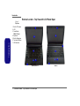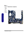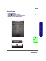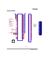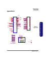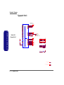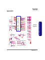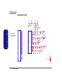
1
W210CUQ/ W211CU/ W215CU Preface Notebook Computer W210CUQ, W211CU, W215CU Service Manual Preface I Preface Notice The company reserves the right to revise this publication or to change its contents without notice. Information contained herein is for reference only and does not constitute a commitment on the part of the manufacturer or any subsequent vendor. They assume no responsibility or liability for any errors or inaccuracies that may appear in this publication nor are they in anyway responsible for any loss or damage resulting from the use (or misuse) of this publication. This publication and any accompanying software may not, in whole or in part, be reproduced, translated, transmitted or reduced to any machine readable form without prior consent from the vendor, manufacturer or creators of this publication, except for copies kept by the user for backup purposes. Preface Brand and product names mentioned in this publication may or may not be copyrights and/or registered trademarks of their respective companies. They are mentioned for identification purposes only and are not intended as an endorsement of that product or its manufacturer. Version 1.0 November 2011 Trademarks Intel and Intel Atom are trademarks of Intel Corporation. Windows® is a registered trademark of Microsoft Corporation. Other brand and product names are trademarks and /or registered trademarks of their respective companies. II Preface About this Manual This manual is intended for service personnel who have completed sufficient training to undertake the maintenance and inspection of personal computers. It is organized to allow you to look up basic information for servicing and/or upgrading components of the W210CUQ, W211CU, W215CU series notebook PC. The following information is included: Chapter 1, Introduction, provides general information about the location of system elements and their specifications. Chapter 2, Disassembly, provides step-by-step instructions for disassembling parts and subsystems and how to upgrade elements of the system. Preface Appendix A, Part Lists Appendix B, Schematic Diagrams Appendix C, Updating the FLASH ROM BIOS III Preface IMPORTANT SAFETY INSTRUCTIONS Follow basic safety precautions, including those listed below, to reduce the risk of fire, electric shock and injury to persons when using any electrical equipment: Preface 1. Do not use this product near water, for example near a bath tub, wash bowl, kitchen sink or laundry tub, in a wet basement or near a swimming pool. 2. Avoid using a telephone (other than a cordless type) during an electrical storm. There may be a remote risk of electrical shock from lightning. 3. Do not use the telephone to report a gas leak in the vicinity of the leak. 4. Use only the power cord and batteries indicated in this manual. Do not dispose of batteries in a fire. They may explode. Check with local codes for possible special disposal instructions. 5. This product is intended to be supplied by a Listed Power Unit with an AC Input of 100 - 240V, 50 - 60Hz, DC Output of 19V, 1.58A (30W) minimum AC/DC Adapter. IV Preface Instructions for Care and Operation The notebook computer is quite rugged, but it can be damaged. To prevent this, follow these suggestions: 1. Don’t drop it, or expose it to shock. If the computer falls, the case and the components could be damaged. Do not expose the computer to any shock or vibration. 2. Do not place anything heavy on the computer. Keep it dry, and don’t overheat it. Keep the computer and power supply away from any kind of heating element. This is an electrical appliance. If water or any other liquid gets into it, the computer could be badly damaged. Do not leave it in a place where foreign matter or moisture may affect the system. Don’t use or store the computer in a humid environment. Do not place the computer on any surface which will block the vents. Preface Do not expose it to excessive heat or direct sunlight. 3. Do not place it on an unstable surface. Follow the proper working procedures for the computer. Shut the computer down properly and don’t forget to save your work. Remember to periodically save your data as data may be lost if the battery is depleted. Do not turn off the power until you properly shut down all programs. Do not turn off any peripheral devices when the computer is on. Do not disassemble the computer by yourself. Perform routine maintenance on your computer. V Preface 4. 5. Avoid interference. Keep the computer away from high capacity transformers, electric motors, and other strong magnetic fields. These can hinder proper performance and damage your data. Take care when using peripheral devices. Use only approved brands of peripherals. Unplug the power cord before attaching peripheral devices. Preface Power Safety The computer has specific power requirements: VI • • Power Safety Warning • Before you undertake any upgrade procedures, make sure that you have turned off the power, and disconnected all peripherals and cables (including telephone lines). It is advisable to also remove your battery in order to prevent accidentally turning the machine on. • • • Only use a power adapter approved for use with this computer. Your AC adapter may be designed for international travel but it still requires a steady, uninterrupted power supply. If you are unsure of your local power specifications, consult your service representative or local power company. The power adapter may have either a 2-prong or a 3-prong grounded plug. The third prong is an important safety feature; do not defeat its purpose. If you do not have access to a compatible outlet, have a qualified electrician install one. When you want to unplug the power cord, be sure to disconnect it by the plug head, not by its wire. Make sure the socket and any extension cord(s) you use can support the total current load of all the connected devices. Before cleaning the computer, make sure it is disconnected from any external power supplies. Do not plug in the power cord if you are wet. Do not use the power cord if it is broken. Do not place heavy objects on the power cord. Preface Battery Precautions • Only use batteries designed for this computer. The wrong battery type may explode, leak or damage the computer. • Do not continue to use a battery that has been dropped, or that appears damaged (e.g. bent or twisted) in any way. Even if the computer continues to work with a damaged battery in place, it may cause circuit damage, which may possibly result in fire. • Recharge the batteries using the notebook’s system. Incorrect recharging may make the battery explode. • Do not try to repair a battery pack. Refer any battery pack repair or replacement to your service representative or qualified service personnel. • Keep children away from, and promptly dispose of a damaged battery. Always dispose of batteries carefully. Batteries may explode or leak if exposed to fire, or improperly handled or discarded. • Keep the battery away from metal appliances. • Affix tape to the battery contacts before disposing of the battery. • Do not touch the battery contacts with your hands or metal objects. Battery Guidelines Preface The following can also apply to any backup batteries you may have. • If you do not use the battery for an extended period, then remove the battery from the computer for storage. • Before removing the battery for storage charge it to 60% - 70%. • Check stored batteries at least every 3 months and charge them to 60% - 70%. Battery Disposal The product that you have purchased contains a rechargeable battery. The battery is recyclable. At the end of its useful life, under various state and local laws, it may be illegal to dispose of this battery into the municipal waste stream. Check with your local solid waste officials for details in your area for recycling options or proper disposal. Caution Danger of explosion if battery is incorrectly replaced. Replace only with the same or equivalent type recommended by the manufacturer. Discard used battery according to the manufacturer’s instructions. Battery Level Click the battery icon in the taskbar to see the current battery level and charge status. A battery that drops below a level of 10% will not allow the computer to boot up. Make sure that any battery that drops below 10% is recharged within one week. VII Preface Related Documents You may also need to consult the following manual for additional information: User’s Manual on DVD This describes the notebook PC’s features and the procedures for operating the computer and its ROM-based setup program. It also describes the installation and operation of the utility programs provided with the notebook PC. FCC Statement Preface This device complies with Part 15 of the FCC Rules. Operation is subject to the following two conditions: This device may not cause harmful interference. This device must accept any interference received, including interference that may cause undesired operation. VIII Preface System Startup Preface 1. Remove all packing materials. 2. Place the computer on a stable surface. 3. Insert the battery and make sure it is locked in position. 4. Attach the AC/DC adapter to the DC-In jack on the left of the computer, then plug the AC power cord into an outlet, and connect the AC power cord to the AC/DC adapter. 5. Use one hand to raise the lid/LCD to a comfortable viewing angle (do not exceed 120 degrees); use the other hand (as illustrated in <Hyperlink B n I>Figure 1) to support the base of the computer (Note: Never lift the computer by the lid/LCD). 6. Press the power button to turn the computer “on”. Figure 1 Opening the Lid/LCD/Computer with AC/DC Adapter Plugged-In IX Preface Preface X Preface Contents FCC Statement ........................................................................... 1-VIII System Startup ...............................................................................1-IX Introduction ..............................................1-1 Disassembly ...............................................2-1 Overview .........................................................................................2-1 Maintenance Tools ..........................................................................2-2 Connections .....................................................................................2-2 Maintenance Precautions .................................................................2-3 Disassembly Steps ...........................................................................2-4 Removing the Battery ......................................................................2-5 Removing the System Memory (RAM) ..........................................2-6 Removing the Wireless LAN Module .............................................2-8 Removing the Keyboard ..................................................................2-9 Removing the Hard Disk Drive .....................................................2-10 Part Lists ..................................................A-1 Parts List Illustration Location ....................................................... A-2 Top (W210CUQ) ............................................................................ A-3 Top (W211CU) .............................................................................. A-4 Top (W215CU) .............................................................................. A-5 Schematic Diagrams................................. B-1 System Block Diagram ...................................................................B-2 Cedarview CPU Part D ...................................................................B-3 Cedarview CPU Part A-C-F ...........................................................B-4 Cedarview CPU Part B ...................................................................B-5 Cedarview CPU Part E ...................................................................B-6 DDRIII SO-DIMM_0 .....................................................................B-7 IDT CLOCK ...................................................................................B-8 Tigerpoint Part A-B ........................................................................B-9 Tigerpoint Part C .........................................................................B-10 Tigerpoint Part D ..........................................................................B-11 Tigerpoint Part E-F .......................................................................B-12 Panel, HDD, LED .........................................................................B-13 BTB, 3G, WLAN, BT ...................................................................B-14 Audio Codec VT1812P .................................................................B-15 KBC-ITE IT8502E-J, TP, LID .....................................................B-16 TPM & HDMI ..............................................................................B-17 USB PORT & USB CHARGER ..................................................B-18 PWR AC IN, CHARGE ...............................................................B-19 PWR 1.5V, 0.75V .........................................................................B-20 PWR 1.05VS .................................................................................B-21 PWR SW, 1.8VS, 3VS, 5VS, 1.5VS ............................................B-22 PWR VCORE ...............................................................................B-23 PWR VDD3, 3.3V, VDD5V, SYS15V ........................................B-24 CRT ...............................................................................................B-25 Card Reader (w/ LAN) JMB261C ................................................B-26 BTB, USB, CCD, PWR SW .........................................................B-27 XI Preface Overview .........................................................................................1-1 Specifications ..................................................................................1-2 External Locator - Top View with LCD Panel Open ......................1-4 External Locator - Front & Right Side Views .................................1-5 External Locator - Left Side & Rear View .....................................1-6 External Locator - Bottom View .....................................................1-7 Mainboard Overview - Top (Key Parts) .........................................1-8 Mainboard Overview - Bottom (Key Parts) ....................................1-9 Mainboard Overview - Top (Connectors) .....................................1-10 Mainboard Overview - Bottom (Connectors) ...............................1-11 Bottom .......................................................................................... A-6 LCD (W210CUQ, W215CU) ........................................................ A-7 LCD (W211CU) ............................................................................ A-8 Preface Click Board .................................................................................. B-28 Power Button Board ..................................................................... B-29 Power Button for M1115 .............................................................. B-30 Updating the FLASH ROM BIOS......... C-1 Preface To update the FLASH ROM BIOS you must: C-1 Download the BIOS ....................................................................... C-1 Unzip the downloaded files to a bootable CD/DVD/ or USB Flash drive ................................................................................................ C-1 Set the computer to boot from the external drive ........................... C-1 Use the flash tools to update the BIOS .......................................... C-2 Restart the computer (booting from the HDD) .............................. C-2 XII Introduction Chapter 1: Introduction Overview This manual covers the information you need to service or upgrade the W210CUQ, W211CU, W215CU series notebook computer. Information about operating the computer (e.g. getting started, and the Setup utility) is in the User’s Manual. Information about dri-vers (e.g. VGA & audio) is also found in the User’s Manual. The manual is shipped with the computer. Operating system Window 7 has its own manuals as do application softwares (e.g. word processing and database programs). If you have questions about those programs, you should consult those manuals. 1.Introduction The W210CUQ, W211CU, W215CU series notebook is designed to be upgradeable. See Disassembly on page 2 - 1 for a detailed description of the upgrade procedures for each specific component. Please take note of the warning and safety information indicated by the “” symbol. The balance of this chapter reviews the computer’s technical specifications and features. Overview 1 - 1 Introduction Specifications Latest Specification Information 1.Introduction The specifications listed here are correct at the time of sending them to the press. Certain items (particularly processor types/speeds) may be changed, delayed or updated due to the manufacturer's release schedule. Check with your service center for more details. Processor Video Adapter (for N2600 Processor) Intel® Atom™ Processor N2600 1.60GHz, 32nm, 1MB L2 Cache, DDR3-800MHz, TDP: 3.5W Intel® GMA 3600 Video Integrated with the N2600 Processor Intel® Atom™ Processor N2800 1.86GHz, 32nm, 1MB L2 Cache, DDR3-1066MHz, TDP: 6.5W Display W210CUQ, W215CU: 10.1” (25.65cm) WSVGA TFT LCD (Thickness: 5.2mm) W211CU: 10.1” (25.65cm) WSVGA TFT LCD (Thickness: 3.6mm) Total Available Graphics Memory of up to 766MB MS DirectX® 9 compatible Storage One Changeable 2.5" 9.5mm (h) SATA Hard Disk Drive (Factory Option) External USB DVD Super Multi Drive Module Audio Core Logic High Definition Audio Compliant Interface 2 * Built-In Speakers Built-In Microphone Intel® NM10 Express Chipset Security CPU Memory Kensington Lock Slot BIOS Password TPM v1.2 The CPU is not a user serviceable part. Accessing the CPU in any way may violate your warranty. One 204 Pin SO-DIMM Socket Supporting DDR3 1066/ 1333MHz Memory (The real memory operating frequency depends on the FSB of the processor) Memory Expandable up to 2GB or 4GB* Depending on the Processor One 16Mb SPI Flash ROM Phoenix™ BIOS Three USB 2.0 Ports One Headphone-Out Jack One Microphone-In Jack One External Monitor Port One HDMI-Out Port One RJ-45 LAN Jack One DC-in Jack Video Adapter (for N2800 Processor) Keyboard Intel® GMA 3650 Video Integrated with the N2800 Processor “WinKey” keyboard (with embedded numeric keypad) *Atom™ N2600 Processors Only Support Up to 2GB of Memory BIOS Total Available Graphics Memory of up to 1790MB MS DirectX® 9 compatible 1 - 2 Specifications Interface Pointing Device Built-in Touchpad Introduction Card Reader Environmental Spec Embedded Multi-In-1 Card Reader MMC (MultiMedia Card) / RS MMC SD (Secure Digital) / Mini SD MS (Memory Stick) / MS Pro / MS Duo Temperature Operating: 5°C - 35°C Non-Operating: -20°C - 60°C Communication 10Mb/100Mb Ethernet LAN 300K Pixel USB PC Camera Module (Factory Option) 1.3M Pixel USB PC Camera Module (Factory Option) 3.75G/HSPA Mini-Card Module Dimensions & Weight W210CUQ: 266mm (w) x 185mm (d) x 19.7 - 27.1mm (h) 0.95kg (with 24.42WH Battery) W211CU: 266mm (w) x 185mm (d) x 18.5 - 25.4mm (h) 0.93kg (with 24.42WH Battery) 1.Introduction WLAN/ Bluetooth Half Mini-Card Modules: (Factory Option) Intel® Centrino® Wireless-N 100 Wireless LAN (802.11b/g/n) (Factory Option) Intel® Centrino® Wireless-N 1000 Wireless LAN (802.11b/g/n) (Factory Option) Intel® Centrino® Wireless-N 130 Wireless LAN (802.11b/g/n) + Bluetooth 3.0 (Factory Option) Third-Party Wireless LAN (802.11b/g/n) (Factory Option) Third-Party Wireless LAN (802.11b/g/n) + Bluetooth 3.0 Relative Humidity Operating: 20% - 80% Non-Operating: 10% - 90% W215CU 266mm (w) x 185mm (d) x 19.7 - 27.1mm (h) 0.96kg (with 24.42WH Battery) Power Full Range AC/DC Adapter AC Input: 100 - 240V, 50 - 60Hz DC Output: 19V, 1.58A (30W) Removable 3 Cell Smart Lithium-Ion Battery Pack, 24.42WH (Factory Option) Removable 6 Cell Smart Lithium-Ion Battery Pack, 48.84WH Specifications 1 - 3 Introduction Figure 1 External Locator - Top View with LCD Panel Open Top View 1. Built-In PC Camera 2. LCD 3. Power Button (Model C only) 4. Keyboard 5. Built-In Microphone 6. Touchpad & Buttons 7. LED Indicators 1 1 2 1.Introduction 2 3 4 6 4 6 5 5 7 7 W210CUQ, W211CU 1 - 4 External Locator - Top View with LCD Panel Open W215CU Introduction External Locator - Front & Right Side Views Figure 2 Front View 1. LED Indicators FRONT VIEW 1 Figure 3 Right Side View 1. Multi-in-1 Card Reader 2. 2 * USB 2.0 Ports 3. RJ-45 LAN Port 4. External Monitor Port 5. Power Button (Models A & B only) Right (W215CU) 1 2 2 3 4 Right ( W210CUQ, W211CU) 1 2 2 3 5 4 External Locator - Front & Right Side Views 1 - 5 1.Introduction RIGHT SIDE VIEW Introduction External Locator - Left Side & Rear View Figure 4 Left Side View Security Lock Slot DC-In Jack Vent HDMI-Out Port USB 2.0 Port Microphone-In Jack 7. Headphone-Out Jack / LEFT SIDE VIEW 1 2 3 4 1.Introduction 1. 2. 3. 4. 5. 6. Figure 5 Rear View 1. Battery REAR VIEW 1 1 - 6 External Locator - Left Side & Rear View 5 6 7 Introduction External Locator - Bottom View Figure 6 Bottom View 1. Battery 2. Component Bay Cover 3. Vent 4. Speakers 1 1.Introduction 3 2 4 4 Overheating To prevent your computer from overheating, make sure nothing blocks any vent while the computer is in use. External Locator - Bottom View 1 - 7 Introduction Figure 7 Mainboard Overview - Top (Key Parts) Mainboard Top Key Parts VT1802P ITE IT8518E JMC261C Multi-in-1 Card Reader Socket 1.Introduction 1. 2. 3. 4. 1 2 4 3 1 - 8 Mainboard Overview - Top (Key Parts) Introduction Mainboard Overview - Bottom (Key Parts) Figure 8 Mainboard Bottom Key Parts 1. CMOS Battery 2. Mini-Card Connector (WLAN Module) 3. Memory Slot DDR3 SO-DIMM 4. South Bridge 5. Embedded CPU 1.Introduction 5 4 1 2 3 Mainboard Overview - Bottom (Key Parts) 1 - 9 Introduction Figure 9 Mainboard Overview - Top (Connectors) 1.Introduction Mainboard Top Connectors 1. Keyboard Cable Connector 2. TouchPad Cable Connector 3. Speaker Cable Connector 4. Microphone Cable Connector 5. Switch Board Cable Connector 6. CCD Cable Connector 6 5 1 2 4 3 1 - 10 Mainboard Overview - Top (Connectors) Introduction Mainboard Overview - Bottom (Connectors) Figure 10 Mainboard Bottom Connectors 11 10 1 12 4 3 5 9 3 8 7 6 Mainboard Overview - Bottom (Connectors) 1 - 11 1.Introduction 2 1. External Monitor Port 2. RJ-45 Lan Port 3. USB Ports 4. LCD Cable Connector 5. CPU Fan Cable Connector 6. Headphone-Out Jack 7. Microphone-In Jack 8. USB Port 9. HDMI-Out Port 10. DC-In Jack 11. Batery Connector 12. HDD Connector 1.Introduction Introduction 1 - 12 Disassembly Chapter 2: Disassembly Overview This chapter provides step-by-step instructions for disassembling the W210CUQ, W211CU, W215CU series notebook’s parts and subsystems. When it comes to reassembly, reverse the procedures (unless otherwise indicated). We suggest you completely review any procedure before you take the computer apart. To make the disassembly process easier each section may have a box in the page margin. Information contained under the figure # will give a synopsis of the sequence of procedures involved in the disassembly procedure. A box with a lists the relevant parts you will have after the disassembly process is complete. Note: The parts listed will be for the disassembly procedure listed ONLY, and not any previous disassembly step(s) required. Refer to the part list for the previous disassembly procedure. The amount of screws you should be left with will be listed here also. Information A box with a will also provide any possible helpful information. A box with a contains warnings. An example of these types of boxes are shown in the sidebar. Warning Overview 2 - 1 2.Disassembly Procedures such as upgrading/replacing the RAM, optical device and hard disk are included in the User’s Manual but are repeated here for your convenience. Disassembly NOTE: All disassembly procedures assume that the system is turned OFF, and disconnected from any power supply (the battery is removed too). Maintenance Tools The following tools are recommended when working on the notebook PC: 2.Disassembly • • • • • • M3 Philips-head screwdriver M2.5 Philips-head screwdriver (magnetized) M2 Philips-head screwdriver Small flat-head screwdriver Pair of needle-nose pliers Anti-static wrist-strap Connections Connections within the computer are one of four types: 2 - 2 Overview Locking collar sockets for ribbon connectors To release these connectors, use a small flat-head screwdriver to gently pry the locking collar away from its base. When replacing the connection, make sure the connector is oriented in the same way. The pin1 side is usually not indicated. Pressure sockets for multi-wire connectors To release this connector type, grasp it at its head and gently rock it from side to side as you pull it out. Do not pull on the wires themselves. When replacing the connection, do not try to force it. The socket only fits one way. Pressure sockets for ribbon connectors To release these connectors, use a small pair of needle-nose pliers to gently lift the connector away from its socket. When replacing the connection, make sure the connector is oriented in the same way. The pin1 side is usually not indicated. Board-to-board or multi-pin sockets To separate the boards, gently rock them from side to side as you pull them apart. If the connection is very tight, use a small flat-head screwdriver - use just enough force to start. Disassembly Maintenance Precautions The following precautions are a reminder. To avoid personal injury or damage to the computer while performing a removal and/or replacement job, take the following precautions: •Before removing or servicing any part from the computer, turn the computer off and detach any power supplies. •When you want to unplug the power cord or any cable/wire, be sure to disconnect it by the plug head. Do not pull on the wire. 6. Peripherals – Turn off and detach any peripherals. 7. Beware of static discharge. ICs, such as the CPU and main support chips, are vulnerable to static electricity. Before handling any part in the computer, discharge any static electricity inside the computer. When handling a printed circuit board, do not use gloves or other materials which allow static electricity buildup. We suggest that you use an anti-static wrist strap instead. 8. Beware of corrosion. As you perform your job, avoid touching any connector leads. Even the cleanest hands produce oils which can attract corrosive elements. 9. Keep your work environment clean. Tobacco smoke, dust or other air-born particulate matter is often attracted to charged surfaces, reducing performance. 10. Keep track of the components. When removing or replacing any part, be careful not to leave small parts, such as screws, loose inside the computer. Power Safety Warning Before you undertake any upgrade procedures, make sure that you have turned off the power, and disconnected all peripherals and cables (including telephone lines). It is advisable to also remove your battery in order to prevent accidentally turning the machine on. Cleaning Do not apply cleaner directly to the computer, use a soft clean cloth. Do not use volatile (petroleum distillates) or abrasive cleaners on any part of the computer. Overview 2 - 3 2.Disassembly 1. Don't drop it. Perform your repairs and/or upgrades on a stable surface. If the computer falls, the case and other components could be damaged. 2. Don't overheat it. Note the proximity of any heating elements. Keep the computer out of direct sunlight. 3. Avoid interference. Note the proximity of any high capacity transformers, electric motors, and other strong magnetic fields. These can hinder proper performance and damage components and/or data. You should also monitor the position of magnetized tools (i.e. screwdrivers). 4. Keep it dry. This is an electrical appliance. If water or any other liquid gets into it, the computer could be badly damaged. 5. Be careful with power. Avoid accidental shocks, discharges or explosions. Disassembly Disassembly Steps The following table lists the disassembly steps, and on which page to find the related information. PLEASE PERFORM THE DISASSEMBLY STEPS IN THE ORDER INDICATED. To remove the Battery: 2.Disassembly 1. Remove the battery page 2 - 5 To remove the System Memory: 1. Remove the battery 2. Remove the system memory page 2 - 5 page 2 - 6 To remove the Wireless LAN Module: 1. Remove the battery 2. Remove the wireless LAN page 2 - 5 page 2 - 8 To remove the Keyboard: 1. Remove the battery 2. Remove the keyboard page 2 - 5 page 2 - 9 To remove the HDD: 1. Remove the battery 2. Remove the keyboard 3. Remove the HDD 2 - 4 Disassembly Steps page 2 - 5 page 2 - 9 page 2 - 10 Disassembly Removing the Battery 1. 2. 3. 4. Turn the computer off, and turn it over. Slide the latch 1 in the direction of the arrow (Figure 1a). Slide the latch 2 in the direction of the arrow, and hold it in place (Figure 1a). Slide the battery 63 in the direction of the arrow 4 (Figure 1b). a. 2 Figure 1 Battery Removal a. Slide the latch and hold in place. b. Slide the battery in the direction of the arrow. 1 2.Disassembly 3. Battery b. 3 4 Removing the Battery 2 - 5 Disassembly Figure 2 RAM Module Removal a. Remove the screw. b. Lift the bay cover up. Removing the System Memory (RAM) The computer has one memory socket for 200 pin Small Outline Dual In-line Memory Modules (SO-DIMM) supporting DDR3 1066/1333MHz Memory (real operation frequency of memory depends on FSB of processor). The main memory can be expanded up to 2GB. The SO-DIMM modules supported are 1024MB, and 2048MB and DDRIII Modules. The total memory size is automatically detected by the POST routine once you turn on your computer. Note: Atom™ N2600 Processors Only Support Up to 2GB of Memory Memory Upgrade Process 2.Disassembly Contact Warning Be careful not to touch the metal pins on the module’s connecting edge. Even the cleanest hands have oils which can attract particles, and degrade the module’s performance. 1. Turn off the computer, remove the battery (page 2 - 5). 2. Locate the component bay cover 1 , and remove screw 2 (Figure 2a). 3. Carefully lift the component bay cover 1 up (Figure 2b). a. b. 2 1 1. Component Bay Cover • 1 Screw 2 - 6 Removing the System Memory (RAM) 1 Disassembly 4. Gently pull the two release latches ( 3 & 4 ) on the sides of the memory socket in the direction indicated by the arrows (Figure 3c). Figure 3 RAM Module Removal (cont’d.) d. c. c. Pull the release latches. d. Remove the module. 3 4 5 2.Disassembly 5. The RAM module 5 will pop-up (Figure 3d), and you can then remove it. 6. Insert a new module holding it at about a 30° angle and fit the connectors firmly into the memory slot. 7. The module’s pin alignment will allow it to only fit one way. Make sure the module is seated as far into the slot as it will go. DO NOT FORCE the module; it should fit without much pressure. 8. Press the module in and down towards the mainboard until the slot levers click into place to secure the module. 9. Replace the bay cover and screw. 10. Restart the computer to allow the BIOS to register the new memory configuration as it starts up. 5. RAM Module Removing the System Memory (RAM) 2 - 7 Disassembly Figure 4 Wireless LAN Module Removal a. Remove the cover and disconnect the cables and remove the screw. b. The WLAN module will pop up. c. Lift the WLAN module out. Removing the Wireless LAN Module 1. 2. 3. 4. Turn off the computer, remove the battery (page 2 - 5) and the component bay cover (page 2 - 6). Carefully disconnect cables 1 & 2 , then remove screw 3 from the module socket (Figure 4a). The Wireless LAN module 4 (Figure 4b) will pop-up. Lift the Wireless LAN module 4 (Figure 4c) up and off the computer. a. c. 3 2.Disassembly 2 Note: Make sure you reconnect the antenna cable to ‘’1’’ + ‘’2’’socket (Figure b). 1 b. 4. WLAN Module. • 1 Screw 2 - 8 Removing the Wireless LAN Module 4 4 Disassembly Removing the Keyboard Figure 5 1. Turn off the computer and remove the battery (page 2 - 5). 2. Use only the small tool A provided (see picture below) to carefully press the four keyboard latches 1 - 4 at the top of the keyboard to elevate the keyboard from its normal position (Figure 5a). 3. Carefully lift the keyboard 5 up, being careful not to bend the keyboard ribbon cable 6 (Figure 5b). 4. Disconnect the keyboard ribbon cable 6 from the locking collar socket 7 (Figure 5b) 5. Carefully lift up the keyboard 5 (Figure 5c) off the computer. a. 1 2 3 4 Keyboard Removal a. Press the four latches to release the keyboard. b. Lift the keyboard up and disconnect the cable from the locking collar. c. Remove the keyboard. c. Tool for pressing the keyboard latches. Re-Inserting the Keyboard A 5 b. 7 6 When re-inserting the keyboard, align first the three keyboard tabs (Figure 5d) that are located at the bottom, to the slots in the case. d. 5 1. Keyboard Battery 5. 6. Keyboard Keyboard Tabs Removing the Keyboard 2 - 9 2.Disassembly Disassembly Figure 6 HDD Assembly Removal a. Locate the hard disk and remove the screw. Removing the Hard Disk Drive The hard disk drive can be taken out to accommodate other 2.5" serial (SATA) hard disk drives with a height of 9.5mm (h). Follow your operating system’s installation instructions, and install all necessary drivers and utilities (as outlined in Chapter 4 of the User’s Manual) when setting up a new hard disk. Hard Disk Upgrade Process 1. Turn off the computer, remove the battery (page 2 - 5) and remove the keyboard (page 2 - 9). 2. Locate the hard disk at point 1 and remove screw 2 (Figure 6a). 2.Disassembly a. 1 2 • 1 Screw HDD System Warning New HDD’s are blank. Before you begin make sure: You have backed up any data you want to keep from your old HDD. You have all the CD-ROMs and FDDs required to install your operating system and programs. If you have access to the internet, download the latest application and hardware driver updates for the operating system you plan to install. Copy these to a removable medium. 2 - 10 Removing the Hard Disk Drive Disassembly 3. 4. 5. 6. 7. Remove the HDD support module 63 (Figure 7b). Grip the mylar cover and slide the hard disk in the direction of arrow 4 (Figure 7b). Lift the hard disk 65 out of the bay 6 (Figure 7c). Remove the screws 7 & 8 and mylar cover 69 from the hard disk 65 (Figure 7d). Reverse the process to install a new hard disk (do not forget to replace all the screws and cover). Figure 7 HDD Assembly Removal (cont’d.) d. b. 8 9 2.Disassembly 4 b. Remove the HDD support module. Grip the mylar cover and slide the HDD in the direction of the arrow. c. Lift the HDD assembly out of the bay. d. Remove the screws and adhesive cover. 3 5 7 c. 6 5 3. HDD Support Module 5. HDD 9. Adhesive Mylar Cover • 2 Screws Removing the Hard Disk Drive 2 - 11 2.Disassembly Disassembly 2 - 12 Part Lists Appendix A:Part Lists This appendix breaks down the W210CUQ, W211CU, W215CU series notebook’s construction into a series of illustrations. The component part numbers are indicated in the tables opposite the drawings. Note: This section indicates the manufacturer’s part numbers. Your organization may use a different system, so be sure to cross-check any relevant documentation. Note: Some assemblies may have parts in common (especially screws). However, the part lists DO NOT indicate the total number of duplicated parts used. A.Part Lists Note: Be sure to check any update notices. The parts shown in these illustrations are appropriate for the system at the time of publication. Over the product life, some parts may be improved or re-configured, resulting in new part numbers. A - 1 Part Lists Parts List Illustration Location The following table indicates where to find the appropriate parts list illustration. Table A - 1 A.Part Lists Parts List Illustration Location A - 2 Parts List Illustration Location Parts W210CUQ, W211CU, W215CU Top (W210CUQ) page A - 3 Top (W211CU) page A - 4 Top (W215CU) page A - 5 Bottom page A - 6 LCD (W210CUQ, W215CU) page A - 7 LCD (W211CU) page A - 8 Part Lists Top (W210CUQ) Top (W210CUQ) A - 3 A.Part Lists Figure A - 1 Top (W210CUQ) Part Lists A.Part Lists Top (W211CU) Figure A - 1 Top (W211CU) Top A - 4 Top (W211CU) Part Lists Top (W215CU) Top (W215CU) A - 5 A.Part Lists Figure A - 1 Top (W215CU) Part Lists A.Part Lists Bottom Figure A - 2 Bottom A-6 Part Lists LCD (W210CUQ, W215CU) 非耐落 LCD (W210CUQ, W215CU) A - 7 A.Part Lists Figure A - 3 LCD (W210CUQ, W215CU) Part Lists A.Part Lists LCD (W211CU) Figure A - 4 LCD (W211CU) A - 8 LCD (W211CU) Part Lists A.Part Lists LCD (W211CU) A - 9 A.Part Lists Part Lists A - 10 LCD (W211CU) Schematic Diagrams Appendix B: Schematic Diagrams Table B - 1 This appendix has circuit diagrams of the W210CUQ, W211CU, W215CU notebook’s PCB’s. The following table indicates where to find the appropriate schematic diagram. Diagram - Page Diagram - Page System Block Diagram - Page B - 2 Tigerpoint Part E-F - Page B - 12 PWR SW, 1.8VS, 3VS, 5VS, 1.5VS - Page B - 22 Cedarview CPU Part D - Page B - 3 Panel, HDD, LED - Page B - 13 PWR VCORE - Page B - 23 Cedarview CPU Part A-C-F - Page B - 4 BTB, 3G, WLAN, BT - Page B - 14 PWR VDD3, 3.3V, VDD5V, SYS15V - Page B - 24 Cedarview CPU Part B - Page B - 5 Audio Codec VT1812P - Page B - 15 CRT - Page B - 25 Cedarview CPU Part E - Page B - 6 KBC-ITE IT8502E-J, TP, LID - Page B - 16 Card Reader (w/ LAN) JMB261C - Page B - 26 DDRIII SO-DIMM_0 - Page B - 7 TPM & HDMI - Page B - 17 BTB, USB, CCD, PWR SW - Page B - 27 IDT CLOCK - Page B - 8 USB PORT & USB CHARGER - Page B - 18 Click Board - Page B - 28 Tigerpoint Part A-B - Page B - 9 PWR AC IN, CHARGE - Page B - 19 Power Button Board - Page B - 29 Tigerpoint Part C - Page B - 10 PWR 1.5V, 0.75V - Page B - 20 Power Button for M1115 - Page B - 30 Tigerpoint Part D - Page B - 11 PWR 1.05VS - Page B - 21 Version Note The schematic diagrams in this chapter are based upon version 6-7PW2105-001. If your mainboard (or other boards) are a later version, please check with the Service Center for updated diagrams (if required). B - 1 B.Schematic Diagrams Diagram - Page SCHEMATIC DIAGRAMS Schematic Diagrams System Block Diagram 6-7P -W2105- 001 DDR 3 On e C han nel 1GB & 2 GB Mem ory Ter min ati on IO : 6- 7 1- W2 1 01 - D0 1 PW R SW: 6 -7 1 -M1 1 5S -D 0 2( M11 1 5) DDR3 Use EDP LCD NB 1366x7 68 ELD 1920x 1080 B.Schematic Diagrams PW R SW: 6 -7 1 -M1 1 0S -D 0 3( M11 0 0M) C LICK : 6 -7 1- M1 10 2 -D 0 1A <7.5" 1 280 x800 LCD CONNECTOR <8" CL IC K B OA RD TOUCH PAD CRT OUT SO-DIMM0 Intel Cedarview 32nm TDP 3.5W 1 920 x120 0 D ire ct X 10. 1 3.3V,5V,3VS,5VS,1.8VS 14 .31 8 MHz Colck Generator IDT 9VRS4338 17.1mm*8.1mm*1.2mm TSSOP 64PIN 1.05VS,1.5VS 1.5V,0.75VS(VTT_MEM) AC-IN,CHARGER 1 .65 Gb/s HDMI CONNECTOR Sheet 1 of 29 System Block Diagram VDD3,VDD5 CLEVO Ce da r Rock -Ne tX Sys te m Bloc k Diagra m MB :6 - 71 -W 2 10 0 -D 0 1 VCORE+ GFX C 0/C 1/C 2/C 3/C4 800 /106 7MT /s PROCESSOR F CBGA 559 pin MI C IN 2 2mm *22 mm* 2.35 mm HP OU T IN T SPK R NB 2X E LD 4X 32 .7 68 KH z EC ITE 8518 X4/X 2-G EN1 10 G bit s/s DMI Azalia Codec VT1802 <=8" 0.1"~13 SOUTH BRIDGE INT. K/B LPC 3 3 M Hz 0.5"~11" EC SMBUS THERMAL SENSOR G711ST9U SMART FAN 24 MHz PCIE 100 MHz <12" Tiger Point 3 60 MM AP SMART BATTERY 1 7mm *17 mm* 1.06 mm 3 2. 768 KH z Mini Card WLAN Bluetooth(USB5) SATA I/II 3.0Gb/s <12" USB2.0 4 80 Mbp s S HEE T 12 B - 2 System Block Diagram IN T MIC AZALIA LINK S HEE T 15 SATA HDD 9*9 *1.6mm SYSTEM SMBUS 14*14*1.6mm HSPI ROM IN T SPK L 48 pin s QFN 1 28p in s L QF P (USB2) Port_2 Mini PCIE 3G CARD (USB4) (USB7) CCD JMC261C LAN CARD READER 25 MHz 1"~16" (USB0) Port_0 (USB1) Port_1 RJ-45 Card Reader Socket Schematic Diagrams Cedarview CPU Part D U 12 D 1. 8V S C EDARVIEW 1. 8V S R E V = 1. 10 R 29 R3 7 *2 20_ 04 * 220 _04 1. 05 VS L 26 H _R S VD _ K2 8 H _R S V D_ L2 7 L 27 H _R S V D_ K2 8 K 28 K 25 J 28 H _R S V D_ L2 7 K 26 R 28 R3 4 2 .2 K_ 04 K 27 H 27 2 . 2K _04 R SV D _L 26 S MI # ST R AP _L 27 N MI / LI N T1 0 ST R AP _K 28 R SV D _K 25 R SV D _J 28 R SV D _K 26 R SV D _C 1 8 S TP C LK # ICH H _ SMI # 9 H _ N MI 9 H _N MI H _A 20 M# R9 R8 R1 4 *1K _0 4 *1K _0 4 1K _0 4 *1K _0 4 H _S TP C LK # H _ A2 0M# 9 H _ ST PC L K# 9 H _S TP C LK # R1 2 H _ D PR S TP # 10 H _ D PS LP # 10 H _ C PU S LP # 9 H _C P U SL P # R1 96 H _I N I T# R7 *1K _0 4 H _I N TR R1 3 *1K _0 4 R SV D _H 2 7 R SV D _K 30 R SV D _L 29 R SV D _L 30 D P R S TP # C2 1 B 21 J 31 R SV D _K 29 R SV D _J 31 D P LS LP # C P U S LP # B 22 H _C P U S LP # A 23 H _I N I T# I IT # N I N TR / LI N T0 0 D2 0 H _I N T R H V_ G PI O _R C O MP TH E R MTR I P # B 20 L 11 MV_ G PI O _R C O MP R S V D_ L1 1 H _ I NI T # H _ I NT R 9 9 H _ TH E R MTR I P# 9 P R O C H O T # m u s t b e te rm i n a te d w i th a 5 6 -O , p u l l -u p re s i s to r to V C C P e v e n fi i t i s n o t us e d . C2 0 PB E # H _ FE R R # 9 A 19 D2 3 P RO C H O T # P WR G O O D R E S ET # DB R# H _P R O C H O T# H _ PR O C H O T# 2 2 G3 0 H _ PW R G D 1 0 E 30 P LT R ST # 10 H _P R O C H O T# R1 95 10 0_0 4 1. 8V S P RDY # P R E Q# 1. 05 VS *1K _0 4 H2 9 H _R S V D _H 29 H _R S V D_ H 29 R3 0 *51 _0 4 G2 9 H _R S V D _G 29 H _R S V D_ G 29 R2 5 51 _04 Sheet 2 of 29 Cedarview CPU Part D J 19 R1 1 R 1 86 51_ 04 51_ 04 H _T D I H _T D O R1 0 51_ 04 H _T MS H P LL_ R EF C LK _P C LK _C P U _H P L 7 K 19 H P LL_ R EF C LK CPU C LK _C P U _H P L# 7 E 19 F 19 R S VD _ E1 9 R S VD _ F1 9 CAD N ote: H_CP U_SVI DALR T#_R, H_CPU _SVI DDAT_ R Place the PU r esist ors close to C PU 1. 05 VS EM I C 22 6 H_ TC K C 25 H_ TD I C 24 H_ TD O H_ TMS H_ TR S T# B 25 D 24 B 24 *0 .1 u_ 16V _Y 5 V_ 04 R5 R6 W 25 W 26 N 24 N 25 R5 51_ 04 H _T C K R6 51_ 04 H _T R ST # TC LK TD I S VI D _ AL ER T # SV I D _C LK TD O B 16 H _C P U _S V ID A LR T #_ R D1 8 H _C P U _S V ID C L K_ R R 19 0 R 18 7 *10 mi l_s ho rt *10 mi l_s ho rt C1 6 H _C P U _S V ID D A T_ R R 18 9 *10 mi l_s ho rt H _C P U_ S VI D A LR T# 2 2 H _C P U_ S VI D C LK 22 H _C P U_ S VI D D A T 22 S VI D _D A TA TMS TR S T# C AD No te: H_CPU _SVID CLK_ R P lace the PU r esist ors close to V R R SV D _R 5 R SV D _R 6 R SV D _W 25 R SV D _W 26 R S VD _ K2 1 R SV D _N 2 4 R SV D _N 2 5 R S V D_ L2 2 R S V D_ L2 4 K 21 L 22 L 24 SVID Signals 1. 0 5V S 4 OF 6 H _C P U _S VI D A LR T #_R R 198 H _C P U _S VI D C LK _ R R 188 H _C P U _S VI D D A T_ R R 197 C D V _22 MM_R E V1 P1 0_5 L A Y OU T N OT E : 75 _1 %_0 4 54 . 9_1 %_0 4 11 0_ 1%_ 04 P l ac e t e rm i n a tio n n e a r C P U T he rm al IC 3 . 3V 1 D 03 2 P TH 3 3. 3V 10 K_ N TC _0 6 Q1 6 2 1 VC C OU T 1:2 (4mils:8mils) C2 52 3 G ND *0. 1u _10 V_ X7 R _04 *G 71 1S T9U C 25 1 TH E R M_ V OL T 15 8/30 R 2 01 *0. 1 u_1 0V _X 7R _0 4 1 0K _1% _04 1 5, 15 , 21 1. 8 VS 8, 1 0, 11 ,1 2, 13 , 15, 1 7, 19 ,2 0, 21 , 22 3. 3 V 3 , 6, 7, 8, 9 1 , 0, 11 , 12, 1 3, 14 ,1 5, 16 , 21 3. 3 VS 5 ,7 , 9, 10 ,1 1, 20 , 22 1. 0 5V S 3 PLACE NEAR CPU 2 Cedarview CPU Part D B - 3 B.Schematic Diagrams 49 .9 _1 %_0 4 H _S MI # L 30 K 29 H V _G P I O _R C O MP K 24 MV _G P I O _R C O MP K 23 4 9. 9_ 1%_ 04 H _N MI H _A 20 M# R SV D _K 27 R SV D _H 3 0 R 36 H _S MI # C2 2 C1 8 D2 2 K 30 L 29 H 30 R3 5 B 18 Schematic Diagrams Cedarview CPU Part A-C-F DM I Sign al Gr ou p U1 2 A Z d iff = 80 Oh m ? 7.5% C E D A R V IE W l en gt h =b r eak ou t( <=50 0mils) +(< = 6000 mils) 8 8 8 8 8 8 8 8 D D D D D D D D MI _ I C MI _ I C MI _ I C MI _ I C MI _ I C MI _ I C MI _ I C MI _ I C H_ H_ H_ H_ H_ H_ H_ H_ IT _ IT _ IT _ IT _ IT _ IT _ IT _ IT _ MR MR MR MR MR MR MR MR 7 7 C L K _C P U _ D M I C L K _C P U _ D M I # 0 0 1 1 2 2 3 3 _D _D _D _D _D _D _D _D C2 3 7 C2 3 6 C2 4 0 C2 3 8 C2 4 3 C2 4 2 C2 4 8 C2 4 9 3 /7 P N P N P N P N 0 . 1 u_ 0 . 1 u_ 0 . 1 u_ 0 . 1 u_ *0 . 1 u *0 . 1 u *0 . 1 u *0 . 1 u 1 0 V _ X 7R _ 0 4 1 0 V _ X 7R _ 0 4 1 0 V _ X 7R _ 0 4 1 0 V _ X 7R _ 0 4 _ 10 V _ X 7 R _ 0 4 _ 10 V _ X 7 R _ 0 4 _ 10 V _ X 7 R _ 0 4 _ 10 V _ X 7 R _ 0 4 D D D D D D D D MI _ MI _ MI _ MI _ MI _ MI _ MI _ MI _ R R R R R R R R XP XN XP XN XP XN XP XN _0 _0 _1 _1 _2 _2 _3 _3 L3 L2 M 3 M 2 N 2 N 1 P2 P3 N 9 N 8 T2 D D D D D D D D MI _ MI _ MI _ MI _ MI _ MI _ MI _ MI _ R R R R R R R R XP XN XP XN XP XN XP XN R E V = 1 .1 0 0 0 1 1 2 2 3 3 D M I _ TX P 0 D MI _ T X N 0 D M I _ TX P 1 D MI _ T X N 1 D M I _ TX P 2 D MI _ T X N 2 D M I _ TX P 3 D MI _ T X N 3 DMI D MI _ R E F C L K P D MI _ R E F C L K N D MI _ R E F 1 P 5 RS V D_ T P _ R8 RS V D_ T P _ R7 D M I _ R C OM P K6 K5 L5 L6 L9 L8 N5 N6 DM DM DM DM DM DM DM DM R8 R7 T1 D M I _R C O M P I _T X P _ 0 I _T X N _0 I _T X P _ 1 I _T X N _1 I _T X P _ 2 I _T X N _2 I _T X P _ 3 I _T X N _3 R 41 R 40 R 39 R 38 D D D D D D D D *0 _ 0 4 *0 _ 0 4 *0 _ 0 4 *0 _ 0 4 MI MI MI MI MI MI MI MI _I C _I C _I C _I C _I C _I C _I C _I C H_ H_ H_ H_ H_ H_ H_ H_ M M M M M M M M T _I T _I T _I T _I T _I T _I T _I T _I R0 R0 R1 R1 R2 R2 R3 R3 _ _ _ _ _ _ _ _ DP DN DP DN DP DN DP DN 8 8 8 8 8 8 8 8 DM I_RCOM P len gt h < 500mils 1 OF 6 C D V _ 2 2 MM _R E V 1 P 1 0 _ 5 1 . 5 V S _ DM I RE F L47 1 .5 V S *H C B 1 0 0 5K F -1 2 1T 2 0 _ sh o r t R2 0 9 7 . 5 K _ 1 %_ 0 4 (1) CRT DAC Sign al Gr ou p CRT _RED,CRT_GREEN, CRT _BL UE VGA RGBr e sis to r s co ls e t o M CHb all Zo = 37.5 Ohm ? 5% sig na l : 9 mils len gt h < 800 mils Tw o VGA RGBr e sis to rs b et we en Zo = 50 Oh m ? 5% sig na l : 5 mils len gt h < 14000 mils C 256 1 u _ 6 . 3V _X 5 R _0 4 B.Schematic Diagrams 3 . 3V S (2) CRT Syn c Sign al Gr ou p DAC_HSYNC,DAC_VSYNC Zo = 50 Oh m ? 5 % sig na l : 5 mils len gt h < 14500 mils (3) CRT Co n tr ol Sig nal Gr o up CRT_ DDC_CLK,CRT _DDC_DAT A Zo = 50 Oh m ? 5% sig nal : 5 mils len gt h < 15100 mil s U1 2 C D03 R 18 R 19 1 0 K_ 0 4 1 0 K _ 04 C E D A R V IE W RE V H 25 J22 1 6 H D M I _C T R L C LK 1 6 H D MI _ C T R L D A TA C 8 B8 16 Sheet 3 of 29 Cedarview CPU Part A-C-F 1 1 1 1 1 1 16 16 6 6 6 6 6 6 P O R TC _ H P C P OR T C _ H P C H H H H H H H H H D MI C _ C 0 C P H DM IC_ C 0 CN H D MI C _ C 1 C P H DM IC_ C 1 CN H D MI C _ C 2 C P H DM IC_ C 2 CN H D MI C _ C L K C P H D M I C _ C LK C N DM DM DM DM DM DM DM DM IC IC IC IC IC IC IC IC _C _C _C _C _C _C _C _C 0 0 1 1 2 2 L L H 22 CP CN CP CN CP CN K CP K CN G 2 G 3 F3 F2 D 4 C 3 B7 A7 H 15 J15 1. 5 V S DD I_ DD C_ S D A D0 3 D DI 1 D I S A B L E : 2. 2 K T O G N D R1 5 *H C B 1 0 0 5K F -1 21 T 2 0 _s h o r t F25 G 27 R 20 D 10 C 10 2 .2 K_ 0 4 D 26 R2 1 7. 5 K _ 1 % _ 04 C2 0 1 U _ 6 . 3 V _ X 5R _ 0 4 B R E F _ 1P 5V B RE F _ RE X T A Z _ B IT C L K A Z _ S Y NC 10 1 0 ,1 4 AZ _ SD IN 1 A Z _ S D OU T 10 , 1 4 AZ_ R ST# DD I0 _ DD C_ S C L DD I0 _ DD C_ S D A C RT _ RE D C R T_ G R E E N C R T _B LU E DD I0 _ A UX P DD I0 _ A UX N DD I0 _ HP D DD DD DD DD DD DD DD DD I0 I0 I0 I0 I0 I0 I0 I0 _ _ _ _ _ _ _ _ DD I C R T_ I R T N C R T_ I R E F VG A T XP 0 T XN 0 T XP 1 T XN 1 T XP 2 T XN 2 T XP 3 T XN 3 C R T _ D D C _D A T A C R T_ D D C _ C L K D P L _ RE F S S CC L K P D P L _R E F S S C C LK N D P L _ RE F C L K P D P L_ R E F C LK N RS V D_ T P _ H1 5 RS V D_ T P _ J 1 5 L VDS _ C T RL _ CL K LV D S _ C TR L _D A T A DD I1 _ DD C_ S C L DD I1 _ DD C_ S D A L V DS _ D DC _ CL K LV D S _ D D C _D A T A DD I1 _ A UX P DD I1 _ A UX N L V D S _I B G L V DS_ V B G DD I1 _ HP D E1 F1 J1 H 1 F1 E1 J1 K1 10 , 1 4 1 0 ,1 4 C RT _ HS Y N C C R T_ V S Y N C = 1. 1 0 1 1 1 1 3 3 3 3 J17 H 17 E1 5 F15 H 21 F22 R 49 R 44 9 0 . 9_ 1 % _ 0 4 H _ A Z I L_ B C L K 9 0 . 9_ 1 % _ 0 4 H _ A Z I L_ S Y N C R 45 R 48 H _ A Z I L_ S D I 3 3 _0 4 9 0 . 9_ 1 % _ 0 4 H _ A Z I L_ S D O E2 2 F21 R 47 9 0 . 9_ 1 % _ 0 4 H _ A Z I L_ R S T # E2 1 D0 3 DD DD DD DD DD DD DD DD I1 I1 I1 I1 I1 I1 I1 I1 _ _ _ _ _ _ _ _ T XP 0 T XN 0 T XP 1 T XN 1 T XP 2 T XN 2 T XP 3 T XN 3 L V D S _ VRE F H L V D S _V R E F L L VDS L V D S _ TX P 0 L V DS _ T X N0 L V D S _ TX P 1 L V DS _ T X N1 L V D S _ TX P 2 L V DS _ T X N2 L V D S _ TX P 3 L V DS _ T X N3 RS V D_ T P _ J 1 7 RS V D_ T P _ H1 7 BR EF 1 P5 V B R E F R E XT A Z I L _ B C LK A Z IL _ S Y NC L V D S _C L K P LV D S _ C LK N IHDA P A N E L _ B K L T C TL P A N E L _ B K L TE N P A N E L_ V D D E N A Z IL _ S D I A Z IL _ S D O A Z I L _ R S T# C D V _ 2 2M M_ R E V 1 P 1 0 _ 5 3 OF D A C_ R E D D A C_ G RE E N D A C_ B L U E D1 4 C1 4 D A C_ H S Y N C D A C_ V S Y N C B 12 B 11 C1 1 DA C _ RE D D A C _ GR E E N DA C _ B L UE D1 2 A 13 DA C RE F S E T (2) D A C _ R E D 13 D A C_ G RE E N 1 3 D A C_ B L U E 1 3 (1) D A C _ D D C A D A TA 13 D A C_ D DC A CL K 13 F 17 E 17 D P L _R E F C L K P D P L _R E F C L K N F 28 E 24 L C T L A _ C LK L CT L B _ D A T A 1 50 _ 1 % _ 04 1 50 _ 1 % _ 04 1 50 _ 1 % _ 04 Pla ce VGA RGBr es is to rs clo se to M CH < 800 mils t o M CH ball D A CR E F S E T R1 9 9 6 19 _ 1 % _ 04 Pla ce DACREF SET r es ist or clo se t o M CH (3) < 500 mils t o M CH ball O P T ION C L K _D R E F S S 7 C L K _D R E F S S # 7 B9 A9 R1 9 1 R1 9 3 R1 9 2 LAYOUT NOT E: LAYOUT NOT E: E 29 E 27 3 .3 V S R 4 1 M _0 4 G2 4 H2 4 L _ D D C _ C LK L _D D C _ D A TA E 10 F 10 L V D _I B G T P_ L V D_ V B G H2 H3 L V D _V R E F H _ O U T _R L V D _V R E F L _ O U T _ R L VD S _ B K L T CT L R2 6 R1 6 R1 7 L V D _I B G R2 4 L V D _V R E F H _ O U T _R L V D _V R E F L _ O U T _ R R2 3 R2 2 2 . 2 K _0 4 2 . 2 K _0 4 X5 1 2 P N P N P N 12 12 12 12 12 12 L V D S -L C L K P L V D S - LC L K N 12 12 C 14 C 13 2 2 p _ 50 V _ N P O _ 0 4 2 2 p _ 50 V _ N P O _ 0 4 2 . 3 7K _ 1 % _ 0 4 *1 0 m li _ s ho rt *1 0 m li _ s ho rt (1) * 10 K _ 0 4 MC H _ B L O N 1 2 LV D D _E N 1 2 5 , 7 , 8, 11 , 2 1 6 , 7, 8, 9 , 1 0 , 1 1 , 1 2, 1 3 , 1 4 , 1 5, 16 , 2 1 6 ( 1) L VDS Clock & Da ta Sign al Gr o up L C T L A _ C LK L CT L B _ D A T A F S X 8 L_ 2 7 MH z L V D S - L0 L V D S -L 0 L V D S - L1 L V D S -L 1 L V D S - L2 L V D S -L 2 H4 J4 G2 2 E 25 F 29 12 12 T1 G1 0 H1 0 F8 E8 H7 H8 G5 G6 Z dif f = 9 0 Ohm ? 0% s ign al / s pac e : 4 / 5 mils le ng th < 785 0 mils B - 4 Cedarview CPU Part A-C-F 13 13 (2 ) LVDS Co nt r ol Sig nal Gr o up LBKLT _CTL ,LBKL T_ EN,L VDD_EN Zo = 50 Ohm ? 0% si gn al : 5 mils le ng th < 6000 mils 1 .5 V S 3 .3 V S Schematic Diagrams Cedarview CPU Part B 6 M_A_A0 M_A_A1 M_A_A2 M_A_A3 M_A_A4 M_A_A5 M_A_A6 M_A_A7 M_A_A8 M_A_A9 M_A_A10 M_A_A11 M_A_A12 M_A_A13 M_A_A14 M_A_A15 1.5 V LA YO UT NO TE: R203 6 6 6 Pl ac e r e s is t or s a nd C AP c los e t o DDR _V REF pin 6 6 6 1K_1%_04 MCH_ VREF C253 1K_1%_04 0.1u _16V_Y5 V_0 4 Width 8mil Spacing 8 mil < 3 00mil M_A_WE# M_A_CAS# M_A_RAS# M_A_BS0 M_A_BS1 M_A_BS2 6 6 M_ CS2 # M_ CS3 # 6 6 M_ CKE2 M_ CKE3 6 6 M_ ODT2 M_ ODT3 LA YO UT NO TE: 6 M_CL K_D DR2 6 M_CL K_D DR2# 6 M_CL K_D DR3 6 M_CL K_D DR3# Width 4mil Spacing 5 mil AK1 4 AK1 6 AJ1 4 AJ1 6 AK1 8 AH1 8 AJ1 8 AK2 0 AJ2 0 AH2 0 AJ1 2 AK2 1 AJ2 1 AJ 8 AH2 2 AJ2 2 AH1 0 AJ1 0 AJ1 1 AK1 2 AH1 3 AK2 2 AH1 2 AH 8 AK1 1 AK8 AH2 3 AJ2 4 AK2 4 AH2 4 AK1 0 AK7 AL 9 AJ 7 AG1 5 AF1 5 AF1 7 AG1 7 AD1 7 AC1 7 AC1 5 AD1 5 AK2 5 6 DDR3_D RAMR ST# R208 MC H_VREF AJ2 7 AL2 8 100K_04 7 CLK_DDR 3REF_ CLK 7 CLK_DDR3 REF_CL K# 10, 15 DELAY _ALL_SYS_PWRGD R19 4 10 DDR3 _DRAM_PWROK 12K_1%_04 R2 00 10 K_ 1%_ 04 R206 R207 R205 274_1 %_0 4 22.6 _1%_04 33.2 _1%_04 AC1 9 AB1 9 AA5 W7 DDR 3_ODTPU AJ2 6 DDR 3_CMDPU AJ2 5 DDR 3_DQPU AK2 7 CPU_R SVD_TP_0 3 AB1 1 CPU_R SVD_TP_0 4 AB1 3 AF1 9 AG1 9 T2 T3 6 6 6 6 6 6 6 6 M_A_DM0 M_A_DM1 M_A_DM2 M_A_DM3 M_A_DM4 M_A_DM5 M_A_DM6 M_A_DM7 Y2 8 AB2 6 AE3 0 AB2 1 AG1 1 AG 2 AB8 AA3 DDR 3_MA0 DDR 3_MA1 DDR 3_MA2 DDR 3_MA3 DDR 3_MA4 DDR 3_MA5 DDR 3_MA6 DDR 3_MA7 DDR 3_MA8 DDR 3_MA9 DDR 3_MA10 DDR 3_MA11 DDR 3_MA12 DDR 3_MA13 DDR 3_MA14 DDR 3_MA15 CED ARVIEW REV = 1. 10 DDR 3_WE# DDR 3_CAS# DDR 3_RAS# DDR 3_BS0 DDR 3_BS1 DDR 3_BS2 DDR 3_CS#0 DDR 3_CS#1 DDR 3_CS#2 DDR 3_CS#3 DDR 3_CKE0 DDR 3_CKE1 DDR 3_CKE2 DDR 3_CKE3 DDR 3_ODT0 DDR 3_ODT1 DDR 3_ODT2 DDR 3_ODT3 D DR3 DDR 3_CK0 DDR 3_CK#0 DDR 3_CK1 DDR 3_CK#1 DDR 3_CK2 DDR 3_CK#2 DDR 3_CK3 DDR 3_CK#3 DDR 3_DRAMRST# DDR 3_VREF DDR 3_VREF_N CTF DDR 3_REFP DDR 3_REFN DDR 3_DRAM_PWROK DDR 3_VCCA_PWROK DDR 3_ODTPU DDR 3_CMDPU DDR 3_DQPU DD R3_DQ0 DD R3_DQ1 DD R3_DQ2 DD R3_DQ3 DD R3_DQ4 DD R3_DQ5 DD R3_DQ6 DD R3_DQ7 DD R3_DQ8 DD R3_DQ9 DDR3 _DQ10 DDR3 _DQ11 DDR3 _DQ12 DDR3 _DQ13 DDR3 _DQ14 DDR3 _DQ15 DDR3 _DQ16 DDR3 _DQ17 DDR3 _DQ18 DDR3 _DQ19 DDR3 _DQ20 DDR3 _DQ21 DDR3 _DQ22 DDR3 _DQ23 DDR3 _DQ24 DDR3 _DQ25 DDR3 _DQ26 DDR3 _DQ27 DDR3 _DQ28 DDR3 _DQ29 DDR3 _DQ30 DDR3 _DQ31 DDR3 _DQ32 DDR3 _DQ33 DDR3 _DQ34 DDR3 _DQ35 DDR3 _DQ36 DDR3 _DQ37 DDR3 _DQ38 DDR3 _DQ39 DDR3 _DQ40 DDR3 _DQ41 DDR3 _DQ42 DDR3 _DQ43 DDR3 _DQ44 DDR3 _DQ45 DDR3 _DQ46 DDR3 _DQ47 DDR3 _DQ48 DDR3 _DQ49 DDR3 _DQ50 DDR3 _DQ51 DDR3 _DQ52 DDR3 _DQ53 DDR3 _DQ54 DDR3 _DQ55 DDR3 _DQ56 DDR3 _DQ57 DDR3 _DQ58 DDR3 _DQ59 DDR3 _DQ60 DDR3 _DQ61 DDR3 _DQ62 DDR3 _DQ63 DDR3_ DQS0 DDR3_ DQS1 DDR3_ DQS2 DDR3_ DQS3 DDR3_ DQS4 DDR3_ DQS5 DDR3_ DQS6 DDR3_ DQS7 RSVD_TP_AB1 1 RSVD_TP_AB1 3 RSVD_TP_AF1 9 RSVD_TP_AG19 DDR 3_DM0 DDR 3_DM1 DDR 3_DM2 DDR 3_DM3 DDR 3_DM4 DDR 3_DM5 DDR 3_DM6 DDR 3_DM7 D DR3_DQ S#0 D DR3_DQ S#1 D DR3_DQ S#2 D DR3_DQ S#3 D DR3_DQ S#4 D DR3_DQ S#5 D DR3_DQ S#6 D DR3_DQ S#7 Y30 Y29 AC30 AC31 W31 W28 AB2 8 AB3 0 AA2 4 AA2 2 AE2 7 AE2 6 AB2 7 AA2 5 AD25 AD27 AD29 AE2 9 AJ30 AK2 9 AD28 AD30 AG30 AJ29 AE2 4 AG24 AD22 AC21 AG27 AG25 AG21 AE2 1 AD13 AD11 AG8 AG7 AG13 AE1 3 AD10 AF8 AH2 AG3 AD2 AD3 AH4 AK3 AE2 AD4 AD7 AD6 AA6 AB5 AE8 AE5 AB9 AA8 AB2 AB4 W4 V3 AC2 AB3 Y2 W1 AA3 0 AB2 4 AF3 0 AE2 2 AG10 AF4 AB6 Y3 AA3 1 AB2 5 AF2 9 AF2 2 AF1 0 AF3 AB7 AA2 M_A_DQ0 M_A_DQ1 M_A_DQ2 M_A_DQ3 M_A_DQ4 M_A_DQ5 M_A_DQ6 M_A_DQ7 M_A_DQ8 M_A_DQ9 M_A_DQ10 M_A_DQ11 M_A_DQ12 M_A_DQ13 M_A_DQ14 M_A_DQ15 M_A_DQ16 M_A_DQ17 M_A_DQ18 M_A_DQ19 M_A_DQ20 M_A_DQ21 M_A_DQ22 M_A_DQ23 M_A_DQ24 M_A_DQ25 M_A_DQ26 M_A_DQ27 M_A_DQ28 M_A_DQ29 M_A_DQ30 M_A_DQ31 M_A_DQ32 M_A_DQ33 M_A_DQ34 M_A_DQ35 M_A_DQ36 M_A_DQ37 M_A_DQ38 M_A_DQ39 M_A_DQ40 M_A_DQ41 M_A_DQ42 M_A_DQ43 M_A_DQ44 M_A_DQ45 M_A_DQ46 M_A_DQ47 M_A_DQ48 M_A_DQ49 M_A_DQ50 M_A_DQ51 M_A_DQ52 M_A_DQ53 M_A_DQ54 M_A_DQ55 M_A_DQ56 M_A_DQ57 M_A_DQ58 M_A_DQ59 M_A_DQ60 M_A_DQ61 M_A_DQ62 M_A_DQ63 M_A_DQS0 M_A_DQS1 M_A_DQS2 M_A_DQS3 M_A_DQS4 M_A_DQS5 M_A_DQS6 M_A_DQS7 M_A_DQS0# M_A_DQS1# M_A_DQS2# M_A_DQS3# M_A_DQS4# M_A_DQS5# M_A_DQS6# M_A_DQS7# 6 6 6 6 6 6 6 6 6 6 6 6 6 6 6 6 2 OF 6 Maximum via 2 Width 5mil Spacing 10 mil < 2"inch C DV_ 22MM_R EV1P10_ 5 U1 2F A1 1 A1 6 A2 1 A2 5 AA1 AA1 0 AA1 3 AA1 9 AA2 1 AA2 3 AA2 6 AA2 7 AA2 9 AA7 AA9 AB1 5 AB1 7 AB2 3 AB2 9 AC 1 AC1 0 AC1 1 AC1 3 AC2 2 AC2 8 AC 4 AD1 9 AD2 1 AD2 4 AD2 6 AD 5 AD 8 AE1 AE1 0 AE1 1 AE1 5 AE1 7 AE1 9 AE3 AE3 1 AF1 1 AF1 3 AF2 1 AF2 4 AF2 8 AF7 AG2 2 AG 5 AH2 6 AH2 8 AH 6 AH 9 AJ 2 AJ 3 AK1 3 AK1 9 AK2 8 AK9 AL1 3 AL1 9 AL2 3 AL2 5 AL 7 B1 0 B1 4 B1 9 B2 3 C1 2 C2 6 C3 0 C7 D1 9 D2 8 D8 D9 E2 E5 E7 F2 4 F4 G1 G1 1 G1 3 G1 5 G1 7 G1 9 G2 1 G3 1 G8 H1 3 CEDARVIEW VSS VSS VSS VSS VSS VSS VSS VSS VSS VSS VSS VSS VSS VSS VSS VSS VSS VSS VSS VSS VSS VSS VSS VSS VSS VSS VSS VSS VSS VSS VSS VSS VSS VSS VSS VSS VSS VSS VSS VSS VSS VSS VSS VSS VSS VSS VSS VSS VSS VSS VSS VSS VSS VSS VSS VSS VSS VSS VSS VSS VSS VSS VSS VSS VSS VSS VSS VSS VSS VSS VSS VSS VSS VSS VSS VSS VSS VSS VSS VSS VSS VSS VSS VSS VSS VSS VSS VSS VSS VSS GND H 19 VSS H 26 VSS H 28 REVVS =S 1.1 0H 6 VSS J 10 VSS J 2 VSS J 21 VSS J 30 VSS K11 VSS K15 VSS K3 VSS K7 VSS K8 VSS K9 VSS L 1 VSS L 10 VSS L 13 VSS L 23 VS S 6L 25 6 OF VS S L 31 VSS L 7 VSS M29 VSS M4 VSS N 10 VSS N 14 VSS N 19 VSS N 21 VSS N 22 VSS N 23 VSS N 26 VSS N 27 VSS N 28 VSS N 4 VSS N 7 VSS P14 VSS P16 VSS P4 VSS T14 VSS T18 VSS T3 VSS U 5 VSS U 6 VSS U 9 VSS V2 VSS W 10 VSS W 14 VSS W 19 VSS W 2 VSS W 21 VSS W 22 VSS W 23 VSS W 24 VSS W 27 VSS W 30 VSS W 5 VSS W 6 VSS Y 4 VSS VSS VSS VSS VSS VSS VSS VSS VSS VSS VSS VSS VSS VSS VSS VSS VSS VSS VSS VSS VSS VSS VSS VSS_CDVDET VSSA_ CRTDAC Sheet 4 of 29 Cedarview CPU Part B A27 A29 A3 AH1 AJ1 AJ3 1 AK1 AK2 AK30 AK31 AL2 AL2 9 AL3 AL3 0 AL5 B2 B3 B31 C1 C2 C 31 E1 L 14 D 13 CDV_22 MM_REV1 P1 0_5 5, 6,1 9,21 1 .5V Cedarview CPU Part B B - 5 B.Schematic Diagrams R204 M_A_DQ[ 63: 0] 6 U 12B M_ A_A[1 5:0 ] Schematic Diagrams Cedarview CPU Part E U12E C ED ARV IEW 1.05VS_RSENSE *HCB1005KF-121T20_shor t AA14 AA16 VCCADDR_1 W16 VCCADDR_2 W18 VCCADDR_3 L12 1.05VS VCCADDR_4 N30 1.05VS_VCCDDR 1.05VS_RSENSE N31 VCCRAMXXX_1 V4 VCCRAMXXX_2 L16 HCB1005KF-121T20 1. 05VS_RSENSE VCCRAMXXX_3 1.5V_VCCKDDR W8 W9 VCCACKDDR_1 L46 *HCB1608KF- 121T25_short 1.5V VCCACKDDR_2 W11 C254 C255 W13 VCCADLLDDR_1 22u_6.3V_X5R_08 0.1u_16V_Y5V_04 VCCADLLDDR_2 AJ6 1.5V AK6 VCCCKDDR_1 VCCCKDDR_2 C57 C53 C54 C55 AH14 1u_6.3V_X5R_04 1u_6.3V_X5R_04 1u_6.3V_X5R_04 1u_6.3V_X5R_04 AH19 V_SM_1 AK23 V_SM_2 1.05VS_VCCADP AK5 V_SM_3 AL11 V_SM_4 L6 *HCB1005KF-121T20_short 1.05VS AL16 V_SM_5 1.5VS_VCCADP AL21 V_SM_6 C17 V_SM_7 1u_6 . 3V _X 5R _04 L13 *HCB 1005K F-121T 2 0_short A G31 1.5VS V_SM_8 B5 C27 C25 C6 VCCADP_1 10u_6.3V_X5R_06 1u_6.3V_X5R_04 D6 VCCADP_2 VCCADP_3 1.5VS VCCAGPIO_DIO K17 L18 VCCADP0_SFR L1 *HCB1005KF-121T20_short 1.8VS VCCADP1_SFR 1.05VS_EAST C29 L19 C9 0.1u_10V_X7R_04 1u_6.3V_X5R_04 L16 VCCAGPIO_LV N18 VCCAGPIO_REF VCCADAC VCCAGPIO_DIO 3.3VS_PRIME L4 *HCB1005KF-121T20_short L7 *HCB1005KF-121T20_shortVCCAGPIO D30 D31 VCCAGPIO_1 C19 2.2u_6.3V_X5R_06 VCCAGPIO_2 C16 B13 10u_6.3V_X5R_06 VCCADAC C24 4.7u_6.3V_X5R_06 VCCLVDS VCCAGLVDSH5 L10 HCB1005KF- 121T20 J1 VCCALVDS L11 *HCB1005KF-121T20_short VCCDLVDS C23 L21 1u_6.3V_X5R_04 1.05VS_EAST VCCDIO B29 L45 *HCB1005KF-121T20_shor t 3.3VS_PRIME A30 VCCAZILAON_1 C229 2.2u_6.3V_X5R_06 VCCAZILAON_2 VCCSFRMPL AA18 L15 *HCB1005KF-121T20_shor t 1.5VS L17 HCB1005KF-121T20VCCDMPL AA11 VCCSFRMPL 1.05VS_RSENSE VCCDMPL C51 2.2u_6.3V_X5R_06 C50 C49 B27 10u_6.3V_X5R_06 1u_6.3V_X5R_04 C29 VCCPLLCPU0 B30 VCCPLLCPU1_1 1. 05VS VCCPLLCPU1_2 1. 05VS_VCCPLLCPU0 B26 VCCAHPLL L3 *HCB1005KF-121T20_shor t 1.05VS L14 VCORE REV = 1.10 B.Schematic Diagrams 1.05VS_EAST *HCB1005KF-121T20_shor t Sheet 5 of 29 Cedarview CPU Part E C18 10u_6.3V_X5R_06 DDR CP U VCC_CPU_01 VCC_CPU_02 VCC_CPU_03 VCC_CPU_04 VCC_CPU_05 VCC_CPU_06 VCC_CPU_07 VCC_CPU_08 VCC_CPU_09 VCC_CPU_10 VCC_CPU_11 VCC_CPU_12 VCC_CPU_13 VCC_CPU_14 VCC_CPU_15 VCC_CPU_16 VCC_CPU_17 VCC_CPU_18 VCC_CPU_19 VCC_CPU_20 VCC_CPU_21 VCC_CPU_22 VCC_CPU_23 VCC_CPU_24 VCC_CPU_25 VCC_CPU_26 VCC_CPU_27 VCC_CPU_28 VCC_CPU_29 P18 P19 P21 P28 P29 P30 R22 R23 R24 R25 R26 R27 T19 T21 T29 T30 T31 U22 U23 U24 U25 U26 U27 V18 V19 V21 V28 V29 V30 C42 C39 C41 C40 *0.1u_16V_Y5V_04 *0.1u_16V_Y5V_04 *0.1u_16V_Y5V_04 *0.1u_16V_Y5V_04 C47 C234 C241 C44 C46 *1u_6.3V_X5R_04 *1u_6.3V_X5R_04 *1u_6.3V_X5R_04 1u_6. 3V_X5R_04 1u_6. 3V_X5R_04 D02 d03 C245 C246 C235 C247 *22u_6.3V_X5R_08 *22u_6.3V_X5R_08 *22u_6.3V_X5R_08 22u_6.3V_X5R_08 VGFX VCC_GFX_01 VCC_GFX_02 VCC_GFX_03 VCC_GFX_04 VCC_GFX_05 VCC_GFX_06 VCC_GFX_07 VCC_GFX_08 VCC_GFX_09 VCC_GFX_10 VCC_GFX_11 POWE R DMI VCCADMI_1 VCCADMI_2 VCCADMI_3 VCCADMI_PLLSFR VCCFHV_1 VCCFHV_2 VCCFHV_3 PLL VCC_CPUSENSE VSS_CPUSENSE VCC_GFXSENSE VSS_GFXSENSE VCCTHRM_1 VCCTHRM_2 C22 1u_6.3V_X5R_04 N11 N13 P11 P13 R10 R9 T11 T13 U10 V11 V13 C26 C37 C33 C28 C227 1u_6.3V_X5R_04 1u_6.3V_X 5R_04 1u_6.3V_X5R_04 1u_6. 3V_X5R_04 22u_6.3V_X5R_08 1.05VS L5 *HCB1005KF-121T20_short B4 C5 A4 K4 C15 1u_6.3V_X5R_04 1.05VS_RSENSE V16 T16 V14 M28 M30 U8 U7 VCCSENSE 22 VSSSENSE 22 L8 *HCB1005KF-121T20_short C239 C36 C43 C12 22u_6.3V_X5R_08 1u_6. 3V_X5R_04 *1u_6.3V_X5R_04 1u_6.3V_X5R_04 VCCGFXSENSE 22 VSSGFXSENSE 22 L9 *HCB1005KF-121T20_short N16 K2 1.8VS C21 *1u_6.3V_X5R_04 1. 05VS_VCCPLLCPU1 L2 VCORE *HCB1005KF-121T20_shor t VCCSENSE R33 VSSSENSE R31 C11 10u_6.3V_X5R_06 10_1%_04 10_1%_04 C10 1u_6.3V_X5R_04 1. 05VS_VCCAHPLL L44 *HCB1005KF-121T20_shor t C233 C228 10u_6.3V_X5R_06 1u_6.3V_X5R_04 5 OF 6 CDV_22MM_REV1P10_5 B - 6 Cedarview CPU Part E 4,6,19,21 1.5V 11,15,21 3. 3VS_PRIME 2,15,21 1.8VS 3,7,8,11,21 1.5VS 2, 7,9,10,11,20,22 1.05VS 22 VCORE 22 VGFX 1.5VS Schematic Diagrams DDRIII SO-DIMM_0 SO-DIMM 0 4 R 12 2 R 12 3 10 K_0 4 10 K_0 4 4 M_A_ BS0 4 M_A_ BS1 4 M_A_ BS2 4 M_C S2# 4 M_C S3# 4 M_C LK_ DD R2 4 M_C LK_ DD R2# 4 M_C LK_ DD R3 4 M_C LK_ DD R3# 4 M_C KE2 4 M_C KE3 4 M_A_ CAS# 4 M_A_ RAS# 4 M_A_ WE# J_ DIMM1 A M_A_ A0 M_A_ A1 M_A_ A2 M_A_ A3 M_A_ A4 M_A_ A5 M_A_ A6 M_A_ A7 M_A_ A8 M_A_ A9 M_A_ A10 M_A_ A11 M_A_ A12 M_A_ A13 M_A_ A14 M_A_ A15 SA0 _D IM0 SA1 _D IM0 7, 10 SMBC LK0 7, 10 SMBD AT0 98 97 96 95 92 91 90 86 89 85 10 7 84 83 11 9 80 78 10 9 10 8 79 11 4 12 1 10 1 10 3 10 2 10 4 73 74 11 5 11 0 11 3 19 7 20 1 20 2 20 0 11 6 12 0 4 4 M_O DT2 M_O DT3 4 4 4 4 4 4 4 4 M_A_ DM0 M_A_ DM1 M_A_ DM2 M_A_ DM3 M_A_ DM4 M_A_ DM5 M_A_ DM6 M_A_ DM7 4 4 4 4 4 4 4 4 M_A_ DQ S0 M_A_ DQ S1 M_A_ DQ S2 M_A_ DQ S3 M_A_ DQ S4 M_A_ DQ S5 M_A_ DQ S6 M_A_ DQ S7 4 4 4 4 4 4 4 4 M_A_ DQ S0 # M_A_ DQ S1 # M_A_ DQ S2 # M_A_ DQ S3 # M_A_ DQ S4 # M_A_ DQ S5 # M_A_ DQ S6 # M_A_ DQ S7 # M_A_ DM0 M_A_ DM1 M_A_ DM2 M_A_ DM3 M_A_ DM4 M_A_ DM5 M_A_ DM6 M_A_ DM7 11 28 46 63 13 6 15 3 17 0 18 7 M_A_ DQS0 M_A_ DQS1 M_A_ DQS2 M_A_ DQS3 M_A_ DQS4 M_A_ DQS5 M_A_ DQS6 M_A_ DQS7 12 29 47 64 13 7 15 4 17 1 18 8 M_A_ DQS0 # M_A_ DQS1 # M_A_ DQS2 # M_A_ DQS3 # M_A_ DQS4 # M_A_ DQS5 # M_A_ DQS6 # M_A_ DQS7 # 10 27 45 62 13 5 15 2 16 9 18 6 A0 A1 A2 A3 A4 A5 A6 A7 A8 A9 A1 0/AP A1 1 A1 2/BC # A1 3 A1 4 A1 5 BA0 BA1 BA2 S0 # S1 # C K0 C K0 # C K1 C K1 # C KE0 C KE1 C AS# R AS# W E# SA0 SA1 SCL SDA O DT0 O DT1 D M0 D M1 D M2 D M3 D M4 D M5 D M6 D M7 D QS0 D QS1 D QS2 D QS3 D QS4 D QS5 D QS6 D QS7 D QS0# D QS1# D QS2# D QS3# D QS4# D QS5# D QS6# D QS7# DQ 0 DQ 1 DQ 2 DQ 3 DQ 4 DQ 5 DQ 6 DQ 7 DQ 8 DQ 9 DQ1 0 DQ1 1 DQ1 2 DQ1 3 DQ1 4 DQ1 5 DQ1 6 DQ1 7 DQ1 8 DQ1 9 DQ2 0 DQ2 1 DQ2 2 DQ2 3 DQ2 4 DQ2 5 DQ2 6 DQ2 7 DQ2 8 DQ2 9 DQ3 0 DQ3 1 DQ3 2 DQ3 3 DQ3 4 DQ3 5 DQ3 6 DQ3 7 DQ3 8 DQ3 9 DQ4 0 DQ4 1 DQ4 2 DQ4 3 DQ4 4 DQ4 5 DQ4 6 DQ4 7 DQ4 8 DQ4 9 DQ5 0 DQ5 1 DQ5 2 DQ5 3 DQ5 4 DQ5 5 DQ5 6 DQ5 7 DQ5 8 DQ5 9 DQ6 0 DQ6 1 DQ6 2 DQ6 3 5 7 15 17 4 6 16 18 21 23 33 35 22 24 34 36 39 41 51 53 40 42 50 52 57 59 67 69 56 58 68 70 1 29 1 31 1 41 1 43 1 30 1 32 1 40 1 42 1 47 1 49 1 57 1 59 1 46 1 48 1 58 1 60 1 63 1 65 1 75 1 77 1 64 1 66 1 74 1 76 1 81 1 83 1 91 1 93 1 80 1 82 1 92 1 94 M_A_ DQ [6 3: 0] 4 M_A_ DQ 0 M_A_ DQ 1 M_A_ DQ 2 M_A_ DQ 3 M_A_ DQ 4 M_A_ DQ 5 M_A_ DQ 6 M_A_ DQ 7 M_A_ DQ 8 M_A_ DQ 9 M_A_ DQ 10 M_A_ DQ 11 M_A_ DQ 12 M_A_ DQ 13 M_A_ DQ 14 M_A_ DQ 15 M_A_ DQ 16 M_A_ DQ 17 M_A_ DQ 18 M_A_ DQ 19 M_A_ DQ 20 M_A_ DQ 21 M_A_ DQ 22 M_A_ DQ 23 M_A_ DQ 24 M_A_ DQ 25 M_A_ DQ 26 M_A_ DQ 27 M_A_ DQ 28 M_A_ DQ 29 M_A_ DQ 30 M_A_ DQ 31 M_A_ DQ 32 M_A_ DQ 33 M_A_ DQ 34 M_A_ DQ 35 M_A_ DQ 36 M_A_ DQ 37 M_A_ DQ 38 M_A_ DQ 39 M_A_ DQ 40 M_A_ DQ 41 M_A_ DQ 42 M_A_ DQ 43 M_A_ DQ 44 M_A_ DQ 45 M_A_ DQ 46 M_A_ DQ 47 M_A_ DQ 48 M_A_ DQ 49 M_A_ DQ 50 M_A_ DQ 51 M_A_ DQ 52 M_A_ DQ 53 M_A_ DQ 54 M_A_ DQ 55 M_A_ DQ 56 M_A_ DQ 57 M_A_ DQ 58 M_A_ DQ 59 M_A_ DQ 60 M_A_ DQ 61 M_A_ DQ 62 M_A_ DQ 63 J _D IMM1 B 1 .5V 75 76 81 82 87 88 93 94 99 100 105 106 111 112 117 118 123 124 3. 3VS C13 3 C1 32 0. 1u_ 16 V_Y 5V_ 04 *0. 1u _1 6V_ Y5V_ 04 VDD 1 VDD 2 VDD 3 VDD 4 VDD 5 VDD 6 VDD 7 VDD 8 VDD 9 VDD 10 VDD 11 VDD 12 VDD 13 VDD 14 VDD 15 VDD 16 VDD 17 VDD 18 199 VDD SPD 77 122 125 3. 3VS 4 DD R3 _D RAMR ST# 1 .5V R 25 8 CLOSE TO SO-DIM M_0 R 11 3 10 K_0 4 198 30 NC 1 NC 2 NC TEST EVENT# RESET# 1 K_ 1%_ 04 1 126 R1 14 C 15 2 C1 22 C 12 0 1K_ 1%_ 04 0 .1 u_ 10 V_X5R _04 2. 2u _1 6V_ X5R _0 6 VREF_ DQ VREF_ CA C12 1 2 3 8 9 13 14 19 20 25 26 31 32 37 38 43 0 .1 u_ 16V_ Y5 V_0 4 2. 2u _16 V_X5R _0 6 VSS1 VSS2 VSS3 VSS4 VSS5 VSS6 VSS7 VSS8 VSS9 VSS10 VSS11 VSS12 VSS13 VSS14 VSS15 VSS1 6 VSS1 7 VSS1 8 VSS1 9 VSS2 0 VSS2 1 VSS2 2 VSS2 3 VSS2 4 VSS2 5 VSS2 6 VSS2 7 VSS2 8 VSS2 9 VSS3 0 VSS3 1 VSS3 2 VSS3 3 VSS3 4 VSS3 5 VSS3 6 VSS3 7 VSS3 8 VSS3 9 VSS4 0 VSS4 1 VSS4 2 VSS4 3 VSS4 4 VSS4 5 VSS4 6 VSS4 7 VSS4 8 VSS4 9 VSS5 0 VSS5 1 VSS5 2 44 48 49 54 55 60 61 65 66 71 72 12 7 12 8 13 3 13 4 13 8 13 9 14 4 14 5 15 0 15 1 15 5 15 6 16 1 16 2 16 7 16 8 17 2 17 3 17 8 17 9 18 4 18 5 18 9 19 0 19 5 19 6 Sheet 6 of 29 DDRIII SO-DIMM_0 VTT_MEM VTT1 VTT2 G1 G2 20 3 20 4 GN D1 GN D2 AS0 A62 1- U4R N- 7F AS0A62 1- U4 RN -7 F D03 1 .5 V VTT_ MEM C 27 9 + *2 20 U_ 4V_D C2 76 C2 78 C 27 5 C 27 4 C1 40 C1 29 C 12 5 C 13 6 C1 37 C1 56 C 15 7 C1 55 *10 u_ 6.3 V_X5R _0 8 *10 u_ 6. 3V_ X5 R_0 8 *1 0u _6. 3V_ X5 R_ 08 *1 U_ 6. 3V_ Y5 V_04 *1U _6 .3V_ Y5 V_0 4 *1U _6 .3 V_Y 5V_ 04 *1 U_ 6. 3V_Y 5V_ 04 1 0u _6 .3 V_X5R_ 06 1U _6 .3V_ X5 R_ 04 1 U_6 .3 V_X5R _0 4 1 U_ 6. 3V_ X5 R_0 4 1U _6 .3 V_ X5 R_ 04 C1 31 C1 44 C 15 0 C 12 4 C1 28 0. 1u _16 V_Y 5V_ 04 0. 1u _1 6V_ Y5 V_ 04 0 .1 u_ 16V_ Y5 V_0 4 *0 .1 u_ 16 V_Y 5V_0 4 0. 1u _1 6V_Y 5V_ 04 C1 27 C1 26 C 12 3 C 13 0 C2 77 0. 1u _16 V_Y 5V_ 04 0. 1u _1 6V_ Y5 V_ 04 0 .1 u_ 16V_ Y5 V_0 4 0 .1 u_ 16 V_Y 5V_0 4 0. 1u _1 6V_Y 5V_ 04 1 .5 V 3, 7,8 ,9 ,1 0, 11 ,1 2, 13, 14 ,1 5, 16 ,2 1 3 .3VS 4, 5, 19 ,2 1 1 .5V 19 VTT_MEM DDRIII SO-DIMM_0 B - 7 B.Schematic Diagrams 3. 3VS M_A_ A[1 5:0 ] Schematic Diagrams IDT CLOCK XT A L_ OU T XT A L_ OU T 2 X2 L C D 1 00 _L R S LC D 10 0# _L R S Sheet 7 of 29 IDT Clock 10 C L K _I C H 14 6, 1 0 6, 1 0 R 74 1 0 K_ 04 C LK _ I C H R 86 1 0 K_ 04 C LK R E QA # R 95 1 0 K_ 04 C LK R E QB # 8 15 16 R7 1 33 _0 4 F S LC R E F 0_ 2X / F SL C 5 6 S M BD AT 0 S M BC LK 0 PC LK _ I C H K B C _ P C LK P C L K _T P M 4 R7 8 R8 7 R8 2 33 _0 4 33 _0 4 33 _0 4 C L K_ I C H F S LB C L KR EQ A# R9 4 33 _0 4 C L KI C H 48 16 *0_ 0 4 C L KR EQ B# P M_S T P P C I # P MS TP C P U # 18 31 37 8 9 10 S A TA # _L R S S AT A _L R S SD A TA SC LK SR C 3# _L R S S R C 3 _L R S I TP _ EN /P C IC LK _ F0 _ 2X FS L B / P C I LK 1 _2 X C LK R E QA # / P C I C LK 2 _2 X vS E L _P C I / 2 5M_ P C I C L K 3_ 2x C L K _I C H 48 10 P M_S T P P C I # 10 PM _S T PC PU # 3. 3 VS R 68 1 0 K_ 04 P M_S T PP C I# R 64 1 0 K_ 04 P MS TP C P U # 1 0 1, 5 A L L_ S Y S _P W R GD R6 3 47 vS A T A _S E L/ U SB _ 48 Mh z_2 x F S LB R7 7 *1 0K _0 4 1 0K _ 04 F SLC FSLB 1 0 100MHz GN D L C D GN D S A T A GN D S R C GN D C PU GN D R E F GN D P C I GN D 25 G N D 48 *1 0K _ 04 R 70 C P U 1# _L R S C P U 1 _L R S C P U 0# _L R S C P U 0 _L R S 22 23 26 27 28 29 32 33 35 36 C LK _ D R E F S S 3 C LK _ D R E F S S# 3 C LK _ S AT A # 9 C LK _ S AT A 9 C LK _ C P U _D MI # 3 C LK _ C P U _D MI 3 C LK _ I C H _ D MI # 8 C LK _ I C H _ D MI 8 C LK _ P C I E _J MC 26 1 # 1 3 C LK _ P C I E _J MC 26 1 1 3 38 39 C LK _ P C I E _W LA N # 13 C LK _ P C I E _W LA N 1 3 42 43 C LK _ D D R 3 R E F _C L K # 4 C LK _ D D R 3 R E F _C L K 4 45 46 C LK _ C P U _H PL # 2 C LK _ C P U _H PL 2 C LK P W R GD / P D # _3 . 3 24 25 34 44 48 R8 1 F S LC C P U _ I TP # / SR C 0# _L R S C P U _ I TP / S R C 0 _L R S C LK R E QB # PC I _S T OP #_ 3. 3 C P U _S T OP #_ 3. 3 3. 3 VS 10 K _0 4 SR C 1# _L R S S R C 1 _L R S 13 8 R 69 SR C 2# _L R S S R C 2 _L R S 19 20 T HE RM A L P A D 27 p_ 50 V _N PO _0 4 D03 D OT 96 _ LR S / S R C 4 _L R S D OT 96 #_ L R S / SR C 4# _L R S 9V R S 4 33 8 49 C 58 27 p_ 50 V _N PO _0 4 Host Clock F r eque ncy 0 0 133MHz 0 1 167MHz 1 1 200MHz 3 , 5, 8 , 11 , 21 1. 5 V S 3, 6 , 8, 9 , 10 , 11 , 12 , 13 , 14 , 15 , 16 , 21 3. 3 V S 2 , 5, 9 , 10 , 11 , 20 , 22 1. 0 5V S B - 8 IDT CLOCK L 21 *H C B 1 60 8K F -1 21 T2 5_ sh o rt 1. 5 V S C 87 *1 u_ 10 V _Y 5 V _0 6 1. 0 5V S C 60 *10 u_ 6 .3 V _X 5 R _ 06 L 18 *H C B 1 60 8K F -1 21 T2 5_ s ho rt C 62 0. 1 u_ 16 V _Y 5 V _0 4 C 72 0 . 1u _ 16 V _Y 5 V_ 04 21 40 X1 10 mils C 59 3 . 3V S XT A L_ I N V D D _ C OR E _ 1. 5 V D D _ C OR E _ 1. 5 2 F SX 8 L_ 14 . 31 81 8M H z U6 V D D C PU _L V IO V D D S R C _L V I O 3 7 14 15 X1 1 1 V D D R EF V D D P C I _ 3 .3 V D D 25 V D D 48 XT A L_ I N 41 30 1 . 05 VS _ C L K 11 12 17 B.Schematic Diagrams PLACE CRYSTAL WIT HIN 500 MILS OF CK505 C6 1 0 . 1u _1 6V _ Y 5V _ 04 C 85 *0. 1 u_ 1 6V _Y 5 V _0 4 C8 6 0 . 1u _1 6 V_ Y 5V _ 04 C7 3 0 . 1u _1 6V _ Y 5V _ 04 C 82 1u _1 0V _ Y 5V _ 06 C7 8 *1 0u _6 . 3V _ X 5R _ 0 6 C6 9 0 .1 u _1 6V _ Y5 V _0 4 3. 3 V S_ C L K L 20 *H C B 1 60 8K F -1 21 T2 5_ sh o rt C 68 *0 .1 u _1 6V _ Y 5V _0 4 3 . 3 VS C 83 0. 1 u_ 16 V _Y 5 V _0 4 1. 5 V S _C L K Schematic Diagrams Tigerpoint Part A-B USB Sig n al Gro u p Z d if f = 9 0 O hm ? 5% s ig n al / s p ac e : 5 / 6 m ils U13B R23 R24 P21 P20 T21 T20 T24 T25 T19 T18 U23 U24 V21 V20 V24 V23 3 DMI_ICH_MT_IR0_DN 3 DMI_ICH_MT_IR0_DP 3 DMI_I CH_IT_ MR0_DN 3 DMI_I CH_IT_ MR0_DP 3 DMI_ICH_MT_IR1_DN 3 DMI_ICH_MT_IR1_DP 3 DMI_I CH_IT_ MR1_DN 3 DMI_I CH_IT_ MR1_DP 3 DMI_ICH_MT_IR2_DN 3 DMI_ICH_MT_IR2_DP 3 DMI_I CH_IT_ MR2_DN 3 DMI_I CH_IT_ MR2_DP 3 DMI_ICH_MT_IR3_DN 3 DMI_ICH_MT_IR3_DP 3 DMI_I CH_IT_ MR3_DN 3 DMI_I CH_IT_ MR3_DP C268 C269 13 PCIE_RXN5_CARD 13 PCIE_RXP5_CARD 13 PCIE_TXN5_CARD 13 PCIE_TXP5_CARD C103 C107 0.1u_10V_X7R_04 0.1u_10V_X7R_04 0.1u_10V_X7R_04 0.1u_10V_X7R_04 PC IE Si gn a l Gr o u p Z d if f = 100 Oh m ? 0% K21 K22 Z0806 J23 Z0807 J24 M18 M19 K24 K25 L23 L24 Z0808 L22 Z0809 M21 P17 P18 N25 N24 DM I USB PERN1 PERP1 PETN1 PETP1 PERN2 PERP2 PETN2 PETP2 PERN3 PERP3 PETN3 PETP3 PERN4 PERP4 PETN4 PETP4 OC0# OC1# OC2# OC3# OC4# OC5#/GPI O29 OC6#/GPI O30 OC7#/GPI O31 P CI-E H7 H6 H3 H2 J2 J3 K6 K5 K1 K2 L2 L3 M6 M5 N1 N2 D4 C5 D3 D2 E5 E6 C2 C3 G2 USBRBI AS G3 USBRBI AS# CLK48 1.5VS s i gn a l / sp a ce : 4 / 7 m ils USBP0N USBP0P USBP1N USBP1P USBP2N USBP2P USBP3N USBP3P USBP4N USBP4P USBP5N USBP5P USBP6N USBP6P USBP7N USBP7P F4 Z0803 Z0804 USB_PN0 USB_PP0 USB_PN1 USB_PP1 USB_PN2 USB_PP2 13 13 13 13 17 17 USB0 USB Po rt 0 USB1 USB Po rt 1 USB_PN4 USB_PP4 USB_PN5 USB_PP5 13 13 13 13 USB5 Co mb o 7 USB2 USB Po rt 2 PCLK_I CH USB3 Bul et o o th USB4 3G (PCI E M i ni Ca r d) 13,15 T28 PME# Bu le to o t h +WL AN USB6 N.C. USB7 CCD T8 T7 R244 A18 E16 USB_PN7 13 USB_PP7 13 REQ#1 REQ#2 USB_OC#0_1_2 17 USB_OC#3 USB_OC#4 USB_OC#5 8 7 6 5 1 2 3 RN8 4 10K_8P4R_04 FLASH_SEL0 G14 FLASH_SEL1 A2 C15 GPIO22 C9 GPIO1 USB_OC#7 USB_OC#2_6 R233 10K_04 USB_RBIAS 22.1_1%_0 4 R231 G16 A20 3. 3V L AYOUT NOT E: Z o = 5 0 Oh m ? 5 % s ig n al : 5 mil s I NTA# I NTB# I NTC# I NTD# I NTE# I NTF# I NTG# I NTH# B2 D7 B3 H10 E8 D6 H8 F8 STRAP0# RSVD01 RSVD02 D11 K9 M13 L e ng t h < 50 0 m il t o re s is to r CLK_ICH48 7 L AYO UT NO TE: A5 B15 J12 PCIRST# A23 B7 I RDY# *0_04 PCI_PME# C22 B11 SERR# F14 STOP# A8 PLOCK# A10 TRDY# D10 PERR# A16 FRAME# DEVSEL# R111 Ti gerpoint PAR DEVSEL# PCICLK PCIRST# IRDY# PME# SERR# STOP# PLOCK# TRDY# PERR# FRAME# P CI GNT1# GNT2# REQ1# REQ2# GPIO48/STRAP1# GPIO17/STRAP2# GPIO22 GPIO1 PIRQA# PIRQB# PIRQC# PIRQD# PIRQE#/GPIO2 PIRQF#/GPIO3 PIRQG#/ GPIO4 PIRQH#/ GPIO5 STRAP0# RSVD01 RSVD02 1 O F6 AD0 AD1 AD2 AD3 AD4 AD5 AD6 AD7 AD8 AD9 AD10 AD11 AD12 AD13 AD14 AD15 AD16 AD17 AD18 AD19 AD20 AD21 AD22 AD23 AD24 AD25 AD26 AD27 AD28 AD29 AD30 AD31 C/ BE0# C/ BE1# C/ BE2# C/ BE3# B22 D18 C17 C18 B17 C19 B18 B19 D16 D15 A13 E14 H14 L14 J14 E10 C11 E12 B9 B13 L12 B8 A3 B5 A6 G12 H12 C8 D9 C7 C1 B1 H16 M15 C13 L16 Sheet 8 of 29 Tigerpoint Part A-B 24. 9_1%_04 < 50 0 mil s to T PT b al l NM10-EXPRESS Z0810 H24 J22 W23 W24 7 CLK_I CH_DMI# 7 CLK_I CH_DMI DMI_ZCOMP DMI_IRCOMP DMI_CLKN DMI_CLKP 2 O F6 NM10-EXPRESS 3.3VS 8 7 6 5 8 7 6 5 8 7 6 5 8 7 6 5 8 7 6 5 3. 3VS_PRIME_VCC3 1 REQ#2 2 STOP# 3 RN3 RSVD02 4 8.2K_8P4R_04 INTD# 1 2 3 4 1 2 3 4 1 2 3 4 1 2 3 4 RN9 8.2K_8P4R_04 RN2 8.2K_8P4R_04 RN11 8.2K_8P4R_04 RN12 8.2K_8P4R_04 R118 8.2K_04 R109 8.2K_04 SERR# GPIO22 DEVSEL# FRAME# PERR# INTG# INTH# INTE# INTA# INTC# INTF# IRDY# INTB# PLOCK# GPIO1 TRDY# REQ#1 3 .3V PCI_PME# R240 *10K_ 04 R236 STRAP0# *1K_0 4 T OP BL OC K SWAP OV ERRIDE R239 R235 *1K_0 4 1K_04 FLASH_SEL0 FLASH_SEL1 F LA SH_ SEL 1 FL ASH_SEL 0 GPIO 17/ STRAP2 # GPIO4 8/ST RAP1 # M ODE 0 1 SPI 1 0 PC I 1 1 LPC 9, 10,11 3. 3VS_PRIME_VCC3 2, 10,11,12, 13,15,17,19, 20,21,22 3.3V 3,6, 7,9,10, 11,12,13,14, 15,16,21 3.3VS 3,5, 7,11,21 1.5VS RSVD01 Tigerpoint Part A-B B - 9 B.Schematic Diagrams 13 PCIE_RXN1_WLAN 13 PCIE_RXP1_WLAN 13 PCIE_TXN1_WLAN 13 PCIE_TXP1_WLAN U13A Tigerpoint DMI0RXN DMI0RXP DMI0TXN DMI0TXP DMI1RXN DMI1RXP DMI1TXN DMI1TXP DMI2RXN DMI2RXP DMI2TXN DMI2TXP DMI3RXN DMI3RXP DMI3TXN DMI3TXP Schematic Diagrams Tigerpoint Part C SATA Signal Group Zdiff = 92 Ohm ? 0% signal / space : 4 / 5.5 mils B.Schematic Diagrams U 1 3C R 12 AE 20 A D 17 A C 15 A D 18 Y 12 AA 10 AA 12 Y 10 A D 15 W 10 V 12 AE 21 AE 18 A D 19 U 12 A C 17 AB 13 A C 13 AB 15 Y 14 Sheet 9 of 29 Tigerpoint Part C AB 16 AE 24 AE 23 3 . 3VS R 2 20 10 K_04 D BG STR P_SE TU P AA 14 V 14 A D 16 AB 11 AB 10 R SVD 0 3 R SVD 0 4 R SVD 0 5 R SVD 0 6 R SVD 0 7 R SVD 0 8 R SVD 0 9 R SVD 1 0 R SVD 1 1 R SVD 1 2 R SVD 1 3 R SVD 1 4 R SVD 1 5 R SVD 1 6 R SVD 1 7 R SVD 1 8 Tigerpoint SATA0R XN S ATA0R XP SATA0TXN S ATA0TXP SATA1R XN S ATA1R XP SATA1TXN S ATA1TXP AE 6 AD 6 AC 7 AD 7 AE 8 AD 8 AD 9 AC 9 SA TA RXN 0 12 SA TA RXP 0 12 SA TA TXN 0 1 2 SA TA TXP0 1 2 SATA S ATA_C LK N SA TA _C LKP R SVD 1 9 R SVD 2 0 R SVD 2 1 R SVD 2 2 R SVD 2 3 SATAR B IA S# SATAR BI AS S ATALED # AD 4 AC 4 C LK_SATA# 7 C LK_SATA 7 AD 11 AC 11 AD 25 Z0901 U 16 Y 20 Y 21 Y 18 AD 21 AC 25 AB 24 Y 22 T17 AC 21 AA 16 AA 21 V18 AA 20 KB C_ GA20 # R SVD 2 9 R SVD 3 0 R SVD 3 1 A D 23 G PIO36 24. 9_1% _0 4 SA TA _LED # R SVD 2 4 R SVD 2 5 R SVD 2 6 R SVD 2 7 R SVD 2 8 R 213 SA TA _L ED # 12 LAYOUT NOTE: Zo = 50 Ohm ? 5% signal : 5 mils Length < 500 mil to r esistor THE SV_DETECT A20GA TE A20M# C P US L P# I GN N E# I N I T3_3 V# I NI T# HOST I N TR FER R # N MI RC I N # SER I R Q SMI # STPC L K# TH E RMTR I P# 3 OF 6 H _IGN N E# H _FER R # KB C_ R ST# LPC _ SIR Q H _TH ER MTR IP # KB C_G A20# 15 H _A20M# 2 H _CP U SLP# 2 H _IN I T# 2 H _IN TR 2 H _FER R # 2 H _NMI 2 KB C_R ST# 15 LPC _SI RQ 15, 16 H _SMI# 2 H _STPC LK# 2 H _TH ER MTR IP # 2 1. 05V S H _TH ER MTR IP# R 93 60. 4_1%_ 04 H _F ER R # R 59 60. 4_1%_ 04 Place resietor close to TPT H _I GN N E# R 104 1K _0 4 3. 3VS_PR I ME_ VC C 3 KBC _R ST# SATA_LED # LP C _S IR Q 8 7 6 5 KBC _GA20# R9 9 1 2 3 4 RN 6 10K_ 8P4R _04 N M10-EXPR ES S 3. 3VS 1 0K_04 8, 10 ,11 3.3VS _PR IME_VC C 3 3, 6, 7 ,8, 10, 11, 12, 13,1 4,15, 16, 21 3. 3VS 2 ,5, 7,1 0,11, 20, 22 1. 05V S B - 10 Tigerpoint Part C Schematic Diagrams Tigerpoint Part D 3. 3V U 13D AA5 V6 AA6 Y5 W8 Y8 Y4 L PC Sign al Grou p 1 5, 1 6 1 5, 1 6 1 5, 1 6 1 5, 1 6 Z o = 55 Ohm ? 5% s ign al : 4 mi ls HDA Sign al Grou p LP C _ A D 0 LP C _ A D 1 LP C _ A D 2 LP C _ A D 3 L D R Q 0# 15 , 1 6 L P C _ F R A ME # Z o = 55 Ohm ? 5% s ign al : 4 mi ls 3 .3 VS R 219 *1 K _ 04 R 221 *1 K _ 04 P6 U2 W2 V2 P8 AA1 Y1 AA3 3, 14 A Z _B I TC L K 3, 14 A Z _R S T # 1 4 A Z _S D I N 0 3 A Z _S D I N 1 A Z _S D O U T A Z _S Y N C 3 , 1 4 A Z _ S D OU T 3 ,1 4 A Z _ S Y NC 7 CL K _ IC H1 4 A Z _ S D OU T PCIE PORT CONF BIT1 PCIE PORT CONF BIT0 I C H_ R T CX 1 I C H_ R T CX 2 I C H_ R T CR S T W4 V5 T5 N M1 0 _ GP I O 1 1 I C H _ S M B C LK 0 I C H _ S M B D A T0 S ML A L E R T # S ML I N K 0 S ML I N K 1 E2 0 H1 8 E2 3 H2 1 F25 F24 1 3 N M1 0 _ GP I O 1 1 MC -3 06 _ 3 2 . 76 8 K H z 4 3 X6 1 2 D0 3 7 /1 ? LAYOU T FOR? ? ? ? WL AN *M C -1 4 6 _3 2 . 7 6 8K H z 4 3 15 15 15 15 C 259 2 2 p _ 50 V _ N P O_ 0 4 H S P I _ MS O H S P I _ MS I HS PI_ C E# H S P I_ S C L K _C S _D I N _D OU T _S H C L K L AN L AN L AN L AN L AN L AN L AN L AN L AN AUDIO MISC EPROM _C L K R_ S T S Y NC _R S T # _R X D 0 _R X D 1 _R X D 2 _T X D 0 _T X D 1 _T X D 2 R2 T1 M8 P9 R4 C2 6 1 22 p _ 5 0V _ N P O_ 0 4 G P I O0 K B C _S MI # K B C_ S W I # K B C _S C I # L C D _P I D 0 G P I O8 G P I O9 K B C _ S MI # K B C _ SW I# G P I O1 3 R 11 5 L CD _ PID0 C ON F I G_ M OD E # P M _ DPR SL P V R P M _ S T P P C I # _ R R 21 4 *1 0 m i _l s h ort T4 D B G_ S T R A P _ D E T BKL TSEL 1 # K B C _ S CI# * 0_ 0 4 P M_ S T P P C I # 7 P M_ S T P C P U # 7 T H RM # V R MP W R G D MC H _ S Y N C # P W RB T N # R I# S U S _ S T A T #/ L P C P D # S U S CL K S Y S _ RE S E T # PL T RST B W AKE # I N TR U D E R # P W R OK R S MR S T # IN T VRM E N S PKR LAN RTC SM SM SM SM SM SM B A L E R T# / G P I O1 1 B C LK B D A TA L AL E RT # L INK 0 L INK 1 SP SP SP SP SP I _M I _M I _C I _C I _A SMB SL P_ S3 # SL P_ S4 # SL P_ S5 # IS O OS I S# LK RB SPI B A T L OW # D P R S TP # D P S LP # R SVD 3 1 4 OF 6 B A T L OW # 8 7 6 5 1 2 3 4 8 7 6 5 8 7 6 5 1 2 3 4 1 2 3 4 R 23 7 N M 10 _ GP I O1 1 S ML A L E R T# GP I O 9 F P _ RS T # I C H _R I P CIE _ W A KE # S ML I N K 0 S ML I N K 1 R N 10 10 K _ 8 P 4 R _ 0 4 1 0 K _ 04 RN 1 10 K _ 8 P 4 R _ 0 4 RN 7 10 K _ 8 P 4 R _ 0 4 3 . 3 V S _ P R I ME _ V C C 3 K B C _ CL K R UN # K B C _ C LK R U N # 1 5 , 1 6 S B _ B L ON 1 2 B R DID 1 B R DID 2 AB2 2 AB1 7 V1 6 A C1 8 E2 1 H2 3 G2 2 D2 2 G1 8 G2 3 C2 5 T8 U1 0 A C3 A D3 J1 6 K B C_ S M I# 1 5 K B C _ S W I # 15 K B C_ S C I# 1 5 T2 7 H _ P W R GD C P U P W R G D / GP I O 4 9 R T CX1 R T CX2 R T C R S T# 1 0 M_ 0 4 X7 1 2 DA _ B IT _ CL K DA _ R ST # DA _ S D I0 DA _ S D IN1 DA _ S D IN2 D A _ S D OU T DA _ S Y NC L K 14 EE EE EE EE T4 P7 B2 3 AA2 A D1 A C2 W3 T7 U4 *1 0 mi l _ sh o rt L A N _ RS T # LPC T1 5 W16 W14 K1 8 H1 9 M1 7 A2 4 C2 3 P5 E2 4 AB2 0 Y1 6 AB1 9 R3 C2 4 D1 9 D2 0 F22 A C1 9 U1 4 A C1 A C2 3 A C2 4 B M_ B U S Y # / G P I O 0 G P IO 6 G P IO 7 G P IO 8 G P IO 9 GP I O 1 0 GP I O 1 2 GP I O 1 3 GP I O 1 4 GP I O 1 5 D PR SL PVR ST P_ PC I# S TP _C P U # GP I O 2 4 GP I O 2 5 GP I O 2 6 GP I O 2 7 GP I O 2 8 CL K R UN # GP I O 3 3 GP I O 3 4 GP I O 3 8 GP I O 3 9 I M V P 6 _ P W R G D _ R R 54 IC H_ S Y NC # 2 TH E R M_ A L E R T # 1 5 A L L_ S Y S _ P W R GD 7 , 15 *1 0 m i _l s h ort GP I O 0 R9 2 10 K _ 0 4 K B C _ C LK R U N # R2 1 7 10 K _ 0 4 LD R Q 0 # R8 3 *1 0 K _ 04 I C H _S Y N C # R2 1 6 1K _0 4 H_ D PRS T P# R6 2 *5 6 _0 4 H _ D P S LP # R9 8 *5 6 _0 4 1 . 0 5V S IC H_ R I K B C_ P W RB T N# 1 5 S U S CL K F P_ R ST # S 4 _S T A T E # 1 6 P L T RS T # P L TR S T # 2 P CIE _ W A K E# 1 3 PC IE_ W AKE# S M _ INT RU DE R# ICH _ P W RO K K B C _ R S M R S T# I C H _ I N TV R M E N IC H_ S P K R H2 0 E2 5 F21 S U S C# B2 5 AB2 3 AA1 8 F20 BATL O W # H _D P R S T P # H _D P S L P # K B C _ R S M R S T# 1 5 I C H _S P K R S USB # S USC # 3. 3 V S I C H _S P K R R1 1 6 *1 K _ 0 4 SPKR ST UF F RF or Sa fe Mo de . 14 1 5, 21 1 5, 19 C ON F I G_ M OD E # R2 3 2 1K _0 4 R2 3 4 4. 7 K _ 0 4 H _D P R S T P # 2 H _D P S L P # 2 N M1 0 -E X P R E S S Sheet 10 of 29 Tigerpoint Part D 3. 3V S B RD ID1 R 22 9 * 10 K _ 0 4 B RD ID2 R 22 6 * 10 K _ 0 4 R 22 7 1 0 K _ 04 R 22 5 * 10 K _ 0 4 BOARDID 3 .3 V 3 .3 V 3 .3 V R6 5 12 K _ 1 % _ 04 U5 B 7 4L V C 0 8P W 4 1 5 1 . 8 V S _ P W R GD 11 D D R 3 _ D R A M_ P W R OK 13 6 4 A L L _S Y S _ P W R GD 8 I C H _P W R O K 1 2 10 K _ 0 4 I C H _P W R O K R2 2 3 10 K _ 0 4 A PO K D 3 7 10 K _ 1 % _ 04 R2 1 5 7 7 23 IC H_ PW RO K 10 C R6 0 1K _0 4 K B C _ R S MR S T # 9 5 2 1 , 2 2 GF X _ P W R GD 1 9 1 . 5V _P W R G D R2 3 8 DC COUPLI NG SELET ION U 5C 7 4 L V C0 8 P W 14 14 U5 D 74 L V C 08 P W 12 14 B K L TS E L1 # S US C# *C D B U 0 03 4 0 P LT R S T # C 63 * 1 50 P _ 5 0 V _ N P O _ 04 S USC L K C 27 0 * 1 0p _ 5 0 V _ N P O _ 04 3 .3 V C 67 D R 2 73 1 K_ 0 4 14 G F X _ P W RG D D03 D02 2 Q1 P L T R S T# P L T R S T# U 5A 7 4 L V C0 8 P W 4 , 1 5 D E L A Y _ A L L_ S Y S _ P W R GD 1 3 G 1 9 , 2 0, 2 1 S U S B L 7 , 1 5 A L L_ S Y S _ P W R GD *0 . 1 u _ 16 V _ Y 5V _0 4 B U F _P LT _ R S T# 1 3 , 1 5, 16 2 3. 3V S MT N 7 00 2 Z H S 3 R6 1 7 C 2 93 *1 0 0 K _ 04 G P I O8 R 10 8 1 0 K _ 04 R 10 7 *1 K _ 0 4 2 2 0 0p _ 5 0 V _X 7 R _0 4 V C C _ R TC D1 4 B A T 5 4 CS 3 A C 3 A R8 8 3 30 K _ 0 4 I C H _I N T V R M E N R1 0 2 1 M_ 0 4 S M_ I N TR U D E R # R 11 7 R 11 9 2 .2 K_ 0 4 2 .2 K_ 0 4 8 , 9 , 1 1 3. 3 V S _P R I M E _V C C 3 IC H_ SM BD AT 0 I C H _ S M B C LK 0 G 2 3 .3 V S C 96 1u _ 1 0 V _Y 5 V _ 06 1 u _ 6. 3 V _ X 5 R _ 0 4 R 12 1 R 12 0 2 .2 K_ 0 4 2 .2 K_ 0 4 S MB C LK 0 S MB D A T 0 6 IC H_ SM BCL K 0 Q5 A MT D N 7 0 02 Z H S 6 R 5 , 1 1, 1 5 , 2 1 3 . 3V S _P R I M E 13 , 1 5 , 1 6, 1 8 , 2 1 , 2 3 V D D 3 2 , 8, 11 , 1 2 , 1 3, 15 , 1 7 , 1 9, 2 0 , 2 1 , 2 2 3 . 3 V 3, 6 , 7 , 8 , 9 , 1 1, 12 , 1 3 , 1 4, 1 5 , 1 6 , 2 1 3 . 3 V S 2 , 5 , 7 , 9, 1 1 , 2 0 , 2 2 1 . 0 5 V S G C2 1 5 1 D ICH _ RT CR S T 2 0K _ 1 % _ 04 R 16 8 SM B CL K0 S R1 0 3 6 ,7 5 1 Z 1 0 05 2 V D D3 3 .3 VS 3 .3 V 1 K_ 0 4 4 3 IC H_ S M B DA T 0 11 V CC _ RT C D S M B D A T0 S R T C -B A T 6 ,7 Q5 B MT D N 7 00 2 Z H S 6 R PJ 4 R 91 * 10 m i _l s h o rt Z 1 0 07 1 2 8 m li Cle ar CMOS Tigerpoint Part D B - 11 B.Schematic Diagrams R 24 1 RTC Sign al Grou p RTCX1,RT CX2,RTCRST # Z o = 50 Ohm ? 5% s ign al : 4 mi ls L en gt h < 1 000 mils R 212 H H H H H H H C U3 AE2 T6 V3 A Z _ S Y NC Tigerpo int L D R Q 1# / G P I O2 3 L A D 0/ F W H 0 L A D 1/ F W H 1 L A D 2/ F W H 2 L A D 3/ F W H 3 L D R Q 0# L F R A ME # Schematic Diagrams Tigerpoint Part E-F 5V 3. 3 V A 3. 3 V S A 5V S D2 0 1 00 _1 %_ 04 R B 7 51 S-4 0C 2 C 6mA R 1 10 D8 1 0_ 1% _0 4 R B 7 51 S-4 0C 2 10mA C R 1 24 C 1 38 C 1 39 C 1 12 C 1 14 1 u_ 6. 3 V_ X5 R _ 04 *0 . 1u _1 0V _ X5 R _0 4 *1 u_ 6. 3 V _X 5R _ 04 0 . 1u _1 0V _X 5R _ 04 1. 5 VS L 22 *H C B1 00 5K F -12 1T 20 _s ho rt 50mA C8 9 C9 2 1 0u _6 . 3V _X 5R _ 06 0 . 1u _1 6V _Y 5 V _0 4 B.Schematic Diagrams U 13 F Tigerpoint Sheet 11 of 29 Tigerpoint Part E-F GND VS S 01 VS S 02 VS S 03 VS S 04 VS S 05 VS S 06 VS S 07 VS S 08 VS S 09 VS S 10 VS S 11 VS S 12 VS S 13 VS S 14 VS S 15 VS S 16 VS S 17 VS S 18 VS S 19 VS S 20 VS S 21 VS S 22 VS S 23 VS S 24 VS S 25 VS S 26 VS S 27 VS S 28 VS S 29 VS S 30 VS S 31 VS S 32 VS S 33 VS S 34 VS S 35 VS S 36 VS S 37 VS S 38 VS S 39 VS S 40 VS S 41 VS S 42 VS S 43 VS S 44 VS S 45 VS S 46 VS S 47 VS S 48 VS S 49 VS S 50 VS S 51 VS S 52 VS S 53 VS S 54 VS S 55 VS S 56 A1 A2 5 B6 B1 0 B1 6 B2 0 B2 4 E1 8 F1 6 G4 G8 H1 H4 H5 K4 K8 K1 1 K1 9 K2 0 L4 M7 M11 N3 N 12 N 13 N 14 N 23 P1 1 P1 3 P1 9 R 14 R 22 T2 T2 2 V1 V7 V8 V1 9 V2 2 V2 5 W1 2 W2 2 Y2 Y 24 AB 4 AB 6 AB 7 AB 8 AC 8 AD 2 AD 1 0 AD 2 0 AD 2 4 AE 1 AE 1 0 AE 2 5 VC C _R T C U 1 3E VC C 5R E F Tige rpoi ntV C C 5 R E F _S U S V C C S A TA P LL VCCRT C V C C D MI P LL V C C U S B P LL V 5R E F _S U S C 2 62 C 2 60 C8 4 C8 0 Y6 V C C S AT A P LL 0 . 01 u_ 16 V_ X7 R _0 4 0 . 1u _1 6V _Y 5 V _0 4 0 . 01u _1 6V _ X7 R _0 4 *4 . 7u _6 . 3V _X 5R _ 06 AE3 POWER V C C 3 _3 _1 V C C 3 _3 _2 V C C 3 _3 _3 V C C 3 _3 _4 V C C 3 _3 _5 V C C 3 _3 _6 VC C VC C VC C VC C 5 OF 6 SU S 3 _3 _1 SU S 3 _3 _2 SU S 3 _3 _3 SU S 3 _3 _4 1. 5 VS L 26 *H C B 1 00 5K F -12 1T 20 _s ho rt V C C 1_ 5 W18 AA8 M9 M2 0 N2 2 0. 98A V C C 1_ 05 _1 V C C 1_ 05 _2 V C C 1_ 05 _3 V C C 1_ 05 _4 d0 3 F10mA 6 1. 3A V C C 1 _5 _1 V C C 1 _5 _2 V C C 1 _5 _3 V C C 1 _5 _4 50mA Y 2 5 V C C D MI P LL 14mA V _C P U _ I O 1. 5 VS L 23 *H C B 1 00 5K F -12 1T 20 _s ho rt 2mA F 1 2 V C C 5R E F F5 J 10 K1 7 P1 5 V1 0 C 1 01 C 1 00 C 1 02 C 1 15 C9 9 0 . 1u _1 6V _Y 5V _0 4 0 . 1u _1 6V _Y 5 V _0 4 1 u_ 6. 3 V_ X5 R _0 4 *1 u_ 6. 3 V _X 5R _ 04 1 0u _6 .3 V _X 5R _ 06 d 03 1. 0 5V S L 24 *H C B1 60 8K F -12 1T 25 _s ho rt V C C 1_ 05 C 1 10 C9 3 C 1 04 1 u_ 6. 3 V_ X5 R _0 4 1 u_ 6. 3 V_ X5 R _0 4 1 0u _6 . 3V _X 5R _ 06 3. 3 VS _ PR IM E_ V C C 3 H2 5 A D1 3 F10 G1 0 R1 0 T9 F18 N4 K7 F1 3. 3 VS _ PR IM E L 19 *H C B 1 60 8K F -12 1T 25 _s ho rt 0.2 9A C9 7 C 1 11 C7 1 C 1 13 C7 5 C7 7 0 . 1u _1 6V _Y 5V _0 4 0 . 1u _1 6V _Y 5 V _0 4 1 u_ 10 V_ Y 5 V_ 06 1 u_ 10 V_ Y 5 V_ 06 *1 u_ 10 V _Y 5 V_ 06 *1 u_ 10 V _Y 5 V_ 06 V C C S U S 3_ 3 L 27 3 .3 V *H C B1 60 8K F -12 1T 25 _s ho rt 0.1 3A C 1 05 C 1 16 C9 8 C9 5 0 . 1u _1 6V _Y 5V _0 4 1 u_ 6. 3 V_ X5 R _0 4 *1 u_ 6. 3 V _X 5R _ 04 *1 0u _6 . 3V _ X5R _0 6 N M 10 -E X PR ES S 8 , 9, 1 0 3. 3 V S_ P R I ME _V C C 3 VS S 57 VS S 58 VS S 59 6 O F6 N M10 -EX P R E SS B - 12 Tigerpoint Part E-F G24 AE 1 3 F2 AE 1 6 R S V D 32 5, 1 5, 2 1 3. 3 V S_ P R I ME 17 ,1 9, 2 0, 2 1, 2 2 5V 12 , 13 ,1 4, 1 5, 1 6, 2 1 5V S 2 , 8, 1 0, 12 , 13 , 15 , 17 1, 9, 2 0, 2 1, 2 2 3. 3 V 3, 6 , 7, 8 ,9 , 10 , 12 , 13 ,1 4, 1 5, 1 6, 2 1 3. 3 V S 3, 5, 7 , 8, 2 1 1. 5 V S 2, 5 , 7, 9, 1 0, 2 0, 2 2 1. 0 5V S 10 V C C _R TC Schematic Diagrams Panel, HDD, LED P LV D D V IN GN D 3 EN G 52 4 3A R 56 R 5 2 3 . 3V S 0 . 2_ 0 6 R 50 0. 2 _0 6 D 10 0 K _0 4 D0 3 3. 3 V S R 57 R 55 10 K _0 4 10 K _0 4 L _ D D C _C LK L _ D D C _D A TA V LE D J _ LC D 1 * 22 0 _0 4 R 18 0 L E D0 9 14 14 10 0 K _0 4 D02 U4 D 7 4L V C 0 8 P W Sheet 12 of 29 Panel, HDD, LED *MT N 7 00 2 Z H S 3 3 C lo se to th e HDD C o nn e cto r. BAT LED J _H D D 1 D1 7 1 3 K P B -3 02 5 Y S GC 2 4 4 SG 1 2 Y 3 Y R 66 *10 0 p_ 5 0V _ N P O _0 4 11 13 Q1 2 3 L E D 10 4 SG 1 2 LI D _S W # ICH_ P W RO K SATA HDD L E D _ B A T_ F U L L 15 PO WER LED K P B -30 2 5Y S GC *1 00 K _ 04 15 10 D Q1 4 A *M TD N 70 0 2Z H S 6R G2 G I N V _ B L ON C 66 L E D _ B A T_ C H G 1 5 22 0 _0 4 4 8 7 R 17 9 S 2 20 _ 04 2 9 Z 1 30 6 1 0 3 .3 V 1 00 K _0 4 12 L V DD_ E N# D 22 0 _0 4 3 Z 1 30 5 U4 C 74 L V C 0 8P W S S R 1 62 1 *0 . 1u _ 16 V _Y 5V _ 0 4 M C H _ B L ON R 17 8 * 1M_ 0 4 R1 6 4 D1 5 3 R5 8 Q 14 B * MT D N 7 0 02 Z H S 6 R G5 R 1 77 L E D0 7 6 5 7 D L E D _ P W R 15 LE D 08 C6 5 2 VL ED L E D_ A CIN 1 5 2 20 _ 04 B K L_ E N U4 B 7 4L V C 0 8 P W 4 7 C 22 3 *0. 2 2 u_ 5 0V _ 0 6 LV D D _E N R 17 0 15 3 Z 1 3 07 3 2 1 * 10 K _ 04 1A 88 2 42 -3 00 1 LED V IN S B _B L ON 7 3. 3 V 8 7 6 5 4 R 18 1 LV D S -L2 N 3 LV D S -L2 P 3 Q 13 *P 2 00 3 E VG 6 1A LV D S -L0 N 3 LV D S -L0 P 3 0 . 2 _0 6 1 S1 S2 S3 S4 S5 S6 S7 Z 1 3 01 Z 1 3 02 C4 5 C3 8 0. 0 1u _ 16 V _ X7 R _ 0 4 0. 0 1u _ 16 V _ X7 R _ 0 4 Z 1 3 03 Z 1 3 04 C3 2 C3 1 0. 0 1u _ 16 V _ X7 R _ 0 4 0. 0 1u _ 16 V _ X7 R _ 0 4 S A TA T X P 0 9 S A TA T X N 0 9 S A TA R XN 0 9 S A TA R XP 0 9 3 . 3V S PN: 6- 20- 43720-022 323AH22FRT0102C3 R 2 69 2 20 _ 04 22 0 _0 4 PN: 6- 20- 43730-022 194502-1 2 2 0_ 0 4 L E D 03 L E D0 1 W LAN/ BT LED 3 1 A LE D 06 SG L E D 04 HDD L ED D1 8 1 3 K P B -3 02 5 Y S GC 2 4 P IN G ND1 ~ 2 = G ND 3 23 A H 2 2 F R T0 1 02 C C 5V S L E D0 2 W L A N _L E D # 1 3 C S A TA _ L E D # 9 W L A N _E N 13 , 1 5 Q 21 *D TC 11 4 E U A C E B B E C 2 K P -20 1 2S G C 4 Y D1 6 D 03 D03 C1 1 0 u_ 6 . 3V _ X 5 R _0 6 R 27 2 R 16 3 P1 P2 P3 P4 P5 P6 P7 P8 P9 P1 0 P1 1 P1 2 P1 3 P1 4 P1 5 C 8 *1 u_ 1 0V _ Y 5V _ 0 6 3 .3 V S C2 0. 1 u _1 6 V _Y 5 V _ 04 3 .3 V S 3. 3 V S C2 9 2 1 u _6 . 3 V _Y 5 V _0 4 R5 1 0. 2 _ 06 C 52 0. 1 u _1 6V _ Y 5 V _0 4 5 V S R 53 0 . 2 _0 6 R1 8 5 0 . 2_ 0 6 3. 3 V 10 Q2 0 D T C 1 14 E U A B T _E N 13 , 1 5 18 , 1 9, 2 1, 2 2 , 23 1 1 , 17 , 1 9, 2 0, 2 1 , 22 1 1 , 13 , 1 4, 1 5, 1 6 , 21 1 0, 1 3 , 15 , 1 6, 1 8, 2 1 , 23 2 , 8, 1 0 , 11 , 1 3, 1 5 , 17 , 1 9, 2 0, 2 1 , 22 3, 6 , 7 , 8, 9 , 1 0, 1 1 , 13 , 1 4, 1 5, 1 6 , 21 V IN 5V 5 VS V DD 3 3 . 3V 3 . 3V S Panel, HDD, LED B - 13 B.Schematic Diagrams I N V _ B LO N L43 H C B 1 00 5 KF -1 2 1T 2 0 R 18 4 L_ D D C _ C L K 3 L_ D D C _ D A T A 3 3 .3 V U4 A 74 L V C 08 P W 1 L V DD_ E N L _D D C _ C L K L _D D C _ D A T A 3 L V D S -L 1N L V D S -L 1P 2 4 6 8 10 12 14 16 18 20 22 24 26 28 30 R 18 2 0 . 2 _0 6 4 3 3 15 L C D _ B R I GH TN E S S 1 3 5 7 9 11 13 15 17 19 21 23 25 27 29 C2 2 4 * 0. 1 u _5 0 V _Y 5 V _0 6 L V D S -LC LK N L V D S -LC LK P 2 4 6 8 10 12 14 16 18 20 22 24 26 28 30 C2 2 5 0 . 0 1u _5 0 V _X 7 R _ 0 4 3 3 1 3 5 7 9 11 13 15 17 19 21 23 25 27 29 R1 8 3 0 . 2_ 0 6 3. 3 V 14 L V DD_ E N 3 BACKLIGHT ON CONTROL 14 2 2A 3. 3 V S _ LC 5 4 V OU T V I N VIN C 48 1u _ 10 V _ Y 5V _ 0 6 C5 6 1 u_ 1 0V _ Y 5V _ 0 6 1 C 2 90 *0 . 1u _ 50 V _ Y 5V _ 0 6 U 3 2A C 28 9 *0 . 1u _ 50 V _ Y 5V _ 0 6 PANEL Schematic Diagrams BTB, 3G, WLAN, BT C LK R EQ# R EF C LK R EF C LK + GN D 0 GN D 1 GN D 5 1 3 5 0. 1 u_ 16V _ Y 5V _0 4 N M1 0_ GPI O1 1_R R 147 VD D 3 *0_ 04 7 11 13 9 15 N M10 _GP I O11 1 0 8 0C LK 15 3I N 1 15 4 *0 _0 4 B T_ EN _ R 3 . 3V R 1 44 12 ,1 5 B T _E N *1 0K _0 4 3 .3 V BT _E N R 1 43 N M10 _GP I O11 R 1 48 0 _0 4 *0 _0 4 B T_ SB D # 3 3. V W _D I S AB L E# P ER S E T# SMB _ C LK S MB_ D A TA U S B_ D U S B _D + R ese rve d0 R ese rve d1 GN D 12 3. 3V A U X_ 3 3 . 3V AU X _1 3. 3V A U X_ 4 1 . 5V _1 GN D 13 1 . 5V _2 R ese rve d2 3 . 3V AU X _2 R ese rve d3 LE D _W W AN # R ese rve d4 LE D _ WL AN # R ese rve d5 LE D _W P AN # 1 -0 81 -400 35 2-00 1 PN: 6-20 -84D0 0-2 26 1 -0 81 -400 35 2-00 1 21 27 29 18 26 34 40 50 R 125 20 22 30 32 36 38 *10 K _04 15 B T_D E T # 15 U S B_ PN 5 8 U S B_ PP 5 8 24 28 48 52 42 44 46 3. 3 V_ 3G 3 3. V WL A N _LE D # 1 2 4 GN D 5 GN D 2 GN D 3 GN D 4 3. 3 V_ 3G + 18 26 34 40 50 GN D 6 GN D 7 GN D 8 GN D 9 GN D 1 0 GN D 11 PE T n0 PE T p0 PE R n 0 PE R p 0 20 22 30 32 36 38 W _D I S A BL E # P E R SE T # S MB_ C LK S MB _D A TA U S B _D U SB _ D + R es erv ed 0 R es erv ed 1 GN D 12 3. 3V A U X_ 3 3. 3V A U X_ 1 3. 3V A U X_ 4 1. 5V _ 1 GN D 13 1. 5V _ 2 R es erv ed 2 3. 3V A U X_ 2 R es erv ed 3 L ED _ WW A N # R es erv ed 4 L ED _ WL A N # R es erv ed 5 LE D _ WP A N # 1 -081 -40 03 52-0 01 P N : 6 -2 0- 84 D 0 0- 22 6 1 -0 8 1- 40 0 35 2 -0 01 3 G_E N 15 U S B _P N 4 8 U S B _P P 4 8 24 28 48 52 42 44 46 3 . 3V _3 G 40mils 3. 3 V_ 3G + 3G POWER 3. 3V Q7 A O34 15 S D 3A Pi n# 52 C 1 48 1 u_ 6. 3V _ X5R _ 04 C 1 51 1 u_ 10V _ Y5 V_ 06 Pi n# 39 ,4 1 C LK R E Q# R EF C L KR EF C L K+ GN D 0 GN D 1 40mils U I M_ PW R U I M_ D AT A U I M_ C LK U I M_ R ST U I M_ VP P P N : 6 -2 1- 84 D 9 0- 22 6 8 8 91 0 -5 2 04 M -0 1 D03 C 1 34 *0 . 1u _16 V _Y 5V _0 4 C 2 05 *0 .1 u_ 16 V_ Y 5V _0 4 C 13 5 *0. 1 u_ 16V _ Y5 V_ 04 P i n#2 4 17 19 37 39 41 43 45 47 49 51 40mils 3 3. V PN: 6-21 -84D9 0-2 26 8 891 0-5 204 M-01 P ni #2 35 23 25 31 33 3G_ D ET # 3 .3 V WL A N _E N 12, 1 5 B U F_ PL T_ R S T# 1 0, 15 , 16 C 20 1 0. 1u _1 6V _Y 5V _0 4 Sheet 13 of 29 BTB, 3G, WLAN, BT R 1 38 17 19 37 39 41 43 45 47 49 51 GN D 11 PE Tn 0 PE Tp 0 PE R n0 PE R p0 GN D 6 GN D 7 GN D 8 GN D 9 GN D 10 C 1 85 1 0u _10 V _Y 5V _0 8 BT _E N C 15 4 0. 1u _1 6V _Y 5V _ 04 3. 3 V_ 3G 3A 3G0 1 R 12 8 R 1 26 20 K _1% _0 4 10 0K _0 4 R 135 10_ 06 3 G03 3 6 3G0 2 D Q6A S MTD N 7 00 2Z H S 6R L A Y OU T N OT E : D 10 1 2 *V1 5A V LC 0 402 B - 14 BTB, 3G, WLAN, BT F C M10 05 MF-6 00T 01 L2 9 C R T_B L U E F C M10 05 MF-6 00T 01 L2 8 8 8 8 8 8 8 D A C _ GR EE N 3 C 23 0 D A C _ BL U E 3 2 2p _5 0V _N P O_0 4 C 23 2 2 2p _5 0V _N P O_0 4 C 23 1 2 2p _5 0V _N P O_0 4 C 14 7 22p _5 0V _N P O_0 4 P C IE _ TXP 5 _C A R D 8 P C IE _ TXN 5 _C A R D 8 C 14 6 22p _5 0V _N P O_0 4 PC I E _R X P5 _C A R D 8 PC I E _R X N 5_ C AR D 8 C 14 5 22p _5 0V _N P O_0 4 U IM _ C LK R 2 U IM _ R S T U IM _ P WR 9 7 *10 mil _s ho rt U I M_ C _R 5 3 1 D 13 A R 15 7 R B 75 1V C *0 _0 4 R 1 54 *10 mi l_ sh ort P ME #_ R P ME # (TOP VIEW) D E T EC T _S W U I M_ MC MD U I M_ D AT A U IM _ I / O U I M_ C LK U I M_V P P U I M_ R ST U I M_ GN D U I M_ PW R 91 71 2-0 090 P P N : 6 -86 -2 B 0 10 -0 0 1 9 1 71 2 -0 09 0 P C LK _P C I E _J MC 261 7 C LK _P C I E _J MC 261 # 7 1 0 P C IE _ WA K E# U IM _ D A TA J_ S IM 1 8, 1 5 11 1, 2, 1 4, 15 , 16, 2 1 10 1, 5, 1 6, 18 , 21, 2 3 2, 8 , 10, 1 1, 12 , 15 ,1 7, 1 9, 20 , 21, 2 2 3, 6, 7 8, , 9, 10 , 11 1, 2, 1 4, 15 , 16, 2 1 5V S V DD3 3. 3 V 3. 3 VS 8 6 U I M_ D _R 4 2 R3 *10 mil _s ho rt U I M_ D AT A U I M_ VP P C7 *22 p_ 50 V_ N PO_ 04 R TC -B A T V DD3 U SB _P N 7 U SB _P P 7 U SB _P N 0 U SB _P P 0 U SB _P N 1 U SB _P P 1 Q6B S MTD N 70 02 ZH S 6 R 4. 7 K_ 04 C6 *22 p_ 50 V_ N PO_ 04 PME #_ R 1 5 C C D _E N 10 , 15 ,1 6 B U F_ P LT_ R S T# C R T _R E D C R T _GR E EN C R T _B LU E 3 D AC _ H SY N C 3 D AC _ VS Y N C 3 D AC _ D D C AD A T A 3 D AC _ D D C AC L K 21 B TN # 2 1 2 4 3 4 6 5 6 8 7 8 10 9 10 12 11 12 14 13 14 16 15 16 18 17 18 20 19 20 22 21 22 24 23 24 26 25 26 28 27 28 30 29 30 32 31 32 34 33 34 QP OF Z3 4R 2 BS 02 K P N : 6 - 21 -C 47 0 0- 21 7 Q P O FZ 3 4 R 2 B S 02 K R1 U I M_P W R 1 . S I M ? ? ? ? ? ? ? ? (1 0m i l ) 2 . ? ? ? ? ? ? ? ? GND 3 . S IM HO L D? ? ? ? ? G ND? ? C4 *22 p_ 50 V_ N PO_ 04 C R T_GR E E N J _B TB 1 1 3 5 7 9 11 13 15 17 19 21 23 25 27 29 31 33 D A C _ R ED 3 GN G GN D GN D GN D 3. 3V S F C M10 05 MF-6 00T 01 L3 0 GN D 1 GN D 2 GN D 3 GN D 4 C R T_R E D C5 *22 p_ 50 V_ N PO_ 04 EM I 5 VS D SIM CONN CONN. FOR CONT TO CR/B U S BV C C 5 G 4 2 G 1 15 3G_ PW R _E N C3 *0. 1 u_ 16V _ Y5 V_ 04 B.Schematic Diagrams 35 23 25 31 33 15 W LA N _D E T# 8 P C IE _ R XN 1 _W LA N 8 P C I E _R X P1 _W LA N 8 P C I E _T XN 1 _W LA N 8 P C I E_ TX P1 _W LA N GN D 2 GN D 3 GN D 4 2 6 8 10 12 14 16 3. 3V A U X_ 0 1. 5V _ 0 U I M_ PW R U I M_D A TA U IM _ C LK U I M_R E S E T U IM _ V PP KEY KEY 21 27 29 J _3 G1 WA K E # C OEX 1 C OEX 2 C 19 1 22 0U _ 4V _D 2 _D 7 11 13 9 15 3G CARD 3 . 3V C 14 2 C 21 6 22 0U _ 4V _D 2 _D 1 0K _0 4 W LA N _C L K R EQ# 3 . 3V AU X _0 1 . 5V _0 U I M_P W R UM I _ D A TA U I M_ C LK U I M_R E S ET U I M_ VP P 2 6 8 10 12 14 16 C 1 17 *4 . 7u _6. 3 V_ X 5R _0 6 R 12 9 J _MI N I 1 WA K E# C OEX 1 C OEX 2 C 17 2 *0. 1u _1 6V _Y 5V _ 04 3. 3 V 7 C LK _ PC I E _W LA N # 7 C LK _P C I E _W LA N 1 3 5 C 1 60 0 . 1u_ 16 V_ Y 5V _0 4 1 0 P C I E _W AK E # *0 _0 4 G R 2 68 C 11 9 0. 1u _1 6V _Y 5V _0 4 MINI-PCIE CARD AND Debug Port Schematic Diagrams Audio Codec VT1812P CODEC (ALC269 & VT1802P) P V D D 1 _2 R 15 8 * 15 mi _l s ho rt_ 0 6 La yo ut n ot e: C 1 93 C 19 7 0 .1 u _1 6V _ Y 5V _ 04 10 u_ 6. 3 V _X 5R _0 6 E M I Req uire GND an d AUDG spa ce is 60mils ~ 100 mi ls 5 VS 3. 3 V S _A U D L 49 H C B 1 00 5K F -12 1T 20 A UDG E A P D _M OD E C C 1 65 1 0u _6 . 3V _ X5 R _ 06 0 .1 u _1 6V _ Y 5V _ 04 d 03 D 1 2 * C D B U 0 03 40 A 3 . 3V S L32 H C B1 00 5 KF -1 21 T2 0 3. 3 VS _ A U D VT 18 02 P C 1 76 C 1 96 0 . 1u _1 6V _ Y 5V _ 04 *1 0u _6 . 3V _ X5 R _ 06 d 03 ? ? ? 5V S _A U D 5 VS _ A U D D1 1 B A T5 4 AS 3 2 3 , 10 AZ _ R S T# C 1 49 *1 0 K_ 04 10 K _0 4 C 1 61 C 16 2 *1 0u _6 . 3V _ X5 R _ 06 C 1 99 C 28 4 C 1 95 C 2 83 C2 0 6 0. 1 u_ 16 V _Y 5V _0 4 0. 1 u_ 16 V _Y 5 V _0 4 1 0u _6 . 3V _ X5 R _ 06 10 u _6 . 3V _ X5 R _0 6 * 1u _6 . 3V _ Y 5V _ 04 A A S P K OU TR S P K OU TR + 44 45 E A PD _MOD E 47 48 0. 1 u_ 16 V _Y 5 V _0 4 A UDG 47 K_ 0 4 R 1 39 BEEP C 1 66 4. 7 K_ 04 A Z _R S T #_ R 11 B EE P _ R 25 38 39 46 A V DD1 A V DD2 PV D D 1 PV D D 2 1 9 DV DD 1 SD AT A -I N 3. 3VS_AUD 5VS 20m s PC BE E P C 1 71 1 u _6 . 3V _X 5 R _0 4 Plea se L et LC F ilte r tog et he r a nd clo se t o Cod ec.I F Sp eak er wire len gt h is less tha n 8000mils It d on 't ne ed th e L C Fil ter. AZ_RST# R 1 45 2 0K _ 1% _0 4 MI C _S E N S E LI N E2 -L LI N E2 -R R 1 42 3 9. 2 K _1 %_ 04 H P _S E N S E 16 17 MI C 2 -L MI C 2 -R 18 S E N S E-B 19 20 JD R E F MON O -O U T 21 22 MI C 1 -L MI C 1 -R L I N E 1-L L I N E 1-R 23 24 LI N E1 -L LI N E1 -R 27 D03 C 28 1 C 28 2 H P -OU T-L H P -OU T-R C BN CB P OP V E E 1 0u _6 . 3V _ X5 R _0 6 1 0u _6 . 3V _ X5 R _0 6 I N T _M I C 2 1 NEAR CO DEC 5. 1K _1 %_ 04 R 1 53 C 1 84 C 28 8 C 28 5 H E A D P H ON E -L H E A D P H ON E -R 35 C B N -A L2 69 36 34 C B P -A LC 2 69 OP V E E-A L C 26 9 5. 1 K_ 1% _0 4 * 10 0p _5 0V _ N P O_ 04 I N T_ MI C SP K OU T L + PD# 3. 3 K _1 %_ 04 R 26 4 2 1 8 82 66 -02 00 1 PN: 6 -2 0 -4 31 50 - 10 2 1 K _0 4 V T1 80 2P C 2 87 3 30 P 10 0p _5 0V _ N P O_ 04 10 u_ 6. 3 V _X 5R _0 6 VT 18 02 P *1 0u _6 . 3V _ X5 R _ 06 VT 180 2P NC P IN AUDG C 20 8 2 . 2u _6 . 3V _ X5 R _0 6 C 2 07 V T1 80 2P H P_ S E N S E 2. 2 u_ 6 3. V _X 5R _0 6 R 15 9 3 3_ 04 L4 1 H E A D P H ON E -R H E A D P H ON E -R -R AU D G A UDG MI C 1-V R E F O-L R 15 6 3 3_ 04 L3 9 H E A D P H ON E -L H E A D P H ON E -L R - F C M1 00 5M F-6 00 T0 1 H P -OU T -R *F C M1 60 8K -1 21 T0 6_ sh ort S PK OU TL +_ L C 18 7 *1 u_ 16 V _X 5R _0 6 *1 00 p_ 50 V _N P O_ 04 R 16 0 *1K _ 04 5 J _H P 1 4 R 3 H P -P I N 1 010 H P -OU T -L 2 1 L TS H -5 12 6 D S 2R 2 -P A6 T-G PN: F C M1 00 5M F-6 00 T0 1 T he rmal Pad pla ce 9 Via ho le . C 1 77 Sheet 14 of 29 Audio Codec VT1812P 1 0u C 2 09 D0 3 L33 R 2 65 J _I N T MI C 1 AUDG 0 . 1u _1 6V _ Y 5 V_ 04 C 2 11 L D O_C AP MI C 1 -V R E FO -R MI C 2 -V R E FO 32 33 V T1 80 2P 2 .2 K_ 04 1 0u _6 . 3V _ X5 R _0 6 MI C 1_ L 1 0u _6 . 3V _ X5 R _0 6 MI C 1_ R C 2 02 J_INTMIC1 MI C 2 -VR EF O VT 18 02 P V R E F -AL C 2 69 28 30 29 MI C 2 -V R E FO R E SE T # 1 00 p _5 0V _ N P O_0 4 FO R VO LU MN AD JU ST MI C 1-L MI C 1-R 6-03-02695-030 V R E F L D O_ C A P 6-03-02696-030 MI C 1 -VR EF O-R SY N C P C B E E P 12 DI GITAL C1 9 8 1 00 p _5 0V _ N P O_0 4 R 1 37 22 _ 04 10 31 ICH_ S P KR D9 B A T5 4C S 3 1 A C 3 2 A R2 5 0 A Z _R S T # 8 A Z _S Y N C _ R 26 37 A V SS 1 A V S S2 K B C _B E E P 6 A Z _S D I N 0 _R GN D d0 3 33 _0 4 ANALOG SD AT A -OU T BI T -C LK R 1 36 A Z _S D I N 0 3 , 10 PC BE EP GP O I 0-D MI C -D AT GP O I 1-D MI C -C LK DIG ITAL A Z _B I TC LK _ R 10 J DRE F MON O-OU T 49 22 _0 4 5 SP D I F C 2 / E AP D SP D I F O V ery cl ose to A udio C odec 22 _0 4 S E N S E_ A 14 15 S en se -B D VS S 2 22 _0 4 R2 2 2 A Z _S D OU T _ R SP K -R SP K -R + P V S S1 PVSS2 R2 2 8 2 3 L I N E 2-L L I N E 2-R MI C 2-L MI C 2-R 7 A Z _B I TC LK A Z _S Y N C 0. 1 u_ 16 V _Y 5 V _0 4 AU D G 13 S en se A SP K -L + SP K -L - 42 43 3 , 10 D MI C -D A T D MI C -C L K ANAL OG M I C 1-V R E F O-L S R2 1 8 40 41 D VD D -I O D S D S P K OU TL + S P K OU TL - La yout Note: Cl ose to PCH A Z _S D OU T 10 PD # 10 0K _ 04 3 , 10 15 4 3 . 3V S _ A U D R 14 0 Layou t Note: 3 , 10 *0. 1 u_ 1 6V _Y 5V _ 04 C 2 86 0. 1 u_ 16 V _Y 5 V _0 4 U8 Q10 *2 N 7 00 2W Q9 *B SS 1 38 _N L G AZ_RST# Fo r 1. 5V HDA Lin k De- po p 0. 1 u_ 16 V _Y 5 V _0 4 C 2 04 C A Z _ R S T# C 2 12 D03 *1 00 K _0 4 A Z _R S T #-C -P D G R 13 2 *10 mi l _s ho rt C 2 94 PD # 5 VS _ A U D d 03 *10 mi l _s ho rt J P2 R 1 61 *1 K _0 4 HEA DPHON E BLA CK AUDG L 34 * F C M16 08 K -12 1T 06 _ sh ort C 18 8 *1 80 p_ 50 V _N PO _0 4 C 15 9 *2 2p _5 0V _ N P O_0 4 A Z _S D I N 0 C 26 3 *2 2p _5 0V _ N P O_0 4 A Z _S D O U T_ R L 36 S P K OU T R + V T1 80 2P 8 52 04 -04 00 1 PN: 6-20-43130- 104 E M I Req u ire Very close t o Audio Codec 0323 4 3 2 1 S PK OU TL -_L C 16 3 *2 2p _5 0V _ N P O_0 4 A Z _B I T C LK _ R C 15 8 *2 2p _5 0V _ N P O_0 4 A Z _S Y N C _R C 27 3 *2 2p _5 0V _ N P O_0 4 A Z _R ST #_ R S P K OU T R - C 1 78 C 19 0 *1 u_ 16 V _X 5R _0 6 *1 00 p_ 50 V _N P O_ 04 L 35 7 5_ 1% _04 L 38 MI C 1_ R R 26 2 1 K _0 4 M IC 1-R _ R MI C 1_ L R 26 6 1 K _0 4 M IC 1-L _R MI C 1-V R E F O-L R 26 3 3 . 3K _ 1% _0 4 MI C 1-V R E F O-R R 26 1 3 . 3K _ 1% _0 4 4 .7 K_ 1%_ 04 F C M 10 05 MF -60 0T 01 MI C 1 -I N -R L 37 V T18 02 P S PK OU TR + _R *F C M 16 08 K -1 2 1T 06 _s ho rt M IC _S E N S E V T18 02 P F C M 10 05 MF -60 0T 01 C 1 79 1 00 p_ 50 V _N PO _0 4 J _S P K 1 S P KO U TL - C 1 68 10 0 p_ 50 V _N P O_ 04 Spe ak er wire len gth le ss th an 8000mils , It do n't n ee d LC Fi lte r. SPKOUT R+,R-, L+, L- Trace wi dth Spe ak er 4 o hm---- --> 40mils Spe ak er 8 o hm---- --> 20mils 5 J _MI C 1 4 R 3 MI C -P I N 1 10 0 MI C 1 -I N -L 2 1 L TS H -5 12 6D S2 R 2 -PA 6 T-G PN: M IC IN BLA CK AUDG S PK OU TR -_ R * FC M16 08 K -12 1T 06 _s ho rt AUDG R 25 9 *1 M_0 4 MI C 2 -L AUDG R 26 0 *1 M_0 4 MI C 2 -R R 26 7 *1 M_0 4 MI C 1 -L_ R *1 M_0 4 MI C 1 -R _ R AUDG AUDG R 15 5 C 18 9 *1 00 p_ 50 V _N PO _0 4 L ayo ut no te: Clo se t o co de c 2 , 8, 1 0, 1 1, 1 2, 1 3, 1 5, 1 7, 1 9, 2 0, 2 1, 2 2 3 .3 V 4, 5 , 6, 1 9, 2 1 1 .5 V 11 , 12 , 13 , 15 , 16 , 21 5V S 3, 6 , 7, 8 , 9, 1 0, 1 1, 1 2, 1 3, 1 5, 1 6, 2 1 3 . 3V S Audio Codec VT1812P B - 15 B.Schematic Diagrams 1 5 K B C _ MU T E# R 27 6 0 . 1u _1 6V _ Y 5V _ 04 3 1 R 1 31 5 VS L 40 * H C B 10 05 K F -1 2 1T 20 J P1 C 2 10 1 00 p_ 50 V _N P O_ 04 PD# Con tro l C1 6 4 d0 3 AZ_RST# F or 3. 3V HDA L in k De- pop Schematic Diagrams KBC-ITE IT8502E-J, TP, LID K B C _A V D D L4 2 *H C B 10 0 5K F -12 1T 20 _ 10 mi _l sh o rt L 31 *H C B 10 05 K F-1 21 T 20 _1 0m il _ sh ort V DD3 C 22 1 C 1 67 C 2 00 MODE L _ID VD D 3 V D D 3_ E C C 17 0 C 1 69 0 . 1u _ 16 V_ Y 5 V _0 4 *0 . 1u _ 16 V _Y 5 V _0 4 C 22 0 RA RB V1.0 10K X V3.0 X TP CONN. W210CU 5V S 10K C 28 0 C 11 8 V DD3 *1 0 u_ 10 V _Y 5 V _0 8 0 . 1u _1 6V _ Y 5V _ 04 0. 1 u_ 16 V _Y 5V _0 4 C 1 94 K B -SI 0 K B -SI 1 K B -SI 2 K B -SI 3 0 .1 u _1 6V _ Y 5V _ 04 1 2, 1 3 W LA N _ E N 1 4 K B C _ MU T E # C P U _ FA N 18 18 5 ,1 1 , 21 3 . 3V S _ P R I ME 2 , 5, 2 1 B A T_ D E T B A T_ V OL T B A T _D E T B A T_ VO LT 1 .8 V S R 27 1 10 0 K_ 0 4 R 27 0 *1 00 K _0 4 2 TH E R M _V OL T 18 TOT A L_ C U R 13 3G _D E T # 18 18 S MC _ B A T S MD _ B A T 3G _D E T # C C D _ D E T# MOD E L _I D S MC _ BA T S MD _ BA T SM C _C PU _V C OR E S E T SM D _C PU _V C OR E S E T 2 2 S MC _C P U _ V C OR E S E T 2 2 S MD _C P U _ V C OR E S E T B R I GH T N E S S 14 L OWACTIVE K B C _ B EE P 1 2 LE D _ B A T_ C H G 1 2 L E D _B A T _F U L L 1 2 LE D _ P WR 13 13 13 8 0C L K B T_ D E T# 3I N 1 80 C L K B T_ D E T# 3I N 1 TP _ C L K TP _ D A TA 76 77 78 79 80 81 66 67 68 69 70 71 72 73 110 111 115 116 117 118 24 25 28 29 30 31 32 34 85 86 87 88 89 90 125 13 3G_ E N 21 P W R _ S W# 10 KB C _ P W R B TN # PJ 2 PJ 3 PJ 4 PJ 5 IT8518 6-03-08518-0P2 F LA SH A DC A D C 0 /G A D C 1 /G A D C 2 /G A D C 3 /G A D C 4 /G A D C 5 /G A D C 6 /G A D C 7 /G PI 0 PI 1 PI 2 PI 3 PI 4 PI 5 PI 6 PI 7 FL F R A ME #/ G PG 2 F LA D 0 / S C E # F L A D 1/ S I F L AD 2/ S O F L A D 3/ G PG 6 F L C LK / S C K ( P D )F LR ST #/ W U I 7 / GP G0/ T M ( PD )K S O1 6/ G PC 3 ( PD )K S O1 7/ G PC 5 ( ( ( ( ( ( ( ( P WM 0/ GP A 0( 1/ GP A 1( 2/ GP A 2( 3/ GP A 3( 4/ GP A 4( 5/ GP A 5( 6/ GP A 6( 7/ GP A 7( PU PU PU PU PU PU PU PU ) ) ) ) ) ) ) ) 18 21 33 PD PD PD PD PD PD PD PD )GP H 0 /I D )GP H 1 /I D )GP H 2 /I D )GP H 3 /I D )GP H 4 /I D )GP H 5 /I D )GP H 6 /I D )GP G1 /I D 0 1 2 3 4 5 6 7 E XT G PI O ( P D )E GA D / GP E 1 ( P D )E GC S # / GP E 2 ( P D )E GC L K / GP E 3 PU PU PU PU PU PU ( P D )W U I 5 / GP E 5 ( P D )L P C P D #/ W U I 6 / GP E 6 ) ) ) ) ) ) P WM /C OU NT ER ( P D )T A C H 0/ G PD 6 ( P D )T A C H 1/ G PD 7 ( P D )TMR I 0/ W U I 2/ G PC 4 ( P D )TMR I 1/ W U I 3/ G PC 6 W AK E UP G P IN TE RR UP T KB -S O0 KB -S O1 KB -S O2 KB -S O3 KB -S O4 KB -S O5 KB -S O6 KB -S O7 KB -S O8 KB -S O9 KB -S O1 0 KB -S O1 1 KB -S O1 2 KB -S O1 3 KB -S O1 4 KB -S O1 5 1 2 3 7 9 10 13 16 17 18 19 20 21 22 23 24 10 0 10 1 10 2 10 3 10 4 10 5 10 6 KB C _ S P I _C E # KB C _ S P I _S I KB C _ S P I _S O B T_ D E T# 3G_ D E T# B AT _D ET ( P D )C R X/ G PC 0 ( PD )C TX / GP B 2 L PC /W AK E UP ( P D )L 80 H LA T / GP E 0 AV S S CL OC K R XD / GP B0 ( P U ) TX D / GP B 1( P U ) ? ? ? ? ? ? ? ? ? ? . B - 16 KBC-ITE IT8502E-J, TP, LID R3 2 R 14 6 1 1 00 K _0 4 U1 V CC 1 00 K _0 4 0 . 1u _1 6V _ Y 5V _ 04 85 20 8-2 40 5 1 PN: 6-20-94AF0-124 3 G_P W R _ EN 1 3 K BC _P C L K_ R C 18 3 *1 0p _5 0 V_ N P O_ 04 56 57 B AT _V OL T C 15 3 0 . 1u _1 6V _ Y 5V _ 04 A C _I N # C 20 3 *0 . 1u _1 6 V_ Y 5 V_ 0 4 5V S _ F AN 5V S pin68 to 1.8v pin93 active higt S U S B # 1 0, 2 1 S U S C # 1 0, 1 9 93 94 95 96 97 98 99 10 7 R 14 1 12 LC D _ B R I GH T N E S S K B C _C LK R U N # 10 , 16 B T_ E N 1 2, 1 3 B K L_ E N 12 HS P I_ CE # 1 0 H S PI _ S C LK 1 0 H S PI _ MS O 10 H S PI _ MS I 10 D D _ ON 1 7, 2 1, 2 3 *1 0m il _s h ort 2 3 1 D0 3 C2 5 0 * 4. 7 u_ 10 V _Y 5 V _0 8 U 2 1 F ON # FO N 2 5 VS VI N 3 5 VS _ F AN VO U T 4 C P U _ F AN VS E T A X9 9 5S A K B C _R SM R S T# 10 K B C _R ST # 9 CP U_ F A NS E N C 14 1 *0 . 1u _ 16 V_ Y 5 V _0 4 12 0 12 4 D E L AY _A L L_ SY S_ P W R GD 4 ,1 0 A LL _ SY S_ P W R GD 7, 1 0 GN D GN D GN D GN D 8 7 6 5 B R I GH T N E S S *0 . 1u _1 6V _ Y 5 V_ 04 2nd So urce PN:APE8 874 5V S _F A N * 0_ 04 J_FAN1 3 1 2 1 3 8 52 05 -03 70 1 PN: 6-20-51130-103 85205- 03701 J _F A N 1 L C D _ B R I GH TN ES S 3. 3 V D4 C 2 44 C 1 0u _6 . 3V _ X5 R _0 6 AC A C 64 D D _O N _L A TC H 2 1 1 . 8V S _P W R GD 1 0 U S B _ C H A R GE _ EN 2 1 ,2 3 47 48 LI D _ S W# 1 2 R 42 C 17 3 *0 .1 u _1 6V _ Y 5V _ 04 35 17 P T 36 61 G-B B FAN CONTROL C C D _E N 13 82 83 84 3 L ID _S W # OU T R 15 2 *1 0_ 04 KB C _ P C L K KB C _ S P I _S C L K 11 9 12 3 V C OR E _ ON 22 P ME # 8 , 13 19 K B C _S W I # 1 0 C H G _R S T 1 8 *B A V 9 9N 3 C P U _F A N S E N PN: 6-20-51140-103 d0 3 R 2 02 3801-E03N-01R 4. 7 K_ 0 4 SPI EEROM 16M bit KBC_SPI_*_R = 0.1"~ 0.5" V DD 3 K B C _A GN D 8 ? ? ? R 17 6 R 17 5 2 K B C _ C K 32 K E 12 8 K B C _ C K 32 K R 1 65 R 16 9 N C 1 N C _0 4 Ke y boa r d ? ? ? ? ? ? 5 X5 m m ? ? ? ? G ro und Pa d.(? ? ? ? ? ? ? ? ? )? ? ? ? ? g as k e t. C K 3 2K E C K 3 2K 75 I T 85 18 E V ER :C IT8 5 1 8 C 19 2 0 . 1u _1 6V _ Y 5 V_ 04 Z 1 60 1 V D D 3 _ LI D 1 2 3 RN 5 4 1 0K _ 8P 4 R _0 4 C 17 4 ( P D )R I N G# / PW R F A I L #/ L PC R S T# / GP B 7 VSS VSS VSS VSS VSS VSS VSS 2 0 1 . 05 V S_ P W R GD 13 W LA N _ D E T# U AR T 8 7 6 5 K B C _W R E S E T# 11 2 108 109 1 2 3 RN 4 4 2 . 2K _ 8P 4 R _0 4 GN D 36 37 38 39 40 41 42 43 44 45 46 51 52 53 54 55 S MD _C P U _ V C OR E S E T 8 S MC _C P U _ V C OR E S E T 7 S MC _B A T 6 S MD _B A T 5 U1 1 C IR R I 1# / W U I 0/ GP D 0 ( P U ) R I 2# / W U I 1/ GP D 1 ( P U ) GI N T / GP D 5( P U ) 4 5 6 8 11 12 14 15 3 . 3V S W AK E UP P S/ 2 P S2 C L K 0/ GP F 0( P S2 D A T 0/ GP F 1( P S2 C L K 1/ GP F 2( P S2 D A T 1/ GP F 3( P S2 C L K 2/ GP F 4( P S2 D A T 2/ GP F 5( KB -S I 0 KB -S I 1 KB -S I 2 KB -S I 3 KB -S I 4 KB -S I 5 KB -S I 6 KB -S I 7 F ON # G PI O S MB US S MC L K0 / GP B 3 S MD A T0 / GP B 4 S MC L K1 / GP C 1 S MD A T1 / GP C 2 S MC L K2 / GP F 6( P U ) S MD A T2 / GP F 7( P U ) P WM P WM P WM P WM P WM P WM P WM P WM 58 59 60 61 62 63 64 65 2 3 74 VB A T A VC C 26 50 92 11 4 12 1 12 7 V S TB Y V S T BY V S T BY VSTBY VSTBY VSTBY 11 D AC LID SWITCH IC V DD3 K S O0 / PD 0 K S O1 / PD 1 K S O2 / PD 2 K S O3 / PD 3 K S O4 / PD 4 K S O5 / PD 5 K S O6 / PD 6 K S O7 / PD 7 K S O8 / A C K # K SO 9/ B U S Y K S O1 0/ P E K S O1 1/ E R R # K S O12 / S LC T K S O1 3 K S O1 4 K S O1 5 E C S C I #/ GP D 3 ( P U ) E C S MI #/ GP D 4 ( P U ) P WR SW / GP E 4 ( P U ) LI D _S W # K /B M AT RI GA 20 / GP B 5 K BR S T# / GP B6 ( P U ) P WU R E Q#/ GP C 7 ( P U ) L8 0L L AT / GP E 7( P U ) GP J0 GP J1 D A C 2 /G D A C 3 /G D A C 4 /G D A C 5 /G * 10 K _0 4 C3 4 *1 00 p _5 0V _ X7 R _ 04 Sheet 15 of 29 KBC-ITE IT8502E-J, TP, LID R 13 4 *1 0P 8 R X1 0 K W R S T# 23 15 K B C _S MI # K B C _S C I # RB KB -S I 4 KB -S I 5 KB -S I 6 KB -S I 7 J_ K B 1 K S I 0/ S T B # KS I 1 / A FD # K S 2I / I N I T # K S I 3/ S LI N # KSI4 KSI5 X KSI6 KSI7 14 126 4 16 20 10 9 8 7 6 4 1 2 1 3 4 8 52 01 -04 05 1 PN: 6-20-94A50-104 T P_ D A T A T P_ C L K 1 0K _ 04 C 30 0. 1 u_ 16 V _Y 5 V _0 4 10 10 A C _I N # 1 2 3 4 5 R 13 3 1u _ 10 V_ Y 5V _ 06 9 K B C _ GA 20 # 18 A C _I N # 1 2 L ED _A C I N 1 0 TH ER M_A L E R T# LA D 0 LA D 1 LA D 2 LA D 3 LP C C LK LF R A ME # L PC S ER I R Q LP C R ST #/ W U I 4 / GP D 2( P U ) 1 12 27 49 91 11 3 12 2 B.Schematic Diagrams K B C _W R E S E T# 10 9 8 7 13 6 5 22 V CC U9 LP C _ A D 0 LP C _ A D 1 LP C _ A D 2 LP C _ A D 3 K B C _P C L K MOD E L _I D RP 1 3 .3 V S 1 0, 1 6 L P C _A D 0 1 0, 1 6 L P C _A D 1 1 0, 1 6 L P C _A D 2 1 0, 1 6 L P C _A D 3 7 K B C _ P C LK 1 0, 1 6 L P C _F R A ME # 9 , 16 LP C _S I R Q 1 0, 1 3, 1 6 B U F _ PL T _R S T # 4 / 16 RA K B C _ AG N D C 35 * 1u _1 0V _ Y 5V _ 06 0 .1 u _1 6V _ Y 5V _ 04 C 29 5 0 . 1u _1 6V _ Y 5V _ 04 C 2 14 0 . 1u _1 6V _ Y 5V _ 04 1 0u _ 10 V _Y 5 V _0 8 J_TP1 J _T P 1 V DD3 X4 1 2 1 K_ 04 K BC _S P I _W P # 5 , 11 , 21 3. 3 V S _P R I ME 21 , 23 V D D 3 _L I D *1 0m i l_ sh ort C 2 18 C 21 3 *1 5 p_ 50 V _N P O_ 04 * 15 p_ 50 V _N PO _0 4 1 0, 1 3, 1 6, 1 8, 2 1, 2 3 1 1, 1 2, 1 3, 1 4, 1 6, 2 1 3, 6 , 7, 8 , 9, 1 0, 1 1, 1 2, 1 3, 1 4, 1 6, 2 1 2 ,8 , 10 , 1 1, 1 2, 1 3, 1 7, 1 9, 2 0, 2 1, 2 2 V DD3 5 VS 3 .3 V S 3 .3 V SI W P# C E# SO 3 4 .7 K _0 4 K BC _S P I _H O LD # 7 *1 0M_ 04 *MC -3 06 _3 2. 7 68 K H z 4 3 V DD S CK 5 K B C _ S PI _ S I _R R 17 2 1 5_ 1% _0 4 K B C _ SP I _ S I 2 K B C _S P I _ SO _R R 17 3 1 5_ 1% _0 4 K B C _ SP I _ S O 1 K B C _S P I _ C E #_ R R 17 1 1 5_ 1% _0 4 K B C _ SP I _ C E # 6 K B C _ S PI _ S C LK _ R R 17 4 4 H OLD # V S S MX 25 L1 60 6E M2 I -12 G 1 5_ 1% _0 4 K B C _ SP I _ S C LK Schematic Diagrams TPM & HDMI 3.3 VS TPM 1.2 3. 3VS TPM_PP LAD0 LAD1 LAD2 LAD3 21 PCLK_TPM LCLK 22 16 27 15 10, 15 LPC_FRAME# 10,13, 15 BUF_PLT_RST# 9,15 LPC_SI RQ 10, 15 KBC_CLKRUN# TPM_ BADD 0.1 u_16V_Y5V_04 1u _16V_X5R_06 TPM LPCPD# 9 GPIO GPI O2 TESTBI/BADD 13 XTALI 14 XTALO XTALI XTALO NC_1 NC_2 NC_3 X3 4 3 C180 9 TMDS_DATA2# HI: ACC ESS LOW: NORM AL ( I nte rnal PD ) HI: 4E/ 4 F H TPM _ BA DD LOW: 2E/ 2 F H TPM _ PP C181 22p_50V_NPO_04 1 10 2 9 R46 For ESD D 03 10K_04 3 TMDS_DATA1# PORTC_HPC 3 7 5 6 R27 10K_04 R43 1 0K_04 *RCLAMP_0524P D 6 4 HDMI_HPD-C D1 D2 D5 R67 *BAV99 RECTIFI ER *BAV9 9 RECTIFIER *BAV99 RECTI FIER HDMI_SDA-C 5VS_HDMI D19 HDMI_HPD-C C 5VS_HDMI_I N R210 3.3VS 1_04 G A J_HDMI1 D03 C2 91 C257 470p_50V_X7R_04 3 HDMI_CTRLCLK C258 *10u_10V_ Y5V_08 19 HOT PLUG DETECT 18 +5V 16 14 C90 0.1u_10 V_X7R_04 0_0 4 R105 TMDS_CLOCK# -R TMDS_CLOCK- R R101 6 19_1%_04 TMDS_CLOCK# TMDS_CLOCK R100 619_1%_04 0_0 4 C76 0.1u_10 V_X7R_04 TMDS_DATA1-R R85 0_0 4 R80 R84 0_0 4 3.3VS Q17 MTN70 02ZHS3 R79 DHDMI GND 3 HDMIC_C1CP TMDS_DATA1#- R G S 3 HDMIC_C1CN 0.1u_10 V_X7R_04 6 19_1%_04 TMDS_DATA1# TMDS_DATA1 6 19_1%_04 CEC TMDSCLOCKTMDSDATA0SHIELD0 TMDSDATA0+ TMDSDATA1SHIELD1 4 TMDSDATA1+ 2 9 7 5 3 TMDSDATA2SHIELD2 TMDSDATA2+ 3 HDMI_CTRLDATA Q3 MTN7002ZHS3 D HDMI_SCL-C 1 C12 817-119A5-L PI N GND1~4=GND HDMI_CTRLDATA S Q2 MTN7002ZHS3 D HDMI_SDA-C HDMI_SCL- C 13 CLKSHIEL D TMDSCLOCK+ 6 15 11 10 8 C79 SCL RESERVED 12 HDMI_HPD- C 17 GND GND GND GND 3 HDMIC_CLKCP 0.1u_10 V_X7R_04 DDC/CEC GND SDA GND1 GND2 GND3 GND4 R106 C91 S 3.3VS 22u_6. 3V_X5R_08 HDMI _SDA-C ? ? Co- Ray HDMI_CTRLCLK G 5VS RB551V- 30S2 3 HDMIC_CLKCN 1M_04 HDMI_SCL-C D03 FOR W/O LEVEL SHIFT Q4 MTN70 02ZHS3 G S 5 TMDS_DATA1 A 7 C 4 *RCLAMP_0524P HDMI CONNECTOR Sheet 16 of 29 TPM & HDMI 3.3VS 5VS_HDMI AC TMDS_CLOCK# LP CP D # i nac t ive t o L R ST# inac ti ve 32~9 6us AC TMDS_CLOCK LP C re s et ti ming: *32.768KHz 1 2 D03 D6 3 *10p _50V_NPO_04 A s s e rt ed b efore e nt eri ng S 3 32.76 8KHz 1 2 22 p_50V_NPO_04 TMDS_DATA2 C222 PCLK_TPM1 *3 3_04 HDMI_CEC R96 619_1%_04 R97 0_04 R90 0_04 R76 0_04 TMDS_DATA0# TMDS_DATA0 R89 619_1%_04 R75 619_1%_04 TMDS_DATA2# TMDS_DATA2 R72 619_1%_04 R73 TMDS_DATA0#-R C88 0.1u _10V_X7R_04 TMDS_DATA0-R C81 0.1u _10V_X7R_04 TMDS_DATA2#-R C74 0.1u _10V_X7R_04 TMDS_DATA2-R C70 0.1u _10V_X7R_04 0_04 HDMIC_C2CN 3 HDMIC_C2CP 3 HDMIC_C0CN 3 HDMIC_C0CP 3 HDMIGND 0309 490 OHM - ---- >620 OHM 10,13,1 5,18,21, 23 VDD3 11,12,1 3,14,15, 21 5VS 3,6,7 ,8,9,10 ,11,12,1 3,14,15, 21 3.3 VS TPM & HDMI B - 17 B.Schematic Diagrams GND_1 GND_2 GND_3 GND_4 D7 2 *1 0K_04 PCLK_TPM X2 4 3 4 11 18 25 SLB9635TT TMDS_DATA0# R150 0. 1u_16V_Y5V_04 6 TPM1904 2 TPM1905 PP TESTI 10 10K_0 4 R166 C186 8 1 *1 0K_04 5 TPM1901 1 TPM1902 3 TPM1903 12 TMDS_DATA0 R151 TPM_BADD R149 VSB 7 TPM_ PP 0.1u_16V_Y5V_ 04 A *10K_04 0.1u_16V_Y5V_04 C R167 C219 AC 3. 3VS 10 19 24 C175 VDD3 LFRAME# LRESET# SERIRQ CLKRUN# 28 10 S4_STATE# VDD1 VDD2 VDD3 C217 A 7 26 23 20 17 LPC_AD0 LPC_AD1 LPC_AD2 LPC_AD3 C1 82 C 10,15 10,15 10,15 10,15 U10 Schematic Diagrams USB PORT & USB CHARGER USB PORT_2 USB Charge PORT USBCHG VDD5 8 0m il s 1 IN 2 D03 VDD5 VDD5 VDD5 VDD5 USB_PN2 8 USB_PP2 DM_O DP_ O TI254 0_EN 5 TI254 0_CTL1 6 TI254 0_CTL2 7 R251 1 0K_ 04 TI254 0_CTL3 R252 *100 K_04 *10 0K_0 4 Sheet 17 of 29 USB PORT & USB CHARGER 10 USB_PP2_R *0.1u _16V_Y5V_04 14 GND EN/DSC ILIM0 CTL1 ILIM1 CTL2 NC CTL3 FAULT# d03 16 TI2540_ILIM 0 R249 24K_1%_04 15 TI2540_ILIM 1 R248 *10 K_0 4 VDD5 R247 1 0K_0 4 13 TPS2540 *1 00K_ 04 M_PQFP16 T I 25 40_OC#01 R246 *0_04 To South Br idge OC Pin. U15 & AU2 ? ? ? ? ? CTL 1 CT L2 C TL 3: 0 X 1- -- -- > De dic ate d Ch ar gin g Pot , Au to -d e te ct CTL 1 CTL 1 CTL 1 CT L2 CT L2 CT L2 C TL 3: 1 C TL 3: 1 C TL 3: X 1 0 1 1- -- -- > Ch ar gi ng Dow n st r ea m Por t , BC Sp e cifi cat ion 1. 1 1- -- -- > Ded ica te d Ch ar g in g Po t, Div ide r M od e o nly 0- -- -- > Sta nd ar d Dow n st r ea m Por t , USB 2.0 Mo d e 3.3V FUNCTION R11 2 AC/DC H Charge Battery L Discharge USBVCC d03 *10K_ 04 U7 G_OC#0 1 5V 8 0 mi ls 5 80 m il s 6 FLG # VOUT1 2 C265 VIN1 VOUT2 VIN2 VOUT3 3 10 u_10V_Y5V_08 4 7 C109 C267 8 0.1u_16V_Y5V_04 *10 u_10V_Y5V_08 1 EN# 2 1 GND RT9715BGS DD_ON# USBCHG L25 USBVCC C143 C266 *0.1u_16V_Y5V_0 4 *22u_10V_Y5V_08 60 mil . *0_06 + C2 64 560u_2 .5 V_6 . 6*6.6*5.9 C94 0.1u_ 16V_Y5V_04 Port 2 J_USB1 R243 1 *1 0mil_sho rt V+ USB_PN2_R 1 L48 2 USB_PN_2 2 USB_PP2_R 4 3 USB_PP_2 3 DATA_L *WCM 2012F2S-161T03 R242 *1 0mil_sho rt 100 MIL C108 C106 *0.1u_16V_Y5V_0 4 *0.1u_16 V_Y5V_04 4 GND shield shield shield shield DATA_H 5V US04036BCA074 0323 PN: 6- 21 -B49 A0-1 04 US040 36BCA0 74 1 00 MIL PN: 6 -21 -B49 50- 104 C1 07B3- 104 03- Y USBVCC d 03 D03 11,19,20,21,22 5V 10 ,1 3,15,16,18,21,23 VDD3 2,8,10,11,12 ,1 3,15,19,20,21,22 3.3V B - 18 USB PORT & USB CHARGER *0_04 *0_04 3.3V R245 *10K_04 USB_ AC_ IN MODEL R127 R130 9 R255 D02 C272 DP_IN ILIM _SEL 8 R254 USB_PN2_R DM _IN 3 1 0K_ 04 *10K_04 1 0K_ 04 *10K_04 1 0K_ 04 11 O UT 4 R257 R274 R256 R275 R253 12 80 mi ls G ND1 GND2 GND3 G ND4 B.Schematic Diagrams 15,21,23 DD_ON 8 ? ? ? ? ?? ? ? ? USB_PN2 USB_PP2 17 U14 PPAD C271 1 0u_10V_Y5V_08 USB_OC#0_1_2 8 USB_PN2_ R USB_PP2_ R Schematic Diagrams PWR AC IN, CHARGE # ? Adapter ? ? 120W(? ),? ? ? ? ? ? ? ? 2PCS MOSFET,180 W~220W : 3 PCS , 300 W: 4PCS , 360W: 5PC S PR 90 VA A 1 V DDP 15 IACM 3 IACP 2 AC AV 9 L DR ICHP OZ8681 BST ICHM VAC S DA P Q1 2 MT N 70 02 Z H S 3 IAC IA CP C OMP A CA V S G P U1 V DDA P R3 Reset circuit ICHM 7 I AC 1 8 C OMP P R1 0 P C 11 0 . 1u _5 0 V_ Y 5V _ 06 0. 1 u_ 50 V _Y 5 V _0 6 PC 4 BA05Q16BCCA40 J_ MB A T1 5 H C B 1 00 5 KF -1 21 T2 0 P L1 H C B 1 00 5K F -1 21 T2 0 Sheet 18 of 29 PWR AC IN, CHARGE B A T_ D E T 15 0326 6 P R6 0 _0 4 PC9 6 P C9 3 S MC _ BA T 15 S MD _ BA T 15 *15 mi l _s ho rt P C8 7 PR2 1 0_ 06 P R5 1 00 _0 4 P C3 1u _1 0 V_ Y 5 V _0 6 MTN 70 02 Z H S 3 P D5 C 1 0K _ 04 * U D Z 16 B A A C _I N # D P R7 4 3) R23 andR24 are dum my resistors, for layout purpose s only (serves as sing le point connectio n between G NDP&GNDA) 1M_ 0 4 C P Q8 MT N 7 00 2Z H S 3 G S MC _ B A T S VA 15 A C PR 73 S MD _ B A T AC P D 10 *B A V 9 9 R E C T I F IE R A B A T _D E T AC P D8 *B A V 9 9 R E C T I F IE R A B A T _V OL T AC P D4 *B A V 9 9 R E C T I F IE R 2 00 K _1 %_ 0 4 4) Footpr int TO -2 36 isequiva lent toSO T-23 D 03 P R3 6 3 00 K _1 %_ 04 G B AT _ VO LT 15 P R 11 10 0K _ 1% _0 4 V DD3 G P R 35 P C 27 60 . 4K _ 1% _0 4 0. 1 u_ 16 V _Y 5V _ 04 P Q2 MTN 7 0 02 Z H S 3 C C V A _ IN 5) Footpr n i t SIP/1 Pis asingle hole axial pad AC P D9 *B A V 9 9 R E C T I F IE R D D V DD 3 BAT DET(BATTERY INTERNAL) : 2S / 5K / NT19 12 2S / 10K / NT1908 3S / 2K 3S/2800mAH / 4.02K 4S / 390 4S/2 800mAH /7. 15K S P R7 5 PCBLayout no tes 1) All p ower tr aces shou ld be routed on theouter layer s G NDP , VAD, VSYS,LX, VCHG, VBATT P Q3 A O3 40 9 S BAT D03 T OTA L _C U R 15 P C9 P C2 0 1 u_ 10 V _Y 5 V _0 6 V DD3 2) Use Kelvin co nnections for R3, R4 (sepe r atef o r ceand m easurem ent traces) 3 0p _5 0 V_ N P O_ 04 PC5 1 u_ 25 V _Y 5 V _0 8 0 . 47 u_ 10 V _Y 5 V _0 4 P Q1 S 10 0 K_ 0 4 G *1 u _2 5V _ Y 5V _ 08 *1 u_ 25 V _Y 5V _ 08 4 7 p_ 50 V _N P O_ 04 1 0 00 P_ 5 0V _ X7 R _ 04 10 0 K_ 0 4 D 10 0_ 0 4 P R1 7 PN: 6-21-D3490-105 S MC _B A T P R 12 C H G_R S T P C2 4 . 7u _2 5V _ X 5R _ 08 P C9 1 11 PC1 15 P C 9 2 * 4. 7 u_ 25 V _X 5 R _0 8 4. 7 u_ 25 V _X 5 R _ 08 PR7 1 0_ 0 6 ICHP 4 SC L IA CM BASE D R B 05 40 S 2 5 10 V DD P PD1 P C 90 HDR P C1 3 16 VAC BTD- 05TI1G 3 0p _5 0 V_ N P O_ 04 L DR PN: 6-21-D3460-105 4 P L2 H C B 1 00 5K F -1 21 T2 0 3 2 1 B A 05 Q16 B C C A 4 0 13 LX 30 p_ 5 0V _ N P O_0 4 14 12 3 3_ 06 PC 6 47 00 p_ 50 V _X 7 R _0 4 P L3 LX P R8 2 C D0 3 P C 10 P C2 1 0 .1 u _5 0V _ Y 5V _ 06 4 . 7u _2 5V _ X 5R _ 08 P C9 9 P Q13 B P D 15 03 Y V S PC 81 P R8 5 2 _0 6 P C 10 0 22 00 p_ 50 V _X 7 R _ 04 5 6 8 P R8 4 0_ 0 6 J_MB AT1 P R8 0. 0 1_ 1% _3 2 7 3 P C 15 5 0. 1 u_ 5 0V _ Y5 V _0 6 ? ? PL 7 B C I H P -07 30 8 R 2M 1 0_ 0 6 D 03 * 4. 7 u_ 25 V _X 5 R _0 8 PC 86 P Q1 3A P D 1 50 3Y V S 4 4 . 7u _ 25 V _X 5R _0 8 PR 9 4 .7 u _2 5V _ X 5R _ 08 1 0 _0 6 10 _0 6 2 1 C P R 86 15 K _0 4 P C1 2 47 0 0p _5 0V _ X7 R _ 04 P C9 4 PD 7 MD L 91 4S 2 PC 10 1 A JD D 5- 2 00 5S -1 65 -30 W/ 4 P I N (6-2 0-B 3 Z 00 -00 4/ 6 -20 -B 3Z 1 0-0 04 / 6-2 0-B 3 Z 20 -00 4) P C8 2 P R 83 10 0K _ 04 *4. 7 u_ 25 V _X 5 R _ 08 4 PR1 1 0K _ 04 D0 3 P R2 5 0 . 01 _1 %_ 32 3 2 1 P R 15 0. 1 u_ 50 V _Y 5 V _0 6 J_ D C _ JA C K 1 P Q1 4 ME P 4 43 5Q8 BAT 23 A 6) All resisitor s,capacitors and se miconductors a r eSM D 7) Pote ntiom eters, andtest points are axial device s 12 , 19 , 21 , 22 , 23 V IN 21 VA 10 , 13 , 15 , 16 , 21 , 23 V D D 3 PWR AC IN, CHARGE B - 19 B.Schematic Diagrams 8 7 6 5 P C 85 1 2 3 4 GN D 1 GN D 2 P R 8 7 * 47 0K _ 04 P C 1 56 0 . 1u _5 0V _ Y 5V _ 06 4 P C 1 54 0 . 1u _5 0V _ Y 5V _ 06 D 03 VA P L6 *H C B 4 53 2K -8 00 _1 8 *4 .7 u _2 5V _ X 5R _ 08 PC1 4 *0 . 1u _ 50 V_ Y 5V _ 06 D 03 0 _0 4 P Q15 ME P 44 35 Q8 5 6 7 8 1 2 3 17 D 03 V IN 4. 7 u_ 2 5V _X 5 R _ 08 P C8 0 D 03 P C7 0. 1 u_ 50 V _Y 5 V_ 0 6 P C 65 *0 . 1u _5 0V _ Y 5V _ 06 PC4 7 0 . 1u _5 0 V_ Y 5V _ 06 PC 29 *0. 1 u_ 5 0V _ Y5 V _0 6 PC1 5 0 . 1u _5 0V _ Y 5V _ 06 EMI PR4 V IN Schematic Diagrams PWR 1.5V, 0.75V V IN VD D Q *10 mi _l sh ort 6 P C3 0 P R 4 9 * 10_ 04 *1 00 0p_ 50 V_ X 7R _0 4 P 04 05 8 PR 4 3 5V CS PV C C 5 V CC5 V TT R EF C OMP PGOOD V D D QS N S S5 V D D QS ET S3 9 1 2 P Q1 9B P D1 50 3Y V S P 04 153 18 17 P R 10 1 + 5 . 1_0 6 16 P R 63 P 041 2 15 14 P 041 3 1 0K _1 %_0 4 5V 1 PC 1 19 0 . 01 u_5 0V _X 7R _ 04 P R 64 * 15m li _s hort P C 11 8 1 00 0p_ 50 V_ X7 R _04 P R 59 13 11 10 2 . 2_ 06 3 .3 V PR 5 0 GN D P R 52 0 .1 u_ 10V _ X7R _ 04 5 P 04 03 P 04 04 P C 37 *1 000 p_ 50 V_ X7 R _0 4 5V PC 4 5 PGN D C S _GN D MOD E NC *0_ 04 4 P 041 1 1 . 5V 5A 10 0K _0 4 FO R D D R 3 25 P R 61 GN D P 04 02 NC *0_ 04 7 *10 mi _l sh ort P R 58 19 VD D Q PC 1 20 0 . 1u _16 V_ Y 5V _0 4 DRV L 12 P R 60 5V P 041 0 FO R D D R 3 P L1 0 TMP C 06 03H -1 R 5M-Z 01 1 2 P C 1 15 5 60u _2 . 5V _6 .6 *6. 6 *5. 9 V TT SN S 3 VD D Q 20 LL P Q19 A P D 15 03Y V S P 04 148 P R 44 *10 mi _l sho rt 2 P R 65 * 15m li _s hort P 04 16 V TT GN D P 040 9 7 D R VH P 040 8 5 6 V TT 22 21 4 V BS T D 03 0 7/ 06 ? V AL U E & FOOT P R N I T PC 4 8 0. 1 u_ 10V _ X7R _ 04 P C 38 1u _1 0V _Y 5V _ 06 V LD OI N 1 P 04 01 P C 116 0. 1u _5 0V _Y 5V _0 6 A PD 1 1 R B0 540 S 2 P C 46 1u _10 V _Y 5V _0 6 P R6 2 *1 0m li _sh ort P C 50 1 0u_ 6. 3V _ X5 R _0 6 24 P 0 406 Sheet 19 of 29 PWR 1.5V, 0.75V 23 VT T_ MEM P C 51 10 u_ 6. 3V _X 5 R_ 06 3A P C 52 *10 u_ 6. 3V _X 5 R _06 1. 5V _ PW R GD 1 0 PR 4 8 10 K_ 1% _04 P 040 7 *10 K_ 1%_ 04 2 /8 F OR DDR3 F R O M 14 K _ 1% _ 04 C H A N G E T O 1 4 . 3K _ 1 %_ 0 4 P R 47 F OR D D R 3 S P R 24 P0 41 7 G 5 P Q4 B MTD N 7 002 Z H S6 R 10 0K _04 5V D PJ 1 2 PQ1 8 MTN 70 02 ZH S 3 5V 6 G 1 0K _0 4 D 8 mi l S 1 D 10 , 20 2, 1 S U SB L P R4 6 1. 5V _E N 3 V TT _E N 4 1 0K _0 4 P C 33 0. 0 1u_ 50 V_ X 7R _0 4 P R 41 5V 1 D03 P C 34 0 .0 1u _50 V _X 7R _ 04 9 . 53K _ 1%_ 06 S B.Schematic Diagrams VT T_ MEM P U3 G56 16 C P C 49 10 u_ 6. 3V _X 5 R _06 D 03 D03 P C 11 7 4. 7 u_2 5V _X 5R _ 08 5V G 2 PQ4 A MTD N 70 02 ZH S 6R S US C# 10 , 15 12, 1 8, 21 , 22 ,2 3 V N I 11, 1 7, 20 , 21 ,2 2 5V 2 , 8, 10 , 11, 1 2, 13 , 15, 1 7, 20 , 21 ,2 2 3. 3 V 20 V DDQ 4, 5 6, , 21 1 5. V 6 V TT _ME M 3 ,6 , 7, 8, 9 , 10, 1 1, 12 , 13, 1 4, 15 , 16 ,2 1 3. 3 VS B - 20 PWR 1.5V, 0.75V P J9 2 OP E N-3 mm Schematic Diagrams PWR 1.05VS 1.05VS 3.3V 5V VDDQ PU4 8 1.05VS_EN 4 1.05VS 2A LDO_1.0 5VS GND VFB 2 PR66 Ra 1K_1%_04 P0515 PC54 82p_50V_NPO_04 AX6615ESA PN: 6- 02 -0 66 15 - 32 0 1 PJ3 2 OPEN-2mm 7/ 9 Rb 3.01K_1%_04 PN: 6- 1 3- 11 31 1- 2 8C Sheet 20 of 29 PWR 1.05VS Vout=0.8(1+Ra /Rb) H11 H12 H13 H16 H14 H15 H6_5 B5_0D3_7 H6_5B5 _0D3_7 H6_5B5_0D3_7 H6_5 B5_0D3_7 H6_5B5_ 0D3_7 H6_5B5_0D3_7 H5 MTH8_ 0D2_3B6_ 5 2 9 3 8 4 7 1 5 6 H6 MTH8_0D2 _3B6_5 2 9 3 8 4 7 1 5 6 H7 H6_5 D2 _3 H3 H6_5D2_3 H4 H8 H3_0B5_0D2_0 H3_0B5_0D2_0 M5 M6 M11 M7 M8 M12 M2 M4 M1 0 M9 M3 M1 M-MARK1 M-MARK1 M-MARK1 M-MARK1 M-MARK1 M-MARK1 M-MARK1 M-MARK1M- MARK1M-MARK1M-MARK1M-MARK1 ? ? ? H1 H2 H10 H9 C111 D111N C1 11D111N C111D111N C111D111N ? ? ? 12, 18,19,2 1,22,23 11,17,1 9,21,22 11,12, 13,14,1 5,16,21 2,8 ,10,11, 12,13, 15,17,1 9,21,22 3 ,6,7, 8,9,10, 11,12, 13,14,1 5,16,21 VIN 5V 5VS 3.3V 3.3VS 19 VDDQ 2 ,5,7, 9,10,11, 22 1 .05VS PWR 1.05VS B - 21 B.Schematic Diagrams PR67 PC57 0.1u_16V_Y5V_04 PQ5 MTN7002 ZHS3 VOUT EN PC60 10u_6.3V_X5 R_ 06 D G 1 PC61 10 u_6.3V_X5R_0 6 SUSBL 1u_10V_Y5V_06 6 3 PC55 0.22u _10V_X5R_04 1 0,19,21 VOUT 1 00K_04 5V S PR68 PC56 VCNTL PC53 0.1u _16V_Y5V_04 15 1.05VS_PWRGD VIN VIN POK PC59 10u_6.3V_X5R_06 5 9 7 PC58 10u_6.3V_X5 R_ 06 PR69 10K_04 Schematic Diagrams PWR SW, 1.8VS, 3VS, 5VS, 1.5VS 5VS P Q 24 P 2 7 03 B A G 6 5 2 4 1 P R 10 5 E N _ 5V S 3 P Q 20 B M TD N 70 0 2Z H S 6 R D VIN P C 12 4 G EMI D03 P C 77 0. 1 u_ 5 0V _ Y 5 V _0 6 V IN1 Pow er Pla ne PR1 1 2 PU5 1 P R 10 6 * 10 _0 6 *10 0 K _0 4 D03 S US B L G S 4 VA V IN P R 80 BT N # M _B T N # 4 P Q 22 *M TN 7 0 02 Z H S 3 * 10 0 K_ 0 4 PR7 8 1 0 0K _ 04 6 PR8 1 1 0 K _0 4 5 PR7 9 1 K _ 04 D D _ ON _ L AT C H 3 1K _ 04 P R 1 47 7 P W R _S W # I N S T A N T -ON U S B _C H A R GE _ E N 1 5, 2 3 8 V IN1 2 D L _5 V S 13 5 S US B L S 10 00 p _5 0V _ X 7R _ 0 4 VA 2A 3 1M_ 0 4 P2808 5 VS D 5A PC 12 2 10 u _1 0V _ Y 5V _ 0 8 VDD 5 PC 12 3 0. 1 u _1 6V _ Y 5V _ 04 S Y S 15 V GN D D D _ ON _ L AT C H 1 5 VDD3 P WR _S W # 15 P 28 08 B 0 D 0 3 0 7 / 06 ? VA L U E & F OOT P R I N T D03 5 G S U S BL 4 1 0 , 15 1 u_ 10 V _ Y 5V _ 0 6 *1M _0 4 *10 0 0p _5 0 V _X 7R _0 4 O PE N -2m m 2 P R 1 37 *R a Vo ut =Vref( 1+ Ra /Rb ) D03 Po we r Pla ne P R 10 3 D 03 0 7/ 0 6 ? V A L U E & FO OT PR I N T PQ 9 G PJ 1 4 MTN 70 02 Z H S 3 2 S 15 , 17 , 2 3 D D _ON *1 M_0 4 5A 3 D D _ ON # 1 7 Q19 *MT N 70 0 2Z H S 3 D S S Q8 *MT N 7 00 2 Z H S 3 5V 5V 8 m li P C 12 1 G PR1 0 7 P R 11 1 * 10 _0 6 *10 0 K _0 4 D D _ ON # G Q 18 * MTN 70 02 Z H S 3 S D D _ ON # S *1 00 0p _ 50 V _X 7R _0 4 D02 Pow er Pla n e D 5A 10 0K _ 04 D D _ ON # SU S B L G P Q 25 * P 27 0 3B A G 6 5 2 4 1 V DD 5 PR 13 1 D L_ 1. 5 V S P C 68 *1 0u _1 0 V _Y 5 V _0 8 S Y S 15 V *1 0_ 0 6 *1 0 0K _ 04 PC 12 7 *0 . 1u _1 6 V _Y 5 V _0 4 P R7 1 PR7 0 G S U SB L 4 70 0 p_ 50 V _ X7 R _ 04 PR 14 4 PC 15 0 1 P C6 9 P C1 4 9 *R b VDD 3 D D Q1 1 MT N 7 00 2 Z H S 3 P R 1 36 4 S D# BYP A X 66 0 7-1 8B A 8m li P J 16 1 2A E N _1 . 5 V S 3 10 , 19 , 2 0 P J1 0 1 . 5V S 3 1 M_ 04 20 0mA Pow er Pla n e *1 0 0K _ 04 D 3A P C6 7 1 0 u_ 10 V _Y 5 V _ 08 1. 5 V P R7 2 SUS BL S PR1 0 4 1.5VS P C6 6 0 . 1u _ 16 V _Y 5 V _0 4 SYS1 5 V 5 D 2 G SUS B# D 0 3 0 7/ 0 6 ? V A L U E & F OOT P R I N T P Q6 P 2 70 3B A G 6 5 2 4 1 V OU T PC1 4 3 0 . 0 1u _1 6 V _X 7 R _0 4 SU S B L P Q2 0A MT D N 70 02 Z H S 6 R 1 2 SUS BL D L_ 3 .3 V S D P Q3 1B MT D N 7 00 2 Z H S 6R S 2 G V IN GN D P R 14 3 1 0 K _0 4 1 0 0K _ 04 1 0_ 06 S 6 8 0p _5 0 V _X 7R _0 4 1 P R 1 32 * 10 0K _ 0 4 6 6 D P C 13 0 1. 8 V S PU7 2 P R 12 8 1 Sheet 21 of 29 PWR SW, 1.8VS, 3VS, 5VS, 1.5VS P Q3 1 A M TD N 70 02 Z H S 6 R 3 . 3V S _ P R I ME P R 10 2 1 E N _ 3. 3 V S D03 3. 3 V S 500mA Po w er Pla ne 3 1 M_ 04 1.8VS VDD3 3A 3 P R 12 7 3 . 3V S P C 14 1 10 u_ 1 0V _ Y 5V _ 08 3A D03 P Q3 6 MT N 7 00 2Z H S 3 1 0, 2 2 GF X _ P WR GD 2 G P R 1 49 S P J 15 PR 12 0 P Q40 P 27 03 B A G 6 5 2 4 1 1M _0 4 D P C 1 52 3. 3 V S . 22 0 0p _5 0 V _X 7R _0 4 V IN B - 22 PWR SW, 1.8VS, 3VS, 5VS, 1.5VS P C 84 *0 . 1u _5 0 V_ Y 5 V_ 0 6 P C6 2 * 0. 1 u_ 5 0V _ Y 5V _ 06 P C 1 14 0 . 1u _ 50 V _Y 5 V _0 6 P C 1 44 0 . 1u _5 0 V_ Y 5 V _0 6 PC 25 0. 1 u _5 0V _ Y 5V _ 0 6 P C6 3 0. 1 u_ 5 0V _ Y 5V _ 06 P C7 8 0 . 1u _ 50 V _Y 5 V _0 6 P C8 3 0 . 1u _5 0 V _Y 5 V _0 6 P C 64 0. 1 u _5 0V _ Y 5V _ 0 6 EMI 4 , 5 , 6, 1 9 3 5, , 7 , 8, 1 1 1 1 , 12 , 13 , 14 , 1 5, 1 6 3 , 6 ,7 , 8 , 9, 1 0, 1 1 , 12 , 13 , 14 , 1 5, 1 6 2 , 5, 1 5 1 . 5V 1 . 5V S 5 VS 3 . 3V S 1 . 8V S 5A 8 mi l *10 0 K _0 4 1 0, 1 3, 1 5, 1 6 , 18 , 23 V D D 3 1 2, 1 8, 1 9 , 22 , 23 V I N 23 V IN1 18 VA 23 S Y S 1 5V 1 1, 1 7, 1 9 , 20 , 22 5V 1 5, 2 3 V D D 3 _L I D 2 , 8, 1 0 , 11 , 12 , 1 3, 1 5, 1 7, 1 9 , 20 , 22 3. 3 V 5, 1 1 , 15 3. 3 V S _P R I M E 3.3V 3. 3 V Q2 2 MT N 70 0 2Z H S 3 G D D _ ON # Pow e r Pl an e P R 14 8 P R 1 50 * 10 _ 06 *1 00 K _0 4 D 5A D D _ ON # G S S 4 VD D 3 P C 1 53 1 0u _1 0 V _Y 5 V _0 8 C P U _P W R G D #G D 03 0 7/ 0 6 ? V A L U E & FO OT PR I N T 3 . 3V S _ P R I ME S Y S 1 5V P Q 38 A D MT D N 7 0 02 Z H S 6 R S 5 C P U _P W R G D # L5 0 *0 _0 6 10 0 K _0 4 C P U _ P WR GD # D L_ 3. 3 V S _P R I M E P C 1 51 0 . 1u _1 6 V_ Y 5 V _0 4 D03 10 _ 06 *1 0 0K _ 04 S D03 3 PR1 3 9 OP E N -2m m 2 P R 1 30 1 G P R 1 34 2 P Q3 8B MT D N 7 0 02 Z H S 6 R P C1 4 5 2 20 0 p_ 50 V _ X7 R _ 04 P J 17 1 Po we r Pla ne 6 3 E N _3 . 3 V S_ P R I ME D VD D3 250 mA 3 1 M_ 04 3 . 3V S _ P R I ME 1 P R1 4 1 3.3VS_PRIME P Q3 7 P 2 70 3B A G 6 5 2 4 1 D 3A P C1 4 8 1 0 u_ 10 V _Y 5 V _ 08 VDD3 P C 1 33 0 . 1u _ 16 V _Y 5 V _0 4 SYS1 5 V P C 79 0. 1 u_ 5 0V _ Y 5V _ 06 B.Schematic Diagrams 3.3VS P Q3 0 P 2 70 3 B AG 6 5 2 4 1 VDD3 PC1 3 2 0. 1 u_ 1 6V _ Y 5V _ 04 S Y S 15 V Q2 3 * MT N 70 0 2Z H S 3 Schematic Diagrams PWR VCORE R SPA R S NA P C 43 22 00 p _5 0V _ X 7R _ 0 4 VIN 1 2 P C 1 05 4 . 7u _ 25 V _X 5 R _ 08 P C 1 04 4 . 7u _ 25 V _X 5 R _ 08 P C 1 03 0 . 1u _ 50 V _Y 5 V _0 6 V C CS E NS E 5 V S S S E NS E P C 1 08 0 . 1u _ 16 V _Y 5 V _0 4 4 V IN A 60mils C S NB C SPB D0 3 P C 89 4. 7 u_ 2 5V _ X 5R _ 0 8 P C 17 *0. 0 1 u_ 50 V _ X7 R _ 04 P R 16 10 _0 4 P R 21 10 _0 4 + 1 2 R S NB P R 20 71 . 5K _ 1% _ 04 CS PB P C2 3 2 2p _5 0 V_ N P O_ 0 4 P R2 3 1 0_ 0 4 R SPB P C 18 0. 0 1u _ 50 V _X 7R _0 4 3A P C1 1 2 0 . 1 u_ 16 V _ Y5 V _ 04 *2 20 0 p_ 50 V _ X7 R _ 04 150mils P R 13 5 1 _1 %_ 0 6 P C 11 0 56 0u _ 2. 5 V _6 . 6* 6. 6 *5 . 9 4 2 _ 06 P Q1 6B P D 1 50 3Y V S P R 27 46 . 4K _ 1% _ 06 V GF X PJ 7 OP E N -2m m P C 19 10 0 0p _5 0 V _X 7 R _ 04 7 V _G F X PL 9 TMP C 06 03 H -1 R 5 M-Z 01 1 2 3 PR3 2 1 . 96 k _1 %_ 0 4 I o ut =3 A O C P= 9A P Q1 6A P D 1 50 3 Y V S 8 P C9 5 P C 88 4. 7 u_ 2 5V _ X 5R _ 0 8 PC 8 0. 1 u_ 5 0V _ Y 5V _ 06 R B 0 54 0S 2 P R 88 P C1 6 1 00 0 p_ 50 V _ X7 R _ 04 5 P D2 P C 10 7 1 u_ 2 5V _ Y 5 V_ 0 8 P R1 9 0 _0 4 RSP B P R9 5 0_ 0 4 P R 42 0 _ 04 BSTB D03 RSN B PC1 1 3 5 6 0u _2 . 5 V _6 . 6* 6. 6 *5 . 9 P C3 1 5V L D R A1 L DR B 0. 2 2u _ 10 V _X 7R _0 6 P R 89 2 _0 6 *1 0m li _ sh o rt P C 11 1 10 00 p _5 0V _ X 7R _0 4 5 6 * 22 00 p _5 0V _ X 7 R _0 4 P C 10 9 22 00 p _5 0V _ X 7R _0 4 P R 99 0 _ 04 Sheet 22 of 29 PWR VCORE CS N A 10 , 21 GF X _P W R GD P R1 4 P R5 4 71 . 5 K_ 1 %_ 04 5 6 P C 26 10 00 p _5 0V _ X 7R _0 4 P C2 2 1 00 0p _ 50 V _X 7 R _ 04 1 2 P TH 1 10 0 K _N T C _ 06 _ B PR9 7 1 0_ 04 2 PIN 29 CHANGE TO PIN27 P C 28 3. 3 V P R9 6 1 0_ 0 4 *5 mm +5V CHANGE TO 5V C OMP B TE M P B R S P _L L B RS NB RS P B C SN B CS P B P GB L XB HD RB PR1 8 4 . 87 K _1 % _0 6 10 K _1 %_ 0 4 BSTA1 P C2 4 22 0 0p _5 0 V _X 7R _0 4 * 0_ 04 PR 30 30 29 28 27 26 25 24 23 22 21 C P R 40 P R 1 00 1 0_ 04 RSNA P J8 P D3 C O MP B11 T EM PB 1 2 13 14 15 C S N B 1 16 17 PG B 1 8 19 LX B H D R B 20 P C 10 2 1 u_ 16 V _ X5 R _ 06 OZ8293 D0 3 P R9 8 1 0_ 0 4 RSP A P C4 0 47 0 0p _5 0 V _X 7R _0 4 6 -07 -5 62 14 -3A 0 + V C OR E 4A1 CS PA B S TA 1 B S TA 2 HDRA 2 L XA 2 L DRA 2 V D DP L DRA 1 LD R B GN D P BST B R S P _L LB P C3 6 47 0 p_ 50 V _ X7 R _ 04 PR4 5 1 0K _ 1% _0 4 P C3 2 0 . 1 u_ 16 V _Y 5 V _ 04 1 5 S MC _ C P U _ V C OR E S ET 1 5 S MD _ C P U _ V C OR E S ET 2 H _ C P U _ S VI D A LR T # 2 H _ C P U _ SV I D D A T 2 H _ C P U _ SV I D C LK 2 H _P R OC H OT # V IN V DD A V REF V R_ E N S CL S DA A L RT b V DIO V CL K V R _ T Tb R B 0 54 0S 2 P R5 7 51 _ 1% _0 6 P C3 9 *0 . 01 u_ 5 0V _ X7 R _ 04 P C 97 22 00 p _5 0V _ X 7R _0 4 1 V DD A 2 OZ 82 9 3_ V R E F 3 VR _E N 4 5 6 7 8 9 10 E C S ID E P U P Q 17 B P D 1 5 03 Y V S 1 2 10 K _ 1% _0 4 0. 2 2u _ 10 V _X 7R _0 6 C P U2 GN D A P R9 3 2 2_ 0 4 P R 51 4 6 . 4K _ 1% _0 6 P R 94 2 _ 06 150mils A 2 P R5 3 PL 8 TM P C 06 0 3H -1 R 5 M-Z 0 1 1 2 3 P C 35 DEL VIN NET 7 5_ 1 %_ 04 *68 _ 04 7 5 _1 %_ 0 4 5V P R2 6 PR 37 P R3 8 P R 39 *6 8_ 0 4 VIN T E MP A C O MP A 41 PT H2 1 00 K _ N TC _0 6_ B P Q 17 A P D 15 03 Y V S 8 V _ C OR E 40 39 3 8 R S P _L LA 37 36 35 C S N A 1 34 33 32 31 1 +V5S CHANGE TO +V5 1. 0 5 V S 2_ 06 LX A 1 C OMP A TE M P A R S P _L L A RS NA RS PA C SN A CS PA P GA L XA 1 HD RA1 P R3 3 1 K _1 %_ 0 4 1 5 V C OR E _ ON P C 10 6 10 0 0p _5 0 V _X 7 R _0 4 C P U _ P WR GD P R9 2 4 . 87 K _1 %_ 0 6 P C4 4 1 0 00 p_ 5 0V _ X 7R _ 0 4 8m i l 2 H D R A 1 P R 91 Io u t= 4 A OC P =1 1A P R2 2 1 0_ 0 4 P R2 9 0_ 0 4 P R2 8 0 _0 4 CS NB 5 V C C G F XS E N S E 5 V S S GF X SE N S E 12 , 1 8, 1 9, 2 1 ,2 3 V N I 11 , 1 7, 1 9, 2 0 ,2 1 5V 3, 6 , 7, 8 , 9, 1 0 , 11 , 12 , 13 , 1 4, 1 5, 1 6 2, 1 3. 3 V S 2 , 8, 1 0, 1 1 , 12 , 13 , 15 , 1 7, 1 9, 2 0 ,2 1 3. 3 V 5 V C OR E 5 V G FX 5 V CO RE 2 , 5 , 7, 9 , 10 , 11 , 2 0 1 . 05 V S PWR VCORE B - 23 B.Schematic Diagrams PJ 2 1 D 03 + 7 10 K _ 04 PR 31 1K _ 1% _0 4 P R5 5 P R3 4 3 .3 V 1. 7 4 k_ 1% _ 04 3 . 3V P R 56 2 2 p_ 50 V _ N P O_ 04 1. 3 k_ 1 %_ 04 P C4 2 10 0 0P _ 50 V _X 7 R _0 4 P C9 8 *1 0 0u _2 5 V C SPA C S NA P C4 1 ? ? ? PIN 2 , ? ? ? PIN1 60mils Schematic Diagrams PWR VDD3, 3.3V, VDD5V, SYS15V V RE F U GA T E 2 U GA T E 1 P 03 0 7 P HA S E 2 PH ASE1 11 20 P 03 0 8 P Q 10 A P D 1 50 3 Y V S 8 D 03 0 7/ 0 6 ? V A L U E & F OO T P R I N T P Q 10 B P D 1 50 3 Y V S 3 P R 13 8 *0 _0 4 P R 14 0 *1 0m i _l s ho rt P R 11 8 2 0 K _1 % _0 4 18 17 16 25 15 4 68 0 K _1 % _0 4 E N _ A LL P C 70 + P R1 1 0 3 0. 1 K _ 1 %_ 0 4 Rb P 0 31 4 P R 13 5 5A Ra P C1 2 5 1 0 0p _ 50 V _ N P O_ 0 4 P 03 0 9 V C LK L DO 5 E N0 P Q 1 1B P D 1 50 3 Y V S 19 L GA T E 1 V IN LG A TE 2 GN D P A D G ND 12 SKIPSEL P 03 0 4 3 S Y S 5V P L5 B C I H P 07 3 0-4 R 7 M 1 2 P R1 1 6 1 8. 7 K _ 1 %_ 0 4 V DD5 P J1 3 1 P C 1 36 0 . 1u _ 16 V _ Y 5V _ 0 4 G5608 10 SY S5 V 22 0 u_ 6 . 3V _ 6 . 3* 6. 3 *4 . 2 21 B O OT 1 P C 73 4. 7 u _2 5 V _X 5 R _ 0 8 9 PC7 4 4 . 7u _ 25 V _ X 5R _0 8 22 P C1 3 4 1 u _1 0 V _Y 5V _ 0 6 P 03 0 6 1 2 P OK 5 6 P 03 0 3 P R1 2 1 1 K _0 4 23 PC7 2 0 . 1 u_ 5 0V _ Y 5 V _0 6 24 VO 1 V IN 7 P 03 0 2 P C 12 9 10 0 0p _ 50 V _ X 7R _0 4 P 0 31 2 2 1 EN 1 VFB1 P 0 31 1 3 T O NSE L VR EF 5 4 6 EN2 PU6 P OK B OOT 2 P Q 1 1A P D 1 50 3 Y V S 10 0 K _1 % _0 4 6 5 7 P R 11 5 E N _5 V LD O3 13 1 3 K _1 % _0 6 P C 1 38 0 . 1u _ 10 V _ X7 R _ 0 4 P 03 0 1 P 03 1 3 1 4 P R 10 8 P C 71 1 u_ 1 0V _ Y 5 V _ 06 8 P C1 3 7 1 u _1 0 V _Y 5 V _ 06 2 1 P C 14 7 4. 7 u _2 5 V _X 5 R _ 0 8 Sheet 23 of 29 PWR VDD3, 3.3V, VDD5V, SYS15V PC7 6 + 4 O P E N -3 mm D03 5A P C 12 6 10 0 p_ 5 0V _ N P O _0 4 1 P L4 B C I H P 07 3 0-4 R 7 M 1 2 2 20 u _6 . 3 V _6 . 3 *6 . 3* 4. 2 2 P C1 2 8 0 . 1 u_ 1 6V _ Y 5 V _0 4 2 OP E N -3 m m P R1 2 9 *1 0 0K _ 0 4 V RE F V R E G5 P R7 7 2. 2 _ 06 P C1 3 9 0. 0 1 u_ 5 0 V _X 7 R _ 04 VIN1 PD 6 C R B 0 54 0 S 2 A P C 75 4. 7 u _2 5 V _ X5 R _ 0 8 V R E G5 P C1 4 6 SYS5 V S Y S 1 0V P C 13 5 P C1 4 2 0. 0 1 u_ 5 0 V _X 7 R _ 04 P D1 2 B A T 54 S S 3 A 1 3 C A 2 P 03 1 7 1 u_ 1 0V _ Y 5 V _ 06 D03 PR10 6 s tuff 19. 6K Vo utp ut 5. 1V PR10 6 s tuff 20K Vout put 5 .04 V P D1 3 B A T 54 S S 3 A 1 3 C A 2 P 03 1 6 V IN 2 2 00 p _5 0 V _X 7 R _ 04 S Y S 1 5V P C 14 0 2 2 00 p _5 0 V _X 7 R _ 04 V D D3 V R E G3 V R E G5 P R1 2 4 V D D 3_ L I D * 10 m li _ sh o rt P R1 2 5 P R 11 4 *0 _0 4 E N _3 V P R 11 3 0_ 0 4 P R 13 3 1 0 K _0 4 * 0_ 0 4 D03 E N _5 V D D0 3 P Q3 2 MT N 7 00 2 Z H S 3 P Q3 3 S D G M TN 70 0 2Z H S 3 1 G 1 5, 1 7 , 21 D D _O N P J1 1 *4 0m i l G P Q 39 * MT N 7 00 2 Z H S 3 S 15 , 2 1 U S B _C H A R G E _E N D03 2 D S * 10 0 K _0 4 D P R1 4 2 18 VA_ IN P Q3 4 *MT N 7 0 02 Z H S 3 G 15 , 2 1 V D D 3 _ LI D 18 , 2 1 V A S B.Schematic Diagrams S Y S 3V PJ 5 7 V O2 V R E G3 8 V D D3 12 0 K _1 % _0 4 EN_ 3 V VFB2 P C1 3 1 1 0 00 p _5 0 V _X 7 R _ 0 4 P R 11 9 VIN P R 1 09 * 10 m li _ sh o rt *0 _ 04 P 03 1 0 P R 1 17 D0 3 B - 24 PWR VDD3, 3.3V, VDD5V, SYS15V 10 1 2, 1 8 , 19 , 2 1, 2 2 21 21 1 1, 1 7 , 19 , 2 0, 2 1 , 22 1 0, 1 3 , 15 , 1 6, 1 8 , 21 1 0, 1 3 , 15 , 1 6, 1 8 , 21 2 , 8, 1 0 , 11 , 1 2, 1 3 , 1 5, 1 7 , 19 , 2 0, 2 1 , 22 P OK V IN V IN1 SYS1 5 V 5V V DD 3 V DD 3 3 . 3V Schematic Diagrams CRT CRT E _ J _C R T 1 1 08 A H 1 5 F S T0 4 A 4C 3 1 9 D A C _ GR E E N _R 2 10 D A C _ B LU E _R 3 11 4 12 5 13 6 14 7 15 8 DA C_ RE D_ R *F C M1 00 5 MF -6 00 T 01 _ sh o rt D A C _ GR E E N _R E_ L 3 *F C M1 00 5 MF -6 00 T 01 _ sh o rt D A C _ B LU E _R E _ GN D E _ GN D E _ GN D E_ L 2 E_ L 6 D 03 E _ GN D C R T _D D C A D A T C R T _H S Y N C _ R C R T _V S Y N C _ R C R T _D D C A C L K E_ GN D E _ GN D E _G N D E _ GN D Sheet 24 of 29 CRT * H C B 1 0 05 K F -1 21 T2 0 _1 0 mi l _s h ort * H C B 1 0 05 K F -1 21 T2 0 _1 0 mi l _s h ort E _G N D PN: 6-20-14X20-015 108AH15FST 04A4C3 E _ 5V S E _ 3 . 3V S A E _ 5 V S _C R T E _R 30 E _R 31 2. 2 K _0 4 E _ D A C _D D C A D A TA 2. 2 K _0 4 E _ D A C _D D C A C LK E _R 28 E _R 29 2. 2 K _0 4 C R T _D D C A D A T 2. 2 K _0 4 C R T _D D C A C LK E _ D1 C R B 7 5 1S -4 0 C 2 E _ U2 D03 10 26 E _ D A C _ D D C A D A T A D D C _I N 1 D D C _ OU T 1 D D C _I N 2 D D C _ OU T 2 11 26 E _ D A C _ D D C A C L K 12 13 2 6 E _D A C _ H S Y N C 15 2 6 E _D A C _ V S Y N C S Y N C _I N 1 S Y N C _ OU T 1 S Y N C _I N 2 S Y N C _ OU T 2 1 E _ 5V S _ C R T V C C _S Y N C V I D E O_ 1 V C C _V I D E O V I D E O_ 2 V C C _D D C V I D E O_ 3 2 E _ 3 . 3V S 7 E _ 3 . 3V S E _ GN D E _ GN D E _ C4 3 0 . 22 u _1 0 V _Y 5 V _ 04 0 . 2 2u _ 10 V _ Y 5V _ 0 4 E _ C 44 0 . 22 u _1 0 V_ Y 5 V _0 4 Z 26 0 3 E _ C4 5 D 03 C R T_ D D C A D A T 9 8 C R T_ D D C A C L K 14 C R T_ H S Y N C E _ R2 6 3 3 _0 4 C R T_ H S Y N C _ R 16 C R T_ V S Y N C E _ R2 7 3 3 _0 4 C R T_ V S Y N C _ R 3 E _ DA C_ RE D 4 E _ D A C _ GR E E N E _ DA C_ B L UE 5 6 BYP T P D 7 S 01 9 PN: 6-02-20090- B60 CM2009-02QR L AYOUT NOTE: GN D E _GN D Resis tors < 500 mils t o IP4772CZ16 PN: 6-02-47721- B60 IP4772CZ16 E _ GN D 26 E_ 5 VS 2 5 , 26 E _ 3 . 3V S CRT B - 25 B.Schematic Diagrams CRT DAC Sign al Group CRT_RED,CRT_GREEN,CRT_BLUE VGA RGBresist ors cols e to Co nne cter Zo = 55 Ohm ? 5% sign al : 4 mils leng th < 500 mils GN D 1 G ND2 E _ C6 2 * 10 p _5 0 V _N P O_ 04 E _ C 61 *1 0 p_ 5 0V _ N P O _0 4 E _C 60 *1 0 p_ 5 0V _ N P O_ 0 4 E _ R4 3 15 0 _1 % _0 4 E _ R 45 1 50 _ 1% _ 04 E _ R4 4 1 5 0_ 1 %_ 0 4 2 6 E _ DA C_ B L UE E _C 15 1 00 0 p_ 5 0V _ X 7 R _ 04 E_ L 4 E _D A C _ B LU E E _ C1 6 22 0 p_ 5 0V _ N P O_ 0 4 E _D A C _ GR E E N E _C 55 2 20 p _5 0 V _N P O_ 04 D A C_ RE D_ R E _ C5 9 1 0 00 p _5 0 V _X 7 R _ 0 4 *F C M1 00 5 MF -6 00 T 01 _ sh o rt E _ C1 9 * 10 p _5 0 V _N P O_ 04 E_ L 5 E _C 18 *1 0 p_ 5 0V _ N P O _0 4 2 6 E _ D A C _ GR E E N E _D A C _ R E D E _C 1 7 *1 0p _ 50 V _ N P O_ 0 4 2 6 E _ DA C_ RE D Schematic Diagrams Card Reader (w/ LAN) JMB261C E _DVD D E_V DD 3 E_R 49 E _R21 E_3. 3V_LAN E_GN D E _GN D 0_04 P l ac e a l l c ap a ci to rs cl o se d to c h pi . E_ 3.3V_ LAN SD_B S SD_D 3 SD_ D2 SD _D1 SD _D0 I ON_2 51C S LAN_LE D1 LAN_LE D0 MD IO 11 48 47 46 45 44 43 42 41 40 39 *100K _1% _04 E_U 1 E _C6 E _C33 E_C 23 E_C 32 E_G ND *0.1u_16V _Y5V _04 Pin#21 MD IO 10 MD IO 9 MD IO 8 E_GN D E_D VDD E_3.3 V_LAN ( >2 0m il ) E_ C36 01 . u_16V _Y5V_04 Pin#2 E _GN D *10u_6. 3V_X5R _08 E_C 20 *0. 1u_16V_Y 5V_04 Pin#4 3 *0. 1u_16V_Y 5V_04 Pin#43 E _DVD D E_ DVD D E _C39 E_D VDD E _C27 01 . u_16V _Y5V_04 P in#52 E_G ND E_G ND 12K_1%_04 LAN XI N LAN XOU T *1M_04 E_X 1 1 FSX- 8L_25MHz 2 E _C38 E _C29 1 0u_6.3V _X5R_08 Pin#33 F or JM C2 51 /2 61 on ly E_VD D3 0. 1u_16V_Y 5V_04 Pin#33 E_G ND D03 E_C21 E _C5 0.1u_16V _Y5V_ 04 Pin#32 10u_ 6.3V_ X5R_08 Pi n#32 C lo se t o JMC 25 1C E _GN D (L QF P 6 4) E_GN D (>2 0m il ) E _GN D VDD REG V CC 3V PW R CR TE ST MPD WAKEN LA N_LED 2 C R_LED RSTN C PPEN G ND VDD O I MD O I 6 MD O I 12 J MC261 C E _3.3V _LAN 0.1u _16V_Y5V _04 Pin#13 E_DV DD ( >2 0m il ) 32 31 30 29 28 27 26 25 24 23 22 21 20 19 18 MD O I 14 17 C R_C D0N Card Read er Power E_G ND PWRC R PWRC R ( >20 mi l) E _3.3V S 30 mil Fo r S af e tyL P S. E_R25 0. 2_06E _R24 E_LAN _WAKE # 26 *10u_6. 3V_X5R _08 P in#30 SD_WP MD O I 12 MD O I 14 SD_C D# E _3.3V _LAN E_ GND E_GN D D03 E_R 16 1 0K_04 E_R 15 *4. 7K_04 E_V DD 3 D03 E_C 22 = 100 O hm E_3. 3V_LAN E_3. 3VS PC Ie D if fer en ti al E_R48 0. 1u_16V_Y 5V_04 10K_04 E_G ND E_LAN _WAKE# JMC 251 C Pin1 4 &P ni 16 Swa p solut ion fo r MS c ard detec tio n. MS _IN S# E_C31 E_C30 E _3.3V S ( >2 0m il) E_ DVD D E_VC C_C AR D E _C40 E_ BUF_P LT_RS T# 26 mee t fal l ni g tim e <1m s E_VC C_C ARD E _DVD D 0. 2_06 E _GN D MPD E_LAN _W A KE# Pa ir s E_R 3 E_G ND E_C 37 0. 1u_16V_Y 5V_04 Pin#7 VI P_4 VI N_4 J MC 26 1C E_DV DD E_R 2 E _GN D 59 60 61 62 63 64 E_G ND E_C 25 *10u_6. 3V_X5R _06 Pin#7 Reserv ed LAN_MDI P1 LAN_MDI N1 E_D VDD Pin#2 E_G ND E_G ND Sheet 25 of 29 Card Reader (w/ LAN) JMB261C E_D VDD E_G ND E_3. 3V_LAN E _C35 MD O I 10 MD O I 9 MD O I 8 VD D VI P_1 VI N_1 AVD D12 VI P_2 VI N_2 GN D AVD D33 VI P_3 VI N_3 AVD D12 MDI O7 C R_C D1N Fo r JM C2 51 C E_ C34 0. 1u_10V_X7R _04 0. 1u_10V_X7R _04 E_P CI E_RX P5_CA RD 26 E_P CI E_RX N5_C ARD 26 Clo se t o JM C25 1C E_G ND E _C24 E _C2 E_C 42 E_C 41 E_C 4 01 . u_16V _Y5V_04 P in#55 E _GN D 0. 1u_16V_Y 5V_04 Pin#62 E_G ND 10u_6. 3V_X5R _08 0. 1u_16V_Y 5V_04 Pin#31 Pin#31 C los e to J MC 251 C E_G ND E_G ND 6 -2 2-2 5R 00 -1 B4 6 -2 2-2 5R 00 -1 B5 E_C 10 4.7u _6.3V _X5R_06 E_C 3 22p_50V_N PO_ 04 E _PCI E_TXN 5_CAR D 26 E _PCI E_TXP5 _CAR D 26 E _CLK_P CI E_JMC 261 26 E _CLK_P CI E_JMC 261# 26 22p_50V_N PO _04 E_GN D E _GN D E_GN D E_R4 150_06 E_GN D E_ R5 150_06 E_G ND Near Cardreader CONN 3 I N 1 SOC KET SD/ MMC/ MS P1 P2 P3 P4 P5 P6 P7 P8 P9 P 10 P 11 P 12 SD _CD# SD _W P SD _D1 SD _D0 D0 3 SD _BS SD _CLK SD _D1 SD _D0 MLMX0- _R SD _D2 E_C9 0.1u_1 6V_Y5V _04 MLMX0- E_L9 MLMX0+_R Z2501 Z2502 4 5 LAN _MDI P1 1 LAN _MDI N 1 2 CT 3 6 TD + TD NC NC RD + RD RD _CT TD _CT MLMX0+_R MLMX0- _R R X+ 16 15 R XRX_C T 14 11 TX_C T MLMX1+_R MLMX1- _R MLMX1- _R MCT_0 MCT_1 MLMX1+_R NS 681680 E_C50 100 0p_2KV_X7R _12 MCT_ R E _GN D B - 26 Card Reader (w/ LAN) JMB261C E _R41 Z 2503 Z 2504 D 03 1 2 MLMX0+ E_J_RJ 1 10 T X+ 9 TX12 NC 13 NC 4 MLMX 0+ MLMX 0- 0_04 E _R39 0_04 E_LP3 *WC M2012F2S -161T03 1 2 E _R40 E _R13 75_1% _04 LAN _MDI P0 7 LAN _MDI N 0 8 E_R 10 75_1%_04 E_C 58 *0. 1u_10V_X5R _04 E _VCC _CA RD 4/ 15 3 0_04 MLMX 1+ MLMX 1- 1 2 3 6 4/ 15 DA+ DADB+ DB- shi eld shi eld MS _IN S# SD _D3 SD _BS SD _CLK E_GN D GN D1 GN D2 E _VCC _CA RD SD _D3 E_C8 SD _D2 0.1u_1 6V_Y5V _04 MLMX 2 MLMX1+ MLMX 3 4 5 7 8 E_GN D DC + DC DD + DD 130452- 8 PN : 6- 20- B 4P0 0- 008 1304 52- 4 P 13 P 14 P 15 P 16 P 17 P 18 P 19 P 20 P 21 P 22 E_J _CAR D_N OR 1 C D_SD WP_S D D AT1_SD D AT0_SD WP GN D_S D VS S_SD VS S_MS BS _MS C LK_SD D AT1_MS SD I O/ DAT0_MS VD D_S D D AT2_MS VS S_SD I NS _MS D AT3_MS C MD _SD SC LK_MS VC C_MS GN D C D/ DAT 3_SD GN D VS S_MS GN D D AT2_SD GN D P N: 6 2 - 0- G4 000- 02 6 1- 08 1- 400 395- 00 1 P N: 6 2 - 1- G4 000- 12 6 M S D01 9- C0 -1 0A 3 P23 P24 P25 P26 MSD019- A0- 12D 0 E _GN D E_GN D MLMX1- E_R 6 75_1%_04 E_G ND E _R42 0_04 E_LP4 *WC M2012F2S -161T03 4 3 E_R 8 75_1%_04 E _GN D E_C54 0.01u_5 0V_X7R _04 B.Schematic Diagrams E_3. 3V_LA N LAN_MDI P0 LAN_MDI N0 49 50 51 52 53 54 55 56 57 58 E_DV DD 0. 1u_16V_Y 5V_04 Pin#2 E_G ND R EXT A VDD 33 XN I XOU T CLKN CLK P AVD D12 RX P RX N G ND TX N TX P A VDD 12 MD IO 13 MD IO 7 0. 1u_16V_Y 5V_04 Pin#59 E_G ND 1 2 3 4 5 6 7 8 9 10 11 1 0u_6.3V _X5R_06 P in#59 E _GN D E_G ND near Pin#41 E_D VD D E_L1 *S W F 2520CF 4 - R 7M- M E_G ND E_GN D *0_06 E _R23 E_3. 3V_LAN S wi tc hin g Re gu la tor c lo se t o P IN 33 ( >2 0mi l) REG LX *10p_50V_N PO_0 4 R EGLX MS_I NS # S D_C LK GND LX 1K_04 0_0 4 CR_ CD1N E_R 1 E _3.3V S 2.2u_6. 3V_X5R _06 38 37 36 35 34 33 1K_04 E_3. 3V_LA N *0.1u_16 V_Y5V _04 E_C 7 D03 12 13 14 15 16 E_R 20 S D_WP E_V CC _CAR D E_C28 E_D VD D *4.7K_0 4 S D_C D# E_R 22 E_C 26 E_VD D3 MD IO 11 LAN_LE D0 LAN_LE D1 IS ON GN D VD DI O VD DO MDI O5 MDI O4 MDI O3 MDI O2 MDI O 1 MD IO 0 F B12 E_R 17 C lo se to P IN 41 S DXC _POWE R D03 . JMC261C Card Reader Pull High/Low Resistors D03 24, 26 E_3 3 . VS 26 E_V DD 3 E _GND Schematic Diagrams BTB, USB, CCD, PWR SW USB PORT_0&1 CONN. FOR CONT TO M/B E _ US B VC C E _B TN # E _GN D E _U S B_ PP 0 E_ PC I E _T XP 5_ CA R D 25 E_ PC I E _T XN 5_ C AR D 25 1 2 E_ U SB _ PN 0 _R 2 4 3 E_ U SB _ PP 0_ R 3 D AT A_ L D AT A_ H 4 *WC M2 012 F2 S-1 61T 03 E _L8 E_ R 36 *10m il _s hort E_ PC I E _R X P5 _C A R D 2 5 E_ PC I E _R X N 5_C A R D 25 E _J _U S B1 V+ GN D E_ GN D D03 E_ C LK _P C I E_ JMC 26 1 25 E_ C LK _P C I E_ JMC 26 1# 2 5 P N : 6 - 2 0-B 4R 20 -0 04 U S 0 4 03 6 B A A 0 5 7 E _U S B_ PN 0 P or t 0 E _GN D *10m il _s hort 1 31 7D E 04P S A5 A2 C E _GN D E_ R 35 P N : 6- 2 0 -B 4 R 3 0-0 0 4 3 1 7D E0 4 P S A 5 A 2 C E _GN D E_ GN D s hi el d sh ei dl sh ei dl shi el d 5 60 u_2 . 5V _6. 6 *6. 6*5 . 9 GN D 1 GN D 2 GN D3 GN D 4 E _D A C _R E D E _D A C _GR E EN E _D A C _B LU E E _D A C _H S Y N C E _D A C _V SY N C E _D A C _D D C A DA T A E _D A C _D D C A CL K + E _GN D E_ U SB V C C 60mi ls E_ GN D + E_ GND Sheet 26 of 29 BTB, USB, CCD, PWR SW E _ R3 2 * 100 K_ 04 E _GN D P or t 1 E _GN D E _J _U S B2 1 E _U S B_ PN 1 1 2 E_ U SB _ PN 1 _R 2 E _U S B_ PP 1 4 3 E_ U SB _ PP 1_ R 3 E _3. 3 VS E _B TN # E _C 1 3 D03 E _GN D E _GN D *0 1. u_ 16V _ Y5 V _04 E_ GN D D AT A_ H GN D E_ GN D *0. 1 u_1 6V _Y 5V _ 04 E_ J_ SW 1 1 2 3 88 266 -030 01 D AT A_ L 4 *WC M2 012 F2 S-1 61T 03 E _L7 E_ R 34 *10m il _s hort E_ C 12 V+ 31 7D E 04P S A5 A2 C POWER SW CONN. *10m il _s hort GN D 1 GN D 2 s hi el d GN D3 sh ei dl GN D 4 sh ei dl shi el d E_ R 33 CCD CONN. E _GN D D03 E _5V S _C C D E _Q1 A O34 09 S D E _J_ C BA T1 1 2 B Y AA A B - A T-06 3-P 01 E _GN D E _C 5 2 1u _6. 3 V_ X5R _ 04 G E _R T C _B AT E _C 5 1 1 u_1 0V _Y 5V _0 6 RTC BAT. CONN. Z 2 601 E_ R 37 E _R 38 20K _ 1%_ 04 E _GN D 10 0K _0 4 Z 2 602 D E _GN D G S E_ C C D _E N 1A E_ Q2 MTN 70 02 ZH S 3 E_ C 53 1 0u _10 V_ Y5 V _08 1A E _C 14 0. 1u _16 V _Y 5V _04 E _5V S E _GN D E _R 4 6 0 . 2_0 6 E _R 4 7 0 2. _0 6 E _R 1 4 *2 20 _04 E_ GN D E _J_ C C D 1 1 2 3 4 5 88 266 -050 01 E_ GN D P N : 6 -2 0 - 63 1 00 - 1 05 E _U S B _P N 7 E _U S B _P P7 F ro m H 8 d e fa u l t H I E _GN D E _H 5 E _H 1 H 3 _0 B5 _0D 2 _0 H 3_ 0B 5_0 D 2_ 0 E _GN D E _GN D E _H 4 H 6_ 5D 2_ 3 E_ H 2 H 6_5 D 2_3 E _GN D E_ GN D E_ H 3 MTH 8_ 0D 2_ 3B 6_ 5 2 9 3 8 4 7 1 5 6 E _GN D 24 E _5V S 25 E _V D D 3 2 4, 25 E _3. 3 VS BTB, USB, CCD, PWR SW B - 27 B.Schematic Diagrams 24 24 24 24 24 24 24 3 E_ C 47 0. 1u _16 V_ Y5 V _04 25 E _B U F_ PL T_ R ST # E_ U SB _ PN 7 E_ U SB _ PP 7 E_ U SB _ PN 0 E_ U SB _ PP 0 E_ U SB _ PN 1 E_ U SB _ PP 1 60mi ls +E _C 6 D03 E _C 46 *10 0u _6. 3 V_ B_ A E _C C D _E N 2 1 2 4 3 4 6 5 6 8 7 8 10 9 10 12 11 12 14 13 14 16 15 16 18 17 18 20 19 20 22 21 22 24 23 24 26 25 26 28 27 28 30 29 30 32 31 32 34 33 34 P OT34 R 6B 03 501 0R P N : 6- 2 1 -C 3 70 0 -2 17 P O T 3 4 R6 B 0 30 0 10 R D 03 E _ C4 9 0 1. u_ 16V _Y 5 V_ 04 E _J _B TB 1 1 3 5 7 9 11 13 15 17 19 21 23 25 27 29 31 33 E _GN D 25 E _LA N _W A KE # E _R T C _B A T E_ V DD 3 E_ C 48 *100 u_ 6. 3V _B _A E _3 .3 VS E _C 1 0. 1 u_1 6V _Y 5V _0 4 E _5V S E_ C 11 0 . 1u_ 16 V_ Y5 V_ 04 E _U S B VC C Schematic Diagrams Click Board C_5VS C_J_TP1 C_5VS C_C5 0.1u_16V_Y5V_04 LIFT KEY C_GND C_J_TP2 1 2 3 4 C_TP_DATA C_TP_CLK RIG HT KEY 1 3 CTPBUTTON_L C_J_TP2 4 C_GND C_SW1~2 1 85201- 0 4051 C_GND C_SW2 SFKQRMP2125T 2 4 2 1 4 3 PN: 6 -2 0-9 4A50 -1 04 852 01- 040 51 C_GND M 111 0 ? ? :6-53 -315 0B-2 45 Sheet 27 of 29 Click Board C_5VS C_J_TP3 C_H3 H8_0B5_5D2_3 C_J_TP1 1 12 C_GND C_GND C_H1 H3_0D2_0 C_H4 H3_0D2_0 C_GND C_GND CTPBUTTON_R CTPBUTTON_L C_T P_CLK C_GND C_T P_DATA 87151- 1 207G PN: 6- 20- 94 A20- 112 8 7151 -1 207 G C_C7 0.1u_16V_Y5V_04 C_H2 H8_0B5_5D2_3 1 2 3 4 5 6 7 8 9 10 11 12 C_GND B - 28 Click Board C_SW1 SFKQ RMP2125T 2 4 5 6 1 3 5 6 10K_04 C_C2 22p_50V_NPO_04 87151-1207G PN: 6- 20- 94A2 0- 112 87 151 -12 07G B.Schematic Diagrams C_R1 10K_04 C_C3 22p_50V_NPO_04 12 C_R2 C_TP_CLK C_GND C_TP_DATA C_C1 *10u_6.3V_X5R_06 1 CTPBUTT ON_R CTPBUTT ON_L C_C4 0.1u_16V_Y5V_04 C_J_TP1 1 2 3 4 5 6 7 8 9 10 11 12 M 111 5 ? ? :6-53 -315 0B-0 42 C_GND CT PBUTTON_R Schematic Diagrams Power Button Board S_3.3VS S_3. 3VS POW ER BUTTON 2 1 4 3 4 S_ J_SW1 1 3 S_R 1 470_ 04 1 2 3 S_BTN # PN: 6-20- 51130- 103 85205- 03701 S_G ND S_D 1 R Y -SP11 0DN B74- 5/ 1X Sheet 28 of 29 Power Button Board 2 PN: 6-20- 51140- 103 3801- E03N- 01R 3 S_G N D S_H 2 S_H1 H 5_0D 2_3 H4_ 0D 1_6B0 S_G N D S_GN D Power Button Board B - 29 B.Schematic Diagrams S_PO WER _LED _1 85205- 03701 PT CF - V-T/ R S_G N D 1 S_SW1 2 Schematic Diagrams Power Button for M1115 POWER SWITCH LED 6-53-3150B-245 6-53-3050B-241 6-53-3050B-240 SS_3.3 VS SS_3. 3VS SS_3.3 VS SS _SW1 SS_G N D 3 4 1 2 A SS_PD 1 BAV99 AC 220_04 85205- 03701 SS_GND PN: 6- 20-51130-103 85205-03701 SS_D 1 SS_GN D PN: 6- 20-51140-103 3801-E03N-01R SS_ GN D 7/ 7 F o r EMI R Y- SP110D N B74- 5/1X 6-52-56001-023 6-52-56001-028 6-52-56000-020 6-52-56001-022 SS_G N D SS_ H1 SS_H 2 H 5_ 0D2 _3 H 4_0D 1_6B0 SS_ GN D B - 30 Power Button for M1115 C SS_R1 1 2 3 A SS_E_C 1 Sheet 29 of 29 Power Button for M1115 SS_J_SW 1 SS_ BTN # C SS_SW1 SF KQR MP2125 T 2 4 *10 p_50V_N PO _04 1 3 5 6 B.Schematic Diagrams POWER BUTTON SS_G N D BIOS Update Appendix C:Updating the FLASH ROM BIOS To update the FLASH ROM BIOS you must: • • • • • • • Download the BIOS 1. Go to www.clevo.com.tw and point to E-Services and click E-Channel. 2. Use your user ID and password to access the appropriate download area (BIOS), and download the latest BIOS files (the BIOS file will be contained in a batch file that may be run directly once unzipped) for your computer model (see sidebar for important information on BIOS versions). Unzip the downloaded files to a bootable CD/DVD/ or USB Flash drive 1. Insert a bootable CD/DVD/USB flash drive into the CD/DVD drive/USB port of the computer containing the downloaded files. 2. Use a tool such as Winzip or Winrar to unzip all the BIOS files and refresh tools to your bootable CD/DVD/USB flash drive (you may need to create a bootable CD/DVD with the files using a 3rd party software). BIOS Version Make sure you download the latest correct version of the BIOS appropriate for the computer model you are working on. You should only download BIOS versions that are V1.01.XX or higher as appropriate for your computer model. Note that BIOS versions are not backward compatible and therefore you may not downgrade your BIOS to an older version after upgrading to a later version (e.g if you upgrade a BIOS to ver 1.01.05, you MAY NOT then go back and flash the BIOS to ver 1.01.04). Set the computer to boot from the external drive 1. With the bootable CD/DVD/USB flash drive containing the BIOS files in your CD/DVD drive/USB port, restart the computer and press F2 (in most cases) to enter the BIOS. 2. Use the arrow keys to highlight the Boot menu. 3. Use the “+” and “-” keys to move boot devices up and down the priority order. 4. Make sure that the CD/DVD drive/USB flash drive is set first in the boot priority of the BIOS. 5. Press F10 to save any changes you have made and exit the BIOS to restart the computer. C - 1 C:BIOS Update Download the BIOS update from the web site. Unzip the files onto a bootable CD/DVD/USB Flash Drive. Reboot your computer from an external CD/DVD/USB Flash Drive. Use the flash tools to update the flash BIOS using the commands indicated below. Restart the computer booting from the HDD and press F2 at startup enter the BIOS. Load setup defaults from the BIOS and save the default settings and exit the BIOS to restart the computer. After rebooting the computer you may restart the computer again and make any required changes to the default BIOS settings. BIOS Update Use the flash tools to update the BIOS 1. Make sure you are not loading any memory management programs such as HIMEM by holding the F8 key as you see the message “Starting MS-DOS”. You will then be prompted to give “Y” or “N” responses to the programs being loaded by DOS. Choose “N” for any memory management programs. 2. You should now be at the DOS prompt e.g: DISK C:\> (C is the designated drive letter for the CD/DVD drive/USB flash drive). 3. Type the following command at the DOS prompt: C:BIOS Update C:\> Flash.bat 4. The utility will then proceed to flash the BIOS. 5. You should then be prompted to press any key to restart the system or turn the power off, and then on again but make sure you remove the CD/DVD/USB flash drive from the CD/DVD drive/USB port before the computer restarts. Restart the computer (booting from the HDD) 1. With the CD/DVD/USB flash drive removed from the CD/DVD drive/USB port the computer should restart from the HDD. 2. Press F2 as the computer restarts to enter the BIOS. 3. Use the arrow keys to highlight the Exit menu. 4. Select Load Setup Defaults (or press F9) and select “Yes” to confirm the selection. 5. Press F10 to save any changes you have made and exit the BIOS to restart the computer. Your computer is now running normally with the updated BIOS You may now enter the BIOS and make any changes you require to the default settings. C-2