1
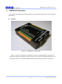
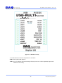
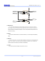
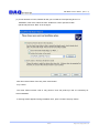
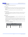
USB-MULTI Users Manual (Rev 1.0) USB-MULTI User’s Manual Windows, Windows2000, Windows NT and Windows XP are trademarks of Microsoft. We acknowledge that the trademarks or service names of all other organizations mentioned in this document as their own property. Information furnished by DAQ system is believed to be accurate and reliable. However, no responsibility is assumed by DAQ system for its use, nor for any infringements of patents or other rights of third parties which may result from its use. No license is granted by implication or otherwise under any patent or copyrights of DAQ system. The information in this document is subject to change without notice and no part of this document may be copied or reproduced without the prior written consent. Copyrights 2005 DAQ system, All rights reserved. -1- http://www.daqsystem.com USB-MULTI Users Manual (Rev 1.0) Contents 1. Introduction 2. USB-MULTI Internal Block 3. USB-MULTI Description 3.1 Outline 3.2 Function Description 3.3 Connector Pin Map 3.3.1 USB Connector Pin-out 3.3.2 D-Sub 25 Pin Connector Pin-out 3.3.3 D-Sub 9 Pin Connector Pin-out 4. Installation 4.1 Hardware Installation 4.1.1 Product Contents 4.2 Driver Installation 5. Sample Program 5.1 Program Interface 5.2 Function Description Appendix A.1 Dimension Reference -2- http://www.daqsystem.com USB-MULTI Users Manual (Rev 1.0) 1. Introduction USB-MULTI has a Digital I/O 15, Analog Input 8, Analog Output 3, Photo-Coupler Isolated Input 2, 16bit Counter 1, 16bit Timer 1, Photo-MOS Relay 1, so use it as interwork with various signals. Full Speed (12Mb / s) USB 1.1 interface board that is used. All of the control board FPGA (Field Programmable Gate Array) is designed as an augmentation or modification free and easy upgrade for user needs. DAQ System Analog I/O Products Analog Input Analog Output Timer Products Sampling Resolution Channel Rate Range(V) Resolution Channel 100Ksps 12/14/16 0~5, 8 Single Ended 0~10 /4 Differential ±5, ±10 PCI-AIO02 100Ksps 12/14/16 0~5, 8 Single Ended 0~10 /4 Differential ±5, ±10 PCI-AIO04 100Ksps 12/14/16 16 Single 0~5, Ended 0~10 /8 Differential ±5, ±10 PCI-AIO05 100Ksps 24/16 0~5, 4 Single Ended 0~10 /4 Differential ±5, ±10 PCI-EK01 200Ksps 12/8 PCI-PID01 52Ksps Range(V) /Counter 2 0~10, ±10 16 8 0~5, 0~10, 0~10.8 ±5, ±10, ±10.8 12 2 0~10, ±10 8 Single Ended 0~3.3, /4 Differential ±1.65 12 4 0~3.3 20 4 ±10 16 1 ±10 PCI-MUL06 256Ksps 16 6 ±5, ±10 16 1 ±10 cPCI-EK01 8 Single Ended 0~3.3, /4 Differential ±1.65 12 4 0~3.3 1/1 10/12 3 0~3.3 1/1 PCI-AIO01 USB-MULTI 200Ksps 12/8 12/14/16 8 0~5, 0~10 ±5, ±10 -3- 12 1/1 http://www.daqsystem.com USB-MULTI Users Manual (Rev 1.0) DAQ System Digital I/O Products Product No. In/Out Timer/Counter Specification cPCI-DIO6400 32/32 Isolated Input/Output cPCI-DIO02 128 channels Software Configurable 16bit단위 8Group로 Read/Write PCI-DIO6400 32/32 Isolated Input/Output PCI-DIO6401 64/None Isolated Input PCI-DIO6402 None/64 Isolated Output PCI-DIO01 32/32 Software Configurable 1/1 TTL Level Input/Output 32bit Counter/Timer PCI-DIO02 128 channels Software Configurable 1/1 16bit단위 8Group로 Read/Write PCI-DIO12 16/16 or 32/32 Software Configurable 128Mbyte DDR SDRAM Data transfer rate up to 400Mb/s PCI-MOT01 24/24 (Isolated) 2 Channel PWM, 2 Channel Encoder, 1 Channel ADC PCI-PWM02 6/12(Isolated) 4 Channel Triggered PWM outputs PCI-TC03 16/16 PCI-EK01 24(shared) PCIe-DIO05 32/32 TTL Level Input/Output USB-AIO10 24/24(Isolated) 4-Ch Analog Input and Output RS-232 115,200bps Interface USB-DIO12800 128 channels Software Configurable 16bit단위 8Group로 Read/Write USB-DIO6400 32/32 USB-MULTI 16/16 USB-PWM10 6/8(Isolated) 8/8 32bit resolution Differential Counter/Timer 1/1(32bit) 12bit 8 Channel A/D Input 12bit 8 Channel D/A Output 1/1 Isolated Input/Output 12Mbps Isolated Input/Output 16bit Counter In & Timer Out 4 Channel Triggered PWM outputs -4- http://www.daqsystem.com USB-MULTI Users Manual (Rev 1.0) It is the device which USB-MULTI product exchanges an external sensor or Autuator or digital signal or analog signal through USB interface at PC. An external signal have Digital I/O 16, Analog Input 8, Analog Output 3, Photo-Coupler Isolated Input 2, 16bit Counter 1, 16bit Timer 1, Photo-MOS Relay 1, so use it as interwork with various signals. An action of a product is controlled by API calls and the following picture is showing by a working together action. [Figure 1-1. USB-MULTI Usage] Figure 1-1 shows, USB-MULTI don’t use an external power separately because power supply to USB cable. -5- http://www.daqsystem.com USB-MULTI Users Manual (Rev 1.0) 2. USB-MULTI Internal Block The total control takes charge of the Micro controller in case of USB-MULTI as like Figure 1-1. Main function is Analog Input/Output, UART data communication and general 16bit Digital I/O. These functions perform to use the API at PC through USB interface. The product gets from 5V power supply through USB interface that converts 3.3V. If it is not an isolated Input, it is a 3.3V CMOS level Input/Output. And it can receipt 5V TTL level in case of input. In other words, it is 5V Tolerant. USB-MULTI USB Interface USB Full Speed Device 1.1 Specification SIE Micro controller 16Bit I/O CMOS 3.3V Level I/O UART Communication Data Photo-coupler input 2Channel Isolated Input Photo-Mos Relay Output 1Ch ADC 8 Channel Isolated Output Analog Signal 16Bit Timer DAC 3 Channel 16Bit Counter [Figure 2-1. USB-MULTI Block Diagram] GENERAL DESCRIPTION ♦ USB 1.1 Specification ♦ Full Speed Device 12Mbps ♦ 8Mbit(1MByte) High Speed SRAM -6- http://www.daqsystem.com USB-MULTI Users Manual (Rev 1.0) APPLICATION ♦ Data acquisition ♦ Laboratory instrumentation ♦ Process control systems ♦ Factory automation SPECIFICATION ▣ Interface ▪ USB Powered through USB-B Connector ▪ +5V Single Power Operation ▪ 24 point terminal for sensor connection ▪ D-sub 25pin female connector for 15 digital I/O ▪ UART(Data bit 8, 1 start, 1 stop, No Parity , 38400bps) Tx/Rx ▣ Function ▪ One 16bit Timer / One 16bit Counter ▪ 8ch 12(14/16)bit ADC / 3ch 10(12)bit DAC ▪ One SSR output ▪ Two photo-coupler isolated Digital input ▪ 16 Digital I/O SOFTWARE ▣ Operating System ▪ Windows 2000 SP4/XP SP1 over ▣ Recommended Software ▪ API : Interface with Application through client DLL -7- http://www.daqsystem.com USB-MULTI Users Manual (Rev 1.0) 3. USB-MULTI Description Each of the product features are briefly described. For more features please refer to the component specifications. 3.1 Outline [Figure 3-1. USB-MULTI Out-side View] Figure 3-1 shows an outside view of USB-MULTI. There is a USB and RS232 connector to the right side. A Digital, Analog Signal connection have a each 12 port to the right/left side which it is to the top side. There are 16 channels Digital I/O through 25PIN D-SUB connector to the left side. -8- http://www.daqsystem.com USB-MULTI Users Manual (Rev 1.0) [Figure 3-2. USB-MULTI View] The board has two LED, each explanation is as follows. PWR : When power start, light on. RUN : If it use a function of product through USB, a product can confirm repeatedly light on/off whether or not running. -9- http://www.daqsystem.com USB-MULTI Users Manual (Rev 1.0) 3.2 Function Description (1) AVDD The power (3.3V) of analog circuit can use external. The maximum current is within 150mA under for using external. (2) AGND It is a GROUND of analog circuit power. (3) ADC0 - 7 It is a analog input from 0 to 7. Currently voltage input range is from 0 to 5V. (It will be upgrade later and can be changeable.) The resolution of analog input is 12 bits, can work 14 bits, 16 bits according to orders. Using ADC chip is LTC1857, refer to specific specification or chip manual of Linear Company. (4) REFOUT It is an output terminal of analog reference voltage (2.5V). You can’t have to use to power from reference terminal. (5) DAC0 - 2 It is an analog output channel from 0 to 2. The range of output voltage is between 0 to 4.75V. (It will be changeable later through Hardware upgrade) The resolution of analog input is 10 bits, can work 12 bits according to orders. Using DAC chip is AD5316A, refer to chip manual of Analog Company. (6) DIN0, DIN1, DIN_COM It is two inputs with photo-coupler isolated and an input common terminal. It has no input polarity. -10- http://www.daqsystem.com USB-MULTI Users Manual (Rev 1.0) VCC DIN_COM Input0 1.5K DIN0 VCC Input1 1.5K DIN1 (7) SSR OUTA, B It is a Photo-MOS Relay(Semiconductor Relay) output port to control the maximum 60V (voltage), 0.5A (current) without AC/DC distinction.(The semiconductor relays have extreme resistance to abrasion and spark, so it is a semi-permanent relay because of no mechanical contact.) (8) CNT IN It is an input of 16bit counter, the counter increase by 1 in case of High to low (Falling edge). (9) TMR OUT It outputs a timer pulse. The pulse width is 50nSEC, period setup is exchangeable timer register. If it is 0xFFFF, the minimum period is 500nSEC (0.5uSEC), If it is 0x0000, the maximum period is 32.748ms (0.5 x 65536 = 32768uSEC). (10) DGND It is a Ground terminal of Digital circuit (Counter, Timer). -11- http://www.daqsystem.com USB-MULTI Users Manual (Rev 1.0) 3.3 Connector Pin Map The board has several connectors to set. There are the USB-B connector for USB communication, the D-sub 25 pins connector for general purpose I/O and the D-sub 9 pins connector for RS232 communication. 3.3.1 USB Connector Pin-out J1 is a USB-B type connector for High speed USB connection. Figure 3-3 and Table 1 shows the J1 connector and its pin description. 2 1 USB B type Connector 3 4 [Figure 3-3 . J1 Connector (USB-B type Front View)] [Table 1. USB-B Connector] No. Name Description 1 VCC 2 D- USB Signal Minus(Negative) 3 D+ USB Signal Plus(Positive) 4 GND Remark USB Power +5V USB Power GND -12- http://www.daqsystem.com USB-MULTI Users Manual (Rev 1.0) 3.3.2 D-sub 25pin Connector Pin-out The digital input/output is through 25PIN D-sub connector (socket type), it is 3.3V CMOS level. But, the port itself is 5V Tolerance, it is compatible a 5V TTL level signal. The connector pin description is as follows. 13 12 25 11 24 10 23 9 22 8 21 7 20 6 19 5 18 4 17 3 16 2 15 1 14 . [Table 2. D-sub 25pin PIN-OUT Description] No. Name Description 1 +5V Board Power(+5V) 2 PB1 Multiplexed Pin PB1 3.3V CMOS Logic 3 PB3 Multiplexed Pin PB3 3.3V CMOS Logic 4 +5V Board Power(+5V) 5 PB5 Multiplexed Pin PB5 3.3V CMOS Logic 6 PB7 Multiplexed Pin PB7 3.3V CMOS Logic 7 +5V Board Power(+5V) 8 PA1 Multiplexed Pin PA1 3.3V CMOS Logic 9 PA3 Multiplexed Pin PA3 3.3V CMOS Logic 10 +5V Board Power(+5V) 11 PA5 Multiplexed Pin PA5 3.3V CMOS Logic 12 PA7 Multiplexed Pin PA7 3.3V CMOS Logic 13 GND Board Digital Ground 14 PB0 Multiplexed Pin PB0 3.3V CMOS Logic 15 PB2 Multiplexed Pin PB2 3.3V CMOS Logic 16 GND Board Digital Ground 17 PB4 Multiplexed Pin PB4 3.3V CMOS Logic 18 PB6 Multiplexed Pin PB6 3.3V CMOS Logic 19 GND Board Digital Ground 20 PA0 Multiplexed Pin PA0 3.3V CMOS Logic 21 PA2 Multiplexed Pin PA2 3.3V CMOS Logic 22 GND Board Digital Ground 23 PA4 Multiplexed Pin PA4 3.3V CMOS Logic 24 PA6 Multiplexed Pin PA6 3.3V CMOS Logic 25 GND Board Digital Ground -13- Remark http://www.daqsystem.com USB-MULTI Users Manual (Rev 1.0) 3.3.3 D-sub 9pin Connector Pin-out The USB-MULTI is having function of a RS232C communication except USB. Currently, the RS232 is use to self-test(38400bps, 8bit data, 1 stop bit, No parity), but it will be upgrade to general serial communication. The connector signal description is as follows. 1 2 6 3 7 4 8 5 9 The connector is the RS232C standard 9PIN (PLUG Type) D-sub connector. [Table 3. D-sub 9pin PIN-OUT Description] No. Name Description 1 N.C. No Connection 2 RxD Receive Data RS232C Receiver 3 TxD Transmit Data RS232C Transceiver 4 N.C. No Connection 5 Ground 6 N.C. No Connection 7 N.C. No Connection 8 N.C. No Connection 9 N.C. No Connection 통신 Ground Remark Ground -14- http://www.daqsystem.com USB-MULTI Users Manual (Rev 1.0) 4. Installation You confirm whether or not the packing contents are in good order before installation. 4.1 Hardware Installation 4.1.1 Product Contents ① USB-MULTI ② USB(A-B) Cable ③ CD (Driver/Manual/API/Sample Source etc.) [Figure 4-1. USB-MULTI Product Contents] -15- http://www.daqsystem.com USB-MULTI Users Manual (Rev 1.0) 4.2 Driver Installation For USB-MULTU board installation to PC is as follows. There isn’t a Jumper to especially to set up for board installation in case of USB boards as it is Plug & Play devices. User environment : Windows 2000 SP4 over, Windows XP SP1 over. (1) First, open the box and put the USB-MULTI product on safe table. (2) The USB-MULTI connects to PC through USB A-B cable. If connected cable, It will be install automatically drive searching at Windows operating system. (3) The driver installation is as follows. The installation order is as follows, explain Windows XP with bases if there isn’t special explanation. -16- http://www.daqsystem.com USB-MULTI Users Manual (Rev 1.0) (4) If new hardware is found, Wizard will ask you to install the corresponding driver. For installation of the driver, select the item “Install from a list or specific location (Advanced)”and click “Next” as in the figure. After find a driver folder of the CD, press “Next” button. ex) F:\driver The driver folder includes a file of “usb_aio01.inf” and “usb_aio01.sys” that it is necessary for driver installation. A warning window appears during installation here, press “Continue Anyway” button. -17- http://www.daqsystem.com USB-MULTI Users Manual (Rev 1.0) (5) If the installation is completely finished, you can use USB-Multi board. But it confirm a driver normally installation in the following ways. Do the following steps to show up the “Device Manager” window. [My Computer -> Properties -> Hardware -> Device Manager -> Universal serial Bus controllers -> “DAQ system USB Multi Function Board” -18- http://www.daqsystem.com USB-MULTI Users Manual (Rev 1.0) 5. Sample Program 5.1 Program Interface A sample program is provided to make the user get familiar with the board operation. Before using it, you have to install the board and its driver in your computer properly. Sample program is provided in source form in order to show the usage of API (Application Programming Interface) of the board and may be modified for customer’s own usages. [Figure 5-1. Sample Program Window] To run the sample application program, you need to use API( Application Programming Interface), which is a form of client DLL. To compile the sample source to make its executable file, you have to use Import Library files and Header files. You can find them in the CDROM. To run the .exe file, the API DLL file(usb_dio6400.dll) must be in the same directory with the .exe file or in Windows system folder. Another method is to add the directory of API DLL file to PATH environmental variable. -19- http://www.daqsystem.com USB-MULTI Users Manual (Rev 1.0) 5.2 Function Description (1) Get Board Info Button It displays current state value of the product (DIO, SSR, DIN, Counter, ADC). (2) Auto Read Check Box Periodically auto read. (3) DIO Function DIO is from 0 to 14bts, each bits can set up input or output. When firstly power up, it is a state of input. The decision of input/output set up to press “Set Direction” button. If each bit position is a state of “1”, it will be output. If each bit position is a state of ‘0’, it will be input. If you want to output of all bits, write “FFFF” at “Set Direction” windiw. If you want to input of all bits, write “0000” at “Set Direction” window. Reading and writing of each port performs press “Read / Write” button. (4) SSR Function It controls to output of Photo-MOS Relay(Semiconductor Relay). When press “SSR ON” button, it will be connected with relay. When press “SSR OFF” button, it will be disconnected with relay. A state of output displays SSR LED. When press “Get Board Info.” button, it will be executed as above processing. -20- http://www.daqsystem.com USB-MULTI Users Manual (Rev 1.0) (5) Photo-coupler DIN It displays a state of Photo-coupler input on LED. (6) Timer Function It controls to output Timer to TMR OUT terminal. When press “Timer Reset” button, it will be stop output. When press “Timer Set” button, it will be continuous display the timer output as setup value. The timer output is 50nSEC High Pulse, period is the minimum 500nSEC (0.5uSEC). (7) Counter Function It counts a number of pulse which was inputted to CNT IN terminal. A maximum value of count is 0xFFFF. When initialization, press “Reset” button. If you want read a current count number, press “Read” button. (8) DAC Function A DAC setup value is as below picture. Bit “1..0” and “15..12” 0 have to be full of “0”, 10bit valid value is only used a DAC setup value. If all bits are “0”, output works “0V”. If the bits are 0x0ffc, output works 5V. But, since the maximum output voltage is approximately 4.75V, output doesn’t increase any more for a certain value of setting. So, if you want to output voltage which you wanted, you can calculate according to way. The resolution is as follows 5V / 0x1000(4096) = 0.00122[V]. If you want 3V output, you have to write 3 / 0.00122 = 2458(0x0999). DAC 15 14 13 12 11 10 9 0000 Setup Value 8 7 6 5 4 10bit DAC Setup Value -21- 3 2 1 0 00 http://www.daqsystem.com USB-MULTI Users Manual (Rev 1.0) (9) ADC Function An input range of ADC is from 0 to 5V. It will be changed a input range to future upgrade. ADC setup value is as follows. ADC 15 14 13 12 11 10 9 Setup Value 8 7 12bit ADC Value 6 5 4 3 2 1 0 0000 The basic resolution of product is connected a 12 bits to upper bits. The lower 4 bits is always read to “0”. (If the resolution is 14bits/16bits, it can use the lower 4 bits.) To read value is exchange real voltage as follows 5V / 0x10000(65536) = 0.000076293[V]. If it reads a value 0x2000, it is 0.000076293 x 0x2000(8192) = 0.625 [V]. (10) ADC Read, ADC Read All Button It displays the input of the current ADC value on screen. In case of ADC Read, it displays each channel values. In case of ADC Read All, it displays all channel values. (11) ADC Graph A value of ADC channel 0 displays on graph, it can set up a value of Offset and Scale. -22- http://www.daqsystem.com USB-MULTI Users Manual (Rev 1.0) Appendix A.1 Dimension The dimensions of the product are as follows: -23- http://www.daqsystem.com USB-MULTI Users Manual (Rev 1.0) References 1. USB 2.0 System Architecture -- Don Anderson, USB SIG(www.usb.org) 2. Universal Serial Bus Specification -- Compaq/Intel/Microsoft/NEC, MindShare Inc. (Addison Wesley) 3. AN201 How to build application using API -- DAQ system 4. AN342 USB-MULTI API Programming --DAQ system -24- http://www.daqsystem.com