1
!ladle IhaeK
•
ervlce
TRS-BO
MINI DISK
Catalog Number 26-1160/1161
CUSTOM MANUFACTURED IN U.S.A. FOR RADIO SHACKl!A DIVISION OF TANDY CORPORATION
TABLE OF CONTENTS
PAGE
1
INTRODUCTION (ASSY 171013 - 0011 •. . ..•.
Power Supply
. .•......•.• .
SECTION I
GENERAL DESCRIPTION
INTRODUCTION
.
Physical Description
. • . . . . . . . . . ..
•.••..•..•
.. ,
Functional DescriptIon
Interface Connections
1
.
.•....
.•••
. . . . . . ..
•.
..
3
. .. . .. . .. .. . ..
3
... . . .•.. .. .. ..
3
. •. .. . •••••. . •. .
. . . . . . . . . . . . . . . . . . . . . ..
3
3
Physical Checkout . ..
..
Mounting the Disk Drive . . . . . . . . . . . . . . . . . . • • • • . . • • • • . . . • . .
3
5
Resistor Termination, DIP Shunt and Jumper . . . . . . • . . . . . . . . . . . . .
Flat Ribbon Cable AS5embly
. . . . . . . . . ..
6
5
SECTION II
THEORY OF OPERATION
Introduction
Organization of the Diu.: Drive
Functional Block Diagram DescriptIon ...
Index
Write Protect
Track GIf Switch
Spindle Drive
Positioner Control
Data Electronics
Data Recording
Data Reproduction
SECTION III
OPERATION
Introduction. .... .. . . . . . . . . . . . . . . . . • . . . . . . . . . . . . . . .
Interface Electronics Specifications ..•..•.....•..
Input Control Lines
. . . . . . . .. .
.
.
Select Lines (NOS' N0S41
.
. .
Drive Motor Enabla (NMOTORONI . . . .. .. .. ...•..•• . •..•
Direction and Step Lines (2 Lines) (DIRI (NSTEP) .......•....•.•
Write Dau (NWRITEDATA) .
. .. .
.
Write Enable (NWRITE GATE) . . . . .
., ............••
Output Status
. . . . . ••
• ••• _ •••••.. _ •..
Index ININOEXISECTORI
. . . . .•
. .• . ...
TrICk GG (NTRK HI
Write Protect (NWRITEPROTECTI
Read DltalNREADDATAI .
7
7
7
7
7
7
7
7
8
9
•
11
11
11
11
11
11
11
11
13
13
13
13
13
TABLE OF CONTENTS (Cont'd)
PAGE
SECTION IV
MAINTENANCE
Physical Description of the PC Boards
., ...
Circuit Board Test Points. .. ... ..
. . • . . . . .. . . . • . . . . . . . .
Option Select . . . . . . . . . . . . . . . . . . . . . . • . . . • . • • . . . . . . . . . . . .
Preventive Maintenance
...............•..•.............
Cleaning the Head. .
. . . . . .. .
. .
ADJUSTMENT
CE Alignment .
Disk Drive Preparation ••••
R~ial TrICk Alignment ••
Index Sensor Alignment
Trade Gil Switch
Write Protect Switches
Drive Motor Speed
15
15
15
17
17
17
17
17
17
17
18
18
PARTS LIST
Mini-Disk Power SuppiV.
..
Disk Controller Board ..
Servo (Motor Controll Board
.
23
. . . . . . . . . .. .
.
. ..•.....••..•....
2'
.
. . . . . . .. .
.
•• . ••...
27
27
27
SECTION V
INTRODUCTION (MINI 25060 - xx)
Resistor Termination, DIP Shunt and Jumper
Flit Ribbon Cable Assembly. . . . . . .
26
LIST OF ILLUSTRATIONS
PAGE
FIGURE
1
2
3
•
5
6
7
8
•
10
11
12
13
"••
(SECTION
15
16
Mini-Disk Power Supply Schem.tic .
PC Board Component locations . . .... ,
Resistor Termin.tion. DIP Shunt and Jumper
• __ • ' ,
Cable Assembly Connector Pin Removal Chart., '. __ • _ , _
Functional Block Diagrem " , . , , . , ,
, , . , ,. .., .. ,
FM Recording
,
, . ..
. . _, . ,
.• _ , . • . . •
• .• ' ..
Write Timing Diagram
,, , ,
Read Timing Diagram
• _ ' .. ' , , ,
.. ' . , .
Interlace Configuration
Circuit Bo.d Test Points.nd Connector locations
Cat's-eye Panern
, • _ • ' . , _.
• • _• ' ,
__ . , .. , • _ •
Index to DaUi
Servo (Motor Control I Board SchematiC "
.••
Mini·Disk Drive Schematic (ShMt 11
Mini-Disk Drive Schematic (Sheet 21
20
21
Resistor Termination, DIP Shunt .rw:I Jumper
Cable Assembly - Connector Pin Removal Chart ..
27
27
1
•
5
5
8
8
10
10
11
16
18
18
I.
VI
TABLE
1
2
3
Mini,Disk Drive Med'lanical and Electrical Specifications.
Interface Connector Pin Assignments, J1/P1
Power Connector Pin Assignment
ii
...
2
12
12
MINI-DISK SERVICE MANUAL
(ASSY 71013 - 001)
INTRODUCTION
This manual provides a General Description of the Mini·
Service information for Drives that have serial numbers
such as MINI25060 - xx can be found in the back ofthis
manual (following the Parts Lists).
Disk Drive System. It also includes: Theory of Operation;
Operation; Maintenance; Schematics; and Parts Lists for
Drives that have Logic PC boards with the serial number
The Power Supply, Case. and external Cables are the same
ASSY171013 - 001.
for both units. The Power Supply Specifications are slightly
different.
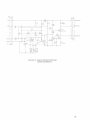
POWER SUPPLY
SPECIFICATIONS
INPUT ....
120 VAC, 60 Hz
OUTPUT III
+12 (ia.B) vae
CURRENT
_ ..
900 rnA (max), 0.75 A (WP)
MAXIMUM RIPPLE
. lOOmVp-p
+5(±0.25) VDC
OUTPUT (2) . . . . . . . . . . . . . • • . . • , .••.....
CURRENT,
600 mA (maxI, 0.50 A (typ)
MAXIMUM RIPPLE, , , .....
50 mV Pi>
NOTE: Refer to Section V - Output (1) current is rated
at 1.50 A (maxI. This value occurs only during
Head Loading and lasts approximately 200 ms.
r------------------------------,
~~[~T
I
I
I
CIl'
IN4002
I
r--"
I
_
K
:
- IWNTl
'II
I
I
I
I
I
I
I
I
~~"
""
CIl~
(
12:0 ....C
60 HZ
I
I
CII
12 IilCIT23CP
II
II
'0
k.J; h
2
~ ~1~~/2W 1 PI
a:101W1!'~~.I1rbrilJ·,.t=I"i~-t_;_lr"~ill
CIl5~·
['u
C114
IN4002
4 15
Ii'-
15K
g~ool
112
u
10K
22K
.12V
I
•
:
l i ~-----J-ll--..'::====~~~;::JiI~: ~ il
IIIEO I
01
K~1l1
'--
"
I~T
ti...I ,;~S,?o;;----r;:::=_-i
I ''''1-,,05
" '"
."
C
'Ii'
:GIlN
I
IL
1111002
•
"'
i
33K
L--'---L4-12
I
12V IlETuIlN
•,.~;o. '----+--14.5
I
I
V
!
L------'------'-----'-------4
,-{oJ~ 'VUTUIlN
~
w.u
UNLtU OTIlfl!WI5E SPECIfiED
,
" ,, •" ,,,
• ""
•
• '00'
- •, "•
"
~
CUIlIlENT LIIIIIT
CUllllEffT .[~[
INV INPUT
NON ·IHY INPUT
V liEF
I .LL IlESISTOIIS olliE 1/4 WUT, " ,
Il[SISTOII V.LUES IN OHIilS,lloI000
2 C.P.C,TOfI V.LI.IES IN "'IClIOf.Il.0S
.litO WOlllllNG VOLUGE
3 -lltOICUES Cl,.OCIlWISE 1I0UTlOfrI
V«_
FlIt:O CO/IlP
~
~
IilCI123CP TQPVlEW
FIGURE 1. MINI-DISK POWER SUPPLY
SCHEMATIC.
1
Industry-eompatible 5·1/4 inch (133.4 mm) diskette
48
Number of Tracks
Re.d/Write TrICk Width
Dimensions
Hei\tlt
Width
35
9.912 inches (252 mml
3.38 inches (85.85 mml
5.87 inches (149.10 mml
8.0 inches (203.2 mml
4.5 Ibs (2.04 Kg
0."'"
Wetght
Temper~u,..
(Exclusive of M.cii.1
Oper.ting
Non-oper.ting
l00c to 4JOe (500F to 11l)OF)
-4(JOC to 110C I.....OOF to 16()OFI
Rel.tive Humidity
(Exclusive of Medi.)
Oper~ing
Non--opeuttng
20% to 80%
5% to 95'10 (non<:ondensing)
6 to 600 Hz 0.5g oe.k
Seek Time
5 msec tr.ck to track
Error R.te
1 per 109 recover.ble
1 per 10 12 noo-r8Coyer.ble
20,000 hours (norm.1 use)
M.cii. Life
3 million p.sses on • single trICk
Disk Speed
300 rpm.:!:1.5% (long term)
~3.00{,
Start!Stop Time
250 msec (m.ximum)
Tr.nsfer Rlt.
125/250K bits/sec
BiUlDiSk (unformmed)
1.75 million (FM)
Aecording Modes (typic.U
FM, MFM, MMFM
Power
+12 V dc!:.0.6 V, 9OOm. m.ximum
5 V dc!:.0.25 V, 600 m. muimum
TABLE 1. MINI-DISK DRIVE MECHANICAL
AND elECTRICAL SPECIFICATIONS.
2
SECTION I
GENERAL DESCRIPTION
INTRODUCTION
The Disk Drive is a "MIN I" Disk Memory designed for ran-
The Drive is also supplied with the following sensor systems:
1.
dom access data entry. storage, and retrieval applications.
These applications typically, are intelligent terminal control-
2.
lers, micro-computers, word processing systems, data com·
munications systems, error l099ing, micro-program loading
and point-of·sale terminals. The Disk Drive is capable of reo
cording and reading digital data using FM, MFM or M2FM
techniques.
3.
PHYSICAL DESCRIPTION
The electronic components are mounted on two PC boards:
the Logic board· located above the chassis and the Servo
board· mounted at the rear of the Unit. Power and Interface
signals are connected directly to the Logic board (Figure 2).
The spindle is belt driven by 8 DC motor with an integral
tachometer. The servo control circuit, pulleys and the
tachometer control the speed of the spindle. The read/write/
erase head assembly is positioned by means of a stepper
motor, split band and a pulley.
FUNCTIONAL DESCRIPTION
The Disk Drive is fully self-contained. It consists of a spindle
drive system, a head positioning system, and read/write/erase
system.
When the front latch is opened, access is provided for the
insertion of a 5.25 inch (133.4 mml standard diskette. The
diskette is positioned in place by plastic guides, the front
latch and a back stop.
A track 00 switch which senses when the Head/
CarriaQll assembly is positiooed at Track 01.
The index sensor(an LED light source and a phototransistor) is positioned so that when an index
hole is detected, a digital signal is guaranteed. The
index sensor used is a high resolution device which
can distinguish holes placed close together, i.e., in·
dex-sector holes in a hard sectored diskette.
The write-protect sensor disables the Disk Drive
electronics whenever a write·protect tab is applied
to the diskette.
INTERFACE CONNECTIONS
Signal connections for the Disk Drive are made via a usersupplied 34·pin flat ribbon connector (3M Part Number
3463-001 or equivalent). This connector mates directly
with the PC board connector lJ1) at the rear of the Drive.
The DC power connector is a four-pin connector (J2) which
is keyed to mate with the connector on the Logic PC board
at the! top rear of the Drive.
The signal COflnector harness should be of the flat ribbon or
twisted pair type with the following chlfacteristics:
1.
2.
Maximum length of 10feet(3M).
22· 24 gauge COflductor compatible with the connector to be used.
Power connectiOfls should be made with 18 AWG cable
minimuml.
PHYSICAL CHECKOUT
Closing the front latch activates the cone/clamp system
which centers and clamps the diskette to the drive hub.
The drive hub is driven at a constant speed of 300 rpm by a
servo controlled DC motor. In operation, the magnetic head
is loaded into contact with the recording medium whenever
the front latch is closed.
A 4-phase stepper motor/band assembly and its associated
electronics position the magnetic head over the desired
track. This positioner employs a one·step rotation to cause
a l-track linear movement. When a write-protected diskette
is inserted into the Drive, the write-protect sensor disables
the write electronics of the Drive and an appropriate signal
is applied to the interface. lWhen performing a write opera·
tion, a O.013·inch (0.33 mm) [nominal] data track is recorded.)
When performing a write operation, a 0.013-inch (0.33 mm)
[nominal) data track is recorded.
Before applying power to the unit, the following inspection
should be performed:
1.
2.
3.
4.
5.
Front latch. Check that the front Iltch opens and
closes. Note that when the door is opened, the
head arm raises.
Ensure that the front panel is secure.
Manually rotate the drive hub. The hub should
rotate freely.
Check that the PC boards are set:ure. Check that
the connectors are firmly seated.
Check for debris or foreign material between the
heads and remove same.
NOTE: To ensure proper operation of the Drive, the chassis
should be connected to earth ground. The 3/16·inch
14.76 mm) male ac lug, located at the rear of the chassis, is
provided for this connection.
Data recovery electronics include a low-level read amplifier,
differentiator, zero-crossing detector and digitizing circuits.
No data decoding facilities are provided in the basic Drive.
3
..
,
, e4'
10 u,,..
,
•
'"
..••II ".
~.u!
II "'0
--- Jill
...
•
............
--- ,f ]o"II!!f
]
t!ll:
• •
_uo_ •
.....
,
I
III
I '"
• GQ iT " ....~ •
"
-;(j ~oO
.1 j j ' I II .f
] :[
] 'f ]
~
.i ii Q"7f ~
11..I
_u
~ .~~~
lil!1 '"
lIlIlIlI
__
!l
-e..
_11_
_ n,_
."
«-
15!1
-_
<~
I
UlI-
'H •
.
-111-
-In10 u...
•
'2eu
•
,~
...
::: ~
}
xf
]
III (I'.
~
<U
:f
]
1_e~:.t
...
'"
....- :.Q
_u._ "" 'f ] ".
~-IOU'"
•
,•I
I
"'H
<~
.~ '" }
];·f
·f
on
,f
]":f•
.. ,
If
]
.
:f
,
m
.,-;~
"
U•
]
-In-
"
'"
1II(1~'
]
}
_AO.
.. -~
_"0_
{
-1.'-
, ••
,
-n.-
_IU_
"
..
, -,,,
<U
_..- .." - f '"-u.- ~ ... " •
] _.n_ ;
]'' 13 ,,, '" '"
,. • '"
.
II
ql
1P.
"
]
_nl_
ell'
•
• 10III eno
]-
_In_
_IU_
'"
"
] x[
III u"
-lU_
_no-
,•
~u_
II'
I .,.1 •• 0 '
I
• 'H • 1
I
.
I , .u
~
~
n
'"
" ,,..------..,,
,
,
.
_-----~
LOGIC BOARD (COMPONENT SIDE)
0
0
0
0
~te---:
o.
K
0
o-!
""
..R4 Sl'INOt E
SPEEO CONTROL
o.
•
SERVO JUMPER
0
:
0
0
0
o.
SERVO BOARD (COMPONENT SIDE)
FIGURE 2. PC BOARD COMPONENT LOCATIONS.
4
ORIVE MOTOR
MOUNTING THE DISK DRIVE
The Drive can be mounted in any plane, i.e. upright, hori·
zontal or vertical. However, when it is mounted horizontally, the logic PC board side of the chauis must be the
uppermost side. Tapped holes are provided in venous loca·
tions for the attachment of user·supplied hardware.
RESISTOR TERMINATION, DIP SHUNT AND JUMPER
(S.. Figure 3).
1. The Resistor TerminatIon in the IC socket is used in
Drive number zero only. It must be removed for Drives
one. two and three.
2. The DIP Shunt package is used in all Drives and must
be punched and seated as illustrated.
NOTE: Some logic PC boards will not have a DIP Shunt in
the Drive Select circuit. These boards have been redesigned
and the Drive Select circuit is etched into the board.
3. The Jumper Wire between pin 32 of Jl and the DS4
connection (~ Figure 5) is used on ,II Drives.
NOTE: Some Logic PC boards will not have the Jumper
Wire. The connection will be etched into the board.
I IIlJlUOII HIIMINATION
UOi SOClIlTl IIl..oYl (l(
~:;~ .O~.,r:T--"',
"u__.J:J
"
J ~1I.'lIl AOOt:O
-------rTO ALL DIUV(S'
.•
•,•
·'f AI'f'L~f
FIGURE 3. RESISTOR TERMINATION. DIP SHUNT
AND JUMPER.
FLAT RIBBON CABLE ASSEMBLY hee Figure 41.
Pms must be removed from Dnve connectors on the Cable
Assembly as follows and as illustrated'
3. Connector for Drive number two - pins 10, 12 and 32.
4. Connector for Drive number three -
1. Connector for Drive number zero - pins 12, 14 and 32.
2. Connector for Drive number one - pins 10. 14 and 32.
00 not remove any pins from the connector to the EKpan·
sion Interface.
CAlVE
NUM8ERZERO
DRIVE
NUM8ERDNE
DRIVE
NUM8ER TWO
CRIVE
HUMaER THREE
"
"
"
"
"
"
"
"
"
"
pins 10, 12
and 14.
"
"
FIGURE 4. CABLE ASSEMBLY - CONNECTOR PIN
REMOVAL CHART.
5
(Page Intentionally Left Blank)
SECTION II
THEORY OF OPERATION
INTRODUCTION
The Disk Drive consists of the mechanical and electrical
components necessary to record and read digital data on a
diskette. DC pelNef at :!: 12 V and +5 V lprollided by the
strikes the Index Phototransistor c...sing it to oonduct. The
signal from the Index Phototransistor is passed to the Pulse
Shaping Network which produces a pulse for each hole detected. This pulse is presented to the user on the INDEX
PULSE interface line.
user) is required for operation.
WRITE PROTECT
ORGANIZATION OF THE DISK DRIVE
AU electrical subassemblies in the Disk Drive are constructed
with leads which terminale in 4 or 5 pin connectors, enab'ing the individual assemblies to be removed
The magnetic head is connected to the PC board via a cable
terminating in a 5·pin female connector and its associated
male socket which is located in dose proximity to the read!
write data electronics.
A Write Protect signal is provided to the user system vi. the
WR ITE PROTECT interface line. The write protect circuitry
oonsists of • Write Protect Sensor and circuitry to route the
signal produced.
When a write protected diskette is inserted in the drive, the
sensor is activated and the logic disables the write electronics and supplies the status signal to the InterfKe.
TRACK" SWITCH
Interface signals and power are provided via connectors at
the rear of the Drive. A detailed description of these signals
is presented in Section lit of this manual.
FUNCTIONAL BLOCK DIAGRAM DESCRIPTION
The level on the TRACK 00 interface line is a function of
the position of the magnetic head assembly. When the he.d
is positioned at Track 0G and the stepper motor is at the
home position, a true level is generated and sent to the
user.
Figure 5 is a functional block diagram of the Disk Drive and
should be referred to in conjunction with the following
discussion:
SPINDLE DRIVE
The Disk Drive consists of the following functional groups:
The Spindle Drive system consists of a spindle iilssembly
driven by a DC motor·tachometer combination throu~ ,
drive belt,
... Index Pulse Shaper
... Write Protect Sensor
... Track 00 Sensor
Associated with the spindle drive motor are the servo electronics required for control.
... Carriage Position Control
The control circuitry also includes a current limiter and an
interface control line. When the DRIVE MOTOR ENABLE
interface line is true, the drive motor is allowed to come up
to speed. When the current through the drive motor exceeds
1.3 A, the current limit circuitry disables the motor drive,
... Write/Erase Control
POSITIONER CONTROL
... Read Amplifier and Digitizer
The Head Positioning system utilizes, four-phase stepper
motor drive which changes one ph.se for each track .c:t.
vancement of the ReadtWrite carriage. In addition to the
logic neceuary for motion control, a gate is provided as an
element for inhibiting positioner motion during a write
operation.
... Spindle Drive Control
INDEX
An index pulse is provided to the user system via the
INDEX PULSE interface line. The index circuitry consists
of an Index LED, Index Phototransistor and a Pulse Shaping
Network. As the index hole in the disk passes the Index
LEDlPhototransistor combination, light from the LED
7
~.-
I
,
!
.
-.. .
.""'
t--".
-
~
T
""'11 WIT
.... -., "1-- - - - - - ....
,~
"n
FIGURE 5. FUNCTIONAL BLOCK DIAGRAM
DATA ELECTRONICS
AI; signals required to control the data electronics are pro·
vided bv the user system and are shown in the Block D,agram (Figure 5). These control signals are
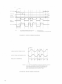
InformltlOfl can be recorded on the diskette using a double-frequency code. Figure 6 illustrates the magnetization profiles in Heh bit cell for the number sequence shown.
The erase gaps provide an erased guard band on either side
of the recorded track. This accommodates the tolerances
in track positioning.
*
SELECT
*
WAITE ENABLE
*
WRITE DATA
The READ DATA composite signal is sent to the user
system via the interface.
~
•• , ...nl_"
_,n.,.,.·"
......." ,..
,,•
,
liT 'Hl
•
,,C<,
,,
too.~ n
~~
I
,
1
•
•
•
,•
~
V,
--.l..
I
I
:
I
" , ' : '~
:
:
:
:
I
,
,
:
"_">C:I,.,,"~n~oO?C
~L...±:....-C
, , ,"
,
,
FIGURE 6. F M RECORDING
8
DATA RECORDING
Referring to Figure 5, it can be seen that the Write Electronics consists of a Write/Erase Current Source and Write
Waveform Generator, Erase Current Source and Trim Erase
Control Logic_
The read/write winding on the magnetic head is centertapped_ During a write operation, current from the Write
Current Source flows in alternate halves of the winding
under control of the Write Waveform Generator.
Before recording can begin, certain conditions must be
satisfied. The conditions required for recording (i.e., unit
ready) must be established by the user system as follows:
(1) Drive
speed stabilization. This condition will
exist 250 mSec after starting the drive motor.
(2) Subsequent to any step operation, the positioner
must be allowed to settle. This requires 20 mSec
total after the last step pulse is initiated, i.e.,
5 mSec for the step motion and 15 mSec for
settling.
NOTE: All of the foregoing operations can be overlapped,
if required.
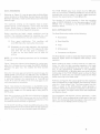
Figure 7 shows the relevant timing diagram for a write operation. At t - 0 when the unit is ready, the WRITE ENABLE
interface line goes true, this enables the Write Current
Source.
Since the trim erase gaps are behind the read/write gap, the
TR 1M ERASE control goes true 390 .uSec after the WR ITE
ENABLE interface line. It should be noted that this value
is optimized between the requirements at Track r;J0 and
Track 34 so that the effect of the trim erase gaps on previous information is minimized.
The TRIM ERASE signal must remain true for BOO pSec
after the termination of WR ITE ENABLE to ensure that all
recorded data are trim erased. This value is again optimized
between the requirements at Tracks 00 and 34.
The duration of a write operation is from the true-golOg
edge of WRITE ENABLE to the false-going edge of TRIM
ERASE, This is indicated by the internal WRITE BUSY
waveform shown.
DATA REPRODUCTION
The Read Electronics consists of the following:
•
Read Switch
•
Read Amplifier
•
Filter
•
DiHerentiator
• Comparator and Digitizer
The Read Switch is used to isolate the Read Amplifier from
electrical signals across the magnetic head during a write
operation.
Before reading can begin, the Drive must be in a ready condition. As with the data recording operation, this ready
condition must be established by the user system. In addition to the requirements established in the paragraph,
DATA RECORDING, a 100pSecdelay must exist from the
trailing edge of the TR 1M ERASE signal to allow the Read
Amplifier to settle after the transient caused by the Read
Switch returning to the Read mode.
Figure 7 also shows the information on the WRITE DATA
interface line and the output of the Write Waveform Generator which toggles on the leading edge of every WRITE
DATA pulse.
Referring to Figure B, the output signal from the read/write
head is amplified by a read amplifier and filtered to remove
noise by a linear phase Filter. The linear output from the
Filter is passed to the Differentiator which generates a
waveform whose zero crossovers correspond to the peaks of
of the read signal. This signal is then fed to the Comparator
and Digitizer circuit.
Note that a minimum of 4 ¢iec and a maximum of 8 pSec
between WRITE ENABLE going true and the first WRITE
DATA pulse is only required if faithful reproduction of the
first WRITE DATA transition is significant.
The Comparator and Digitizer circuitry generates a 1 pSec
READ DATA pulse corresponding to each peak of the read
signal. This Composite Read Data signal is then sent to the
user system via the READ DATA interface line.
At the end of recording, at least one additional pulse on the
WR ITE OATA tine must be inserted after the last significant
WR ITE DATA pulse to avoid excessive peak shift effects.
9
,
..
.,
"" '
,
_.--
...... 'I
,L..---.J
-,
-t--~...-\
I
;
r
:~
..
--.-..
"
I
........-000
I
r'r---i
........, I ---
.-1
_u
----,, --- --,;'---+I
__- ."...-_.-
--...........
fT_.. 010
~
80 ........ .,..
I
----,._-.I
• ......... '0 .....
FIGURE 7. WRITE TIMING DIAGRAM.
• NOTE 1
LlNE"R OUTPUT FROM Fll..TER
OUTPUT FROM OlFFERENTIATOA
READ DATA INTERFACE
t
,·0
NOTES
,.O.2l\O MILLISECONDS AFTER DRIVE MOTOfl STARTS,
0fl20 MILLISECONDS AFTER STEP COMMAND. OR
100 u SECONDS AFTER TEflIl,UNATION OF WAITE
BUSY. !WHICHEVER IS THE LATEST TIMEI
FIGURE 8. READ TIMING DIAGRAM.
10
SECTION III
OPERATION
INTRODUCTION
DRIVE MOTOR ENABLE (NMOTORON)
This section conuins the interfaa description and the eleetrialadiustments necessary for the Disk Drive
When this signal line logiC level goes true (low), the drive
motor KCelerates to its nomin.1 speed of 300 rpm and stab·
ilizes in leu th.n 250 mSec. When the logic level goes false
(high), the Disk Drive deceler.tes to a stop.
INTERFACE ELECTRONICS SPECIFICATIONS
All interface signals are TTL compatiblt. logic true (low) is
+0.4 V (maximum!. Logic false (high) is +2.4 V (minimum).
..
Figure 9 illustrates the interface configuration.
....
•,
,
_.... .-
--------.
"""'...... ,
--,. , ...
".',
: ..<
..
DIRECTION .nd STEP lines (2 lined (DIRI (NSTEP)
When the Disk Drive is selected, a true (low) pulse with a
time duration greater than 200 nSec on the STEP line initiates the access motion. The direction of motion is deter·
mined by the logic state of the DIRECTION line when I
STEP pulse is issued. The motion is towards the center of
the disk if the DIRECTION line is in the true (tow) stlte
when a STEP pulse is issued. The direction of motion is
IWily from the center of the disk if the DIRECTION line
is in the fahe (high) state when a STEP pulse is issued. To
ensure proper positioning, the DIRECTION line should be
stable 0.1 ~Sec (minimum) before the trailing edge of the
corresponding STEP pulse and remain st.ble until 0.1 pSec
.fter the tr.iling edge of the STEP pulse. The ICCflS motion
is initi.ted on the trailing edge of the STEP pulse.
FIGURE 9. INTERFACE CONFIGURATION.
WRITE DATA (NWRITEDATA)
It is recommended that the interface cable be. flat ribbon
cable, with I characteristic impedance of 100 ohms. (or
equivalent twisted pairs) Maximum interf.ce cable length
is 10 feet 13 MI.
Interface connector pin assignments and power connector
When the Disk Drive is selected. this interface line provides
the bit serial WRITE DATA pulSl!!s that control the SWItch·
ing of the write current in the head. The write electronics
must be conditioned for writing by the WRITE ENABLE
line (refer to theWRITE ENABLE paragraph below).
pin assignmentslr. given in Tabl. 2 and Table 3.
INPUT CONTROL LINES (see Table 2)
For elch high-to-Iow transition on the WRITE DATA line,
a flull: change is produced at the head write gap. This causes
a flux change to be stored on the disk.
SELECT LINES (NOSl - NQS4)
The SE LEeT lines provide a means of selecting and deselecting • Disk Drive. These four tines (NOS 1 NDS3 are standard, NDS4 is optional) select one of the four Disk Drives
attached to the controller. When the signal logic level is
true (low), the Disk Drive electronics .re activated and the
Drive is conditioned to respond to step or reKt/write commands. When the logic level is fatSl!! (high). the input control
lines and output status lines are disabled,
A SELECT line must remain stable in the true (low) state
until the execution of a step or read/write command is
completed
The Disk Drive address is determined by SELECT lines 1
through 4 (or a DIP Shunt in the 1E position) on the PC
board These lines provide a means of daisy-chaining a
maximum of four Disk Drives to a controller. Only one hne
can be true (Iowl at a time. An undefined operation might
result if two or more units are assigned the same address or
if two or more SELECT lines are in the true (low) state
simultaneously,
When the double-frequency type encoding technique is
used (in which data and clock form the combined Write
Data sign.I), it is recommended that, when writing all
zeroes, the repetition rate of the high·to-Iow transitions be
equal to the nominal data rate, ±O.l%. The repetition r.te
of the high-ta-Iow transitions, when writing all ones, should
be equal to twice the nominal dati rate. ±O.l%.
WRITE ENABLE (NWRITE GATEI
When this si~al is true (lowl, the write electronics are prepared for writing data (read electronics disabled) This
sign.1 turns on write current in the read/write head. Data is
written under control of theWRITE DATA mput line. It is
generally recommended th ... cha09!s of state on the
WRITE ENABLE line OCC1Jr before the first WRITE DATA
pulse. However. the separation between the leading edge of
WRITE ENABLE and the first significant WRITE DATA
pulse should not be leu than 4 ~Sec and not greater than
8 ~Sec. The same restrictions uist fl)( the relationship be·
tween the least significant WR ITE DATA pulse and the
11
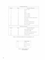
Controller-to~isk
Ground
DrIve
Signal
Description (Mnemonic)
1
2
Connector clamp
3
•
(Spare)
•
5
(Spare)
9
10
SELECT 1 (NOSH
11
'2
SELECT 2 (NDS2)
13
15
,.
I.
SELECT 3 (NDS31
DRrVE-MOTOR ENABLE (NMOTORON)
17
18
DIRECTION
19
20
STEP (NSTEP)
2'
22
WRITE DATA (NWRITEDATA)
23
2.
WRITE GATE (NWRITEGATE)
31
32
SElECT 4 (NDS4)
Disk OrRie-to-ControUer
Ground
Signal
Description (Mnemonic)
7
8
25
26
TRACK GO (NTAK00)
27
28
WRITE PROTECT (NWRITEPROTECTI
29
30
READ DATA (NREAOOATA)
33
34
Connector Clamp
INDEX (NINDEXISECTOA)
TABLE 2. INTERFACE CONNECTOR PIN ASSIGNMENTS. JlIPl
Pin
Supply Vottage
+12 V DC
2
Return (+12 V DC)
3
Return (+5 V aC)
•
+5
vac
TABLE 3. POWER CONNECTOR
PIN ASSIGNMENT
12
termination of the WAITE ENABLE signal When the
WR tTE ENABLE line is false (high), all write electronics
are disabled.
When a write protected diskette is installed in a Disk Driye.
the write electronics.re disabled irrespective of the state of
the WA ITE ENABLE line
OUTPUT STATUS fsee Table 21
INDEX ININDEX!SECTOAI
The INDEX sIgnal is provided once ead'l reYolution (200
m&tc. nominal) to indicate to the controller the beginning
of a track. The INDEX line remains in the true (low) state
for the duration of the INDEX pulse. The duration of an
INDEX pulse is nominally 4.0 mSec.
The leading edge of an INDEX pulsa must always be used
to ensure diskette interchangeability between Disk Drives.
TRACK" (NTRKH)
When the Disk DnYe is selected. the TRACK 110 interface
signal indicates to the controller thlt the read/write head is
positIOned at Track 80 The Track 00 remains true (lowl
until the head is moved away from Track IN.
WRITE PROTECT (NWRITEPROTECTl
When the Disk Drive is selected, this signal line logic leYel
goes true (lowl when the diskette is write protected. The
write electronics are internally disabled when the diskette
is write protected.
NOTE: It is recommended that the write data line be inactive whenever Write Enable is false O.e .. read state).
When the level on this tine is false (high!. the write electronics are enabled and the write opention can be performed. It
is recommended thu the controller not issue • write com·
mand when the WRITE PROTECT signal is true (low).
READ DATA (NREADDATA)
This interface tine transmits the read back data to the con·
troller when the Driye is selected. It provides a pulse for
each flux transition recorded on the medium. The READ
OATA output line goes true Howl for a duration of 1 ¢)ec
for each flux change recorded.
The leading edge of the READ DATA output pulse represents the true positions for the flux transitions on the diskette surface
13
(Page Intentionally Left Blank)
SECTION IV
MAINTENANCE
PHYSICAL DESCRIPTION OF THE PC BOARDS
The Logic PC board is approximately 6 inches (152 mm)
long by 5.5 inches (139 mml wide. Figure 10 illustrates the
placement of test points and connectors.
CIRCUIT BOARD TEST POINTS
The following t85t point description assumes that the Logic
and Servo p.e. boards are installed in the Drive and that the
Drive is in an operational mode with a diskette installed
Logic Ground (TP6)
Step Pulse1TP12)
When stepping in or out, the signal is a high going pulse
for each step of the carriage.
Write Protect Switch (lpg)
When a write protected diskette is installed in the Drive,
the signal is high.
OPTION SE LECT
Input Line Terminations
Digital Logic ground is referenced at TPS,
Differentiated R•., Signal (TP3, TP4)
These t,st points are provided to observe the differentIal output of the second stage amplifier and differentiilted rud signal
The Disk Drive has been provided with the capability of
terminating the input lines listed below:
• MotorOn
•
Read alta Sir98 Shot (TPS)
The output of the single shot used in the read section is
nominally 1.0 IMc for each flux transition detected.
Direction Select
• Step
• Write Data
Ind•• Pulse (TP7)
With I standard soft sectored diskette installed, the
signal is a high going pulse, nominally 4,0 msec in dura·
ation every 200 msec.
Amplified Read SigneilTP1, TP2)
These test points are provided to observe the differ·
ential output of the first stage of read signal amplifi
cation.
Motor On ITP13)
This signal is low true for the "motor on" condition_
Track ,It (TPS)
This signal is low true when the carriage IS positioned
at tr.ck G0 and the step motor phase is correct.
Analog Ground ITP10)
The analog ground reference POIMt
measuring read/write waveforms.
IS
• Write Gate
These lines are terminated through a , 50 ohm resistor pack
installed in a DIP socket located at IC location 2F.
In a single drive system (Catalog Number 26·11'60) this
resistor pack should be kept in place to provide the proper
terminations.
In a multiple drive system (Catalog Numbers 26-' 160 and
one to three 26·1161's) only the last drive on the interface
is to be terminated. All other drives on the interface must
have the resistor pack removed. Catalog Number" 26-1160 is
shipped with the termination resistor installed. Catalog
Number 26-1161 is shipped without a resistor pack.
provided for
15
o
•<%
J3 REAO WHITE
HEAD CO,,"E('TOA
T::::=::l:llll
.
T'7
e
'---J
o
T'IO
T'3
e
o
e
TERU1~ATOR
SOCKET
12F I
T~12
.
e
'"
y
a
eTI":'
'''.CJ]
%
.u.u"o
U
1 0 INTERFACE
Jl INTERFACE
CONNECTION
/
CO"~ECTION
•
!
.,u•
..
••zo
co
••
,
••x
u
••<
X
•0
.,
-0
"
LOGIC BOARD (COMPONENT SIDE)
/-
o
I
o
R~ SP'''Dl(
SPEED CO"lTR(
SERVO BOARD (COMPONENT SIDE)
FIGURE 10. CIRCUIT BOARD TEST POINTS
AND CONNECTOR LOCATIONS.
16
"
~
~[ 1=
$!RVO J(.j'M'ER
{
DRIVE "'OTOR
I
1=
I--
PREVENTIVE MAINTENANCE
To ensure mlft the Disk Drive operates 1ft its design potential, the only scheduled preventive mlfintenance required is
periodic cleaning of the magnetic recording head.
Mechanical and electrical adjustment details are provided
for further service as a result of disassembly or repair.
CLEANING THE HEAD
To clean the magnetic head, u. a lint· free cloth' orconon
swab moistened with 91% Isopropyl alcohol Wipe the head
carefully to remove III accumulated oxide and dirt. Dry the
head using a lint-free cloth.
CAUTION: Rough or abrasive cloth should not be used to
clean the magnetic recording head. Use of cleaning 50lvents
other than 91% Isopropyl alcohol may damage the head.
Extreme care must be exercised to prevent the heads from
being damaged fi.e scratching. banging together, etc.).
ADJUSTMENT
2. Follow the instructions that came with the CE
Diskette.
3. Manually rotate the cam at the rur of the module
until the cilt's-eye pattern, shown in Figure 11, is
observed. Carefully rotate the cam until the cat's-eye
pattern has equal amplitudes.
4 Secure the module by tightening the three retaining
screws that were previously loosened.
5 After securing the module screw, verify Step 4.
Repeat
IS
requirlKf.
INDEX SENSOR ALIGNMENT
1. Pos.ition the Index sensor to the center of travel;
lightly tighten the retaining screw.
2. Perform the CE alignment IS required to locate the
cat's-eye pattern {refer to RADIAL TRACK ALIGN·
MENT above).
3. Perform fifteen step out commands to position the
carriage to Track 01
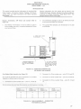
CE ALIGNMENT
The CE alilJ'lment procedure locates the magnetic read/write
head at the proper radial distance from the hub centerline,
thus assuring accurate track location. This adjustment is
necessary only after service, or for suspected diskette inter·
change problems.
DISK DRIVE PREPARATION
Apply the necessary power and control to tum on
the Disk Drive
2. Insert a CE Alignment Diskette fDysan Plfrt Number
224·2A or equivalent) Into the drive and close the
front latch
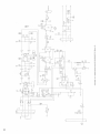
4. Set the oscilloscope horizontal time base to 50 ¢jec
per division.
5. Referring to Figure 12, adjust the photo transistor
mounting block until the first transition of the
2 mSec bunt recorded at Track 01 occun 200:!:50
~c after the leading edge of the index pulse. Adjustment may be made with the use of • flat ·b'aded
screwdriver pl.ced between the photo transistor
mounting block and the Cone Lever as required.
6. Secure the retaining screws on the photo transistor
mounting blocks .nd verify the bunt location. Readjust as necessary
TRACK" SWITCH
3. Attach oscilloscope probes to test points TP1 and
TP2. Place the grouncl clip of the signal probes to
TP10. Adjust the oscilloscope to read diHerentially
fA + B with B inverted). Sync the oscilloscope on
the leading edge of the Index pulse at TP7 with the
5ync probe ground clip at TPG.
RADIAL TRACK ALIGNMENT
Loosen (do not remove) the two module retaining
screws on the bottom of the chassis and the one at
the top rear of the module.
Apply the necessary power and control to turn on
the Drive
2. Insert the CE Alignment Diskette into the Drive and
close the front latch.
3. Position the carriage to the radial alignment trICk.
Confirm the position by observing the cat'nye
pattem.
17
4. If adjustment is required. remove the CE Diskette.
Loosen the retaining screw on the base of the Track
011 bracket, retighten slightly to provide some friction on the bracket and rotate the Track Ge Adjust·
ment Screw (at the rear of the chassis) counter·
clodcwise as far as it will go without forcing it.
5 Position the carriage to Track ", by performing
repetitive step out pulses.
6. Rotate the Track GO Adjustment Screw clockWise
very slowly - until the switch "clicks" Then rotate
the screw clockwise hame direction) exactly one
half turn.
4 Adjust the switch by loosening the retaining screw,
removing the switch assembly and setting the switch
higher or lower as required.
DR IVE MOTOR SPEED
Apply the necessary power and control to turn on
the Drive.
3. Ensure that the Drive Motor Enable line is active.
WR ITE PROTECT SWITCHES
Insert a non·write protected diskette partially (half·
way) into the Drive.
.
"'_
3. Insert the diskette fully against the diskette back
stop rid close the front latch. Ensure that the
switch is deactivated.
2. Insert the Diskette.
7. Tighten the retaining screw previously loosened.
."., ...."
2. Ensure thlt the switch is actuated.
4 Adjust the Speed Control potentiometer (on the
Servo board) until the tIming disk is stationary in
fluorescent lighting.
.
~
v
FIGURE 11. CAT'S·EYE PATTERN.
I
I
."
FIGURE 12. INDEX TO DATA
18
.......
0" .... 0 ......
_12'\1
I.[
,,
",
,."
• TACH
'"
"'
,
"
HI.. I'lli
,,- - - - -
~
1
~
LMl1IUP<
"
- -
,
,-,
'"'
C2
"'
•
.~
-lOt!-
,
111:,"
-,
~~:
: C>-{tIlAIlGE
-
+-1,
+-
.~
"'
"
- - - " - - '-
II!
, "'
WOTOIlI'WIl
3.1....
III
-f'"
..
n,
, ,.
"
..
•,
•,
"
, - J~ ~----J-:
,."'
I';
\::
"
TOP 110
.
,,,,
""
1;;--,1 ."
"
1IIa:,~~
""
2-211:
,
, ,
.~
."
1.II2W
- " '~Tt
~,
,~
U2ll.
1,.,
41
:
FIGURE 13. SERVO (MOTOR CONTROL)
BOARD SCHEMATIC.
19
i
,•
•
...- ~!
£@~,
!•
........
~,
I
;1
I
;:
:r
J
l!
-.
,I
!
i
L
.- 1!
r+
.-
I't!/-i:.
~
~'.
• ",.1;\
, ~: ~ ~'!'I'
•
'1
•
•
•
•
. .
. .
'I-
,
r
It
i
l!' ..
.!'t!
,I
!
,
51
,
!
0
.. .-
II
.1.
~
.
I'
l~
,
I
I
.i
!'
,.-.,:;
u.
.&,
~
I 'L-J"
I
!•
·1
•
"
. Ii
20
)
I
i•
·
.,- ..r1~
• I!
•
! , ! Ii
!
.11
!•
III
,_."" '~
It lt ~-:
••
II ;; II II
)
· "
•• •
_
•11
;
l!
I
,- ,
·•
"
Irr
'4
i •
i
.--
••
i
l-
.
.
·
.•
·, ·,
f
"
-
I
i
I"
i
"~
f--
":'{ I,
1@-
,r•
.@-
~r
II!!
.
•-I'
"
.! • ,
~.
,
.
.
·
.
>
" n ,' 1 " ~
.
"
~
0
0
0
0
"
0
0
o
,•
,
"
,@-
.b
.
w
'
!
"
~
i ,
.J,
.
'or ,
•
1"1
I:
I'
I
I
II-
"I-
II
'"
::>
I
II
,• - . •
"
l,)
.,
'i
.
"
'---,0'
cr
I
"
i~
"
..
••-
..Ai!
,
t
I
n a:
•
- i i !
.
•
•
"
[J..
••
.17
i i i II
i.
•
I
·
Ii
21
(Page Intentionally Left Blank)
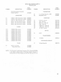
MINI·DISK POWER SUPPLY
PARTS LIST
PART
SYMBOL
DESCRIPTION
NUMBER
DESCRIPTION
SYMBOL
TRANSISTORS
PRINTED CIRCUIT BOARD.
POWER SUPPLY
8190008
01
02
CAPACITORS
Cl
C2
C3
C4
CS
C6
2,200 pF. 25V. Electrolytic, Radial
2,200 pF. 35V, Electrolytic, Rldi.l
ODOl pF. l00V,Polyester, Film
220 J.[F. lev. Electrolytic. Radi.l
220 j,.IF. l6V, Electrolytic, Radi.l
220 JJ.F. 35V. Electrolytic. Radial
CR10
lN5392.
lN5392.
lN5392,
lN5392,
lN4002,
lN4002.
l00V. Silicon
l00V, Silicon
l00V, Silicon
l00V. Silicon
l00V. Silicon
l00V. Silicon
lN5392. l00V. Silicon
1N5392, 100V. Silicon
1N5392, 100V. Silicon
1N5392, 100V. Silicon
Socket, Connector
Plug, Power (4 u)
8050805
8100601
RESISTORS
8328222
8352105
8327221
8327221
8327223
8150392
8150392
8150392
8150392
8150002
8150002
8150392
8150392
8150392
8150392
PLUGS
PI
I.C. Voltage Regulator. 7805
MJE3055. Power
8328223
DIODES
CRt
CR2
CR3
CR4
CRS
CR6
CR7
CR8
CR9
PART
NUM8ER
R1
R2
R3
R4
RS
R6
R7
0.33 ohm,?N. 5"
10K. 1I4W, 5%
560 ohms, 1/4W, 5"
2.2K, 1/4W, 5%
3.300 ohms, 1/4W, 5"
'.500 ohms, 1/4W. 5%
, K, 30%, Variable
8247833
8207210
8207156
8207222
8207233
8207215
8278210
SWITCH
51
OPDT
8489020
TRANSFORMER
TI
117/60Hz
8790012
INTEGRATED CIRCUIT
ZI
Voltage Regulator
8050723
8159008
8159006
NOTE: The 34-eontact Feedthrough Connector (Part Number 85190041
i, not listed or shown" part of the Power Supply. However, it
interconnect' the Power Supply and the Mini·Did( Drive P. C. B.
23
DISK CONTROLLER BOARD
PARTS LIST
SYMBOL
OEseR IPTION
PRINTED CIRCUIT BOARD.
DISK CONTROLLER
PART
NUMBER
CAll
8709094
CAPACITORS
C'
C2
C3
C4
C5
C5
C7
C8
C9
ClO
Cll
C'2
C'3
C'4
C'5
C'6
C17
C'8
C,.
C20
C2,
C22
C23
C24
C25
C26
C27
C26
C29
C30
C31
C32
C33
C34
C35
C36
C37
C38
C39
C40
C4'
j
CR10
CA12
CR13
CR14
CRlS
2.2 p.F. 35V
8395223
CAlB
470pF.50V
68pF,50V
8381474
CRt7
8381684
O.471JF, SOV
0.47 p.F, SOV
0.0 lp.F , SOV
0.47 pF. SOV
0.4 7 p.F. SOV
8384474
CRlB
CAl9
8384474
CR20
8383104
CR2l
4700pF.50V
8382474
8383104
L1
8381274
L2
L3
8381474
8381474
8382124
8394102
8394102
8315472
8383104
8383104
8383104
8383104
8383104
8383104
8150446
8150446
8150446
8150446
8150446
8150446
8150446
8150446
8150446
8150446
8383104
8335683
8383104
8383104
8383104
8335683
8383104
8383104
8383104
8383104
8383104
8315472
8315472
8335683
8335683
8381334
8381334
8150446
8150446
8150446
8150446
I
390 IJh
390 p.h
8419003
680~h
84'0004
8419003
INTEGRATED CIRCUITS
3A
4A
28
38
48
58
2C
3C
'1N4446, Switching
1N4446, Switching
1N4446, Switching
1N4446, Switching
Not Used
24
8150446
INDUCTORS
270 pF. SOV
470pF,50V
470pF,50V
1200pF,50V
0.1 JJF, 20V
0.1 JJF, 20V
4.7 JJF, 20V
0.01/-lF,50V
0.01 JJF, 50V
0.01 JJF, 50V
0.01 JJF, 50V
0.01 JJF, 50V
0.01 JJF, 50V
Not Used
O.OlIJF, 50V
6.81J F,35V
0.Ol1J F,50V
0,01 JJF, 50V
0.01 JJF, 50V
6.8 JJF, 35V
0.01IJF ,50V
0.01 JJF, 50V
0.01 JJF, 50V
0.01 IJF, 50V
0.01 JJF, 50V
4.7 JJF, 20V
4.7 JJF, 20V
6.8 J,lF, 35V
6.8 J,lF, 35V
330 pF, 50V
330 pF, 50V
I
1N4446. Switching
1N4446, Switching
1N4446, Switching
1N4446, Switching
1N4446, Switching
1N4446, Switching
1N4446, Switching
1N4446. Switching
1N4446. Switching
1N4446. Switching
1N4446, Switching
PART
NUMBER
8384474
0.01 p.F, SOV
Not Used
DESCRIPTION
8384474
DIODES
CA'
CA2
CA3
CA4
CA5
SYMBOL
4C
5C
3D
40
50
'E
2E
3E
4E
5E
'F
2F
4F
Me 1733
NE 592A
7406, Buffer and Interface Gate
74LS20, Positive NAND Gate
74LS20, Positive NAND Gate
M LM 311 EL Precision Comp_ator
75463, Dual Peripheral Positive OR
Driver
74LS123, Retriggerable Monostable
Muhivibrator
74LS74, Flip·Flop
74LS74, Flip-Flop
74LS04, Positive NAND Gate
75462, Dual Peripheral Positive
NAND Driver
74LS86, Quadruple 2·input Exclusive
OR Gate
-DIP Shunt, 161>in
74LS14, Schmitt·Trigger Positive
NAND Gate
7407, Buffer and Interface Gate
75462, Dual Peripheral Positive
NAND Driver
74LS221, Dual Monostable Multi·
vibrator w/Sctlmitt-Trigger Inputs
74LS38, 8uffer and Interface Gate
8·resistor Network
74lS38, Buffer and Interface Gate
• If applicable
8050733
8050592
8010406
8020020
8020020
8050311
8050463
8020123
8020074
8020074
8020004
8050462
0020086
8480001
8020014
8010407
8050462
8020221
8020038
8290007
8020038
,
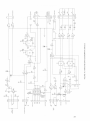
DISK CONTROLLER BOARD
PARTS LIST (Cont'd)
SYMBOL
DESCRIPTION
PART
NUMBER
RESISTORS
8.2 K. 1/4 w, 5%
8,2 K. 1/4 W, 5%
8.2 K. 1/4 W, 5%
27 K, 1/4 W, 5%
27 K, 1/4 W, 5%
3.6 K, 1/4 W, ,,,
Rl
R2
R3
R4
R5
R6
R7
RS
R9
RIO
Rll
R12
R13
R14
R15
R16
R17
R1S
R19
R20
R21
R22
R23
R24
R25
R26
R27
R28
R29
R30
R31
R32
R33
R34
R35
R36
1 K, 1/4 W, 5%
1 K, 1/4W,5%
1 K. 1/4 W, 5%
750 ohms, 1/4 W, 5%
390 ohms, 1/4W.5%
10 K, 1/4 W. 5"
390 ohms, 1J4W.5"
3.09K.1/4W, lor.
768 ohms. 1/4W. '"
3.9 K. 1/4 W, 5%
1 K, 1/4 W. 5"
47K,l/4W,5"
2.2 K, 1/4 W, 5%
2.2 K, 1/4 W. 5%
768 ohms, 1/4W,1%
820ohms. Tl4W, 5%
390 ohms, 1/4 W, 5%
1.54 K, 1/4 W. 1%
768 ohms. 1/4 W. 1%
Not Used
R41
R42
R43
R44
R45
R46
R47
R48
R49
R50
R51
R52
R53
R$4
Not Used
1 K. 1/4W. 5~
1 K. 1/4 W. 5'\
3K.1/4W.5%
10K. 1/4W, 5%
Not Used
1 K.1/4W,5%
300ohms.1/4W.5%
1 K. 1/4 W. 5%
Not Used
Not Used
150ohms,1/4W.5%
1 K. 1/4 W, 5"
13.3 K. 1/4W. 1%
1 K, 1/4 W. 5"
1 K. 1/4 W. 5"
1 K.l/4W.5"(,
1 K, 1/4 W. 5"
1 K. 1/4 W. 5"
8207282
8207282
8207282
8207327
8207321
8207236
8207210
8207210
8207210
8207210
8207210
1 K. 1/4 W, 5"(,
8207210
12K.1I4W.5"
8207212
150 ohms, 1/4 W, 5%
Not Used
8207115
1 K.l/4W,5%
8207210
8207210
8207210
8207210
8207175
8207139
8207310
8207139
8201230
8201176
8207239
8207210
8207347
8207222
8207222
8201176
8207182
8207139
8201215
8201176
SYMBOL
R55
R56
R57
R58
R59
R60
R61
R62
R63
R64
R65
R66
R67
R68
R69
DESCRIPTION
,%
28.7 K, 1/4 W,
Not Used
Not lhed
150 ohms, 2 w. 5%
1 K. 1/4 W, 5%
1 K. 1/4 W. 5%
1 K. 1/4 W, 5%
150 ohms, 1/4 W, 5%
10K,l/4W.5"
1 K.1/4W.5%
750 ohms, 1/4 W. 5%
390 ohms, 1/4 W. 5"
Not Used
1 K, 1/4 W. 5%
1 K. 1/4 W. 5%
PART
NUMBER
8201328
8247115
8207210
8207210
8207210
8207115
8207310
82072lO
8207175
8207139
8207210
8207210
TRANSISTORS
0'
02
03
04
05
06
07
08
2N4124, NPN
2N4124, NPN
2N4124,NPN
2N4124. NPN
2N4125, PNP
Not Used
Not Used
2N4124.NPN
8110124
8110124
8110124
8110124
8100125
8110124
MISCEllANEOUS
16-pin Ie Socket (2)
• 16-pin DIP Shunt Socket
5-pin Right Angle Header
14·pin Right Angle Header (2)
Staking Pin (13)
Resistor. IlJn value - Jumper (2)
4-position PC Mount Housing
S509003
8489001
8519054
8519060
8529014
8200000
8519056
• If Applicable
8207210
8207210
8207230
8207310
8207210
8207130
8207210
8207115
8207210
8201313
25
SERVO IMOTOR CONTROL I BOARD
PARTS LIST
SYMBOL
DESCRIPTION
PART
NUMBER
PART
SYMBOL
PRINTED CIRCUIT BOARD.
SERVO (MOTOR CONTROL)
lp.F,35V
'I-lF,35V
lp.F,35V
1 pF,35V
RESISTORS
8335103
8335103
8335103
8335103
8393474
8394413
0.047 $.IF, 80 V
0.47p.F.35 V
DIODES
CRt
lN4002. Rectifier, Low Power
8150002
R1
R2
R3
R4
R5
R6
R7
R8
R9
RlO
Rll
R12
R13
INDUCTORS
11
3_3 ""h. 1,",
NUMBER
8709096
CAPACITORS
C1
C2
C3
C4
C5
C6
DESCRIPTION
20 K. 1/4 W, 5%
1 M. 1/4 W. 5"
1 K, 1/4 W,5"
1 K, Trim Potentiometer
8207320
8207510
8207210
8289210
1 K.1/4W. 5...
8207210
43.2 K, 1/4 W. '"
470 ohms. 1/4 W. 5%
8201343
8207147
8207147
8207018
8207210
8217001
8217222
8207222
470 ohms. 1/4 W, 5%
18 ohms, 1/4 W, 5%
1 K, 1/4 W, 5%
1 ohm, 1/2W. 5%
2.2 K, 1/4 W, 5"
2.2 K. 1/4 W, 5"
TRANSISTORS
8419005
01
02
TIP110. Power
2N4124.NPN
8110110
8110124
INTEGRATED CIRCUITS
MISCELLANEOUS
U1
LM2917N. Frequ...cv to Voltage
Converter
1Q.pin Ai~t Angle Header
4-40 x 1/4" Screw, Pan Head
4-40 Hex Nut
8050917
DISK DRIVE
PARTS AND SUBASSEMBLIES
SYMBOL
DESCRIPTION
Drive Motor AssemblV
Track "GQ" Switch AssembiV
Write Protect Switch Assembly
Belt Drive
Index Assembly
LED Assembly (Pa"IeIl
Cone Assembly
Latch Assembly
Right H.,d Guide
Left Hand Guide
Front Panel
Front Panel 8ushing
Upper Bearing
Lower Bearing
Module AssembiV SSR
• Stepper Motor Assembly
• Head Carriage Assembly SSR
• Drive Band Stepper
• Included in Module Assembly SSR.
26
8519057
8569032
8579001
DRIVE ASSEMBLY
PARTS LIST
PART
NUMBER
8852015
8852016
8552017
8852018
8552019
8552020
8552021
8552022
8552023
8552024
8552025
8552026
8552027
8552028
8552029
8552030
8552031
8552032
SYMBOL
DESCR IPTION
Drive AssemblV
Disk Controller Board Assembly
Servo Board Assembly
Disk Drive
6·32 x 1/2" Screw, Phillips 121
4-40 x 1/4" Saew 121
;/6 Spacer, Nylon (21
PART
NUMBER
7000009
7000007
7000008
8790104
8569046
8569032
8589025
SECTION V
MINI·OISK SERVICE MANUAL
(MINI 25060 - xx)
INTRODUCTION
This manual provides .!'\Iice information for the Mini-Oisk
Power SJpply. Termination Resistor PKk~e. DIP Shunt,
Jumper Wire and <Able Connectors (for Serial Numberl
MINI2S060 - xxI.
Sel'\lice information for this system can be found in the
SA4QO Minifloppy Diskette Storage Drive Service Manu.I,
published by Shugart Associates, dated March 1977. The
Shugart Manu.t follows these ~.
Rnistor Termination. DIP Shunt lind Jumper (refe, to
2.
The DIP Shunt
~klge
is used in ,II Drives and must
be punched and seated I' iIIustr.ted.
FtguN 151.
The Resistor TermiNltion in the Ie socket is used in
Drive number zero only. It must be removed for Drives
one, two.nd th,....
3.
The Jumper Wire between pins 10 and 32 of Jl is used
on .11 Drives.
...
J ~ W'lI.E aoo£D
TO All OIUVU.
,r.r-",
.
2 0"
~u",. '''CKAGI
e12 'IN 0.' 1IT1 IN UI'
1 "Ulno" TlIIN''''ATION
UN IIOCI(ln fllMC/VI IIt_
CII'T FOfI 011111'1 _1111
l'IlI ' ...lIt 0' ,. fiN 01'
IOCKIT MI)" Il PUNCH
lO .... IItOWN 1"1 ALL
,,~
OIlI\'U.
FIGURE 15. RESISTOR TERMINATION,
DIP SHUNT AND JUMPER.
Fl1lt Ribbon Cabl, A••mblv f. . Figurl 161.
2.
Connector for Drive number one - pins 10, 14 al"ld 32.
Pins must be removed from Drive connectors on the Cable
As5emblv IS follows al"ld as illustrated:
3.
Connector for Drive number two - pins 10. 12.1"1d 32.
4.
Connector for Drive number three - pins 10, 12 and
14.
1.
Connector for Drive number zero - pins 12. 14 and 32.
Do not remove InV pins from the connector to the Expansion Interface.
DAIVE
NUMfIEA ZEAO
DAIVE
NUM8EAON£
DAIVE
NUMBEATWO
DAIVE
NUMBER THAEl
,."
,.
10
10
10
32
32
32
"
"
"
FIGURE 16. CABLE ASSEMBLV - CONNECTOR
PIN REMOVAL CHART.
27
RADIO SHACK
M
A DIVISION OF TANDY CORPORATION
U_S A' FORT WORTH TEXAS 76102
CANADA BARRIE. ONTARIO l4M 4W5
..,....
TANDY CORPORATION
AuSt"'UA
no
'1$ IIICt~ lilOAD
ItTOAlM(iIIf N SW Wi
380
I'dC IfriOuStli1l III N.u. "f(!
n40 /UJo"'N!
"
.ST. IlOolll WlO"!"",
WIST M'Ol.lNClS w<>10 IJIl
PRINTED IN U.S.A.