1
™
All MikroElektronika´s development systems represent irreplaceable tools for
programming and developing microcontroller-based devices. Carefully chosen
components and the use of machines of the last generation for mounting and
testing thereof are the best guarantee of high reliability of our devices. Due to
simple design, a large number of add-on modules and ready to use examples,
all our users, regardless of their experience, have the possibility to develop
WKHLUSURMHFWLQDIDVWDQGHI¿FLHQWZD\
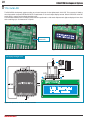
User manual
Development System
BIGdsPIC6
TO OUR VALUED CUSTOMERS
, ZDQW WR H[SUHVV P\ WKDQNV WR \RX IRU EHLQJ LQWHUHVWHG LQ RXU SURGXFWV DQG IRU KDYLQJ FRQ¿GHQFH LQ
mikroElektronika.
The primary aim of our company is to design and produce high quality electronic products and to constantly
improve the performance thereof in order to better suit your needs.
Nebojsa Matic
General Manager
The Microchip name and logo, the Microchip logo, Accuron, dsPIC, KeeLoq, microID, MPLAB, PIC, PICmicro, PICSTART, PRO MATE,
PowerSmart, rfPIC and SmartShunt are registered trademarks of Microchip Technology Incorporated in the U.S.A and other countries.
3
page
BIGdsPIC6 Development System
TABLE OF CONTENTS
Introduction to BIGdsPIC6 Development System ............................................................................. 4
Key Features .................................................................................................................................... 5
1.0. Connecting the System to a PC ................................................................................................ 6
2.0. Supported Microcontrollers ....................................................................................................... 7
3.0. On-board dsPICFlash Programmer ........................................................................................... 9
4.0. ICD Connector .......................................................................................................................... 10
5.0. Power Supply ............................................................................................................................ 11
6.0. A/D Converter Test Inputs ......................................................................................................... 12
7.0. Voltage Reference Source ......................................................................................................... 13
8.0. Serial EEPROM Module ............................................................................................................ 13
9.0. MMC/SD Connector .................................................................................................................. 14
10.0. RS-232 Communication Module ............................................................................................. 15
11.0. CAN Communication Module ................................................................................................. 16
12.0. Real-Time Clock (RTC) ........................................................................................................... 17
13.0. USB UART Module ................................................................................................................. 18
14.0. Piezo Buzzer ........................................................................................................................... 19
15.0. LEDs ...................................................................................................................................... 20
16.0. Push Buttons ........................................................................................................................... 21
17.0. 2x16 LCD ................................................................................................................................ 22
18.0. 128x64 Graphic LCD ............................................................................................................... 23
19.0. Touch Panel ............................................................................................................................ 24
20.0. I/O Ports ..................................................................................................................................25
MikroElektronika
page
4
BIGdsPIC6 Development System
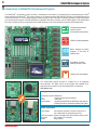
Introduction to BIGdsPIC6 Development System
The BIGdsPIC6™ development system provides a development environment for programming and experimenting with dsPIC®
microcontrollers from Microchip®. The system includes an on-board programmer with mikroICD providing an interface between the
PLFURFRQWUROOHUDQGD3&<RXDUHVLPSO\H[SHFWHGWRZULWHDSURJUDPLQRQHRIWKHGV3,&FRPSLOHUVJHQHUDWHDKH[¿OHDQGSURJUDP
your microcontroller using the on-board GV3,&ÀDVK™ programmer. Numerous modules, such as 128x64 graphic LCD, alphanumeric
2x16 LCD, real-time clock etc, are provided on the board and allow you to easily simulate the operation of the target device.
Full-featured development
system for dsPIC
microcontroller based devices
USB 2.0 on-board programmer
Built-in debugger for testing
programs in real time at
hardware level
A possibility of reading
MMC/SD memory cards
Graphic LCD with backlight
The dsPICFLASH program provides a complete list of all supported
microcontrollers. The latest version of this program with updated list of
supported microcontrollers can be downloaded from our website at
ZZZPLNURHFRP
3DFNDJHFRQWDLQV
Development system: BIGdsPIC6
CD:
product CD with relevant software
Cables:
USB cable
'RFXPHQWDWLRQ
0DQXDOVIRU%,*GV3,&DQGGV3,&ÀDVKTXLFNJXLGHIRU
installing USB drivers, electrical schematic of the system
6\VWHPVSHFL¿FDWLRQ
Power Supply:
over an AC/DC connector (7-23V AC or 9-32V DC); or
over a USB cable for programming (5V DC)
Power consumption:~40mA in idle state when all on-board modules are off
Dimension:
26,5 x 22cm (10,4 x 8,6inch)
Weight:
462g (0.89lbs)
MikroElektronika
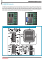
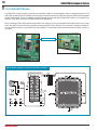
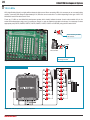
5
1
2
4
3
5
6
7
8
9
page
BIGdsPIC6 Development System
10 11
12
30
29
13
14
28
15
27
16
26
25
24 23
22
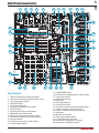
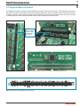
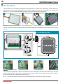
.H\)HDWXUHV
1.
2.
3.
4.
5.
6.
7.
8.
9.
10.
11.
12.
13.
14.
USB 2.0 programmer with mikroICD support
Connector for Microchip’s debugger (ICD2 or ICD3)
CAN communication module
USB UART Module
A/D converter test inputs
Connector A for RS-232 communication
Real-Time Clock
Connector B for RS-232 communication
DIMM-168P socket for MCU cards
Jumper for pull-up/pull-down resistor selection
DIP switches enable pull-up/pull-down resistors
I/O port connectors
DIP switches turn on/off on-board modules
4.096V voltage reference
21
20
19 18
17
15. Serial EEPROM module
16. Potentiometer for adjusting graphic display contrast
17. Touch panel controller
18. Graphic LCD connector
19. Piezo buzzer
20. 3.3V voltage regulator
21. Touch panel connector
22. Push buttons simulate microcontroller digital inputs
23. Jumper for protective resistor shortening
24. Jumper for selecting push buttons’ logic state
25. Reset button
26. MMC/SD card connector
27. Power supply voltage regulator
28. 77 LEDs indicate pins’ logic state
29. Potentiometer for adjusting LCD contrast
30. Alphanumeric LCD display connector
MikroElektronika
page
6
BIGdsPIC6 Development System
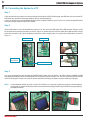
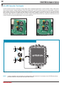
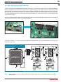
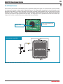
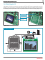
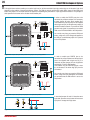
&RQQHFWLQJWKH6\VWHPWRD3&
6WHS
Follow the instructions provided in the relevant manuals and install the dsPICFLASH program and USB driver from the product CD.
USB drivers are essential for the proper operation of the on-board programmer.
In case you already have one of the Mikroelektronika’s dsPIC compilers installed on your PC, there is no need to reinstall USB drivers
as they are already installed along with the compiler.
6WHS
Use the USB cable to connect the development system to a PC. One end of the USB cable, with a USB connector of B type, should
be connected to the development system, as shown in Figure 1-2, whereas the other end of the cable with a USB connector of A type
should be connected to a PC. When establishing a connection, make sure that jumper J11 is placed in the USB position as shown in
Figure 1-1.
AC/DC connector
USB connector
1
2
J11 power
supply selector
POWER SUPPLY switch
)LJXUHPower supply
)LJXUH: Connecting USB cable
6WHS
Turn on your development system by setting the POWER SUPPLY switch to the ON position. Two LEDs marked as POWER and USB
LINK will be automatically turned on indicating that your development system is ready to use. Use the on-board programmer and the
dsPICFLASH program to dump a hex code into the microcontroller and employ the system to test and develop your projects.
127(
If some additional modules are used, such as LCD, GLCD etc, it is necessary to place them properly on the development
V\VWHPZKLOHLWLVWXUQHGRII2WKHUZLVHHLWKHUFDQEHSHUPDQHQWO\GDPDJHG5HIHUWR¿JXUHEHORZIRUWKHSURSHUSODFLQJRI
the additional modules.
)LJXUHPlacing additional modules on the board
MikroElektronika
7
page
BIGdsPIC6 Development System
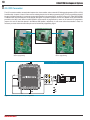
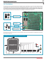
2.0. Supported Microcontrollers
The BIGdsPIC6 development system provides a DIMM-168P connector to place an MCU card into. This development system comes
with an MCU card with a microcontroller in 80-pin TQFP package soldered on it, Figure 2-3. Besides, the MCU card alone provides an
oscillator as well as 80 soldering pads connected to the microcontroller pins. Each pad is marked the same as the pin it is connected
to. Soldering pads also make connection between the MCU card and target device’s modules easy.
DIMM-168P
connector for placing
the MCU card with
a microcontroller in
TQFP package
)LJXUHDIMM-168P connector with the MCU card inserted
)LJXUHDIMM-168P connector
)LJXUHMCU card with an 80-pin microcontroller in TQFP package soldered on it
)LJXUHSchematic of the DIMM-168P connector’s pinout
MikroElektronika
page
8
BIGdsPIC6 Development System
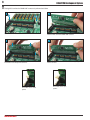
Placing MCU card into the DIMM-168P connector is performed as follows:
1
A
2
B
Open extraction levers A and B
Place the MCU card into the DIMM-168P connector
4
3
Push the MCU card down gently into the DIMM-168P connector and
lift extraction levers slowly at the same time
Extraction levers used to
¿[WKH0&8FDUGLQµFORVHG
position
MikroElektronika
Close the extraction levers when the MCU card is properly placed
into the connector
Extraction levers used to
¿[WKH0&8FDUGLQµRSHQ
position
9
page
BIGdsPIC6 Development System
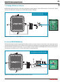
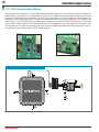
2QERDUGGV3,&)ODVK3URJUDPPHU
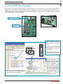
A programmer is a necessary tool when working with microcontrollers. It is used to load a hex code into the microcontroller and
provides an interface between the microcontroller and a PC. The BIGdsPIC6 features an on-board GV3,&)ODVK programmer. The
dsPICFLASH SURJUDP LV XVHG IRU ORDGLQJ D KH[ ¿OH LQWR WKH PLFURFRQWUROOHU )LJXUH VKRZV FRQQHFWLRQ EHWZHHQ WKH FRPSLOHU
dsPICFLASH program and the microcontroller.
Programmer’s USB connector
Programmer’s chip
)LJXUH: USB connector’s front side
)LJXUHOn-board programmer
1 Write a program in one of the
dsPIC compiler and generate a
KH[¿OH
Compiling program
2 Use the dsPICFLASH program
to select desired microcontroller to
be programmed;
3
3 Click the Write button to dump
the code into the microcontroller.
hex code loading
1
2
Write a code in one of the dsPIC compilers, generate
DKH[¿OHDQGHPSOR\WKHRQERDUGSURJUDPPHU
to load the code into the microcontroller.
On the left side of the
dsPICFLASH program’s main
window, there is a number of
options for setting the operation
of the microcontroller to be
used. A number of options
which enable the programming
process are provided on the right
side of the window. Positioned
in the bottom right corner of
the window, the Progress bar
enables you to monitor the
programming progress.
)LJXUHProgramming process
MikroElektronika
page
10
BIGdsPIC6 Development System
,&'&RQQHFWRU
The ICD connector enables communication between the microcontroller and an external ICD debugger/programmer (ICD2 or ICD3)
from Microchip. Jumpers J14 and J15 are used for selecting the pin to be fed with programming signal. For the programming signal to
be sent to the microcontroller, it is necessary to place both jumpers in the same position, as shown in Figure 4-3. Either RB0 and RB1
or RB6 and RB7 microcontroller pins can be fed with this signal. The position of jumpers J14 and J15 depends on the microcontroller
provided on the MCU card. When the dsPIC30F6014 microcontroller is programmed by means of the external ICD programmer,
jumpers J14 and J15 should be placed in the RB0 and RB1 position, respectively. In case some other microcontroller is used, it is
necessary to check which microcontroller pins can be fed with the programming signal.
)LJXUH: Pins RB6 and RB7 are
used for programming
)LJXUH: Pins RB0 i RB1 are
used for programming
([WHUQDO,&'SURJUDPPHUFRQQHFWHGWR5%DQG5%SLQV
)LJXUHICD connector’s pinout and pin designations
MikroElektronika
11
page
BIGdsPIC6 Development System
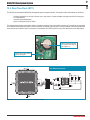
5.0. Power supply
The BIGdsPIC6 development system may use one of two power supply sources:
1. +5V PC power supply through the USB programming cable; and
2. External power supply source connected to an AC/DC connector provided on the development board.
7KH0&$YROWDJHUHJXODWRUDQG*UHW]UHFWL¿HUDUHXVHGWRHQDEOHH[WHUQDOSRZHUVXSSO\YROWDJHWREHHLWKHU$&LQWKHUDQJHRI
7V to 23V) or DC (in the range of 9V to 32V). Jumper J11 is used as a power supply source selector. To make advantage of the USB
power supply, jumper J11 should be placed in the USB position. When using the external power supply, jumper J11 should be placed
in the EXT position. The development system is turned on/off by switching the position of the POWER SUPPLY switch.
AC/DC connector
Power supply
voltage regulator
USB connector
POWER SUPPLY signal LED
Jumper J11 as
a power supply
source selector
POWER SUPPLY switch
)LJXUH: Power supply
Powering over an
AC/DC connector
Powering over a
USB connector
)LJXUH: Power supply source schematic
MikroElektronika
page
12
BIGdsPIC6 Development System
6.0. A/D Converter Test Inputs
An A/D converter is used for converting an analog voltage into the appropriate digital value. The A/D converter is linear, which means
that converted number is linearly dependent on the input voltage value. The A/D converter built into the microcontroller converts an
analog voltage value into a 10-bit number. Potentiometers P3 and P4 enable voltage to vary between 0 and 5V. The microcontroller
with a built-in A/D converter is supplied with this voltage via test inputs. Jumpers J16 and J17 are used for selecting one of the
following pins RB8 - RB15 to be supplied with A/D conversion voltage. Resistors R28 and R29 have a protective function and are used
WROLPLWFXUUHQWÀRZWKURXJKWKHSRWHQWLRPHWHURUWKHPLFURFRQWUROOHUSLQ
)LJXUH: ADC (jumpers in default position)
)LJXUH: Pins RB8 and RB12 used as
input pins for A/D conversion
$'FRQYHUVLRQLVSHUIRUPHGYLD5%DQG5%PLFURFRQWUROOHUSLQV
)LJXUH: A/D converter test inputs and microcontroller connection schematic
127(
In order to enable the microcontroller to accurately perform A/D conversion, it is necessary to turn off LEDs and pull-up/
pull-down resistors on the port pins used by the A/D converter.
MikroElektronika
13
page
BIGdsPIC6 Development System
9RWDJH5HIHUHQFH6RXUFH
BIGdsPIC6 provides the MCP1541 circuit which generates the voltage reference used for A/D conversion. The value of the voltage
reference is 4.096V and it is brought to the microcontroller via RA10 or RB0 pin.
0LFURFRQWUROOHULVIHGZLWKYROWDJH
UHIHUHQFHYLDWKH5$SLQ
)LJXUH: Voltage reference connection schematic
6HULDO((35200RGXOH
EEPROM (Electrically Erasable Programmable Read-Only Memory) is a built-in memory module used to store data that should be
saved when the power supply goes off. The 24AA01 circuit can store up to 1Kbit data and communicates with the microcontroller through
pins RG2 and RG3 using I2C communication. In order to enable connection between the EEPROM module and the microcontroller, it
is necessay to set switches 3 and 4 on the DIP switch SW12 to the ON the position.
6HULDO((3520LVFRQQHFWHGWRWKH
PLFURFRQWUROOHUYLDSLQV5*DQG5*
)LJXUH: Serial EEPROM module and microcontroller connection schematic
MikroElektronika
page
14
BIGdsPIC6 Development System
9.0. MMC/SD Connector
The MMC/SD connector enables the memory card to be interfaced to the microcontroller in order to expand microcontroller memory.
To enable serial communication between the microcontroller and the memory card it is necessary to adjust their voltage levels.
Memory card is powered with the 3.3V power supply voltage (VCC-MMC) generated by the REG1 voltage regulator, whereas the
value of the microcontroller power suplly voltage is 5V (VCC). A bus transceiver 74LVCC3245 is used here to adjust these voltage
levels. In addition, in order to establish communication between memory card and microcontroller, it is necessary to set switches 6, 7
and 8 on the DIP switch SW12 as well as switches 1 and 2 on the DIP switch SW13 to the ON position.
)LJXUH: MMC/SD connector
)LJXUH: MMC/SD memory card
00&6'FDUGFRPPXQLFDWHVWRWKHPLFURFRQWUROOHUYLD0,62026,6&.00&&6DQG00&&'OLQHV
)LJXUH: MMC/SD connector and microcontroller connection schematic
MikroElektronika
15
page
BIGdsPIC6 Development System
56&RPPXQLFDWLRQ0RGXOH
USART (8QLYHUVDO6\QFKURQRXV$V\QFKURQRXV5HFHLYHU7UDQVPLWWHU) is one of the most common ways of exchanging data between
the PC and peripheral units. RS-232 serial communication is performed through a 9-pin SUB-D connector and the microcontroller
USART module. The BIGdsPIC6 provides two RS-232 ports, RS-232A and RS-232B. Use switches RX232-A and TX232-A on the DIP
switch SW14 to enable port RS-232A. Likewise, use switches RX232-B and TX232-B on the DIP switch SW14 to enable port RS-232B.
The microcontroller pins used in such communication are marked as follows: RX - UHFHLYHGDWDOLQH and TX -WUDQVPLWGDWDOLQH. Data
rate goes up to 115 kbps.
In order to enable the USART module of the microcontroller to receive input signals with different voltage levels, it is necessary to
adjust these levels using an IC circuit such as MAX202 (MAX232).
RS-232 connector
)LJXUH: RS-232 module
The function of switches 1, 2, 3 and 4 on the DIP switch SW14 is to determine which of the microcontroller pins are to be used as RX
and TX lines, Figure 10-2.
3RUWV56$DQG56%DUHFRQQHFWHG
WRWKHPLFURFRQWUROOHU
)LJXUH: RS-232 module connection schematic
127(
Make sure that your microcontroller is provided with the USART module as it is not necessarily integrated in all dsPIC
microcontrollers.
MikroElektronika
page
16
BIGdsPIC6 Development System
11.0. &$1&RPPXQLFDWLRQ0RGXOH
CAN (Controller Area Network) is a communication standard primarily intended for use in automotive industry. It enables the
microcontroller to communicate to a car device without using a host PC. In addition, such communication is widely used in industrial
automation. The BIGdsPIC6 uses the MCP2551 circuit for CAN communication. This circuit provides an interface between the
microcontroller and some peripheral device. To enable connection between the microcontroller and MCP2551, it is necessary to set
switches 5 and 7 on the DIP switch SW14 to the ON position. Switches 6 and 8 on the DIP switch SW14 may also be used for this
purpose. Which of these switches is to be used depends solely on the arrangement of the microcontroller pins connected to CAN
communication lines. The RX line is connected to the microcontroller via RG0 and RF0 microcontroller pins, whereas the TX line is
connected to the microcontroller via RG1 and RF1 microcontroller pins.
)LJXUH: CAN module connector
)LJXUH: CAN module
&$1FRPPXQLFDWLRQLVHQDEOHGYLD',3VZLWFK6:
)LJXUH: Microcontroller and MCP2551 connection schematic
MikroElektronika
17
page
BIGdsPIC6 Development System
5HDO7LPH&ORFN57&
The DS1307 circuit enables the BIGdsPIC6 development system to keep the real time. The real-time clock’s main features are as follows:
- providing information on seconds, minutes, hours, days, days in a week and dates including corrections for a leap year
- I2C serial interface
- automatic power-fail detection
- power consumption less than 500nA
The real-time clock is widely used in alarm devices, industrial controllers, mass-consumption products etc. The real-time clock provided
on the BIGdsPIC6 development system is used to generate an interrupt at pre-set time. In order to establish connection between the
microcontroller and real-time clock it is necessary to set switches RG3, RG2 and RA15 on the DIP switch SW12 to the ON position.
3V battery enables the operation
of the real-time clock when the
power supply is off
Quartz-crystal provides real-time
clock with clock signal
)LJXUH: Real-time clock
5HDOWLPHFORFNLVFRQQHFWHGWRWKHPLFURFRQWUROOHUYLD
5*5*DQG5$SLQV
)LJXUH: Real-time clock and microcontroller connection schematic
MikroElektronika
page
18
BIGdsPIC6 Development System
86%8$570RGXOH
The USB UART module is used to connect the microcontroller provided on the development system to external USB devices. The
USB UART module features the FT232RL circuit providing an interface between the USB device and serial UART module integrated
into the microcontroller. In order to establish connection between the microcontroller and USB UART module, it is necessary to set
switches 1 (RF2) and 2 (RF3) on the DIP switch SW12 to the ON position.
When connecting a UART device and the microcontroller, it is necessary to cross connect data send and data receive lines. In other
words, the UART’s RX pin should be connected to the microcontroller’s TX pin, while the TX pin should be connected to the RX pin.
It is not possible to directly connect UART’s and microcontroller’s TX lines since the microcontroller wouldn’t be able to receive nor
send data.
USB connector of B type
)LJXUH: USB UART module
86%FRQQHFWRURI%W\SHLVFRQQHFWHGWRWKHPLFURFRQWUROOHU
)LJXUH: USB connector and microcontroller connection schematic
MikroElektronika
19
page
BIGdsPIC6 Development System
3LH]R%X]]HU
Due to a built-in piezo buzzer, the develompent system is capable of emitting audio signals. For the piezo buzzer to operate normally
LW LV QHFHVVDU\ WR JHQHUDWH D YROWDJH VLJQDO RI VSHFL¿HG IUHTXHQF\ 7KH YROWDJH VLJQDO LV JHQHUDWHG LQ WKH PLFURFRQWUROOHU E\ WKH
appropriate code written to its memory. Remember, when writing the voltage signal generation code, the piezo buzzer’s resonant
IUHTXHQF\LVN+],QDGGLWLRQRWKHUIUHTXHQFLHVLQWKHUDQJHEHWZHHQ+]DQGN+]FDQEHXVHGEXWWKHEHVWSHUIRUPDQFH
LVSURYLGHGE\IUHTXHQFLHVUDQJLQJEHWZHHQN+]DQGN+]7KHYROWDJHVLJQDOFDQEHJHQHUDWHGYLDWKH5'PLFURFRQWUROOHUSLQ
Jumper J18 is used to connect the piezo buzzer with the RD8 microcontroller pin.
Transistor Q5 is used to amplify
voltage signal generated by the
microcontroller
Piezo buzzer’s resonant
IUHTXHQF\N+]
)LJXUH: Piezo Buzzer
3LH]REX]]HULVFRQQHFWHGWRWKH
PLFURFRQWUROOHUYLDSLQ5'
)LJXUH: Piezo buzzer and microcontroller connection schematic
MikroElektronika
page
20
BIGdsPIC6 Development System
15.0. LEDs
/('/LJKW(PLWWLQJ'LRGHLVDKLJKO\HI¿FLHQWHOHFWURQLFOLJKWVRXUFH:KHQFRQQHFWLQJ/('VLWLVQHFHVVDU\WRXVHDFXUUHQWOLPLWLQJ
resistor. A common LED voltage is approximately 2.5V, while the current varies from 1 to 20mA depending on the type of LED. The
BIGdsPIC6 uses LEDs with current I=1mA.
There are 77 LEDs on the BIGdsPIC6 development system which visually indicate the state of each microcontroller I/O pin. An
active LED indicates that a logic one (1) is present on the pin. In order to enable the pin state to be shown, it is necessary to select
appropriate port (PORTA, PORTB, PORTC, PORTD, PORTE, PORTF, PORTG or PORTG/E) using the DIP switch SW11.
Notch indicating the SMD
LED cathode
Microcontroller
SMD resistor limiting current
ÀRZWKURXJKDQ/('
)LJXUH: LEDs
3RUW3257%/('VDUHWXUQHGRQ
)LJXUH: LEDs and port PORTB connection schematic
MikroElektronika
21
page
BIGdsPIC6 Development System
16.0. 3XVK%XWWRQV
The logic state of all microcontroller input pins may be changed by means of push buttons. Jumper J13 is used to determine the logic
state to be applied to the desired microcontroller pin by pressing appropriate push button. The function of the protective resistor is to limit
the maximum current, thus preventing the development system and peripheral modules from being damaged in case a short circuit occurs. If needed, advanced users may shorten such resistor using jumper J12. Right next to the push buttons, there is a RESET button
which is not directly connected to the microcontroller pin. The reset signal is generated by the programmer.
Push buttons used for
simulating digital inputs
Jumper J12 used to shorten
protective resistor
RESET button
Jumper J13 used for selecting
logic state to be applied to the
pin by pressing push button
)LJXUH: Push buttons
By pressing any push button when jumper J13 is in the VCC position, a logic one (5V) will be applied to the appropriate microcontroller
pin, as shown in Figure 16-2.
%\SUHVVLQJDSXVKEXWWRQWKHDSSURSULDWHSLQZLOOEHGULYHQKLJK
)LJXUH: Push buttons and port PORTB connection schematic
MikroElektronika
page
22
BIGdsPIC6 Development System
17.0. 2x16 LCD
The BIGdsPIC6 development system provides an on-board connector for the alphanumeric 2x16 LCD. This connector is linked to
the microcontroller via ports PORTB and PORTD. Potentiometer P1 is used to adjust display contrast. Switch LCD-GLCD on the DIP
switch SW11 is used to turn the display backlight on/off.
Communication between the LCD and the microcontroller is performed in a 4-bit mode. Alphanumeric digits are displayed in two lines
each containing up to 16 characters of 7x5 pixels.
Contrast adjustment
potentiometer
)LJXUH. Alphanumeric LCD connector
/&'GLVSOD\EDFNOLJKWLVRQ
)LJXUHAlphanumeric 2x16 LCD connection schematic
MikroElektronika
)LJXUH: Alphanumeric 2x16 LCD
23
page
BIGdsPIC6 Development System
[*UDSKLF/&'
128x64 graphic LCD (GLCD) is connected to the microcontroller via PORTB and PORTD ports and enables graphic content to be
displayed. It has the screen resolution of 128x64 pixels, which allows diagrams, tables and other graphic content to be displayed.
As both ports are also used for the operation of 2x16 LCD, the displays cannot be used simultaneously. Potentiometer P2 is used for
the GLCD display contrast adjustment. Switch 8 (LCD-GLCD) on the DIP switch SW11 is used to turn the display backlight on/off.
GLCD display connector
Touch panel connector
Contrast adjustment
potentiometer
)LJXUH: GLCD
)LJXUH: GLCD connector
*/&'GLVSOD\EDFNOLJKWLVRQ
)LJXUH: GLCD connection schematic
MikroElektronika
page
24
BIGdsPIC6 Development System
7RXFK3DQHO
The touch panel is a thin, self-adhesive, transparent, touch-sensitive panel. It is placed over a GLCD display. Its main function is to
UHJLVWHUSUHVVXUHDWVRPHVSHFL¿FGLVSOD\SRLQWDQGWRIRUZDUGLWVFRRUGLQDWHVLQWKHIRUPRIDQDORJYROWDJHWRWKHPLFURFRQWUROOHU
Switches 5, 6, 7 and 8 on the DIP switch SW13 are used to connect the microcontroller and touch panel.
1
3
4
)LJXUH: Placing touch panel over a GLCD
)LJXUHVKRZVKRZWRSODFHDWRXFKSDQHORYHUD*/&'GLVSOD\0DNHVXUHWKDWWKHÀDWFDEOHLVWRWKHOHIWRIWKH*/&'DVVKRZQ
in Figure 4.
7RXFKSDQHOLVFRQQHFWHGWRWKHPLFURFRQWUROOHU
YLDSLQV5%5%5)DQG5)
)LJXUH: Touch panel connection schematic
1
3
4
: Connecting touch panel
)LJXUHVKRZVLQGHWDLOKRZWRFRQQHFWDWRXFKSDQHOWRWKHPLFURFRQWUROOHU%ULQJWKHHQGRIWKHÀDWFDEOHFORVHWRWKH&1
FRQQHFWRU)LJXUH3OXJWKHFDEOHLQWRWKHFRQQHFWRU)LJXUHDQGSUHVVLWHDVLO\VRDVWRIXOO\¿WWKHFRQQHFWRU)LJXUH1RZD
GLCD can be plugged into the appropriate connector (Figure 4).
127(
LEDs and pull-up/pull-down resistors on ports PORTB and PORTF must be off when using a touch panel.
MikroElektronika
25
page
BIGdsPIC6 Development System
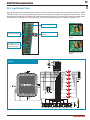
20.0. Input/Output Ports
Along the right side of the development system, there are ten 10-pin connectors connected to the microcontroller’s I/O ports. Pins RB0,
RB1, RB6 and RB7 are used for programming and therefore are not directly connected to the appropriate 10-pin connector, but via
the programmer’s multiplexer. DIP switches SW1-SW10 enable each connector pin to be connected to one pull-up/pull-down resistor.
Whether pins of some port are to be connected to a pull-up or a pull-down resistor depends on the position of jumpers J1-J10.
PORTA 2x5 male connector
Jumper for pull-up/pulldown resistor selection
Additional module connected
to PORTC
)LJXUH J9 in pull-down
position
DIP switch to turn on
pull-up/pull-down resistors for each port pin
)LJXUH: I/O ports
)LJXUH J9 in pull-up
position
3RUW3257%SLQVDUHFRQQHFWHGWRSXOOGRZQ
resistors
)LJXUH: Port PORTB connection schematic
MikroElektronika
page
26
BIGdsPIC6 Development System
Pull-up/pull-down resistors enable you to set the logic level on all microcontroller’s input pins when they are in idle state. Such level
depends on the position of the pull-up/pull-down jumper. The RD8 pin with the relevant DIP switch SW6, jumper J6 and RD8 push
button with jumper J13 are used here for the purpose of explaining the performance of pull-up/pull-down resistors. The principle of
their operation is the same as for all other microcontroller pins.
In order to enable the PORTD port pins to be
connected to pull-down resistors, it is necessary
to place jumper J6 in the Down SRVLWLRQ ¿UVW
This enables any PORTD port pin to be supplied
with a logic zero (0V) in idle state over jumper J6
and 8x10k resistor network. To provide the RD8
pin with such signal, it is necessary to set switch
RD8 on the DIP switch SW6 to the ON position.
As a result, every time you press the RD8 push
button, a logic one (VCC voltage) will appear on
the RD8 pin, provided that jumper J13 is placed
in the VCC position.
)LJXUH: Jumper J6 in pull-down position and jumper J13 in pull-up position
In order to enable port PORTD pins to be
connected to pull-up resistors and the port input
pins to be supplied with a logic zero (0), it is
necessary to place jumper J6 in the Up position
and jumper J13 in the GND position.
This enables any port PORTD input pin, when
it is in idle state, to be driven high (5V) over the
10k resistor.
As a result, every time you press the RD8 push
button, a logic zero (0V) will appear on the RD8
pin, provided that the RD8 switch is set to the
ON position.
)LJXUH Jumper J6 in pull-up and jumper J13 in pull-down position
In case that jumpers J6 and J13 have the same
logic state, pressure on any button will not cause
input pins to change their logic state.
)LJXUH Jumpers J6 and J13 in the same positions
MikroElektronika
DISCLAIMER
All the products owned by MikroElektronika are protected by copyright law and international copyright treaty.
Therefore, this manual is to be treated as any other copyright material. No part of this manual, including
product and software described herein, may be reproduced, stored in a retrieval system, translated or
transmitted in any form or by any means, without the prior written permission of MikroElektronika. The
PDQXDO3')HGLWLRQFDQEHSULQWHGIRUSULYDWHRUORFDOXVHEXWQRWIRUGLVWULEXWLRQ$Q\PRGL¿FDWLRQRIWKLV
manual is prohibited.
MikroElektronika provides this manual ‘as is’ without warranty of any kind, either expressed or implied,
LQFOXGLQJEXWQRWOLPLWHGWRWKHLPSOLHGZDUUDQWLHVRUFRQGLWLRQVRIPHUFKDQWDELOLW\RU¿WQHVVIRUDSDUWLFXODU
purpose.
MikroElektronika shall assume no responsibility or liability for any errors, omissions and inaccuracies that may
DSSHDULQWKLVPDQXDO,QQRHYHQWVKDOO0LNUR(OHNWURQLNDLWVGLUHFWRUVRI¿FHUVHPSOR\HHVRUGLVWULEXWRUVEH
OLDEOHIRUDQ\LQGLUHFWVSHFL¿FLQFLGHQWDORUFRQVHTXHQWLDOGDPDJHVLQFOXGLQJGDPDJHVIRUORVVRIEXVLQHVV
SUR¿WVDQGEXVLQHVVLQIRUPDWLRQEXVLQHVVLQWHUUXSWLRQRUDQ\RWKHUSHFXQLDU\ORVVDULVLQJRXWRIWKHXVH
of this manual or product, even if MikroElektronika has been advised of the possibility of such damages.
MikroElektronika reserves the right to change information contained in this manual at any time without prior
notice, if necessary.
HIGH RISK ACTIVITIES
The products of MikroElektronika are not fault – tolerant nor designed, manufactured or intended for use or
resale as on – line control equipment in hazardous environments requiring fail – safe performance, such as
LQWKHRSHUDWLRQRIQXFOHDUIDFLOLWLHVDLUFUDIWQDYLJDWLRQRUFRPPXQLFDWLRQV\VWHPVDLUWUDI¿FFRQWUROGLUHFW
life support machines or weapons systems in which the failure of Software could lead directly to death,
SHUVRQDOLQMXU\RUVHYHUHSK\VLFDORUHQYLURQPHQWDOGDPDJHµ+LJK5LVN$FWLYLWLHV¶0LNUR(OHNWURQLNDDQGLWV
VXSSOLHUVVSHFL¿FDOO\GLVFODLPDQ\H[SUHVVHGRULPSOLHGZDUUDQW\RI¿WQHVVIRU+LJK5LVN$FWLYLWLHV
TRADEMARKS
The Mikroelektronika name and logo, the Mikroelektronika logo, mikroC, mikroC PRO, mikroBasic, mikro%DVLF352PLNUR3DVFDOPLNUR3DVFDO352$95ÀDVK3,&ÀDVKGV3,&SURJ)-SURJ362&SURJ$95SURJSURJ$50ÀDVK(DV\3,&(DV\3,&%LJ3,&%LJ3,&GV3,&352(DV\%(DV\$50
(DV\$95(DV\$95%LJ$95(DV\GV3,&$(DV\36R&(DV\956WDPS/9)-/9$/90;
3,&0;0XOWL0HGLD%RDUG3,&3/&3,&3/&3,&3/&6PDUW*60*35681,'6DUHWUDGHPDUNV
of Mikroelektronika. All other trademarks mentioned herein are property of their respective companies.
All other product and corporate names appearing in this manual may or may not be registered trademarks
RUFRS\ULJKWVRIWKHLUUHVSHFWLYHFRPSDQLHVDQGDUHRQO\XVHGIRULGHQWL¿FDWLRQRUH[SODQDWLRQDQGWRWKH
RZQHUV¶EHQH¿WZLWKQRLQWHQWWRLQIULQJH
©MikroelektronikaTM$OO5LJKWV5HVHUYHG
,I\RXKDYHDQ\TXHVWLRQVFRPPHQWVRUEXVLQHVVSURSRVDOVGRQRWKHVLWDWHWRFRQWDFWXVDWRI¿FH#PLNURHFRP
If you are experiencing some problems with any of our products or just need additional information, please place your ticket at
www.mikroe.com/en/support
If you want to learn more about our products, please visit our website at www.mikroe.com
Mouser Electronics
Authorized Distributor
Click to View Pricing, Inventory, Delivery & Lifecycle Information:
mikroElektronika:
MIKROE-504