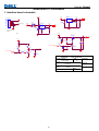
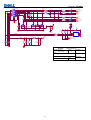
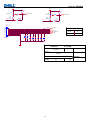
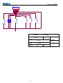
1
Service Manual
Service Manual
LCD Monitor E1709W
-0-
1
Service Manual Versions and Revision
No.
Version
Release Date
Revision
1
1.0
2008/08/25
Initial Release
Copyright
Copyright 2007 InnoLux Display. Corp. Ltd
All Rights Reserved
This manual may not, in whole or in part, be copied, Photocopied, reproduced, translated, or converted to any
electronic or machine readable form without prior written permission of Foxconn Tech. Corp. Ltd.
Dell E1709W Service Manual
Service Manual
Table of Contents
CHAPTER 1- PRECAUTIONS & SAFETY NOTICES .............................................................................................................................. 3
1.
2.
3.
SAFETY PRECAUTIONS ........................................................................................................................................................ 3
PRODUCT SAFETY NOTICE .................................................................................................................................................. 3
SERVICE NOTES .................................................................................................................................................................... 3
CHAPTER 2- SERVICE TOOLS & EQUIPMENT REQUIRED ................................................................................................................. 4
CHAPTER 3- CIRCUIT THEORY.............................................................................................................................................................. 5
1.
2.
3.
4.
5.
6.
7.
8.
BLOCK DIAGRAM ....................................................................................................................................................................... 5
ELECTRONIC CIRCUIT THEORY ................................................................................................................................................... 7
FACTORY PRESET TIMING TABLE..................................................................................................................................... 13
POWER ON/OFF SEQUENCY..................................................................................................................................................... 13
D-SUB CONNECTOR PIN ASSIGNMENT ..................................................................................................................................... 14
AC OUTLET PIN ASSIGNMENT .................................................................................................................................................. 14
INNER CONNECTOR PIN ASSIGNMENT ........................................................................................................................................ 14
KEY PARTS PIN ASSIGNMENTS.................................................................................................................................................. 16
CHAPTER 4- DISASSEMBLY & ASSEMBLY ........................................................................................................................................ 21
1.
2.
3.
EXPLODED DIAGRAM ............................................................................................................................................................... 21
E1709WFPF DISASSEMBLY BLOCK .......................................................................................................................................... 22
ASSEMBLY BLOCK ................................................................................................................................................................... 23
CHAPTER 5- TEST AND ADJUSTMENT............................................................................................................................................... 24
1.
2.
3.
4.
5.
6.
7.
FUNCTION KEY DEFINITIONS ..................................................................................................................................................... 24
OSD CONTROL....................................................................................................................................................................... 24
FACTORY MODE INTRODUCTION ................................................................................................................................................ 26
BURN-IN PATTERN.................................................................................................................................................................... 27
AUTO COLOR BALANCE (AUTOMATICALLY CALIBRATE CHIP ADC PARAMETER BY USING CHIP INTERNAL DAC.)................................... 27
UPLOAD FIRMWARE TO MCU VIA VGA CABLE ............................................................................................................................ 26
AFTER REPAIR, TO ENSURE THE QUALITY YOU SHOULD DO THE FOLLOWING TEST AND ADJUSTMENT. .................................................. 27
CHAPTER 6- TROUBLE SHOOTING..................................................................................................................................................... 30
1.
2.
3.
4.
5.
6.
COMMON ACKNOWLEDGE......................................................................................................................................................... 30
NO POWER LED OFF .............................................................................................................................................................. 30
POWER NORMAL LED AMBER ................................................................................................................................................... 31
BACKLIGHT CAN’T BE TURNED ON .............................................................................................................................................. 32
NO PICTURE BACKLIGHT ON.................................................................................................................................................... 33
AT 32-GRAY SCALE PATTERN, COLOR LOST IN SOME SCALE ........................................................................................................... 34
CHAPTER 7- RECOMMENDED PART LIST .......................................................................................................................................... 35
ATTACHMENT 1- BILL OF MATERIAL .................................................................................................................................................. 37
ATTACHMENT 2- SCHEMATIC.............................................................................................................................................................. 47
ATTACHMENT 3- PCB LAYOUT ............................................................................................................................................................ 52
2
Service Manual
Chapter 1- PRECAUTIONS & SAFETY NOTICES
SAFETY PRECAUTIONS
This monitor is manufactured and tested on a ground principle that a user’s safety comes first.
However, improper used or installation may cause damage to the monitor as well as to the
user.
WARNINGS:
This monitor should be operated only at the correct power sources indicated on the rating
label on the rear cover of the monitor. If you’re unsure the power supply in your residence,
consult your local dealer or Power Company.
Use only the specified power cord that comes with this monitor.
Do not try to repair the monitor by yourself, as it contains no user-serviceable parts. This
monitor should only be repaired by a qualified technician.
Do not remove the monitor cabinet. There is high-voltage parts inside that may cause
electric shock to human bodies.
Stop using the monitor if the cabinet is damaged. Have it checked by a service technician.
Put your monitor only in a lean, cool, dry environment. If it gets wet, unplug the power
cable immediately and consult your closed dealer.
Always unplug the monitor before cleaning it. Clean the cabinet with a clean, dry cloth.
Apply non-ammonia based cleaner onto the cloth, not directly onto the class screen.
Do not place heavy objects on the monitor or power cord.
z
z
z
z
z
z
z
z
PRODUCT SAFETY NOTICE
Many electrical and mechanical parts in this chassis have special safety visual inspections
and the protection afforded by them cannot necessarily be obtained by using replacement
components rated for higher voltage, wattage, etc. Before replacing any of these components
read the parts list in this manual carefully. The use of substitute replacement parts, which do
not have the same safety characteristics as specified in the parts list, may create shock, fire,
or other hazards.
SERVICE NOTES
z
When replacing parts on circuit boards, clamp the solder wires around terminals before
soldering.
z
Keep wires away from high voltage, high temperature components and sharp edges.
z
Keep wires in their original position so as to reduce interference.
z
Adjustment of this product please refers to the user’ manual.
z
Use Pb free solder wire for circuit board preparation.
3
Service Manual
Chapter 2- SERVICE TOOLS & EQUIPMENT REQUIRED
1.
2.
3.
4.
5.
6.
7.
8.
9.
SIGNAL GENERATOR
MULTIMETER
SCREW DRIVER
OSCILLOSCOPE
Soldering IRON
SOLDER (Lead free, RoHS compliance)
Color Analyzer
Fox_VISP_Programmer
Fox_VEDID_Programmer
4
Service Manual
Chapter 3- CIRCUIT THEORY
Block Diagram
There are 2pcs PCBA in this monitor, one is power& inverter board which is a single layer board,
and one is interface board&keypad which is OSD control. The system function block diagram as
below
This PWA is included switching power supplier, inverter for CCFL and interface board.(fig.1)
ON/OFF Control
+5V DC
1
+5V DC
To
Lamp1
+12V DC output
Inverter
Transformer
Panel
Lamp2
CCFL
2
MOSFET
+5V DC output
Snubber
&Schottky
Snubber
&Schottky
Power
Transformer
Feedback
and OVP
INL837
Rectifier&
Filter
Circuit
Power
MOSFET
Photocoupler
Feedback
Control
AC Line Filter
AC Input
90V~264V
Fig.1
5
PWM Control IC
LD7575
To IF Board
Brightness Control
Service Manual
Electronic Circuit Theory
2.1 Inverter PWM circuit
2.1.1) Inverter Control circuit :( fig.2)
+5V
R1
10R
DIM
3 DIM
R9
100K
C1
+12V
2.2uF/10V
OLP1
PID_Input
R13
1M
R15
R11
R12
3.3M
91K 1%
T1A
OLP2
C13
10nF/25V
U2
D10
1
1N4148
2
3
10K
4
C11/Open
0.1uF/25V
C2
R2
1nF
100K
R28
5K/Open +5V
3
4
R4
10K
C10
VDDA
GNDA
DIM
TIMER
RSTR
7
R7
330k
DRV2
PID
6
2.2uF/10V
DRV1
ISEN
5
R6
100K
D1
G1
D1
S2
D2
G2
D2
C23
1nF/50V
8
7
C24
R29
33R
0.1uF/50V
6
C22
1nF/50V
5
R30
33R
U1
1
2
R5
47K
S1
RT
8
ENA
CT
SSTCMP
LCT
OVPT
VSEN
16
P6006HVG
T1B
15
14
13
C5
2.2uF/16V
12
11
R8
10
C7
820K
C8
10nF
47nF/16V
9
C9
270pF/16V NPO
INL837
ZD3
R3 10K
3
R24
ON/OFF
R16
C3
100K
10nF/25V X7R
R14
1M
C14
4.7K
R10
3
C6
200k/Open
33nF
2
1
ZD5/Open BAW56
1N4148
D9/Open
R18
C35A
C25
2700p
R20
100K
ZD4/Open
1
2
BAV70
R17 10K/Open
C33A
2
BAV70
C26
2700p
10nF/25V X7R
3
R26 0R
1
3
C28
120p/Open
R21
100K
C34A
C36A
C27
R23 120p/Open
30K/Open
R22
30K/Open
ISEN2
ISEN1
C16
C18
27nF/Open 27nF/Open
0R
Fig.2
DC_5V through R1 and C1 will provide power for U1 on the pin2 (VDDA).
EN-ON/OFF voltage signal coming from scalar which is on IF BD will enable U1 to work. This
applies a level greater than approximately 2V to pin8 (ENA) enables the IC, A voltage less than 1V
will disable the IC. R3 is used to limit current.C3 and R16 is used to dump noise.
The soft-start function is provided by connecting C8 to pin12(SSTCMP), In the start-up mode,
current charges C8, its voltage controls the gradual increase in power to the transformer and
subsequently to the output load, this reduces in-rush current and provides reliable operation to the
CCFL.If no current is sensed approximately 2 seconds, U1 shuts off. Once the voltage at the pin4
(ISEN) reaches the lamp on threshold, the IC switches from the striking mode to the normal
operation mode and the PWM dimming control is activated.
DIM-ADJ duty cycle signal through R2 and C2 is on Pin 3(DIM), which adjusted will can
change the brightness of Panel. R15 is used to limit current. Internal LPWM dimming control is
determined by R11 and C7 connected to LCT (pin11), analog dimming is implemented by providing
6
Service Manual
a DC voltage to PID (pin5).
The striking frequency is determined by R12 and C9 connected to Pin 13(CT) and R6
connected to RSTR (Pin6).The operating frequency is determined by R12 and C9 connected to Pin
13(CT) and R7 connected to RT (pin7).
DRV1 and DRV2 of U1 are used to drive U2. DRV1 and DRV2 are controlled by build-in PWM
IC. U2 is switch which has two build-in IGBTs.
2.1.2) Output Circuit and Protection Circuit :( fig.3)
+12V
CN1
1
2
C21
OLP1
470uF/25V
4100-D02 NC
R31
470R 1%
C19
T1A
1
3
4
T1
1
2
3pF/3KV
10
CN3
WH-01
C15
C20
ty pe 15pF/3KV NP0
7
100pF/50V OPEN
C33A
T1B
CN2
6
1
2
C17
DIP EEL19 SPW-054
4100-D02 NC
3pF/3KV
C35A
R32
470R 1%
C30
ISEN1
100pF/50V OPEN
CN4
1
2
WH-02
D2 1N4148
R19
610R
D1 1N4148
fig.3
The transformer (T1) secondary winding leakage inductance and output capacitance (C15)
forms a lower pass filter, which converts the square-wave driving signal into a sinusoidal output
voltage signal for CCFL.
The over-voltage protection feature is implemented by using an external capacitor divider
(C17/C19) to sense the output voltage. The divide-down voltage signal is sent to the IC Pin9
(VSEN), thus regulating the output voltage.
The voltage signal on negative pole of D2 sensed through R19 comes to Pin4 of U1 (ISEN).
The CCFL current detected at resistor R19 is converted to a voltage level and input to the ISEN
pin.C6 is used to dump noise. Once the CCFLs are ignited and current is sensed through resistor
R19, capacitor C6 performs the loop compensation function. The voltage at IC pin12 (SSTCMP)
controls the drive duty cycle of the power MOSFETs to regulate the CCFL current.
If a CCFL is removed, fails or damaged during normal operation, CCFL current is no longer
sensed and the voltage on ISEN pin drops. Once the voltage at the ISEN pin is less than the lamp”
on” threshold, the shutdown timer is activated. The IC maintains the output voltage for
approximately 2-3seconds and once the timer expires, the IC will shutdown. To restart the IC, either
toggle the SST_CMP pin or recycle the power on the VDDA pin.
7
Service Manual
2.2 Power PWM circuit
2.2.1) Block diagram :( fig.4)
EMI Filter
Rectifier and
filter
PWM controller
Isolation power
transformer
Rectifier and filter
Switching element
Inverter circuit
Rectifier and filter
LDO regulator
Feedback Isolation
Fig.4
2.2.2) AC Input and EMI Filter :( fig.5)
L850
4
1
3
2
CHK-007
R850
R851
750K
750K
RT850
5R4A
C852
0.47uF X2
VZ850
10561 NC
C850
C851
332 Y 2
332 Y 2
F850
3.15A 250V
1
3
2
CN850
HF-301PCB 7MM
fig.5
CN850 is a connector for connecting AC Power. F850 is a fuse to protect all the circuit AC.
Input voltage is from 90V to 264V. R850 and R851 are joined between two inputting main circuit
to prevent man from shock. L850 is used to clear up low frequency wave. C850 and C851 are
8
Service Manual
used to discharge the waves that L850 produced. High frequency waves are damped by C852.
2.2.3) High Voltage to Low Voltage Control Circuit :( fig.6)
fig.6
D850 is a rectifier in which there are 4 build-in diodes, inverting AC to DC.
C854 is used to smooth the wave from rectifier. R853 is a fuse resistor to protect the following
circuit when inrush current is too large. U850 is a highly integrated PWM controller. During the
startup, a high-voltage current source sinks current from the bulk capacitor to provide the startup
current as well as charge the Vcc capacitor C878, during the startup transient, the Vcc is lower
than the UVLO threshold thus the current source is on to supply a current with 1mA. Meanwhile,
the Vcc supply current is as low as 100uA thus most of the HV current is utilized to charge the
Vcc capacitor.
Whenever the Vcc voltage is higher than UVLO (on) to power on the LD7575 and further to
deliver the gate driver signal, the high-voltage current source is off and the supply current is
provided from the auxiliary winding of the transformer (T850). Pin8 (GATE) of U850 will output
square wave to drive Q850, and then the main current flow HV to GND by passing through T850,
Q850. Because of the change of current flow, wires in the other side of T850 will induct current.
When the sense voltage across the sense resistor R859, reaches the threshold voltage around
0.85V, the output GATE drive will be turned off. Every time when the output of power supply is
shorted or over loaded, the FB voltage will increase, the build-in PWM output will then be turned off.
Both will prevent the power supply from being overheated under over loading condition. The PWM
duty cycle is determined by this current sense signal and VFB, the feedback voltage. When the
voltage on sense pin reaches Vcomp = (VFB-1.0)/3, a switch cycle will be terminated immediately.
Vcomp is internally clamped to a variable voltage around 0.85 V for output power limit.
9
Service Manual
When Q850 are turned off, the main current flow will be consumed through D851, C875, R854
and D853. This will prevent Q850 from being damaged under large current impulse and voltage
spike.
2.2.4) DC_12V and 5V Output Circuit and Feedback circuit :( fig.7)
10
Service Manual
1
GND
Ref
GND
8
7
C431
6
Cathode
NA
Snubber
5
4
3
2
1
Anode
CN853
CON8PIN
D801
2
3
C802 0.1/50V
R801 10R
ED602
1
3
R803
2
R802 20R/open
10K
D802
ED602
K
A
C801
0.01/50V
I851
R
TL431
R804
3K3 1%
fig.7
D801 is used to rectify the inducted current. R801 and C861 are used to store energy when
current is reversed. The parts including C864 and L852 are used to smooth the current waves that
are from D801, and then 12V voltage is supplied.
D856 is used to rectify the inducted current. R863 and C863 are used to store energy when
current is reversed. The parts including C856, C858, C876 and L851 are used to smooth the
current waves that are from D856, and then 5V voltage is supplied.
12V and 5V supply voltage feed back to PWM controller U850 via R861, R871, R804 and I850.
R803, C801 and C802 used to control respond time.
2.3 I/F Board Circuit (see the Attachment 2- Schematic)
2.3.1 RGB CAPTURE
- Signal RED,GREEN,BLUE input through CN102 #1,#2,#3, Stop DC via C113, C114 and
C115, and then enter into U105 (TSUM1PER-LF-2) analog input PIN #13,#10,#8, and then
TSUM1PER-LF-2 deals with signal internally. D103, D104, D105 are ESD protector to
prevent U105 from ESD.
- Signal DDC_SCL (series clock) inputs via CN102#15, and then passes through ZD106 for
ESD protection, goes into EDID EEPROM IC U103 #6.
- Signal DDC_SDA (series data) inputs via CN102#12, and then passes through ZD103 for
ESD protection, goes into EDID EEPROM IC U103 #5.
- Signal TTL vertical sync. (Vsync) inputs via CN102 #14, and then clamped by ZD105 Zener,
passes through R134, and then goes into IC U105 (TSUM1PER-LF-2) #17.
- Signal TTL horizontal sync. (Hsync) inputs via CN102 #13, and then clamped by ZD104
Zener, passes throughFB101 & R133, and then goes into IC U105 (TSUM1PER-LF-2) #16.
- CN102#5 is defined as cable detect pin, this detector realize via R121 and U105#64, and
D102 is ESD protector.
- U103 +5V is supplied by PC via CN102#9 with D106 and ZD102 for ESD protection, or
supplied by Monitor self via D104.
- U103 is an EEPROM IC which is memory and EDID data saved in it.
2.3.2 Buttons Control
11
Service Manual
- Button “Power” on front bezel connects to U105 (TSUM1PER-LF-2) #58 through CN104 #1,
U105 #58 is defined as power on/off.
- Button “(” on front bezel connects to U105 (TSUM1PER-LF-2) #57 through CN104 #5, U105#57
Voltage is defined as “Plus”.
- Button “(” on front bezel connects to U105 (TSUM1PER-LF-2) #57 through CN104 #5, U105 #57
Voltage is defined as “Minus”.
- Button “Menu” on front bezel connects to U105 (TSUM1PER-LF-2) #63 through CN104 #6; U105
#63 Voltages is defined as “Menu”.
- Button “ENTER” on front bezel connects to U105 (TSUM1PER-LF-2) #59 through CN104 #4,
U105 #59 Voltage is defined as “ENTER”.
- LED Indicator on Front Bezel
a. When press button “power”, U105 (TSUM1PER-LF-2) #60 be send in low Voltage, make Q107#3
sends out high Voltage , and then to CN104#3 on keypad, LED Blue on.
b. When in “Suspend” mode, U105 (TSUM1PER-LF-2) #61 sends out a low Voltage, make
Q108#3 sends out high Voltage and then to CN104 #2 on keypad, LED Amber ON.
2.3.3 MATAR CHIP U105 (TSUM1PER-LF-2)
- U105 (TSUM1PER-LF-2) #33~#40 output 8 bit even and #41~#50 output 8 bit odd LVDS
digital data to panel control circuit through CN106.
- U105 (TSUM1PER-LF-2 ) #28 output PPWR ”H” potential to make Q104 conducted, and
then make Q101 conducted, +5V flow to CN103#1~#3 as Panel Vdd .
- U105 (TSUM1PER-LF-2) #55 output CCFL_ON/OFF”L” potential to control Inverter on/off.
- U105 (TSUM1PER-LF-2) #56 outputs Brightness “PWM” signals to control CCFL brightness.
- TCLK by Crystal 14.318MHz input to U105 (TSUM1PER-LF-2) #2.
- U105 (TSUM1PER-LF-2) #54 is RESET signals input pin
Please refer to TSUM1PER-LF-2 Pin Assignments table in page
2.3.4 Regulator Circuit
- +5V is from switching mode power supply for panel
- +3.3V is generated from Regulator U101 which is supplied by+5V through C104 filtering,
C102 is 3.3V output filter ,the output 3.3V supplies toU105, U108,U106, U102.
- +1.8V is generated from Regulator U102 which is supplied byU101-3.3V through C106
filtering.The1.8V via FB105 supplies to U105.
3. FACTORY PRESET TIMING TABLE
Standard
VESA
IBM DOS
Resolution
640 x 480
640 x 480
800 x 600
800 x 600
1024 x 768
1024 x 768
1152x864
1280x1024
1280x1024
1440x900
720 x 400
Horizontal Frequency
(KHz)
31.469
37.500
37.879
46.875
48.363
60.023
67.500
48.483
60.087
55.935
31.469
12
Vertical Frequency
(Hz)
59.940
75.000
60.317
75.000
60.004
75.029
75.000
60.042
75.034
59.887
70.087
Service Manual
4. Power On/Off Sequency
Hardware power On/Off
When power cord plug into AC socket, Power provides 16V and DC_5V.
DC_5V is main voltage for panel and Regulator U101.
DC_3.3V is coming from Regulator U101; DC_3.3v is main voltage for U105. When DC_3.3V
input to U105 and U105 reset circuit active, U105 all registers will be set to default, that means
finish hardware power on.
When pull out power cord from AC socket, the system shut down instantly for no supply
Software power On/Off
- When press power key, U105 #58 receives low pulse, then (TSUM1PER-LF-2) U105 will be
wake up and send control signals(at 55,28pin) to on CCFL and switch 5.0v to panel module,
at the same time,U105 make the VGAcable input signal source display normal on panel if the
VGAcable input signal is active
- If power ON, U105 #60 (LED_Blue) will send out low potential, and then LED Blue on.
- If power saveing, U105 #61 (LED_Amber) will send out low potential, and then LED Amber
on.
- If power ON or power saving, when press power key, U105 #55 receives low pulse, then U105
will be sleeping and turn off backlight, at the same time, the panel will lose +5V.
The Panel_Vcc, Backlight_En, CLK/DATA output to panel will follow the following sequency.
13
Service Manual
Power supply for panel+5V VDD
90%
90%
10%
0V
10%
T1
T2
T3
Signals
(Digital RGB, HS, VS, DE, CLOCK)
0V
T4
Valid data
T5
T6
Power supply for backlight
T1 (ms) T2 (ms) T3 (ms) T4 (ms)
0.5~10
0~50
0~50
>200
0.5~10 0.01~50 0.01~50
>500
SPEC (HSD)
SPEC (LPL)
T5 (ms)
>200
>500
T6 (ms)
>200
>200
5. D-SUB Connector Pin Assignment
Pin
1
2
3
4
5
Pin
6
7
8
9
10
Symbol
Red_GND
Green_GND
Blue_GND
PC+5V
GND
Pin
11
12
13
14
15
Symbol
GND
DDC_SDA
Hsync
Vsync
DDC_SCL
AC input connector Pin Assignment
2
6.
Symbol
Red
Green
Blue
GND
Cable Detect
1
3
CN850
Pin
1
2
3
Symbol
Line
GND
Neutral
Description
AC Line(Vin=100 to 240 Vrms,50/60Hz)
GND
AC Line(Vin=100 to 240 Vrms,50/60Hz)
7. Inner Connector Pin Assignment
7.1 CN103 (Connect M/B to Panel,)
Pin
Symbol
Description
1
Panel_Vcc
Panel power supply (typ.5.0V)
2
Panel_Vcc
Panel power supply (typ. 5.0V)
3
Panel_Vcc
Panel power supply (typ. 5.0V)
4
NC
5
NC
14
Service Manual
6
7
8
9
10
11
12
13
14
15
16
17
18
19
20
21
22
23
24
25
26
27
28
29
30
NC
GND_LVDS
RXE3+
RXE3RXEC+
RXECRXE2+
RXE2GND_LVDS
RXE1+
RXE1GND_LVDS
RXE0+
RXE0RXO3+
RXO3RXOC+
RXOCGND_LVDS
RXO2+
RXO2RXO1+
RXO1RXO0+
RXO0-
LVDS Ground
LVDS signal of even channel 3(-)
LVDS signal of even channel 3(+)
LVDS signal of even channel clock (+)
LVDS signal of even channel clock (-)
LVDS signal of even channel 2(+)
LVDS signal of even channel 2(-)
LVDS Ground
LVDS signal of even channel 1(+)
LVDS signal of even channel 1(-)
LVDS Ground
LVDS signal of odd channel 0(+)
LVDS signal of odd channel 0(-)
LVDS signal of odd channel 3(+)
LVDS signal of odd channel 3(-)
LVDS signal of even channel clock (+)
LVDS signal of even channel clock (-)
LVDS Ground
LVDS signal of even channel 2(+)
LVDS signal of even channel 2(-)
LVDS signal of even channel 1(+)
LVDS signal of even channel 1(-)
LVDS signal of odd channel 0(+)
LVDS signal of odd channel 0(-)
7.2 CN1, CN2, CN3, CN4 (Connect to Panel Backlight,)
Pin
Symbol
Description
1
HV
High voltage for lamp
2
LV
Low voltage for lamp
7.3 CN104 (Connect to keypad, WAFER2*4P or compatible connector)
Pin
Symbol
Description
1
POWER
OSD “POWER” control
2
LED Amber
LED amber on/off control
3
LED Blue
LED Blue on/off control
4
ENTER
OSD “ENTER” control
5
PLUS/MINUS
OSD “+/-” control and “AUTO/Brightness”adjustable hot key
6
MENU
OSD “MENU” control
7
GND
Ground
8
GND
Ground
15
Service Manual
8. Key Parts Pin Assignments
8.1 U105(TSUM1PER-LF-2)
16
Service Manual
17
Service Manual
8.2 U108 (Serial Flash)
Pin
Symbol
I/O
1
CE#
I
2
SO
I/O
3
WP#
I/O
4
5
VSS
SI
G
I/O
6
SCK
I/O
7
HOLD
I/O
Description
The device is enabled by a high to low transition on CE#.
CE#
must remain low for the duration of any command
sequence.
To transfer commands, addresses, or data serially into the
device.
The write protect (WP#) pin is used to enable/disable BPL
bit in
the status register.
Connect ground
To transfer commands, addresses, or data serially into the
device
input are latched on the rising edge of the serial clock.
To provide the timing of serial interface.
Commands, addresses, or input data are latched on the
rising edge of the clock input, while output data is shifted
out on the
Falling edge of the clock input.
To temporarily stop serial communication with SPI flash
memory without resetting the device.
18
Service Manual
8
VDD
P
To provide power supply.
8.3 U850 (LD7575, PWM Power Controller)
Pin
Symbol
I/O
Description
1
RT
To program the switching frequency. By
connecting a resistor to set the switching
frequency.
2
COMP
I
Voltage feedback pin. The PWM duty cycle is
controlled by COMP.
3
CS
I
Current sense for over current protection
4
GND
Ground
5
OUT
O
PWM output
6
VCC
I
Power supply
7
NC
Unconnected
8
HV
I
To provide the startup current for the controller.
8.4 U1 (INL837, CCFL Inverter controller IC)
Pin
Symbol
I/O
Description
1
DRV1
O
Drive output1
2
VDDA
I
Supply voltage input
3
DIM
I
Internal LPWM dimming or external PWM pulse
input for dimming function
4
ISEN
I
Current sense feedback
5
PID
I
Analog dim input
6
RSTR
I
Resistor to set striking frequency
7
RT
I
Resistor to set operating frequency
compensation range
8
ENA
I
ON/OFF control of IC
9
VSEN
I
Voltage sense
10
OVPT
I
Over-voltage/over-current protecting threshold
setting
11
LCT
I
Timing capacitor to set internal PWM dimming
frequency
12
SSTCMP
I
Capacitor for soft start time and loop
compensation
13
CT
I
Timing resistor and capacitor for operation and
striking frequency
14
TIMER
I
Timing capacitor to set striking time and
shutdown delay time
15
GNDA
I
Ground
16
DRV2
O
Drive output2
19
Designation
Identification NO. Q't
714030021300R
1
Remark
2
NO.
Designation
12
A
9
4
3
10
C
B 11
5
5
D
5
2
E
F
6
G
7
4
ZONE REV
DESCRIPTION
REMARK
DATE APPROVED
8
MODIFY HISTORY
A
20
F
E
D
750020200200R
501010222500R
1
2
1
701000012401R 1
1
CHASSIS for LG PANEL,LE17M6
502090314601R
SHIELD,EMI
2
502040400600R
502040400600R
ASSY CHASSIS for LG PANEL,LE17M6
SHIELD,EMI
CHASSIS for HSD PANEL,LE17M6 701000012400R
1
CHASSIS for HSD PANEL,LE17M6
502090314600R 1
1
1
501020226500R
502210100300R
501020226500R
KENSINGTON,LP1703
1
1
1
1
714050020000R
ASSY BACK COVER ,LE17M6,
501110100110R
BUTTON LENS, LE17M6, 501120110100R
Dell-logo-KW265,LE19E6
POWER
SUB-BUTTON,LE17M6
FRONT,BEZEL,LE17M6,
ASSY,FRONT,BEZEL,LE17M6,
714020017100R
1
1
Screw,P,Cross,M4*10,Black-NL
Screw,I,Cross,M3*4,Zn-Cc
SCREW,I,CROSS,M3*6,Zn-CcROHS
Bolt,#4-40*12.5,Ni
SCREW B CROSS W/W-SPK M3*9 Zn ROHS
Screw,P,Cross,W/WAS(7.8),M3*6,Zn-Cc
3
509016304200R
509116610510R
1
PCBA,KEY_PAD
12
4
3
4
1
2
2
4
1
PCBA,PWR_BOARD Ass'y
11
Screw,F,Cross,T.T-2*3,BLK
1
LVDS FFC
PCBA,IF_BOARD Ass'y 19"
1
1
LCD PANEL 19"W
509212103500R
509146306202R
509446309100R
509000001000R
509016306200R
505040210300R
506380001730R
9
TAPE ACE 85x20mm LE1913
Chassis-Mylar,LE17M6
10
8
4
Identification NO. Q't
Remark
Steve.Meng 2008.07.18
LE17M6
FORM NO.
MATERIAL
PART NO.
LMRD4544018G
LE17M6 Exploded Drawing
F
E
D
C
8
7
4
C
1
3
B
NO.
2
B
A
1
Service Manual
Chapter 4- Disassembly & Assembly
1. Exploded Diagram
Service Manual
2.
E1709W Disassembly Block
LE19D5 DISASSEMBLY BLOCK
front bezel *1
Power -button *1
logo plate*1
FINAL ASSY*1
TAPE ACE 85x20mm LE1913*1
insulator mylar panel*1
panel*1
Power-button keyapd*1
Screw,P,Cross,
T,T-2*3,BLK*1
(I,Cross,M3*4,Zn-Cc)*4
STAND ASSY*1
(P,Cross,M4*10,BLACK-NL)*2
(P,Cross,W/WAS,M3*6,Zn-Cc)*3
(B,Cross,W/W-SPR,M3*9,Zn)*1
(I,Cross,M3*6,Zn-Cc)*3
power board*1
back cover*1
OSD button *1
FRONT BEZEL ASSY *1
(P,Cross,W/WAS,M3*6,Zn-Cc)*2
(BOLT,#4-40,NI)*4
FFC-CABLE*1
I/F board*1
kensington lock*1
insulator mylar chassis02*1
BACK COVER ASSY*1
Rubber Foot *2 For CMO
CHASSIS ASSY *1
PANEL ASSY*1
(P,Cross,M4*10,BLACK-NL)*2
shield EMI LP2207* 5
chassis*1
Note:
1. The arrows point out the direction of disassembly.
21
Service Manual
3.
E1709W Assembly Block
LE17M6 ASSEMBLY BLOCK
Chassis*1
CHASSIS ASSY*1
EMI clip*
mylar for chassis*1
I/F board*1
FFC-CABLE*1
(P,Cross,W/WAS,M3*6,Zn-Cc)*1
(BOLT,#4-40,NI)*2
power LENS*1
Button_Function key*1
front bezel*1
logo plate*1
Power board*1
(P,Cross,W/WAS,M3*6,Zn-Cc)*3
( SCREW B CROSS W/W-SPK
M3*9 Zn ROHS)*1
(I,Cross,M3*6,Zn-Cc)*2
keypad board*1
Screw,P,Cross,
T,T-2*3,BLK*4
Back cover*1
TAPE,ACE,85x20mm.
kensington lock*1
panel*1
mylar for panel*1
FRONT BEZEL ASSY*1
(I,Cross,M3*4,Zn-Cc)*4
(CMO/SAM/AUO)
PANEL ASSY*1
(P,Cross,M4*10,BLACK-NL)*4
STAND ASSY*1
BACK COVER ASSY*1
FINAL ASSY*1
Note: 1. The arrows point out the direction of assembly
22
Service Manual
Chapter 5- TEST AND ADJUSTMENT
1. Function key Definitions
Hot Key Operation
HOT KEY OPERATION
FUNCTION
FACTORY
MODE
Brightness&
Contrast
AUTO
ADJUST
MENU
●
Ï
Ð
ENTER POWER
●
ON
●
●
DESCRIPTION
Press [Ï] & [MENU] at the same time,
and then press [POWER] for DC power
on. Press theÏ key to enter factory
menu
To show the Brightness&
Contrast menu
Execute the AUTO ADJUST function
Power Switch with power LED Power: On/Off, includes power indicator and Power ICON
indicator
Blue- Active On
Amber- DPMS
Front Panel Controls
1.Menu: Call out OSD Menu and choose
2. (Ï): symbol molded into button, calls out brightness/Contrast,
move down the highlight bar.
3.( Ð)symbol molded into button, move up the highlight bar
Hot Key Function
Automatic adjust: Directly press “Д
Brightness/Contrast Icon: Directly press “Ï”
Factory Modes Keys Function
Auto Color Balance
Purpose: Automatically calibrate chip ADC parameter by using
chip internal DAC.
Process: If we want to do “Auto Color Balance” again, please
confirm the following steps.
1) Connect the VGA cable with the standard video pattern
generator and display the pattern with blackest and whitest
colors.
2) Press “Power Key”, to power off the monitor.
3) Press “Menu Key” and “Ï” simultaneously, and then press
“Power Key” to power on the monitor.
4) Press “Ï” to enter factory menu
5) Execute Auto Color item.
6) After the “Auto Color Balance” process finished, go back to
Main Menu, and Enter Factory Reset Menu, Then press
“Factory Reset” to exit Factory Menu.
23
Service Manual
OSD Control
First
Brightness
Auto Adjust
Second
Brightness
Contrast
Press v to adjust
the screen
automatically
Input Color Format
Mode Selection
Color Settings
Present Modes
Display
Settings
RGB
YPbPr
Graphics
Video
Standard
Multimedia
Game
Warm
Cool
Custom(R,G,B)
DDC/CI
LCD Conditioning
Factory Reset
RGB
VGA Input
Yes
Yes
Yes
Graphics
Standard
50
50
50
50
50
Yes
Yes
Yes
Yes
Yes
Yes
English
Espanol
Francais
Deutsch
Portugues(Brasil)
简体中文
日本語
Menu
Transparency
Menu Timer
Menu Lock
Default
75
75
Yes
Reset Color
Settings
Horizontal Position
Vertical Position
Sharpness
Pixel Clock
Phase
Reset Display
Settings
Language
Other Settings
Third
Yes
20
20
Unlock
Lock
Enable
Disable
Enable
Disable
Reset All Settings
In OSD dialog box, should show current input video signal current model resolution @ Ver. Freq.,
optimum resolution.
OSD Message
After disconnecting the cable, Self Test message should show as below:
24
After disabling the sync output for VGA, DPMS message should show as below for 3s:
Service Manual
“WARING MESSAGE
Entering Power Save”
Press the "Ð" or "Ï" key and the DPMS message should show as below:
"WARING MESSAGE
There is no signal coming from you computer
Press any key on the keyboard or mouse to wake it”
Factory Mode Introduction
With signal input, press “Power” button to turn off the monitor. Press “Menu” and “Brightness /Plus”
buttons together, and then press “Power” button to turn on the monitor. After power on, press
“Brightness /Plus” button to enter Factory mode (Fig.10).
Fig10
Back: Exit from Factory mode and back to NO OSD Status.
Panel: The current-setting panel is highlighted.
Auto Color: Automatically calibrate chip ADC parameters by using internal DAC.
Burn In: Enable or disable the Burn-in mode by choosing ON or OFF.
Reset Timer: Reset the “Turn-on time” of the panel to 0H0M.
Color Temp: The R, G, B of Blue Preset (9300K), Red Preset (5700K) and Normal Preset (6500K) are
generated from scaling chip’s back-end white-balance program.
Time: Turn-on time of the panel.
DEBUG: Debug tool of scale IC U105.
25
Service Manual
Dell panel P/N
LCD supplier
HSD
LPL
Panel
Supplier P/N
Dell P/N
17”W
17”W
170MGW1
LM171WX3
U303H
J666G
Burn-in pattern
Burn-in pattern will self-generate automatically without VGA cable plugged in when the monitor set at
Burn-in on mode and burn-in pattern will not be stopped until plugging in the VGA cable. Exit Burn-in
mode method as followe: plugging in the VGA cable, press “Menu” button to call out OSD Main Menu,
Press “Plus Key”to select“Other Settings Menu”then pop submenu and choose Factory reset.
Auto Color Balance (Automatically calibrate chip ADC parameter by using chip
internal DAC.)
5.1 If it is a new-built set, press “Auto/Plus” button to execute “Auto Color” at standard video
pattern 5-MOSAIC pattern
5.2 Please confirm the following steps to perform “Auto Color Balance”:
- Connect the VGA cable with the standard video pattern generator and display 5-MOSAIC
pattern on the monitor.
- Press “Power” button to power off the monitor.
- Press “Menu” and “Auto/Plus” buttons simultaneously; then press “Power” button to power on
the monitor.
- Press “Plus Key”, select“Other Settings Menu” ,then Press “Plus Key”and choose factory at bottom
- Set BurnIn Mode item to ON, then execute Auto Color item.
- After the “Auto Color Balance” process finished, go back to “Other Settings Menu”, and press “Factory Reset” to
exit Factory mode
Upgrade Firmware to Serial via Flash Cable by ISP_Tool V4.100.exe
7.1 Connect the monitor and PC follow Fig 11
26
Service Manual
Fig 11
※ The detailed reprogramming procedures will be described in ISP User's Guide.
Edid 8.4.rar
Edid.rar
ISP User's Guide_20070312.rar
ISP_Tool V4.100.rar
After repair, to ensure the quality you should do the following test and
adjustment.
27
Service Manual
Item
Test OSD
function
Content
1.Signal is set as 1440×900@60Hz under General-1
2. LCM button are from left to right, checking whether each
single function key and compound function key can be
worked.
Contrast Check 1. Set input mode to 1440×900@60Hz
2. Set to 32gray scale pattern
3. Set contrast to the maximum. At most 6 bars cannot be
distinguished.
Color
1. Do “Auto color Balance” at 1440×900@60Hz,
Temperature
32gray scale pattern
2. Measure color temperature, check if it complies with
the following temperature :
Warm x=0.328 +/- 0.03, y=0.344+/-0.03
Desktop x= 0.313 +/- 0.03, y=0.329+/-0.03
Cool x= 0.283 +/- 0.03, y=0.298+/-0.03
1. Use Chroma Pattern Generator to make sequence.
Modes
VESA (640x480 800x600 1024x768 1152x864
switching check 1280x1024 1440×900@60Hz), the detail supported
modes (see table 1) and power saving signal.
2. Confirm the above timing modes must be full screen
and the picture must be normal.
3. LED is amber at power saving mode.
Equipment
Chroma
Signal Generator
VGA
cable
detector
Y measurement
at default
setting
OSD Lock Test
Visual check
Panel Flicker
check
Power saving
When select VGA model and VGA cable is not plugged
out, self-test OSD will be floated.
1. Set brightness and contrast to default value 75 at
6500K
2. With full white pattern, Y shall be 200 ± 20 cd/m2
Soft Lock: When OSD is locked, this icon should appear for
only 2 seconds with all buttons pressed, except for the
“Menu” and “Power” ones.
Hard Lock: Press “Menu” button for 15 seconds enables
the “locked” icon to be displayed, which will lock All
buttons expect for the “Power”. Press “Menu” button for
another 15 seconds enables the “unlock” icon to be
shown.
1. Mode:1440×900@60Hz
2. Set Brightness& Contrast to default value (75%)
3. Do “Auto Adjustment”
4. Shut down PC to check whether there’s flicker on the
center of the picture.
1. Mode:1440×900@60Hz
2. Pattern: full Black
3. Brightness: Max.
4. Contrast: Default
5. Check power consumption at each modes
State
Power Consumption
LED color
Normal
<25W
Blue
Stand By
Power Key Off
<2W
<1W
Amber
No display
28
Chroma
Signal Generator
Chroma Signal
Generator and
color analyzer
Chroma
Signal Generator
Chroma Signal
Generator and
Color Analyzer
Visual Inspection
Equipment::
Chroma Signal
Generator & PC
Chroma signal
generator and
Power meter
AC
input:230V/50Hz
Service Manual
Chapter 6- TROUBLE SHOOTING
Common Acknowledge
z
z
z
z
z
z
z
z
z
z
If you change the M/B, be sure that the U103 and U108 these three components also
changed to the new M/B because there was program inside. If not, please re-write EDID or
upload firmware into serial flash (U108) via VGA Cable. How to do please refer to the Page
19.
If you adjust clock and phase, please do it at condition of Windows shut down pattern.
Please confirm the R/G/B color under 32gray scale pattern.
This LCM is analog interface. So if the entire screen is an abnormal color that means the
problem happen in the analog circuit part, if only some scale appears abnormal color that
stand the problem happen in the digital circuit part.
If you check the H/V position, please use the crosshatch pattern.
This LCM support 10 timing modes, if the input timing mode is out of specification, “Cannot
Display this Video Mode” will be displayed on the screen.
If brightness uneven, repairs Inverter circuit or change a new panel.
If you find the vertical line or horizontal line lost on the screen, please change panel.
If the self-test pattern is moving on the screen, please check whether VGA Cable is plugged in the
Monitor or PC
No Power and LED Off
Is there DC12V at L852?
Is there DC5V at L851?
NO
Is the voltage at C854 in the
range of 127V~373V?
YES
NO
Check RT850, F850
Is the voltage at pin6 of U850 17.8V?
YES
NO
Check R853
Is the voltage at pin2 of U850 2.5V?
YES
NO
Check D852, Q850
Is the voltage at pin7&pin8of T850 38V?
YES
Check D856
29
Service Manual
Power (include IF +5Vand +3.3V) supply normal but LED off and no display
Is the key function OK?
Yes
Press power key to DC on the monitor,if
display ok the process is end,if no display see
the no backlight process
NO
Is the frequency 14.318MHz at #2 of IF
Board U105?
NO
Change crystal X101
NO
Change C164
Yes
Is the low active reset signal at #54 of
IF Board U105 normal?
NO
Yes
Yes
Change U105
NO
Is the serial clock signal at #6 of IF
Board U105 normal when power AC on?
Change U105
Yes
Upgrade Firmware to Serial Flash U108
by VGA port with ISP_Tool V4.100.exe
END
Power (include IF +5Vand +3.3V) supply and display normal only LED off
NO
Is the keypad cable connective OK
Reassembly or changing
Yes
NO
Is LED at keypad work OK
Yes
Is R168 open?
Yes
Change LED
Change R168
NO
Is Q108 work normal?
NO
Change Q108
Yes
Is theLED control signal at 60# of U105
high-low convertible when DC on/off
NO
END
30
Change U105
Service Manual
Power (include IF +5Vand +3.3V) supply and display normal but LED Amber
Is Power LED Amber?
YES
Do the Hsync. & Vsync. Signals exist
in CN102 #13& #14 separately when
select VGA mode by OSD?
NO
Insert VGA Cable correctly
YES
Do the Hsync. & Vsync. Signals exist
in R133 & R134?
NO
Check R133 & R134
YES
Do the Hsync. & Vsync. Signals exist
in U105#16& #17?
NO
Change R133 & R134
YES
Is the Q107 work normal?
NO
Change Q107
YES
Is theLED control signal at 61# of
U105 high-low convertible when DC
on/off
NO
END
31
Change U105
Service Manual
Power (include IF +5Vand +3.3V) supply normal, key function OK,but backlight
can’t be turned on
Backlight cannot be turned on,is the
on-off control signal come from IF ok?
NO
Is the CN851
inserted CN101 OK?
Yes
Yes
Yes
Is the on-off control signal #55 of U105
high-low convertible when DC on/off
NO
Is the
voltage
12V at T1
PIN4?
NO
Check
T850,
D801
Yes
Is the frequency 14.318MHz at #2
of IF Board U105?
Is the serial clock signal at #6 of IF
Board U105 normal when power AC
Yes
Change
X101
Yes
Is the low active reset signal at #54 of
IF Board U105 normal?
Yes
Check U1
pin4 Voltage
is 2V
NO
NO
Change
C164
NO
Change
U105
Yes
Check U1 pin8
Voltage is high
NO
Check
U2
Upgrade Firmware to Serial Flash U105
by VGA port with ISP_Tool V4.100.exe,
after this process,no the control signal
yet,change U105
YES
Check T1 pin7 and pin10 Open or
Short
Yes
Change T1
32
Service Manual
Backlight on, key function and LED accurate indication ok but no picture
Backlight on, key function and LED
accurate indication ok but no picture
YES
Is the display is white and cannot
display OSD when press key?
YES
Check DC 5.0V on
CN101#1, #2,
NO
Is the panel enable
signal at 28# of
U105,if no check
Q104 circuit or change
U105,if yes Check
Q101 circuit
NO
Is display selftest picture at
VGA mode?
VGA
Is there R.G.B signal in
U105 #13, #10 #8?
NO
Change D103,
D104 & D105
YES
Is the FFC cable
inserting ok,if no
reinsert else
change FFC cable
Yes
Are there data output on
U105#105~#114,
#118~#127
No
Change U105
END
33
Service Manual
At 32-gray scale pattern, color lost in some scale
Color lost in some scale at 32-gray scale pattern
Re-insert the FFC Cable
OK,
END
NO
Change FFC Cable
NO
Change U105
34
OK,
END
Service Manual
Chapter 7- RECOMMENDED PART LIST
Item No.
1
2
Description
412000453820R
412000636630R
410500070290R
410050071380R
410500060271R
IC LD7575PS SOP8(LEADTREND) RoHS
IC INL837GN SOP16(O2 MICRO) ROHS
XSTR AP9971GM,N-CH,SO8(APEC) RoHS
XSTR AM9945N-T1-PF N-CH,SO8(AP)RoHS
XSTR AO4826 DUAL N-CH SOIC8(AOS)RoHS
4
426000090540R
XFMR SW 955MH,SPW-054,ROHS
5
426000091190R
XFMR SW DIP ER28 TP4 920uH SPW-119 ROHS
6
420436804580R
CAP SEK 68uF/450V M,105℃ CF 18x35 RoHS
13
412000480990R
412000480280R
412000435481R
412000279480R
412000279280R
412000479990R
412000372020R
412000372830R
412000372070R
412000598990H
412000330130R
412000330020R
412000599990H
412000330550R
412000661620R
412000494310R
412000693060R
IC CAT24C02WI-TE13 SOIC-8(CATALYST)RoHS
IC M24C02-WMN6TP SO8 2K (ST)
IC AT24C02BN-SH-T 2K SOIC8(ATMEL)RoHS
IC AT24C04N-10SU-2.7 SOP8 4K(A TMEL)RoHS
IC M24C04-WMN6TP4K SOP8 (ST) RoHS
IC CAT24C04WI-TE13 SOIC-8(CATALYST)RoHS
IC LD1117AL-3.3V-A SOT-223(UTC RoHS
IC AS1117L-3.3TR-LF,SOT223(A1S EMI)RoHS
IC AZ1117H-3.3 SOT-223(AAC)RoHS
IC EC50117KBG 3.3V SOT223(E-CMOS)
IC AP1117E18LA 1.8V (ANACHIP)
IC LD1117AL-1.8V-A SOT223(UTC)
IC EC50117BBG 1.8V SOT223(E-CMOS)
IC AME1117ECGTZ 1.8V,SOT223(AME)
IC MX25L2025MC-12G (MXIC)RoH
IC PM25LV020-100SCE SOIC8(PMC)RoHS
IC TSUM1PER-LF-2 PQFP64(MSTAR)
14
444099030040R
CON, SMD 1.0MM 30PIN with lock RoHS
16
491921500000R
PCB,K/P
17
491921300100R
PCB,I/F BOARD,E1709W ROHS
18
491911400100R
PCB, P/I
3
7
8
10
11
12
,2/ENIG/FR4 /08,LE17M6ROHS
,1/OSP /CEM1/16,LE17M6 RoHS
35
Q'ty
Vendor
1
1
1
0
0
1
0
0
0
0
1
0
0
0
1
0
0
1
0
0
1
0
0
1
0
0
0
1
0
0
0
1
0
1
1
0
1
0
1
0
1
0
LEADTREND
O2
APEC,
AP,
AOS,
FOXCONN
DARFON
FRONTIE
LI SHIN
HUALON
FRONTIER,
FOXCONN
LI SHIN
MEIKAI
SAMXON
SU'SCON
ELITE
CATALYST
ST
ATMEL
ATMEL
ST
CATALYST
UTC,
A1SEMI,
BCD,
E-CMOS,
ANACHIP
UTC
E-CMOS,
AME
MXIC,
PMC
MSTAR
CVILUX
P-TWO
EXPRESS
TOPFAITH
EXPRESS
TOPFAITH
HUIHO
TATCHUN
Location
Remark
U850
U1
U2
T1
T850
C854
U103
U106
U101
U102
U108
U105
CN103
Service Manual
ATTACHMENT 1- Bill of Material
1. Interface board BOM
20080710
ITEM
P/N
Description
Supplier
Usage
Un
Location
792211300400R PCBA,I/F BOARD,W/O SPK,LE17M6-410 ROHS
10
629030022800R PROGRAM,W/O SPK,LE17M6-410 ROHS
1
PC
20
792211320400R PCBA,I/F BOARD,W/O SPK,MI,LE17M6-410 ROH
1
PC
30
792211340400R PCBA,I/F BOARD,W/O SPK,SMT,LE17M6-410 RO
1
PC
40
511130001200R SOLDER BAR,Sn96.5/Ag3.0/Cu0.5/Ni0.06/Ge0
TOMAS,
0.56
G
P/N
Supplier
Usage
Un
Location
20080710
ITEM
Description
792211320400R PCBA,I/F BOARD,W/O SPK,MI,LE17M6-410 ROH
10
420421010420R CAP SD 100uF 16V M,105℃ S,5x11,RoHS
SAMXON,SU'SCON,
2
PC
C102,C109,
20
420432200420R CAP EC 22UF 16V M,105℃ S, 5X11,ROHS
SAMXON,SU'SCON,
3
PC
C103,C136,C138,
30
430631080210R WFR
8P 2.0MM 90° W/LOCK ROHS
CVILUX,FOXCONN,
1
PC
CN101,
40
430631080220R WFR
2X4P 2.0MM 90° W/LOCK ROHS
CVILUX,FOXCONN,
1
PC
CN104,
50
432008010270R XTAL 14.31818MHz HC-49US DIP 16pF 30PPM
HARMONY,HUAN MOUN,TXC,
1
PC
X101,
60
CON D-SUB FEM.15P RA W/O SCREW
440819015030R
DZ11AA1-H
DLK,FOXCONN,ZJGHJ,
1
PC
CN102,
P/N
Supplier
Usage
Un
Location
APEC,
1
PC
Q101,
AP,
0
PC
AOS,
0
PC
20080710
ITEM
Description
792211340400R PCBA,I/F BOARD,W/O SPK,SMT,LE17M6-410 RO
10
410500068290R XSTR AP2305GN P-CH SOT23(APEC) RoHS
10
410060018380R
10
410500075270R XSTR AO3415 P-CH,SOT23(AOS) RoHS
20
410500045210R XSTR PMBT3904 NPN 200MA,40V SOT23(PHILIP PHILIPS,
2
PC
20
XSTR MMBT3904LT1G NPN 200MA 40V
410500045140R
SOT23(ON
ON SEMI,
0
PC
20
410500045090R XSTR MMBT3904 NPN SOT-23(PANJIT)RoHS
PANJIT,
0
PC
20
410500045130R XSTR MMBT3904 NPN SOT-23(INFIN EON)RoHS INFINEON,
0
PC
30
410500046210R XSTR PMBT3906 PNP 200MA,40V SOT23(PHILIP
PHILIPS,
2
PC
30
XSTR MMBT3906LT1G PNP 200mA 40V
410500046180R
SOT23(ON
ON SEMI,
0
PC
30
410500046090R XSTR MMBT3906 PNP SOT-23(PANJIT)RoHS
PANJIT,
0
PC
30
410500046130R XSTR MMBT3906 PNP SOT-23(INFIN EON)RoHS
INFINEON,
0
PC
40
411020026210R DIO BAV99 350mW 70V SOT-23(PHI RoHS
PHILIPS,
4
PC
40
411020026090R DIO BAV99 350mW 75V SOT-23(PEC RoHS
PANJIT,
0
PC
40
411020026020R DIO BAV99-LF 350mW 70V SOT-23 (FEC)RoHS
FRONTIER,
0
PC
40
411020026390R DIO BAV99,SOT-23(INFINEON)RoHS
INFINEON,
0
PC
50
411130962950R ZENER 6.2V MMSZ5234B SOD-123(PANJIT)RoH
PANJIT,
6
PC
50
411121462950R ZENER 6.2V BZT52-C6V2 SOD-123(WILLAS)ROH WILLAS,
0
PC
50
411131562950R ZENER 6.2V BZT52C6V2-7-F SOD-123(DIODES)
DIODES,
0
PC
60
412000372020R IC LD1117AL-3.3V-A SOT-223(UTC RoHS
UTC,
1
PC
60
412000372830R IC AS1117L-3.3TR-LF,SOT223(A1S EMI)RoHS
A1SEMI,
0
PC
60
412000372070R IC AZ1117H-3.3 SOT-223(AAC)RoHS
BCD,
0
PC
60
412000598990H IC EC50117KBG 3.3V SOT223(E-CMOS)
E-CMOS,
0
PC
XSTR AM2321P-T1-PF P-CH SOT23(ANALOG
POW
36
Q103,Q104,
Q107,Q108,
D102,D103,D104,D105,
ZD103,ZD104,ZD105,
ZD106,ZD107,ZD102,
U101,
Service Manual
70
412000330020R IC LD1117AL-1.8V-A SOT223(UTC) RoHS
UTC,
1
PC
70
412000330130R IC AP1117E18LA 1.8V (ANACHIP) SOT223-3L
ANACHIP,
0
PC
70
412000330550R IC AME1117ECGTZ 1.8V,SOT223(AM E)RoHS
AME,
0
PC
70
412000599990H IC EC50117BBG 1.8V SOT223(E-CMOS)
E-CMOS,
0
PC
90
412000693060R IC TSUM1PER-LF-2 LQFP64
MSTAR,
1
PC
U105,
100
412000494310R IC PM25LV020-100SCE SOIC8(PMC)RoHS
PMC,
1
PC
U108,
100
412000661620R IC MX25L2025MC-12G
MXIC,
0
PC
110
414918000050R RES SMD (0402) 0Ω J,RT,RoHS
TA-I,UNIOHM,WALSIN,YAGEO,
3
PC
R137,R138,R121,
120
414916000050R RES SMD (0603) 0Ω J,RT RoHS
TA-I,UNIOHM,WALSIN,YAGEO,
3
PC
RB101,RB102,RB103,
130
414918010150R RES SMD (0402) 100Ω J,RT,RoHS
TA-I,UNIOHM,WALSIN,YAGEO,
4
PC
(MSTAR) RoHS
(MXIC)RoH
U102,
R132,R131,R157,R158,
R133,R134,R141,R154,
R155,R156,R159,R160,
R171,R191,
R102,R103,R106,R129,
R140,R142,R143,R144,
R146,R147,R148,R163,
R166,R169,R176,R177,
R190,R192,
140
414918010250R RES SMD (0402) 1KΩ J,RT,RoHS
TA-I,UNIOHM,WALSIN,YAGEO,
10
PC
150
414918010350R RES SMD (0402) 10KΩ J,RT,RoHS
TA-I,UNIOHM,WALSIN,YAGEO,
18
PC
160
414918010450R RES SMD (0402)100KΩ J,RT,RoHS
TA-I,UNIOHM,WALSIN,YAGEO,
3
PC
R107,R109,R153,
170
414918022250R RES SMD (0402) 2.2KΩ J,RT,RoHS
TA-I,UNIOHM,WALSIN,YAGEO,
2
PC
R135,R136,
180
414916033150R RES SMD (0603) 330Ω J,RT RoHS
TA-I,UNIOHM,WALSIN,YAGEO,
1
PC
R168,
190
414918039150R RES SMD (0402) 390Ω J,RT,RoHS
TA-I,UNIOHM,WALSIN,YAGEO,
1
PC
R125,
200
414918470910R RES SMD (0402) 47Ω F,RT,RoHS
TA-I,UNIOHM,WALSIN,YAGEO,
3
PC
R114,R115,R116,
210
414918047150R RES SMD (0402) 470Ω J,RT,RoHS
TA-I,UNIOHM,WALSIN,YAGEO,
1
PC
R172,
220
414918047250R RES SMD (0402) 4.7KΩ J,RT,RoHS
TA-I,UNIOHM,WALSIN,YAGEO,
6
PC
R105,R110,R127,R128,
R161,R162,
230
414918047350R RES SMD (0402) 47KΩ J,RT,RoHS
TA-I,UNIOHM,WALSIN,YAGEO,
1
PC
R108,
240
414918750910R RES SMD (0402) 75Ω F,RT,RoHS
TA-I,UNIOHM,WALSIN,YAGEO,
3
PC
R117,R118,R119,
250
414918845910R RES SMD (0402) 84.5Ω F,RT,RoHS
TA-I,UNIOHM,WALSIN,YAGEO,
3
PC
R122,R123,R124,
260
414916056150R RES SMD (0603) 560Ω J,RT RoHS REV:A
TA-I,UNIOHM,WALSIN,YAGEO,
1
PC
R165,
30
PC
C104,C105,C106,C108,
C110,C111,C113,C114,
C115,C119,C120,C121,
C122,C123,C124,C125,
C126,C128,C134,C135,
C137,C139,C165,C167,
C169,C170,C171,C172,
C173,C174,
3
PC
C112,C140,C164,
2
PC
C158,C157,
2
PC
C130,C129,
270
419351044010R C SMD(0402) X5R 0.1uF/16V K,RoHS
DARFON,TDK,WALSIN,YAGEO,
280
419311054070R C SMD(0805) X7R 1uF/16V K RoHS REV:A
290
419301000510R C SMD(0402) NPO 10PF/50V J,RoHS
300
419302200510R C SMD(0402) NPO 22PF/50V J,RoHS
310
419314734010R C SMD(0402) X7R 0.047uF/16V K,RoHS
DARFON,TDK,WALSIN,YAGEO,
1
PC
C143,
320
432002500020R ESD SMD(0603) 5P/35V(INPAQ) OSC-03-09-03
INPAQ,
2
PC
EP101,EP102,
320
432009500080R VARIST ESD SMD(0603) 5P/62V(LTR) LVSL161
LTR,
0
PC
330
432002312144R BEAD CORE SMD(0603)120Ω 300mA SBK160808
CHILISIN,TAI-TECH,
1
PC
FB101,
340
432002360140R BEAD CORE SMD(0603)60Ω 600mA, GBK160808
CHILISIN,TAI-TECH,
3
PC
FB104,FB103,FB102,
350
444099030040R CON, SMD 1.0MM 30PIN with lock RoHS
CVILUX,P-TWO,
1
PC
CN103,
360
SCHTKY SSM24APT 40V/2A
411090005451R
SMA-S(CHENMKO)RoH
CHENMKO,
1
PC
D101,
360
411090005311R SCHTKY B240A 40V/2A SMA(DIODES RoHS
DIODES,
0
PC
360
411090005460R SCHTKY SM240A-LF 40V/2A DO-214AC(SECOS) SECOS,
0
PC
370
412000435481R IC AT24C02BN-SH-T 2K SOIC8(ATMEL)RoHS
ATMEL,
1
PC
370
412000480280R IC M24C02-RMN6TP SO8(ST)RoHS
ST,
0
PC
370
412000480990R IC CAT24C02WI-TE13 SOIC-8(CATALYST)RoHS
CATALYST,
0
PC
DARFON,MURATA,TDK,
WALSIN,YAGEO,
DARFON,MURATA,TDK,
WALSIN,YAGEO,
DARFON,MURATA,TDK,
WALSIN,YAGEO,
37
U103,
Service Manual
380
411020047210R DIO BAV70 85V SOT23
380
(PHILIPS) RoHS
PHILIPS,
1
PC
411020047020R DIO BAV70-LF, 70V SOT-23(FEC) ROHS
FRONTIER,
0
PC
380
411020047090R DIO BAV70, 70V SOT-23(PEC) ROHS
PANJIT,
0
PC
390
419311020010R C SMD(0402) X7R 1000PF/50V K,RoHS
DARFON,WALSIN,YAGEO,
1
PC
C175,
400
412000279480R IC AT24C04N-10SU-2.7 SOP8 4K(A TMEL)RoHS
ATMEL,
1
PC
U106,
400
412000279280R IC M24C04-WMN6TP4K SOP8 (ST) RoHS
ST,
0
PC
400
412000479990R IC CAT24C04WI-TE13 SOIC-8(CATALYST)RoHS
CATALYST,
0
PC
410
491921300100R PCB,I/F,
EXPRESS,TOP FAITH,
1
PC
2/OSP /FR4 /16,LE17M6 ROHS
D106,
2. Power board BOM
ITEM P/N
Revision Description
792211400400R AA
Supplier
Usage Location
PCBA,P/I BOARD,W/O SPK,LE17M6-410 ROHS
10 792211410400R AA
PCBA,P/I BOARD,W/O SPK,AI,LE17M6-410 ROH
1
20 792211420400R AA
PCBA,P/I BOARD,W/O SPK,MI,LE17M6-410 ROH
1
30 791112100000R AA
PCBA,CONTROL/B(PWR LD7575),LE1996 RoHS
1
40 792212100000R AA
PCBA,CONTROL/B(PWR DIODE),LE17M6
1
50 792212200000R AA
PCBA,CONTROL/B(INV.),LE17M6 RoHS
1
60 735110009900R A
ASSY,H/S,Q850, LE17M6,ROHS
1
70 511130001200R A
SOLDER
BAR,Sn96.5/Ag3.0/Cu0.5/Ni0.06/Ge0
TOMAS,
80 511110000103R A
HOT-MELT ADHESIVES,UB-618
U-BOND,
2
80 511110000101R A
HOT-MELT ADHESIVES (#526)
EXCELSTAR,
0
90 511110000501R A
SILICONE RTV RUBBER,UB-511(EURO)
EURO,
ITEM P/N
Revision Description
735110009900R A
10 410500059290R A
RoHS
Supplier
8.6
0.45
Usage Location
ASSY,H/S,Q850, LE17M6,ROHS
XSTR AP2761I-A N-CH TO-220CFM
ADVANCED P
XSTR FMA09N65GX N-CH
TO-220F(FUJI) RoHS
APEC,
1 Q850,
FUJI,
0
XSTR STP8NK80ZFP N-CH TO220FP (ST)
ST,
0
40 507300003400R A
HEATSINK,"-", LE1513
DMC,K-ENERGY,
ORIENTAL POWER,TOP RICH,
1
50 509146306200R A
SCREW,P,CROSS,W/WAS,M3*6,Zn-Cc
GAOYI,LIQUAN,YIJIE,
1
10 410050103050R A
10 410050057280R A
ITEM P/N
Revision Description
791112100000R AA
10 430632080020R A
Supplier
PCBA,CONTROL/B(PWR LD7575),LE1996 RoHS
WFR. 8P 2.54mm 90°,HEADER,W/O
PIN2,RoHS
CVILUX,FOXCONN,JOWLE,
20 791112140000R AA
PCBA,CONTROL/B(PWR LD7575),SMD,LE1996 RO
30 511130001200R A
SOLDER
BAR,Sn96.5/Ag3.0/Cu0.5/Ni0.06/Ge0
ITEM P/N
Revision Description
792211410400R AA
Usage Location
TOMAS,
Supplier
1 CN852,
1
0.5
Usage Location
PCBA,P/I BOARD,W/O SPK,AI,LE17M6-410 ROH
10 792211450400R AA
PCBA,P/I BOARD,W/O SPK,AI/A,LE17M6-410 R
1
20 792211460400R AA
PCBA,P/I BOARD,W/O SPK,AI/R,LE17M6-410 R
1
ITEM P/N
Revision Description
792211420400R AA
Supplier
PCBA,P/I BOARD,W/O SPK,MI,LE17M6-410 ROH
38
Usage Location
Service Manual
10 430631020090R A
20 440149000400R A
30 430300802030R A
WFR 2 CIRCUIT/2P(8MM) R/A W/L ROHS FCN,CVILUX,
SKT AC 10A/250V
U/C/V,CDJ-3(E4 )-BT3.6-0
HRN ASS'Y 8P 100mm UL1007#26AWG
LOCK
2 CN1,CN2,
DLK,TECX,
1 CN850,
FOXCONN,JVE,RISE,
1 CN851,
40 418115051520R A
CAP CD NPO 15pF 3KV J,S7.5 RoHS
JNC,SUCCESS(SEC),
1 C15,
50 416203323620R A
CAP MEY 3300pF 250V M Y2 Y5V
P=10mm,W/O
JNC,POE,SUCCESS(SEC),
2 C850,C851,
60 416194743011R A
CAP MEX 0.47uF 275V K X2,F15 RoHS
ARCOTRONIC,
EUROPTRONIC,HJC,SCC,
1 C852,
70 420436804580R A
80 416213323620R A
90 416304723510R A
CAP SEK 68uF/450V M,105℃ CF 18x35
ELITE,SAMXON,SU'SCON,
RoHS
CAP MEY 3300pF 250V M Y1,F10mm W/O
JNC,POE,SUCCESS(SEC),
FORMI
1 C854,
1 C860,
CAP PP 0.0047uF 250V J,F7.5 RoHS
EUROPTRONIC,HJC,SCC,
1 C875,
100 415350823550R A
RES MOF 2W 82KΩ J,MINI,HK15 RoHS
FUTABA,TZAI YUAN,
1 R854,
110 415502758551R A
RES NKNP 2W 0.75Ω J,
MINI,HK15,ROHS
FUTABA,TZAI YUAN,
1 R859,
120 415350100550R A
RES MOF 2W 10Ω J,MINI,HK15, RoHS
FUTABA,TZAI YUAN,
1 R863,
1 RT850,
130 432009400701R A
140 426000050070R A
150 425000010530R A
160 411050012010R A
160 411050012020R A
170 411090050090R A
170 411090050020R A
170 411090050450R A
180 426000090540R A
190 426000091190R A
200 412140002380R A
210 418103051920R A
ITEM P/N
NTC 5Ω 4A 10ψ P=5mm, F RoHS
THINKING,UPPERMOST,
CHOKE L-FILTER 12mH LIN-007
ET-20,RoHS
COIL CHK 5uH 7.8X10 CHK-053 0
181085R0L
DARFON,FOXCONN,
LISHIN,MEIKAI,
CHILISIN,DARFON,
FOXCONN,FRONTIER,TAICHANG,
DIO BRDG GBU405 600V/4A(TSC)RoHS
TSC,
1 D850,
FRONTIER,
0
PANJIT,
1 D856,
FRONTIER,
0
CHENMKO,
0
DIO BRDG GBU4-06-BF52
600V/4A(FEC)RoHS
SCHTKY SB5150F98 150V/5A DO-201AD
(PANJI
SCHTKY SR515F69-LF 150V/5A
DO-201AD (FEC
SCHTKY SR5150PT-F 150V/5A DO-201AD
(CHEN
XFMR SW 955mH,SPW-054,RoHS
XFMR SW DIP ER28 TP4 920uH SPW-119
ROHS
IC LTV817M-PR VDE (LITE-ON) P=10mm
LITEON,
RoHS
CAP CD NPO 3pF 3KV D,S7.5, RoHS
Revision Description
792212100000R AA
10 430632080020R A
DARFON,FOXCONN,
FRONTIER,LISHIN,
FOXCONN,FRONTIER,
LISHIN,MEIKAI,
JNC,SUCCESS(SEC),
Supplier
CVILUX,FOXCONN,JOWLE,
PCBA,CONTROL/B(PWR DIODE),SMT,LE17M6
30 511130001200R A
SOLDER
BAR,Sn96.5/Ag3.0/Cu0.5/Ni0.06/Ge0
Revision Description
792212200000R AA
10 430632200010R A
20 792212240000R AA
30 511130001200R A
ITEM P/N
1 T1,
1 T850,
1 I850,
2 C17,C19,
Usage Location
1 CN853,
Ro
1
TOMAS,
0.5
Supplier
Usage Location
PCBA,CONTROL/B(INV.),LE17M6 RoHS
WFR. 20P 2.54mm 90°,HEADER,RoHS
PCBA,CONTROL/B(INV.),SMD,LE17M6
RoHS
SOLDER
BAR,Sn96.5/Ag3.0/Cu0.5/Ni0.06/Ge0
Revision Description
791112140000R AA
2 L851,L852,
PCBA,CONTROL/B(PWR DIODE),LE17M6 RoHS
WFR. 8P 2.54mm 90°,HEADER,W/O
PIN2,RoHS
20 792212140000R AA
ITEM P/N
1 L850,
CVILUX,FOXCONN,
1 CN5,
1
TOMAS,
Supplier
0.5
Usage Location
PCBA,CONTROL/B(PWR LD7575),SMD,LE1996 RO
10 419312210060R A
C SMD(0603) X7R 220PF/50V K RoHS
DARFON,TDK,WALSIN,YAGEO,
1 C846,
20 419311040060R A
C SMD(0603) X7R 0.1uF/50V K RoHS
DARFON,TDK,WALSIN,YAGEO,
1 C848,
30 419311020060R A
C SMD(0603) X7R 1000PF/50V K RoHS
DARFON,TDK,WALSIN,YAGEO,
1 C849,
40 414916010350R A
RES SMD (0603) 10KΩ J,RT RoHS
TA-I,WALSIN,YAGEO,
1 R841,
39
Service Manual
50 414904020350R A
RES SMD (1206) 20KΩ J,RT RoHS
TA-I,WALSIN,YAGEO,
2 R843,R842,
60 414916010410R A
RES SMD (0603) 100K F,RT RoHS
TA-I,WALSIN,YAGEO,
1 R846,
70 414916200910R A
RES SMD (0603) 20Ω F,RT,RoHS
TA-I,WALSIN,YAGEO,
1 R848,
80 414916022150R A
RES SMD (0603) 220Ω J,RT RoHS REV:A
TA-I,WALSIN,YAGEO,
1 R849,
90 412000453820R A
IC LD7575PS SOP8(LEADTREND) RoHS
LEADTREND,
1 U850,
110 490712100200R A
PCB,CONTROL(PWR LD7575),LE1521
GOODWELL,SHENG HUA,WELFARE,
1
120 511130002200R A
SOLDER PASTE,Sn96.5-Ag3.0-Cu0.5 ROHS TOMAS,
120 511130002201R A
SOLDER PASTE,Sn96.5%Ag3.0%Cu0.5%
TOMAS,
0
120 511130002202R A
SOLDER PASTE,Sn95.5%Ag3.9%Cu0.6%
TAMURA,
0
ITEM P/N
Revision Description
792211450400R AA
Supplier
0.1
Usage Location
PCBA,P/I BOARD,W/O SPK,AI/A,LE17M6-410 R
10 411022003020R A
DIO 1N4148-LF 75V/0.15A AT (FEC)RoHS
FRONTIER,
2 D1,D2,
10 411022003210R A
DIO 1N4148 75V/0.2A AT (PHIL) RoHS
PHILIPS,
0
PANJIT,
0
FRONTIER,
1 D851,
MOSPEC,
0
PANJIT,
0
PANJIT,
1 D852,
FRONTIER,
0
PANJIT,
1 D853,
SECOS,
0
FRONTIER,
0
10 411020048090R A
20 411032006020R A
20 411032006040R A
20 411020053090R A
30 411020064090R A
30 411032001020R A
40 411020080090R A
40 411020080460R A
40 411020080020R A
DIO 1N4148-35 75V/0.15A,DO35(P
EC)RoHS
DIO FR10-10-LF 1000V/1A AT(FRO
NTIER)RoH
DIO FR107 1000V/1A DO-41(MOSPE
C)RoHS
DIO PS1010R 1000V/1A DO-41(PAN
JIT)RoHS
DIO ER104 400V/1A DO-41(PANJIT RoHS
DIO SF10-04-LF 400V/1A DO-41(F
RONTIER)R
DIO P6KE170A 600W/100A DO-15
(PANJIT)
DIO P6KE170A 600W/100A DO-15
(SECOS)
DIO P6KE170A-LF 600W/100A
DO-15(FEC)
50 415216040140R A
RES MF 1/8W 604Ω F,AT,ROHS
TZAI YUAN,UNIOHM,
1 R19,
60 415110471540R A
RES CF 1/8W 470Ω J,AT,RoHS
TZAI YUAN,UNIOHM,
2 R31,R32,
70 415237503140R A
RES MF 1/2W 750KΩ F AT MINI,ROHS
TZAI YUAN,UNIOHM,
2 R850,R851,
80 414040208540R A
RES FSM 1W 0.2Ω J,AT MINI RoHS
FUTABA,TZAI YUAN,
1 R853,
90 415211002140R A
RES MF 1/8W 10KΩ F,AT RoHS
TZAI YUAN,UNIOHM,
1 R855,
100 415320100540R A
RES MOF 1/4W 10Ω J,AT MINI RoHS
FUTABA,TZAI YUAN,
1 R856,
110 415222700140R A
RES MF 1/4W 270Ω F,AT,MINI,RoHS
TZAI YUAN,UNIOHM,
1 R857,
120 415215101140R A
RES MF 1/8W 5.1KΩ F,AT,RoHS
TZAI YUAN,UNIOHM,
1 R858,
130 415213601140R A
RES MF 1/8W 3.6KΩ F,AT ,ROHS
TZAI YUAN,UNIOHM,
1 R861,
140 415212703140R A
RES MF 1/8W 270KΩ F,AT,RoHS
TZAI YUAN,UNIOHM,
1 R871,
150 415212002140R A
RES MF 1/8W 20KΩ F,AT ,ROHS
TZAI YUAN,UNIOHM,
1 R880,
160 430613050100R A
FUSE SLOW PICO II 5A/125V
U/C,AT,ROHS
LITTELFUSE,
1 F851,
160 430613050101R A
FUSE SLOW 5A/125V U/C,AT,ROHS
WALTER,
0
170 432002200190R A
FERR BEAD
3.5x9x0.65,VT,RoHS,RH03509ST-B
CHILISIN,TAICHANG,
1 L801,
180 491911400100R A
190 430405000000R A
190 430405000000R A
200 430405000000R A
200 430405000000R A
PCB, P/I
,1/OSP /CEM1/16,LE17M6 RoHS HUIHO,TATCHUN,
JMPR ROLL/KG D=0.6mm,AT,RoHS
7.5MM
JMPR ROLL/KG D=0.6mm,AT,RoHS
7.5MM
JMPR ROLL/KG D=0.6mm,AT,RoHS
12.5MM
JMPR ROLL/KG D=0.6mm,AT,RoHS
12.5MM
HOTRON,YUANYE,
HOTRON,YUANYE,
HOTRON,YUANYE,
HOTRON,YUANYE,
210 430405000000R A
JMPR ROLL/KG D=0.6mm,AT,RoHS 15MM HOTRON,YUANYE,
210 430405000000R A
JMPR ROLL/KG D=0.6mm,AT,RoHS 15MM HOTRON,YUANYE,
40
1
100 J3,J4,
0
50 J1,
0
50 J2,
0
Service Manual
220 430405000000R A
JMPR ROLL/KG D=0.6mm,AT,RoHS 20MM HOTRON,YUANYE,
220 430405000000R A
JMPR ROLL/KG D=0.6mm,AT,RoHS 20MM HOTRON,YUANYE,
230 430405000000R A
JMPR ROLL/KG D=0.6mm,AT,RoHS 10MM HOTRON,YUANYE,
230 430405000000R A
JMPR ROLL/KG D=0.6mm,AT,RoHS 10MM HOTRON,YUANYE,
0
240 506140005700R A
LABEL,BARCODE,BLANK,33x7mm,
ROHS,FOR PCB
1
ITEM P/N
Revision Description
792211460400R AA
HENGMINGDA,JIAYINMEI,KAIDA,
Supplier
50 J5,
0
50 J6,
Usage Location
PCBA,P/I BOARD,W/O SPK,AI/R,LE17M6-410 R
CAP SD 680UF/25V M 105℃ ST 10X20
ROHS
CAP SD 470uF/25V M 105℃ ST
10x16,RoHS
CAP CD X7R 1000pF/1KV K,VT
2X7R102K102K5
LELON,SAMXON,SU'SCON,
2 C856,C864,
LELON,SAMXON,SU'SCON,
2 C858,C21,
JNC,POE,SUCCESS(SEC),WANSHENG,
3 C861,C863,C871,
40 418310413630R A
CAP CD Y5V 0.1uF 50V Z,VT RoHS
JNC,POE,SUCCESS(SEC),WANSHENG,
1 C876,
50 420421000530R A
CAP SD
RoHS
LELON,SAMXON,SU'SCON,
1 C878,
60 430613830290R A
FUSE TIME LAG 3.15A/250V,RoHS
BELFUSE,CONQUER,LITTELFUSE,WALTER,
1 F850,
10 420426810261R A
20 420424710260R A
30 418210233030R A
ITEM P/N
10uF/50V M,VT 105℃ 5x11
Revision Description
792212140000R AA
Supplier
PCBA,CONTROL/B(PWR DIODE),SMT,LE17M6
Usage Location
Ro
10 419311030070R A
C SMD(0805) X7R 0.01uF/50V K RoHS
DARFON,TDK,WALSIN,YAGEO,
1 C801,
20 419311040070R A
C SMD(0805) X7R 0.1uF/50V K RoHS
REV:A
DARFON,TDK,WALSIN,YAGEO,
1 C802,
30 414904010050R A
RES SMD (1206) 10Ω J,RT RoHS
TA-I,UNIOHM,WALSIN,YAGEO,
1 R801,
40 414908100210R A
RES SMD (0805) 10KΩ F,RT RoHS REV:A TA-I,UNIOHM,WALSIN,YAGEO,
1 R803,
50 414908330110R A
RES SMD (0805) 3.3KΩ F,RT RoHS REV:A TA-I,UNIOHM,WALSIN,YAGEO,
1 R804,
60 411030075090R A
DIO ED602CS 200V/6A TO-252(PANJIT)
PANJIT,
1 D801,
70 412022002831R A
IC AS431HM /TR-LF
SOT23-3(A1semi)Rohs
A1SEMI,
1 I851,
70 412000715020R A
IC TL431K-AE3-R SOT23(UTC)
UTC,
0
80 491912100100R A
PCB,CRL-P,2/OSP /FR4 /16,LE17M6
EXPRESS,TOP FAITH,
1
90 511130002200R A
SOLDER PASTE,Sn96.5-Ag3.0-Cu0.5 ROHS TOMAS,
90 511130002201R A
SOLDER PASTE,Sn96.5%Ag3.0%Cu0.5%
TOMAS,
0
90 511130002202R A
SOLDER PASTE,Sn95.5%Ag3.9%Cu0.6%
TAMURA,
0
ITEM P/N
Revision Description
792212240000R AA
Supplier
0.1
Usage Location
PCBA,CONTROL/B(INV.),SMD,LE17M6
RoHS
10 419312254070R A
C SMD(0805) X7R 2.2uF 16V K RoHS
DARFON,MURATA,TAIYO,TDK,WALSIN,YAGEO,
3 C1,C10,C5,
20 419311020060R A
C SMD(0603) X7R 1000PF/50V K RoHS
DARFON,TDK,WALSIN,YAGEO,
1 C2,
40 419311040070R A
C SMD(0805) X7R 0.1uF/50V K RoHS
REV:A
DARFON,TDK,WALSIN,YAGEO,
1 C24,
50 419311033060R A
C SMD(0603) X7R 0.01uF/25V K RoHS
DARFON,TDK,WALSIN,YAGEO,
4 C13,C14,C3,C7,
60 419312720060R A
C SMD(0603) X7R 2700PF/50V K RoHS
DARFON,TDK,WALSIN,YAGEO,
2 C25,C26,
70 419313333060R A
C SMD(0603) X7R 0.033uF/25V K RoHS
DARFON,TDK,WALSIN,YAGEO,
1 C6,
80 419311020070R A
C SMD(0805) X7R 1000PF/50V K RoHS
DARFON,TDK,WALSIN,YAGEO,
2 C22,C23,
C SMD(0603) X7R 0.047uF/25V K RoHS
DARFON,TDK,WALSIN,YAGEO,
1 C8,
100 419302710560R A
C SMD(0603) NPO 270PF/50V J RoHS
REV:A
MURATA,TAIYO,TDK,WALSIN,YAGEO,
1 C9,
110 414916100910R A
RES SMD (0603) 10Ω F,RT,RoHS
TA-I,UNIOHM,WALSIN,YAGEO,
1 R1,
120 414916330410R A
RES SMD (0603) 3.3M F RT RoHS
TA-I,UNIOHM,WALSIN,YAGEO,
1 R11,
130 414916910210R A
RES SMD (0603) 91KΩ F,RT RoHS
TA-I,UNIOHM,WALSIN,YAGEO,
1 R12,
90 419314733060R A
41
Service Manual
RES SMD (0603) 1MΩ F,RT RoHS
140 414916100410R A
TA-I,UNIOHM,WALSIN,YAGEO,
2 R14,R13,
150 414916470210R A
RES SMD (0603) 47KΩ F,RT RoHS
TA-I,UNIOHM,WALSIN,YAGEO,
1 R5,
160 414916100310R A
RES SMD (0603) 100KΩ F,RT RoHS
TA-I,UNIOHM,WALSIN,YAGEO,
6 R16,R6,R2,R20,R21,R9,
170 414916100210R A
RES SMD (0603) 10KΩ F,RT RoHS
TA-I,UNIOHM,WALSIN,YAGEO,
3 R3,R4,R15,
180 414916000050R A
RES SMD (0603) 0Ω J,RT RoHS
TA-I,UNIOHM,WALSIN,YAGEO,
2 R18,R26,
190 414916470110R A
RES SMD (0603) 4.7KΩ F,RT RoHS
TA-I,UNIOHM,WALSIN,YAGEO,
1 R24,
210 414916330310R A
RES SMD (0603) 330KΩ F,RT RoHS
TA-I,UNIOHM,WALSIN,YAGEO,
1 R7,
220 414916082450R A
RES SMD (0603) 820KΩ J,RT,RoHS
TA-I,UNIOHM,WALSIN,YAGEO,
1 R8,
230 414908033050R A
RES SMD (0805) 33Ω J,RT RoHS
TA-I,UNIOHM,WALSIN,YAGEO,
2 R29,R30,
240 412000636630R A
IC INL837GN SOP16(O2 MICRO) ROHS
O2,
1 U1,
250 410500070290R A
XSTR AP9971GM,N-CH,SO8(APEC) RoHS APEC,
XSTR AO4826 DUAL N-CH
SOIC8(AOS)RoHS
XSTR AM9945N-T1-PF
N-CH,SO8(AP)RoHS
DIO 1N4148W 75V/0.15A(PEC)RoHS
SOD-123
DIO SN4148-LF 75V/0.15A SMD 1206
(FEC)Ro
DIO 1N4148W-F 75V/0.15A(DIODES
RoHS,SOD-
270 411020047210R A
DIO BAV70 85V SOT23
270 411020047090R A
250 410500060271R A
1 U2,
AOS,
0
AP,
0
PANJIT,
1 D10,
FRONTIER,
0
DIODES,
0
PHILIPS,
1 ZD3,
DIO BAV70, 70V SOT-23(PEC) ROHS
PANJIT,
0
270 411020047020R A
DIO BAV70-LF, 70V SOT-23(FEC) ROHS
FRONTIER,
0
290 491872100000R A
PCB,CRL-I,2/OSP /FR4 /12,LE17L2
EXPRESS,TOP FAITH,
1
300 511130002200R A
SOLDER PASTE,Sn96.5-Ag3.0-Cu0.5 ROHS TOMAS,
300 511130002201R A
SOLDER PASTE,Sn96.5%Ag3.0%Cu0.5%
TOMAS,
0
300 511130002202R A
SOLDER PASTE,Sn95.5%Ag3.9%Cu0.6%
TAMURA,
0
250 410050071380R A
260 411020046090R A
260 411023004021R B
260 411020046310R A
(PHILIPS) RoHS
0.13
3. PCBA KEYpad BOM
20080702
ITEM
P/N
Revision Description
792211500000R
AA
10
430602680210R
A
20
430631080190R
30
AA
Supplier
Usage
Location
PCBA,KEYPAD BOARD,LE17M6 ROHS
SW METAL DOME 180gf 5P ,RoHS
HUA-JIE,
1
WFR 8P 1.25MM 180° W/LOCK ROHS
JOWLE,FOXCONN
1
CN01,
PCBA,KEYPAD BOARD,SMT,LE17M6 ROHS
40
511130002200R
A
SOLDER PASTE,Sn96.5-Ag3.0-Cu0.5 ROHS
TOMAS,
0.08
40
511130002201R
A
SOLDER PASTE,Sn96.5%Ag3.0%Cu0.5%
TOMAS,
0
40
511130002202R
A
SOLDER PASTE,Sn95.5%Ag3.9%Cu0.6%
TAMURA,
0
20080702
ITEM
P/N
Revision Description
AA
Supplier
Usage
Location
LED101,
PCBA,KEYPAD BOARD,SMT,LE19E6 ROHS
10
411070093500R
A
LED SMD YB KPTB-1612FX151-SZ(Kingbright)
KINGBRIGHT,
1
10
411070094500R
A
LED SMD YB HTL-19-22UYUBC/TR8(HongTong)R
HONGTONG,
0
20
491921500000R
A
PCB,K/P
EXPRESS,
1
30
414916047250R
A
RES SMD (0603) 4.7kΩ J,RT RoHS
TA-I,UNIOHM,WALSIN,YAGEO,
1
,2/ENIG/FR4 /08,LE17M6 ROHS
42
R901
Service Manual
5. Assembly BOM
20080829
ITEM
P/N
Description
Supplier
Usage
Un
Revision
8171M6A1D030R
E1709W/Y662H/LE17M6-A10/LGD/ANZ
10
453070801160R
PWRCORD 10A/250V BLK 8FT SAA GFC-3R1.0mm
I-SHENG,LONGWELL,
1
PC
A
20
453010100320R
CABLE D-SUB 15P MALE 6FT BLACK/BLUE AB 8
FOXCONN,HOTRON,JVE,廣宇,
1
PC
B
50
7140727A0000R
ASSY,FIANL(B)W/O SPK,LE17M6-A10(DAO/E170
1
PC
A
60
713100009305R
ASSY, PACKAGE, PACK, ANZ, LE17M6
1
PC
A
P/N
Description
Usage
Un
Revision
713100009305R
ASSY, PACKAGE, PACK, ANZ, LE17M6
10
506140006400R
LABEL,BARCODE, LE17M6
高綺,鍵升,
1
PC
A
20
506250027300R
LABEL,AGENCY,
LE17M6
高綺,鍵升,
1
PC
A
30
506431007000R
FILM,SCREEN,PROTECTION,PRINTED,LE17M6
柏興,鴻旺,
1
PC
A
40
506380001400R
TAPE 3M-897 12x45000mm
久威,矽威,
0.00333
ROL
A
50
506280009001R
POSTER, QUICK SETUP, EAST,LE17M6
裕同,鴻達,
1
PC
A
60
703500009702R
KIT,ACCESSORY, DOC, APCC, LE17M6
裕同,鴻達,
1
PC
A
70
506120009300R
BAG,PLASTIC,L300xW250mm(PRINTED), LE19D5
柏興,鴻旺,
1
PC
B
80
506120009310R
BAG,PLASTIC,L550xW550mm(PRINTED), LE19D5
柏興,鴻旺,
1
PC
A
90
506020029400R
CARTON,DELL(WWW), LE17M6
佳藝,美盈森,
1
PC
A
100
506060014210R
CUSHION
TOP,LE17M6
宜盛,東揚,
1
PC
A
110
506060014200R
CUSHION
BOTTOM,LE17M6
宜盛,東揚,
1
PC
A
120
506340004700R
LABEL BLANK 101X50mm DELL EMEA CARTON
高綺,鍵升,
1
PC
A
130
506380002622R
TAPE, WRAPPING TYPE PRINTED(DELL), BLACK
佳普森,
0.00133
ROL
A
140
713010005300R
ASSY PACK,20STD,LE17M6
1
PC
A
140
713010005301R
ASSY PACK,40STD,LE17M6
0
PC
A
140
713010005302R
ASSY PACK,40HQ,LE17M6
0
PC
A
140
713010005303R
ASSY PACK,AIR CARGO(20STD),LE17M6
0
PC
A
140
713010005304R
ASSY PACK,AIR CARGO(40STD),LE17M6
0
PC
A
P/N
Description
Usage
Un
Revision
7140727A0000R
ASSY,FIANL(B)W/O SPK,LE17M6-A10(DAO/E170
10
509212103500R
SCREW,F,CROSS,T.T-2*3,BLK
高億,
4
PC
A
20
509116610510R
SCREW,P,CROSS,M4*10,BLACK-NL(NYLOK)
立侑,高億,
3
PC
A
30
714050020000R
ASSY
BACK COVER ,LE17M6,Black
MMP,
1
PC
A
40
714020017100R
ASSY
STAND
富鴻齊,
1
PC
A
50
714030021300R
ASSY,FRONT,BEZEL,LE17M6,Black
MMP,
1
PC
A
60
7140827A0000R
ASSY,PANEL,W/O SPK,LE17M6-A10(E1709W)
1
PC
A
P/N
Description
Usage
Un
Revision
713010005300R
ASSY PACK,20STD,LE17M6
10
506432001900R
SLIP SHEET,L1150xW990xH100mm, LE1911
SUNSTREAM,
0.02009
PC
A
20
506037011000R
CARDBOARD,COVER,L1146xW988xH100xT3mm,LE1
佳藝,美盈森,
0.04017
PC
A
20080829
ITEM
Supplier
A
20080826
ITEM
Supplier
,LE17M6
A
20080826
ITEM
Supplier
A
43
Service Manual
30
506039008800R
CORNER PAPER 1060x50x50xT3mm LE1963
佳藝,
0.05623
PC
A
40
506039007210R
CORNER PAPER 1200x50x50xT3mm
佳藝,金惠,
0.0241
PC
A
50
506431000300R
FILM,PE 500mmx900M ROHS
三輝,柏興,
0.00178
ROL
A
60
506120400100R
BAG AIR DUNNAGE 2000x1000mmLE1X03 ROHS
SISUN,
0.00101
PC
A
70
506380002612R
TAPE,WRAPPING TYPE,50Mx82mm
佳普森,
0.00026
ROL
A
P/N
Description
Supplier
Usage
Un
Revision
713010005301R
ASSY PACK,40STD,LE17M6
10
506432001900R
SLIP SHEET,L1150xW990xH100mm, LE1911
SUNSTREAM,
0
PC
A
20
506037011000R
CARDBOARD,COVER,L1146xW988xH100xT3mm,LE1
佳藝,美盈森,
0
PC
A
30
506039008800R
CORNER PAPER 1060x50x50xT3mm LE1963
佳藝,
0
PC
A
40
506039007210R
CORNER PAPER 1200x50x50xT3mm
佳藝,金惠,
0
PC
A
50
506431000300R
FILM,PE 500mmx900M ROHS
三輝,柏興,
0
ROL
A
60
506380002612R
TAPE,WRAPPING TYPE,50Mx82mm
佳普森,
0
ROL
A
P/N
Description
Supplier
Usage
Un
Revision
713010005302R
ASSY PACK,40HQ,LE17M6
10
506432001900R
SLIP SHEET,L1150xW990xH100mm, LE1911
SUNSTREAM,
0
PC
A
20
506037011000R
CARDBOARD,COVER,L1146xW988xH100xT3mm,LE1
佳藝,美盈森,
0
PC
A
30
506039007210R
CORNER PAPER 1200x50x50xT3mm
LE1718
佳藝,金惠,
0
PC
A
40
506039006100R
CORNER PAPER 1250x50x50xT3mm
LE963 ROH
佳藝,
0
PC
A
50
506431000300R
FILM,PE 500mmx900M ROHS
三輝,柏興,
0
ROL
A
60
506380002612R
TAPE,WRAPPING TYPE,50Mx82mm
佳普森,
0
ROL
A
P/N
Description
Supplier
Usage
Un
Revision
713010005303R
ASSY PACK,AIR CARGO(20STD),LE17M6
10
506150002620R
PALLET L1150xW990xH120mm LE1911
實習工廠,
0
PC
B
20
506037011000R
CARDBOARD,COVER,L1146xW988xH100xT3mm,LE1
佳藝,美盈森,
0
PC
A
30
506039008700R
CORNER PAPER 900x50x50xT3mm LP1704
金惠,
0
PC
A
40
506039001400R
CORNER PAPER 200x50x50mm ROHS
佳藝,金惠,
0
PC
A
50
506431000300R
FILM,PE 500mmx900M ROHS
三輝,柏興,
0
ROL
A
60
506120400100R
BAG AIR DUNNAGE 2000x1000mmLE1X03 ROHS
SISUN,
0
PC
A
70
506380002612R
TAPE,WRAPPING TYPE,50Mx82mm
佳普森,
0
ROL
A
P/N
Description
Supplier
Usage
Un
Revision
713010005304R
ASSY PACK,AIR CARGO(40STD),LE17M6
10
506150002620R
PALLET L1150xW990xH120mm LE1911
實習工廠,
0
PC
B
20
506037011000R
CARDBOARD,COVER,L1146xW988xH100xT3mm,LE1
佳藝,美盈森,
0
PC
A
30
506039008700R
CORNER PAPER 900x50x50xT3mm LP1704
金惠,
0
PC
A
40
506039001400R
CORNER PAPER 200x50x50mm ROHS
佳藝,金惠,
0
PC
A
50
506431000300R
FILM,PE 500mmx900M ROHS
三輝,柏興,
0
ROL
A
60
506380002612R
TAPE,WRAPPING TYPE,50Mx82mm
佳普森,
0
ROL
A
LE1718
20080826
ITEM
A
LE1718
20080826
ITEM
A
20080826
ITEM
A
20080826
ITEM
A
44
Service Manual
20080826
ITEM
P/N
Description
Supplier
714020017100R
ASSY
10
501260211500R
STAND-ARM,LE17M6
富鴻齊,
1
PC
A
20
501260211501R
STAND-BASE,LE17M6
富鴻齊,
1
PC
A
P/N
Description
Supplier
Usage
Un
Revision
714030021300R
ASSY,FRONT,BEZEL,LE17M6,Black
10
501010222500R
FRONT,BEZEL,LE17M6,Black
1
PC
A
20
750020200200R
SUB-ASSY,BUTTON,LE17M6
1
PC
A
30
501120110100R
POWER
1
PC
A
40
501110100110R
Dell-logo-KW265,LE19E6
1
PC
A
P/N
Description
Usage
Un
Revision
714050020000R
ASSY
10
501020226500R
BACK COVER ,LE17M6,Black
1
PC
A
20
502210100300R
KENSINGTON LOCK
1
PC
A
P/N
Description
Usage
Un
Revision
7140827A0000R
ASSY,PANEL,W/O SPK,LE17M6-A10(E1709W)
10
631102072910RD
LCP 17" LM171WX3-TLC2(A)(LPL)ROHS
1
PC
A
20
792211300A00R
PCBA,I/F BOARD,W/O SPK,LE17M6-A10 ROHS
1
PC
AA
30
792211400A00R
PCBA,P/I BOARD,W/O SPK,LE17M6-A10 ROHS
1
PC
AA
40
792211500000R
PCBA,KEYPAD BOARD,LE17M6 ROHS
1
PC
AA
50
430300801920R
HRN ASSY 2x4P to8P 353mm UL1571#28
FOXCONN,JVE,
1
PC
A
60
430303001930R
HRN LVDS FFC 30P 166mm
P-TWO,
1
PC
A
70
509146306202R
SCREW,P,CROSS,W/WAS(7.8),M3*6,Zn-Cc
卓越,高億,
4
PC
A
80
509446309100R
SCREW,B,CROSS,W/W-SPR,M3*9,Zn,ROHS
HUAMAO,卓越,
1
PC
A
90
509016304200R
SCREW,I,CROSS,M3*4,Zn-CcROHS
高億,鴻益進,
4
PC
A
100
509016306200R
SCREW,I,CROSS,M3*6,Zn-Cc
高億,
2
PC
A
110
509000001000R
BOLT,#4-40x12.5,Ni ROHS
高億,
2
PC
A
120
505040210300R
Chassis-Mylar,LE17M6
富准,
1
PC
A
130
701000012401R
ASSY CHASSIS for LG PANEL,LE17M6
MMP,
1
PC
A
140
506380001730R
TAPE ACE 85x20mm LE1913
久威,
1
PC
A
P/N
Description
Supplier
Usage
Un
Revision
701000012401R
ASSY CHASSIS for LG PANEL,LE17M6
10
502090314601R
CHASSIS for LG PANEL,LE17M6
1
PC
A
20
502040400600R
SHIELD EMI
2
PC
A
P/N
Description
Usage
Un
Revision
750020200200R
SUB-ASSY,BUTTON,LE17M6
501030212300R
BUTTON,LE17M6
STAND
Usage
Un
,LE17M6
Revision
A
20080826
ITEM
A
BUTTON LENS, LE17M6, DARK SMOKED
20080826
ITEM
Supplier
BACK COVER ,LE17M6,Black
A
LP1703 ROHS
20080826
ITEM
Supplier
A
20080826
ITEM
A
LP2207
20080826
ITEM
10
Supplier
A
1
45
PC
A
Service Manual
Attachment 2- Schematic
1. Interface board schematic
3
+1.8V
2
VOUT
ADJ
VIN
+1.8V
C105
+
CCFL_ON/OFF
VCC5V
BRIGHTNESS 5
U101
AP1084K33LA
3
DIO--SMA
R101
R0805
NC/0
VOUT
PAD
C104
0.1/16V
GND
VIN
2
C106
0.1/16V
+3.3V
+3.3V
C103
22u/16V
1
D101
SSM24APT
5
4
PAD
ADJ
1
2
3
4
5
6
7
8
U102
AZ1117D-1.8V
+3.3V
VCC5V
0.1/16V
5
4
+
1
CON--JWT-A2008WR08P
VCC4.5V
CN101
8P 2.0mm
C102
100u/16V
GND
To Pow er/Inverter
Board
Note 5
VCC5V
Q101
AP2305GN
2
3
100u/16V
+3.3V
VLCD
1
C108
0.1/16V
VLCD
R109
100K
R110
4K7
0.1/16V
GND
Q104
PMBT3904
CCFL_ON/OFF
3
10K
R108
47K
2
C112
1u/16V
R105
4K7
C109
3
1
5 PANEL_ENABLE
R103
10K
R102
C110
+
GND
R107
100K
R106
10K 1
GND
Q103
PMBT3904
2
5 CCFL_ENABLE
GND
GND
C175
1000p/50V
GND
Mstar TSUM1PER
InnoLux
Document Number :
APPRO BY :
SIZE :
DELL E1709W
A4
TITLE :
CHECK BY :
VGA-INPUT
2008-6-5
DATE :
SHEET
46
3
OF
7
DRAWN BY :
Rev :
V02
5
75 1%
RB101
R0603
RB102
R0603
RB103
R0603
0
R114
47 1%
C113 0.1/16V
0
R115
47 1%
C114 0.1/16V
0
R116
47 1%
C115 0.1/16V
C116
10p/50V/NC
C117
C118
10p/50V/NC 10p/50V/NC
C119 0.1/16V
84R5 1%
C120 0.1/16V
R124
84R5 1%
C121 0.1/16V
D105
BAV99
1
VCC5V
VCC5V
GND
GND
22p/50V
C130
2K2
R136
22p/50V
C129
2K2
R133
R134
R135
6V2
6V2
6V2
6V2
ZD105
ZD104
ZD103
ZD106
GND
R127
4K7
R131
R132
FB101
120Ω
1K
1K
C131
33p/50V/NC
5
SOG
5
RED-
5
GREEN-
5
BLUE-
5
D106
BAV70
GND
VGA_SCL
VGA_SDA
5
BLUE+
VGA_DET 5
C128
0.1/16V
3
C125
0.1/16V
6V2
C124
0.1/16V
ZD107
C123
0.1/16V
0.1/16V
C111
C127
0.1/16V/NC
C122
5
GREEN+
VGA5V
2
D104
BAV99
1
2
3
3
6V2
0.1/16V
C126
0.1/16V
2
D103
BAV99
1
2
3
VGA_DET
D102
BAV99
1
2
3
84R5 1%
R123
VGA_DET
ZD102
GND
R122
RED+
1
R121
17
16
0
15
R119
14
75 1%
13
75 1%
12
R118
11
R117
Service Manual
CN102
DZ11AA1-H5W6-4F
R
1
6
2
G
7
3
B
8
4
VGA5V
9
5
10
R128
4K7
100
100
R129
10K
8
7
6
5
U103
AT24C02BN
VCC
WP
SCL
SDA
A0
A1
A2
GND
1
2
3
4
GND
HSY NC
VSY NC
5
5
WP_EDID 5
DDC_SCL_VGA 5
DDC_SDA_VGA 5
C132
33p/50V/NC
GND
Mstar TSUM1PER
InnoLux
Document Number :
APPRO BY :
SIZE :
DELL E1709W
A4
TITLE :
CHECK BY :
VGA-INPUT
2008-6-5
DATE :
SHEET
47
4
OF
7
DRAWN BY :
Rev :
V02
Service Manual
+3.3V
3
VDDP
+3.3V
FB104
60Ω
CN103
FFC-CON
LVDS Panel ( Normal Type )
RXO0RXO0+
RXO1RXO1+
RXO2RXO2+
+
C138
22u/16V
C139
0.1/16V
RXOCRXOC+
30
29
28
27
26
25
24
23
22
21
20
19
18
17
16
15
14
13
12
11
10
9
8
7
6
5
4
3
2
1
RXOCRXOC+
RXO3RXO3+
RXE0RXE0+
GND
RXE1RXE1+
AVDD
4
RED+
4
RED4
GREEN+
4
GREEN4
SOG
4
BLUE+
4
BLUE4
HSY NC
4
VSY NC
4 DDC_SDA_VGA
4 DDC_SCL_VGA
GND
RIN0P
RIN0N
GIN0P
GIN0N
SOGIN0
BIN0P
BIN0N
HSY NC0
VSY NC0
DDCA_SDA/RS232_TX
DDCA_SCL/RS232_RX
52
C142
NC/0.1/16V
VLCD
GND
30
53
VDDC
VDDC
LVB0M
LVB0P
LVB1M
LVB1P
LVB2M
LVB2P
LVBCKM
LVBCKP
50
49
RXO0RXO0+
48
47
46
45
44
43
RXO1RXO1+
RXO2RXO2+
RXOCRXOC+
42
41
40
39
38
37
36
35
34
33
RXO3RXO3+
RXE0RXE0+
RXE1RXE1+
RXE2RXE2+
RXE3RXE3+
3
RL111
RL112
RL113
NC/0
NC/0
NC/0
VLCD
C ON --PI-AL 230C
GND
VDDC
R190
10K
C165
0.1/16V
GND
RST
WP_FW
R153
100K
R192
10K
R191
1K
21
22
23
24
RST
C157
10p/50V
GND
54
R137
0
X101
14.31818MHz
C158
10p/50V
R138
1
2
0
10K
10K
10K
10K
10K
R144
R146
R147
VCC5V
10K
U105
TSUM1PER-LF-2
R143
REFP
R148
14
U108
PM25LV020A-100SCE
8
2
SO 1
7 VCC
3 HOLD# CS# 6
SCK 5
4 WP#
GND
SI
REXT
R142
C140
1u/16V
REFM
GPIO_P22/PWM0
PWM2/GPIO_P24
GPIO_P45/PWM1
GPIO_P25
PWM3/GPIO_P27
SDO
SCZ
SCK
SDI
GPIO_P00/SAR0
GPIO_P01/SAR1
GPIO_P02/SAR2
RST
GPIO_P07
GPIO_P15
PWM1/GPIO_P16
GPIO_P12
GPIO_P13
XOUT
R184
+3.3V
20
27
28
55
56
57
58
59
60
61
62
63
64
XIN
WP_EDID 4
WP_FW
R171
VC C 5V D ETEC T
R141
R154
R155
R183
1K
1K
1K
NC/20K
R156
1K
PANEL_ENABLE 3
CCFL_ENABLE 3
BRIGHTNESS 3
1K
PLUS/MINUS
POWER
SELECT
GND
+3.3V
R160
R159
PLUS/MINUS 6
POWER 6
SELECT 6
LED BLUE
LED AMBER
WP_OSD
MENU
1K
1K
LED_BLUE
6
LED_AMBER 6
MENU
6
VGA_DET 4
C174 0.1/16V
10K
4
15
GND
VCC4.5V
+3.3V
4K7
4K7
R125
390
C164
1u/16V
LVB3M
LVB3P
LVA0M
LVA0P
LVA1M
LVA1P
LVA2M
LVA2P
LVA3M
LVA3P
AVDD
U106
GND
R139
10K/NC
31
32
NC
MODE
26
25
R157
R158
100
100
8
7
6
5
VCC
WP
SCL
SDA
A0
A1
A2
GND
1
2
3
4
AT24C04N
WP_OSD
GND
3
5
29
R140
10K
GPIO_P10/I2C_MCL
GPIO_P11/I2C_MDA
R163
C135
0.1/16V
GND
GND
GND
C134
0.1/16V
NC/10K
FB102
60Ω
GND
VCTRL
R161
R162
+1.8V
+1.8V
R172
13
12
10
9
470 C143 0.047u/16V 11
8
7
16
17
18
19
51
6
C137
0.1/16V
VDDP
+
C136
22u/16V
3
RXE2RXE2+
RXECRXEC+
RXE3RXE3+
VDDC
AVDD
FB103
60Ω
AVDD_ADC
+3.3V
VDDP
GND
GND
InnoLux
Mstar TSUM1PER
Document Number :
APPRO BY :
SIZE :
DELL E1709W
C
TITLE :
CHECK BY :
SCALER
2008-6-5
DATE :
SHEET
48
5
OF
7
DRAWN BY :
Rev :
V02
Service Manual
VCC5V
VCC5V
LED_B
R168
330
R0603
1
R177
10K
LED_BLUE
5
Q107
PMBT3906
R169
10K
1
R166
10K
LED_AMBER
5
3
3
Q108
PMBT3906
2
2
R176
10K
R170
NC/100
R0603
R165
560
R0603
LED_A
R167
NC/100
R0603
POWER 5
5
SELECT
PLUS/MINUS
MENU
5
ADC Key
5
PLUS
0V
MINUS
1.06V
C173 0.1/16V
C172 0.1/16V
C171 0.1/16V
C170 0.1/16V
C169 0.1/16V
C167 0.1/16V
5P35V
To Keypad
Board
EP101
POWER
LED_A
LED_B
SELECT
PLUS/MINUS
MENU
5P35V
1
2
3
4
5
6
7
8
EP102
CON--CLX-CI0108P1HDL
CN104
2x4P 2.0mm
GND
InnoLux
E1709W
Document Number :
SIZE :
E1709W
APPRO BY :
A
TITLE :
CHECK BY :
Keypad
2008-06-05
DATE :
SHEET
49
6
OF
7
DRAWN BY :
Rev :
V02
Service Manual
8
7
6
5
4
3
2
1
CN1
8PIN
1.25
R901
SW02
3
Amber
Blue
SW03
SW04
SW05
1
1
1
1
2
2
2
2
4
SW01
1
4K7
2
2
POWER
1
LED01
SELECT
MINUS
PLUS
MENU
InnoLux
E1709W
Document Number :
APPRO BY :
SIZE :
E1709W
A
TITLE :
DATE :
SHEET
50
7
Keypad
CHECK BY :
2008-06-05
DRAWN BY :
OF
7
Rev :
V01
Service Manual
2. Power board schematic
1.3 Power AC to DC
1.2 Inverter Conttrol BD
1.1 Inverter DC to AC BD
1.0 Contents
SCHEMATIC
5
4
3
2
1
SHEET
DELL 1709W Power/Inverter
Schematic Diagram
1.4 Power Control BD LD7575
6
LPL/HSD PANEL
1.5 Power 12V Rectifier BD
Title
Size
A4
Date:
DELL 1709W power&inv erter
Friday , August 29, 2008
Document Number
<Doc>
Sheet
1
of
6
R2
Rev
51
3
3
Dim
3.3V ON
ON/OFF
Brightness
3.3V Lightest
T1A
+12V
T1B
L856
CHK-053
DIM
0V of lightest
On/Of f
0V
OFF
OLP1
DIM +5V
ON/OFF
C35A
ISEN1
PID_Input
C33A
T1A
T1B
+12V
1
3
4
6
T1
C21
470uF/25V
10
7
DIP EEL19 SPW-054
C30
C15
ISEN1
ty pe 15pF/3KV NP0
C17
C35A
3pF/3KV
100pF/50V OPEN
Title
Size
A4
Date:
C19
3pF/3KV
C33A
R19
610R
OLP1
C20
R31
470R 1%
R32
470R 1%
100pF/50V OPEN
D2 1N4148
D1 1N4148
Sheet
2 CCFL Inverter DC to AC
Document Number
Friday , August 29, 2008
CN1
1
2
WH-01
4100-D02 NC
CN3
1
2
CN2
1
2
of
WH-02
4100-D02 NC
CN4
1
2
2
6
R2
Rev
52
CCFL_ON/OFF
CN5
PIN20
PIN19
PIN18
PIN17
PIN16
PIN15
PIN14
PIN13
PIN12
PIN11
PIN10
PIN9
PIN8
PIN7
PIN6
PIN5
PIN4
PIN3
PIN2
PIN1
20
19
18
17
16
15
14
13
12
11
10
9
8
7
6
5
4
3
2
1
Service Manual
Service Manual
3
DIM
3 DIM
PID_Input
C11/Open
R5
47K
R4
10K
0.1uF/25V
R28
5K/Open +5V
ON/OFF
C10
2.2uF/10V
R3 10K
R15
+5V
R1
10R
C1
R2
1
2
3
4
5
6
7
8
C13
10nF/25V
DRV1
GNDA
DRV2
R13
1M
VDDA
TIMER
U1
DIM
CT
SSTCMP
ISEN
PID
LCT
OVPT
RSTR
RT
INL837
VSEN
C3
ENA
R16
1N4148
D9/Open
R26 0R
10nF/25V X7R
C6
100K
R7
330k
2.2uF/10V
C2
100K
10K
1nF
R6
100K
R10
200k/Open
33nF
16
15
14
13
12
11
10
9
R9
100K
OLP1
OLP2
3.3M
R11
91K 1%
R12
C9
R24
4.7K
S2
G1
S1
D2
D2
D1
D1
U2
G2
P6006HVG
ZD3
1
2
ZD4/Open
1
2
8
7
6
5
C22
1nF/50V
C23
1nF/50V
T1A
T1B
C35A
C36A
R29
33R
R30
33R
C25
2700p
C27
R23 120p/Open
30K/Open
R20
100K
C28
120p/Open
ISEN2
BAV70
3
BAV70
C26
2700p
3
270pF/16V NPO
4
3
1
C8
2
C7
D10
C5
2.2uF/16V
C14
10nF/25V X7R
ISEN1
C16
C18
27nF/Open 27nF/Open
10nF
47nF/16V
1N4148
R8
820K
R14
1M
1
2
R17 10K/Open
3
0R
ZD5/Open BAW56
R18
+12V
R21
100K
C33A
C34A
R22
30K/Open
C24
0.1uF/50V
PID_Input
T1A
C35A
T1B
+12V
ISEN1
OLP1
C33A
Document Number
Friday , August 29, 2008
20
19
18
17
16
15
14
13
12
11
10
9
8
7
6
5
4
3
2
1
PIN20
PIN19
PIN18
PIN17
PIN16
PIN15
PIN14
PIN13
PIN12
PIN11
PIN10
PIN9
PIN8
PIN7
PIN6
PIN5
PIN4
PIN3
PIN2
PIN1
Sheet
CN5
3
of
Dell 1709W Inverter control board
DIM
ON/OFF
+5V
Title
Size
A3
Date:
6
Rev
R2
53
Service Manual
C846
220pF/50V
Signal_GND
3
5
2
C847
Open
C849
1nF/50V
I sense
U850
LD7575
OUT
COMP
HV
GND
Vcc
8
4
R849
D849
open/22V
220R
Signal_GND
6
R847
5.1R/open
Signal_GND
100nF/50V
C848
R846
100K/ 1%
20R
Signal_GND
R848
R841
10K
Signal_GND
R842
20K
R843
20K
Signal_GND
1
2
3
4
5
6
7
8
CN852
Gate
Isense
GND
FB
GND
VDD
NC
HV
CON8PIN
Title
Size
A4
Date:
Power control BD LD7575
Friday , August 29, 2008
Document Number
<Doc>
Sheet
5
of
6
Rev
R2
54
7
NC
RT
1
-
4
1
L850
4
2
750K
R851
3
CHK-007
R850
750K
5R4A
RT850
C852
0.47uF X2
VZ850
332 Y 2
C851
10561 NC
C850
D850
BL4-06
1
+ C854
68u/450V
R853
C875
4700p/250V
C871
1000P/1KV
R854
82K 2W
D851
FR10-10-LF
R856
10R 1%
10u/50V
+ C878
Q850
R855
AP2761
2
10K
1
2
4
5
6
7
8
Signal_GND
+5V
D853
TVS-P6KE170A
D852
SF10-04
C872
100P/1KV NC
1
3
5
6
.
T850
SPW-119
.
.
C860
332 Y 1
12
11
7
8
9
10
2
bead
L801
1
C861
1000p/1KV
C863
Snubber
Anode
R863
SB515
SB515
1000p/1KV 10R 2W
D856
D857
+
Cathode
C856
680u/25V
+
L852
CHK-053
C864
680u/25V
L851
CHK-053
C858 +
470u/25V
R871
270K
Ref
R880
20K
F851
0.1/50V
5A/125V C876
R861
C431
3.6K 1%
1
R858
5K1 1%
R857
I850
LTV817M
2
270R
4
3
Signal_GND
+12V
Anode
Cathode
Ref
Sheet
C431
Snubber
+5V
Friday , August 29, 2008
Document Number
1709 Power BD
R859
+5V
CN851
+5V
GND
GND
ENA
SIP-8P
Audio_On/Of f
Title
0R75 2W
1
2
3
4
5
8
6
R40 1K/Open DIM
7
PID
ZD881
GDZ22B 22V/NC
3
Signal_GND
0.2R 1W Fuse
Signal_GND
CN852
Gate
GND
Isense
FB
GND
VDD
Vin
NC
CON8PIN
ON/OFF
DIM
PID_Input
C4
47uF/16V OPEN
TO INTERFACE
Size
A3
Date:
4
1
2
3
4
5
6
7
8
Anode
CN853
NA
Cathode
Snubber
C431
Ref
GND
GND
6
CON8PIN
of
Rev
R2
55
1
3
2
3
CN850
HF-301PCB 7MM
3
332 Y 2
F850
3.15A 250V
1
2
AC INPUT(90V~264V)
+
Service Manual
Service Manual
1
3
1
3
D801
ED602
D802
ED602
2
2
CN853
CON8PIN
R802
R801
20R/open
10R
K
A
R803
10K
I851
R
TL431
C802
0.1/50V
C801
0.01/50V
R804
3K3 1%
Title
Size
A4
Date:
Power 12V Rectif ier BD
Friday , August 29, 2008
Document Number
<Doc>
Sheet
6
of
6
Rev
R2
56
GND
8
GND
7
Ref
6
C431
5
Snubber
4
Cathode
3
NA
2
Anode
1
Service Manual
Attachment 3- PCB Layout power/inverter bd:
Power/inverter bd:
Top Layer
57
Service Manual
Bottom Layer
58
Service Manual
I/F board:
Top Layer
59
Service Manual
Bottom Layer
60
Service Manual
Keypad:
Top Layer
Bottom Layer
61